8181
LOW-DROPOUT,
5 V REGULATOR
DISCONTINUED PRODUCT
— FOR REFERENCE ONL
Y
8181
LOW-DROPOUT, 5 V REGULATOR
— HIGH EFFICIENCY
Especially suited for hand-held, portable, battery-operated equip-
ment such as cellular telephones, the A8181SLB low dropout voltage
regulator provides high efficiency for maximum battery life in a mini-
mum package size. Equally applicable to camcorders and portable
computers, the device provides a fixed 5 V regulated continuous output
at almost 200 mA of load current under worst-case conditions. Under
normal operating conditions, output currents over 500 mA are
permitted.
A MOSFET pass element delivers high output current with an
input-output differential of less than 300 mV. For high efficiency, the
low dropout voltage allows a longer battery discharge before output
voltage regulation is lost. A low quiescent current, even during high
load conditions, makes the device ideal for standby power systems.
High regulator accuracy and excellent temperature characteristics are
provided by a bandgap reference. An enable input gives the designer
complete control over sequential power-up or emergency shutdown.
This device is supplied in a 16-lead wide-body, small-outline
plastic power package (SOIC) for surface-mount applications. The
copper batwing provides for maximum package power dissipation in
the smallest possible construction. The A8181SLB is rated for opera-
tion over a temperature range of -20
°
C to +85
°
C.
FEATURES AND BENEFITS
■
High Efficiency Provides Extended Battery Life
■
Less Than 300 mV Dropout Voltage
■
Low Quiescent Current
■
>200 mA Output Current
■
LSTTL-Compatible ON/OFF Control
For Sequential Power-up or Emergency Shutdown
■
Internal Thermal Protection
■
SOIC Surface-Mount Package
Always order by complete part number:
A8181SLB
.
ABSOLUTE MAXIMUM RATINGS
at T
A
= +25
°
C
Input Voltage, V
I
................................... 10 V
Output Current, I
O
(40% duty cycle) ............................ 1 A*
(75% duty cycle) ..................... 500 mA*
(continuous) ............................ 370 mA*
Operating Temperature Range,
T
A
................................. -20
°
C to +85
°
C
Junction Temperature, T
J
.............. +150
°
C†
Storage Temperature Range,
T
S
............................... -40
°
C to +150
°
C
* Output current rating is limited by input voltage,
duty cycle, and ambient temperature. Under any
set of conditions, do not exceed a junction
temperature of +150
°
C. See next page.
† Fault conditions that produce excessive
junction temperature will activate device thermal
shutdown circuitry. These conditions can be
tolerated but should be avoided.
Data Sheet
27468*
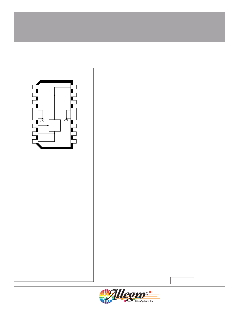
1
2
3
4
5
12
13
14
15
16
GROUND
Dwg. PS-018
6
7
10
11
8
9
GROUND
GROUND
GROUND
NC
NC
NC
OUT
IN
IN
ENABLE
NC
NC
NC
NC
OUT
VR
5 V
8181
LOW-DROPOUT,
5 V REGULATOR
115 Northeast Cutoff, Box 15036
Worcester, Massachusetts 01615-0036 (508) 853-5000
Maximum Allowable Output Current in Milliamperes with V
I
= 10 V, T
J
= 150
°
C*
dc (Duty Cycle)
T
A
100%
90%
80%
70%
60%
50%
40%
30%
20%
25
°
C
370
415
465
530
620
745
930
1000
1000
50
°
C
295
330
370
425
495
595
745
995
1000
70
°
C
235
265
295
340
395
475
595
795
1000
85
°
C
190
215
240
275
320
385
485
645
970
* I
O
= (T
J
- T
A
)/([V
I
- V
O
] R
θ
JA
• dc) = (150 - T
A
)/(5 • 67 • dc)
Output current rating can be increased (to 1 A maximum) by heat sinking or reducing the input voltage. With an infinite heat sink, R
-JA
= R
-JT
=
6
°
C/W. Conditions that produce excessive junction temperature will activate device thermal shutdown circuitry. These conditions can be tolerated
but should be avoided.
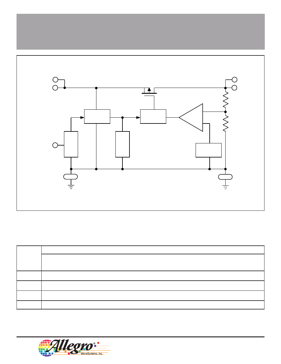
FUNCTIONAL BLOCK DIAGRAM
12-13
Dwg. FS-012
BIAS
DRIVE
ENABLE
THERMAL
PROTECT.
BANDGAP
REF.
ERROR
AMP
4-5
IN
ENABLE
OUT
IN
OUT
7
8
15
16
6
MAXIMUM ALLOWABLE OUTPUT CURRENT with device mounted on 2.24" x 2.24"
(56.9 mm x 56.9 mm) solder-coated copper-clad board in still air.
W
Copyright © 1992, 1995 Allegro MicroSystems, Inc.
8181
LOW-DROPOUT,
5 V REGULATOR
ELECTRICAL CHARACTERISTICS at T
A
+25
°
C (unless otherwise noted).
Limits
Characteristic
Symbol
Test Conditions
Min.
Typ.
Max.
Units
Output Voltage
V
O
T
A
= 25
°
C, 5.5 V
≤
V
I
≤
10 V,
4.90
5.00
5.10
V
0 mA
≤
I
O
≤
500 mA†
T
A
= 85
°
C, 5.5 V
≤
V
I
≤
10 V,
4.85
—
5.15
V
0 mA
≤
I
O
≤
500 mA*†
Output Volt. Temp. Coeff.
α
VO
I
O
= 0
—
±
100
—
µ
V/
°
C
Line Regulation
∆
V
O(
∆
VI)
5.5 V
≤
V
I
≤
10 V, Output open
—
10
30
mV
Load Regulation
∆
V
O(
∆
IO)
0 mA
≤
I
O
≤
500 mA†, V
I
= 6 V
—
40
100
mV
Dropout Voltage
V
I
min - V
O
I
O
= 500 mA†
—
—
300
mV
Quiescent Current
I
Q
V
I
= 10 V, I
O
= 500 mA†
—
87
120
µ
A
V
I
= 10 V, Output open
—
86
120
µ
A
I
Q(off)
V
I
= 10 V, Output open, V
E
= 0.4 V
—
—
20
µ
A
ENABLE Input Voltage
V
EH
Output ON, V
I
= 10 V
2.4
—
—
V
V
EL
Output OFF, V
I
= 10 V
—
—
0.4
V
ENABLE Input Current
I
E
V
E
= V
I
= 10 V
—
—
±
0.1
µ
A
Thermal Shutdown Temp.
T
J
—
165
—
°
C
Thermal Resistance
R
θ
JA
Mounted on 2.24" x 2.24" solder-coated
—
67
—
°
C/W
copper-clad board in still air
R
θ
JT
—
6.0
—
°
C/W
Typical values are given for circuit design information only.
* This parameter is tested to a lot sample plan only.
† Pulse test (<20 ms).
(GND terminal current)
8181
LOW-DROPOUT,
5 V REGULATOR
115 Northeast Cutoff, Box 15036
Worcester, Massachusetts 01615-0036 (508) 853-5000
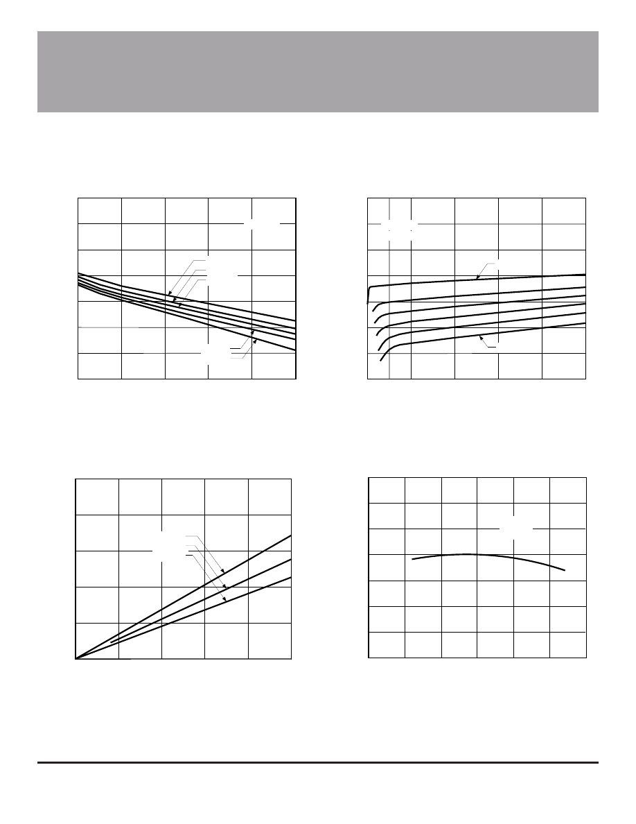
0
OUTPUT CURRENT, I
O
in mA
Dwg. GP-039-1
100
200
400
500
300
T = 25
°
C
A
5.04
5.00
5.02
4.98
OUTPUT VOLTAGE, V
O
in VOLTS
4.96
4.94
5.06
4.92
V = 7 V
I
V = 6 V
I
V = 8 V
I
V = 10 V
I
V = 5.5 V
I
5.0
Dwg. GP-040-1
6.0
7.0
9.0
10
8.0
T = 25
°
C
A
5.04
5.00
5.02
4.98
OUTPUT VOLTAGE, V
O
in VOLTS
4.96
4.94
5.06
4.92
I = 0 mA
O
I = 500 mA
O
INPUT VOLTAGE, V
I
in VOLTS
100 mA INTERVALS
CAUTION:
Maximum allowable duty cycle will be significantly less than 100% at high temperatures, at high input voltages, or at high output
currents. See Maximum Allowable Output Current table.
TYPICAL CHARACTERISTICS
5.0
Dwg. GP-040
6.0
7.0
9.0
10
8.0
T = -20
°
C
A
5.04
5.00
5.02
4.98
OUTPUT VOLTAGE, V
O
in VOLTS
4.96
4.94
5.06
4.92
I = 0 mA
O
INPUT VOLTAGE, V
I
in VOLTS
100 mA INTERVALS
I = 500 mA
O
0
OUTPUT CURRENT, I
O
in mA
Dwg. GP-039
100
200
400
500
300
V = 7 V
I
V = 6 V
I
V = 8 V
I
V = 10 V
I
T = -20
°
C
A
5.04
5.00
5.02
4.98
OUTPUT VOLTAGE, V
O
in VOLTS
4.96
4.94
5.06
4.92
V = 5.5 V
I
LOAD REGULATION
LINE REGULATION
8181
LOW-DROPOUT,
5 V REGULATOR
0
OUTPUT CURRENT, I
O
in mA
Dwg. GP-041
100
200
400
500
300
T = -20
°
C
T = 25
°
C
T = 85
°
C
A
A
A
0.3
0.4
0.2
DROPOUT VOLTAGE in VOLTS
0.1
0.5
0
DROPOUT VOLTAGE
OUTPUT VOLTAGE vs TEMP.
CAUTION:
Maximum allowable duty cycle will be significantly less than 100% at high temperatures, at high input voltages, or at high output
currents. See Maximum Allowable Output Current table.
TYPICAL CHARACTERISTICS (cont’d)
5.0
Dwg. GP-040-2
6.0
7.0
9.0
10
8.0
T = 85
°
C
A
5.04
5.00
5.02
4.98
OUTPUT VOLTAGE, V
O
in VOLTS
4.96
4.94
5.06
4.92
I = 0 mA
O
I = 500 mA
O
INPUT VOLTAGE, V
I
in VOLTS
100 mA INTERVALS
0
OUTPUT CURRENT, I
O
in mA
Dwg. GP-039-2
100
200
400
500
300
T = 85
°
C
A
5.04
5.00
5.02
4.98
OUTPUT VOLTAGE, V
O
in VOLTS
4.96
4.94
5.06
4.92
V = 7 V
I
V = 6 V
I
V = 8 V
I
V = 10 V
I
V = 5.5 V
I
LOAD REGULATION
LINE REGULATION
-50
AMBIENT TEMPERATURE, T
A
in
°
C
Dwg. GP-036
5.01
4.99
0
+50
5.00
+100
4.98
OUTPUT VOLTAGE, V
O
in VOLTS
V = 6 V
I = 0 mA
I
O
8181
LOW-DROPOUT,
5 V REGULATOR
115 Northeast Cutoff, Box 15036
Worcester, Massachusetts 01615-0036 (508) 853-5000
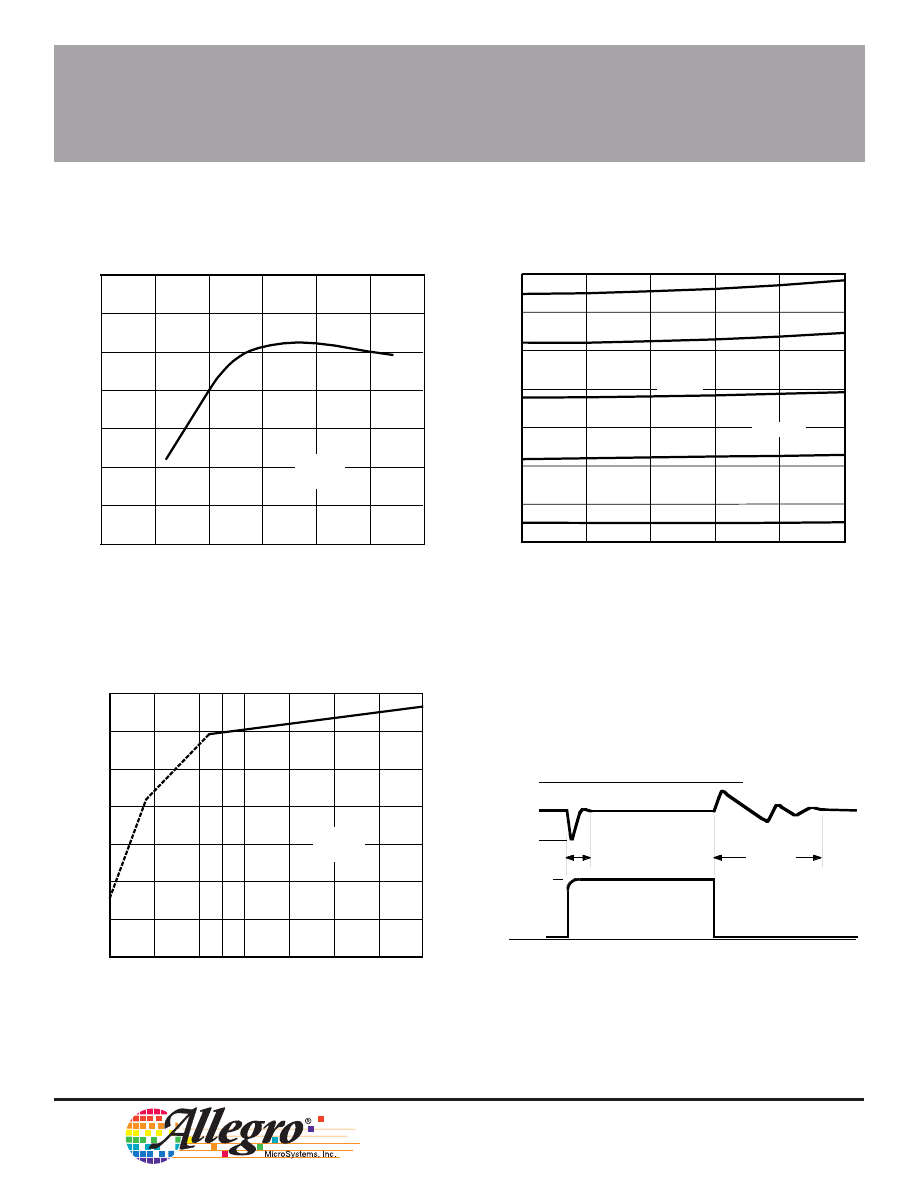
4.0
Dwg. GP-042
6.0
7.0
9.0
10
8.0
INPUT VOLTAGE, V
I
in VOLTS
20
90
70
60
50
80
QUIESCENT (GROUND TERMINAL) CURRENT in
µ
A
40
30
5.0
3.0
T = 25
°
C
A
I = 0 mA
O
TRANSIENT PERFORMANCE
Dwg. WP-018
VO
IO
500 mA
20 mA
5.5 V
5.0 V
4.5 V
<100
µ
s
<500
µ
s
V
I
= 5.5 V to 10 V, T
A
= -20
°
C to +85
°
C, C
O
= 4.7
µ
F
CAUTION:
Maximum allowable duty cycle will be significantly less than 100% at high temperatures, at high input voltages, or at high output
currents. See Maximum Allowable Output Current table.
TYPICAL CHARACTERISTICS (cont’d)
0
80
OUTPUT CURRENT, I
O
in mA
Dwg. GP-038
87
85
84
83
100
200
400
500
86
300
QUIESCENT (GROUND TERMINAL) CURRENT in
µ
A
82
81
V = 7 V
V = 6 V
V = 8 V
V = 9 V
V = 10 V
I
I
I
I
I
T = 25
°
C
A
-50
AMBIENT TEMPERATURE, T
A
in
°
C
Dwg. GP-037
80
0
+50
79
+100
78
V = 6 V
I = 0 mA
I
O
QUIESCENT (GROUND TERMINAL) CURRENT in
µ
A
81
QUIESCENT (GROUND TERMINAL) CURRENT
8181
LOW-DROPOUT,
5 V REGULATOR
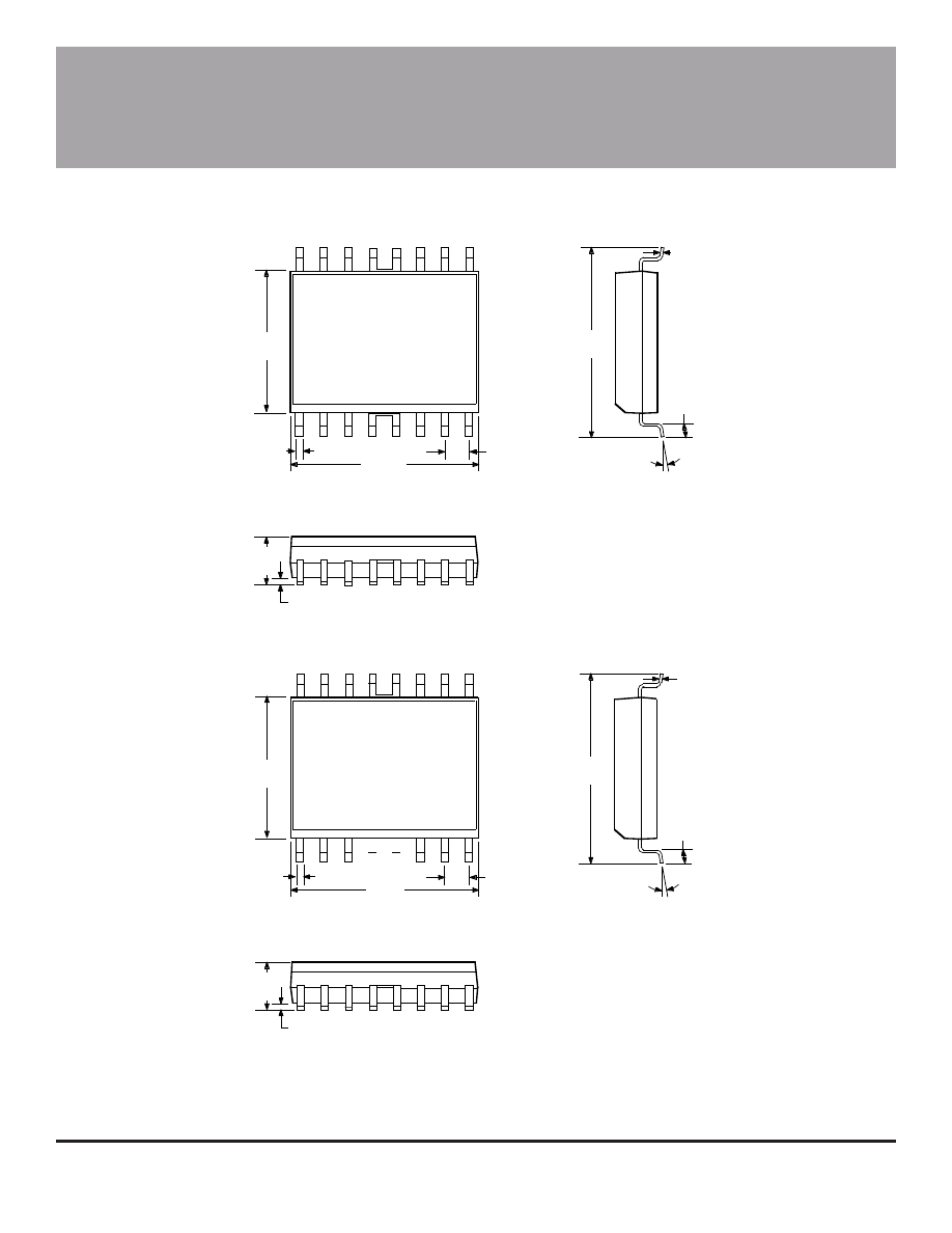
Dimensions in Inches
(Based on 1 mm = 0.3937”)
NOTES: 1. Webbed lead frames. Leads 4, 5, 12, and 13 are internally one piece.
2. Lead spring tolerance is non-cumulative.
3. Exact body and lead configuration at vendor’s option within limits shown.
Dimensions in Millimeters
0
°
TO
8
°
1
2
3
0.2992
0.2914
0.4133
0.3977
0.419
0.394
0.020
0.013
0.0926
0.1043
0.0040
MIN.
0.0125
0.0091
0.050
0.016
Dwg. MA-008-17A in
0.050
BSC
16
9
0
°
TO
8
°
9
1
16
2
3
7.60
7.40
10.50
10.10
10.65
10.00
0.51
0.33
2.65
2.35
0.10
MIN.
0.32
0.23
1.27
0.40
Dwg. MA-008-17A mm
1.27
BSC

8181
LOW-DROPOUT,
5 V REGULATOR
115 Northeast Cutoff, Box 15036
Worcester, Massachusetts 01615-0036 (508) 853-5000
Allegro MicroSystems, Inc. reserves the right to make, from time to time, such departures from
the detail specifications as may be required to permit improvements in the design of its products.
Components made under military approvals will be in accordance with the approval requirements.
The information included herein is believed to be accurate and reliable. However, Allegro
MicroSystems, Inc. assumes no responsibility for its use; nor for any infringements of patents or other
rights of third parties which may result from its use.
Wyszukiwarka
Podobne podstrony:
więcej podobnych podstron