TDA7376B
2 x 35W POWER AMPLIFIER FOR CAR RADIO
HIGH OUTPUT POWER CAPABILITY:
2 x 40W max./4
Ω
2 x 35W/4
Ω
EIAJ
2 x 25W4
Ω
@ 14.4V, 1KHz, 10%
2 x 37W2
Ω
@ 14.4V, 1KHz, 10%
2
Ω
DRIVING
DIFFERENTIAL INPUTS
MINIMUM EXTERNAL COMPONENT COUNT
INTERNALLY FIXED GAIN (26dB)
MUTE FUNCTION (CMOS COMPATIBLE)
AUTOMUTE AT MINIMUM SUPPLY VOLT-
AGE DETECTION
STAND-BY FUNCTION
NO AUDIBLE POP DURING MUTE AND ST-
BY OPERATIONS
CLIPPING DETECTOR WITH PROGRAMMA-
BLE DISTORTION THRESHOLD
PROTECTIONS:
SHORT CIRCUIT (OUT TO GROUND, OUT
TO
SUPPLY
VOLTAGE,
ACROSS
THE
LOAD)
OVERRATING CHIP TEMPERATURE WITH
SOFT THERMAL LIMITER
LOAD DUMP VOLTAGE
FORTUITOUS OPEN GROUND
LOUDSPEAKER DC CURRENT
ESD
DESCRIPTION
The TDA7376B is a new technology dual bridge
Audio Amplifier in Multiwatt 15 package designed
for car radio applications. Thanks to the fully com-
plementary PNP/NPN output stage configuration
the TDA7376B delivers a rail-to-rail voltage swing
with no need of bootstrap capacitors. Differential
input pairs, that will accept either single ended or
differential input signals, guarantee high noise im-
munity making the device suitable for both car ra-
dio and car boosters applications.
The audio mute control, that attenuates the out-
put signal of the audio amplifiers, suppresses pop
on - off transients and cuts any noises coming
from previous stages. The St-By control, that de-
biases the amplifiers, reduces the cost of the
power switch. The on-board programmable distor-
tion detector allows compression facility when-
ever the ampifier is overdriven, so limiting the dis-
tortion at any levels inside the presettable range.
This is advanced information on a new product now in development or undergoing evaluation. Details are subject to change without notice.
May 2000
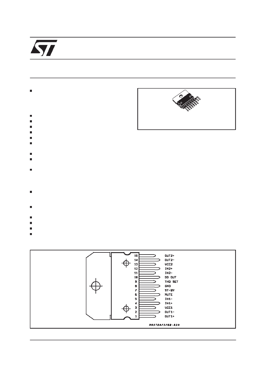
PIN CONNECTION (Continued)
MULTIWATT15
ORDERING NUMBER: TDA7376B
1/9
ABSOLUTE MAXIMUM RATINGS
Symbol
Parameter
Value
Unit
V
OP
Operating Supply Voltage
18
V
V
S
DC Supply Voltage
28
V
V
peak
Peak Supply Voltage (t = 50ms)
50
V
I
O
Output Peak Current (non rep. t = 100
µ
s)
Output Peak Current (rep. f > 10Hz)
8
6
A
A
P
tot
Power Dissipation at T
case
= 85
°
C
36
W
T
stg,
T
j
Storage and Junction Temperature
–40 to 150
°
C
THERMAL DATA
Symbol
Parameter
Value
Unit
R
th j-case
Thermal Resistance Junction-case
max.
1.8
°
C/W
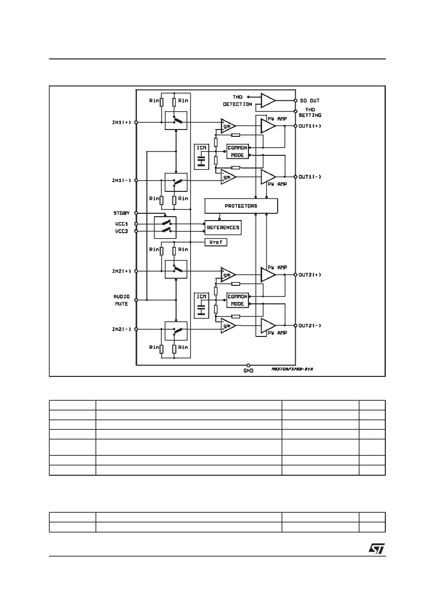
BLOCK DIAGRAM
TDA7376B
2/9
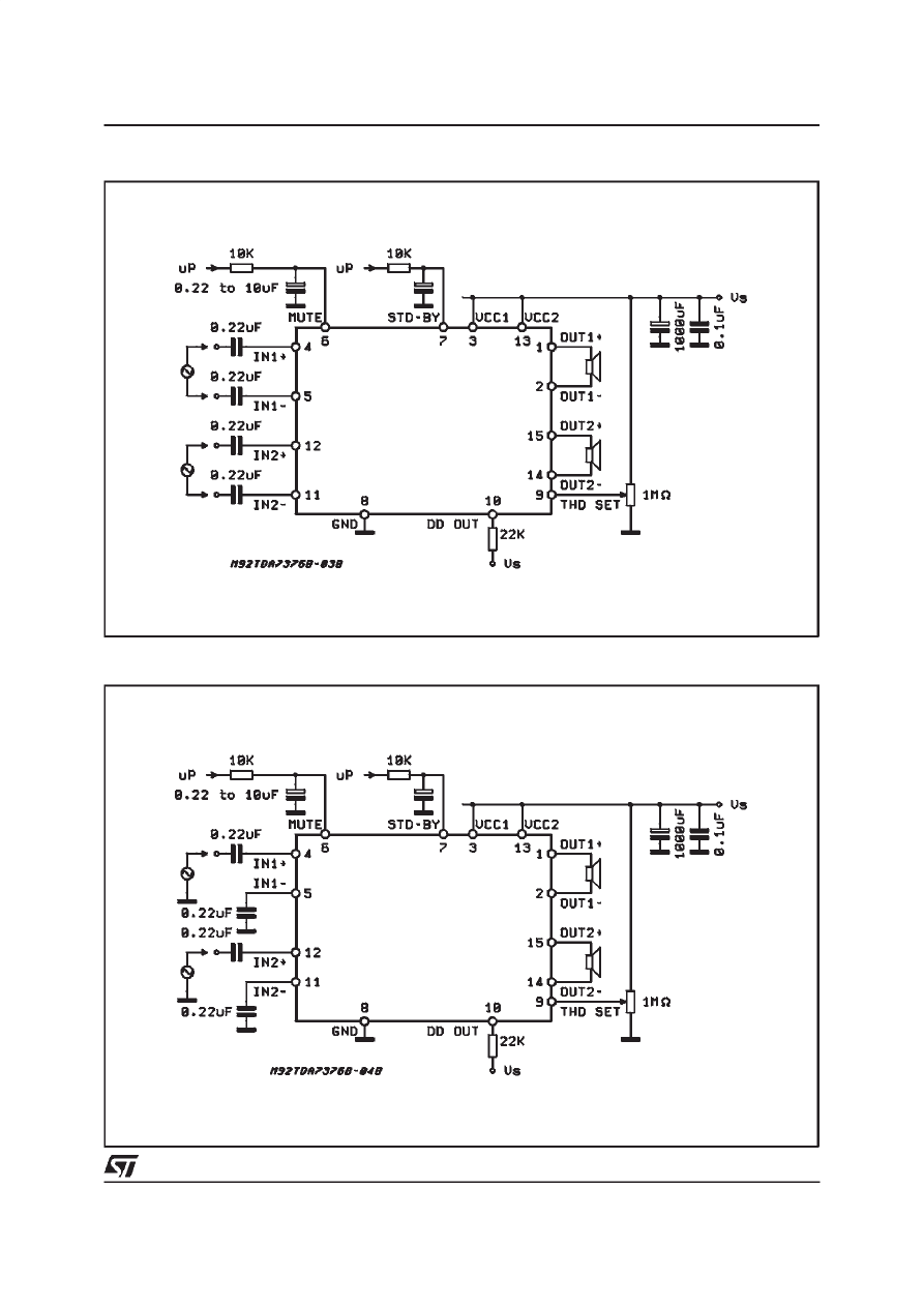
Figure 1: Differential Inputs Test and Application Circuit
Figure 2: Single Ended Inputs Test and Application Circuit
1
µ
F
1
µ
F
TDA7376B
3/9
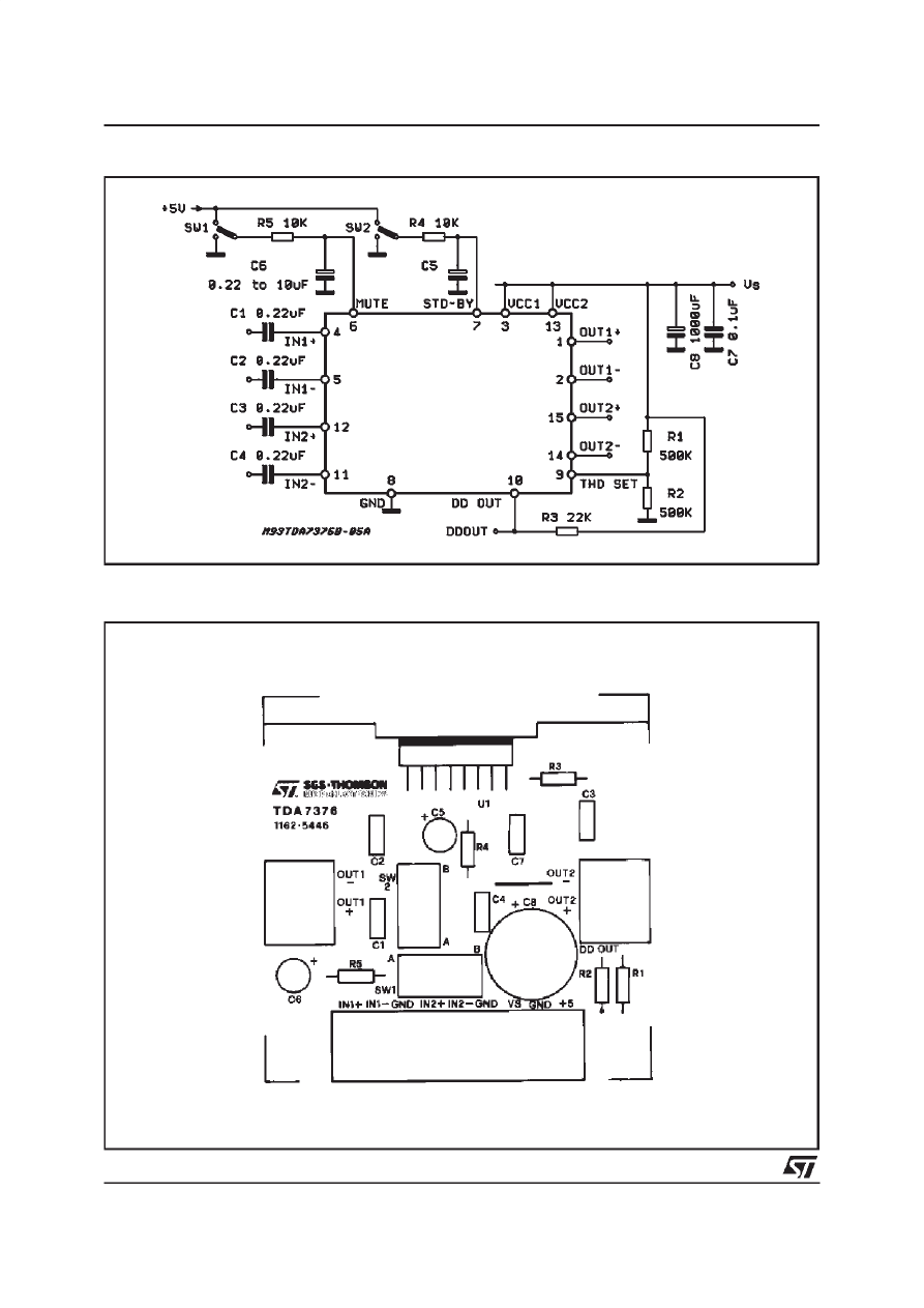
Figure 3: Application Board Reference Circuit
Figure 4: P.C. Board and Components Layout of the Circuit of Fig. 3 (1:1 scale)
1
µ
F
TDA7376B
4/9
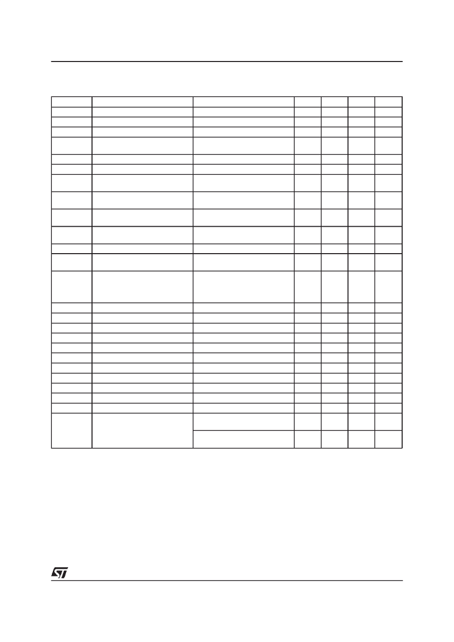
ELECTRICAL CHARACTERISTICS (Refer to the test fig. 1 and 2 circuit, T
amb
= 25
°
C; V
S
= 14.4V;
f = 1KHz; R
L
= 4
Ω
; unless otherwise specified.)
Symbol
Parameter
Test Condition
Min.
Typ.
Max.
Unit
V
S
Supply Voltage
8
18
V
I
d
Total Quiescent Drain Current
R
L
=
∞
200
mA
V
OS
Output Offset Voltage
120
mV
P
O
Output Power
THD = 10%
THD = 10%, R
L
2
Ω
23
33
25
37
W
W
P
O max
Max. Output Power (*)
VS = 14.4V
36
40
W
P
O EIAJ
EIAJ Output Power (*)
V
S
= 13.7V
32
35
W
THD
Distortion
P
O
= 0.5 to 10W
P
O
= 0.5 to 15W
0.03
0.08
0.3
0.5
%
%
C
T
Cross Talk
f = 1KHz; Rg = 0
f = 10KHz; Rg = 0
80
70
dB
dB
R
IN
Input Resistance
differential input
single ended input
45
40
K
Ω
K
Ω
G
V
Voltage Gain
differential input
single ended input
25
25
26
26
27
27
dB
dB
∆
G
V
Channel Gain Balance
1
dB
E
N
Input Noise Voltage
Rg = 600
Ω
; ”A Weighted”
Rg = 600
Ω
; 22Hz to 22KHz
3
4
6
µ
V
µ
V
SVR
Supply Voltage Rejection
f = 100Hz; Vr = 1Vrms;
Rg = 0
f = 10KHz; Vr = 1Vrms;
Rg = 0
45
55
dB
dB
BW
Power Bandwidth
(–3dB)
75
KHz
CMRR
Common Mode Rejection Ratio
V
CM
= 1Vrms input referred
60
dB
A
SB
Stand-by Attenuation
V
SB
= 1.5V; P
Oref
= 1W
80
90
dB
V
sb IN
Stand-by in Threshold
1.5
V
V
sb OUT
Stand-by out Threshold
3.5
V
I
sb
Stand-by Current Consumption
100
µ
A
A
M
Mute Attenuation
V
M
= 1.5V; P
Oref
= 1W
85
dB
V
M IN
Mute in Threshold
1.5
V
V
M OUT
Mute out Threshold
3.5
V
I
6
Mute pin Current
V6 = 0 to V
S
, ; V
S max.
= 18V
100
µ
A
D
DL
Distortion Detection Level (**)
3.5
%
D
DOUT
Distortion Detector Output DC
Current
Output low, sinked current
(V
pin10
= 1.5V)
1
mA
Output high, leakage current
(V
pin10
= V
S
, @ V
Smax
= 18V)
10
µ
A
(*) Saturated square wave output
(**) see figure 5 for THD setting.
The TDA7376B is equipped with a programmable
clipping distortion detector circuitry that allows to
signal out the output stage saturation by providing
a current sinking into an open collector output
(DDout) when the total harmonic distortion of the
output signal reaches the preset level. The de-
sired threshold is fixed through an external divider
that produces a proper voltage level across the
THD set pin. Fig. 5 shows the THD detection
threshold versus the THD set voltage. Since it is
essential that the THD set voltage be proportional
to the supply voltage, fig. 5 shows its value as a
fraction of V
CC
. The actual voltage can be com-
puted by multiplying the fraction corresponding to
the desired THD threshold by the application’s
supply voltage.
TDA7376B
5/9
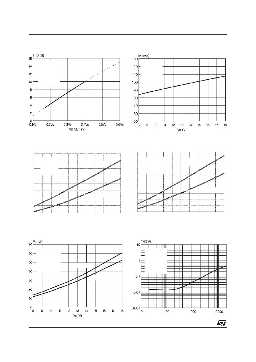
Figure 5: Clip Detector Threshold vs. THD set.
Voltage.
8
9
10
11
12
13
14
15
16
17
18
Vs (V)
5
10
15
20
25
30
35
40
45
50
55
Po (W)
f= 1 KHz
THD= 10 %
RL= 2
Ω
RL= 4
Ω
Figure 8: Ouput Power vs. Supply Voltage
Figure 6: Quiescent Current vs. Supply Voltage
8
9
10
11
12
13
14
15
16
17
18
Vs (V)
5
10
15
20
25
30
35
40
45
Po (W)
f= 1 KHz
THD= 1 %
RL= 2
Ω
RL= 4
Ω
Figure 7: Ouput Power vs. Supply Voltage
Figure 9: EIAJ Power vs. Supply Voltage
R
L
= 4
Ω
R
L
= 4
Ω
R
L
= 3.2
Ω
f = 1KHz
V
i
= 2.5Vrms
Figure 10: THD vs. Frequency
V
S
= 14.4V
R
L
= 4
Ω
P
O
= 12W
f (Hz)
V
S
= 14.4V
R
L
= 4
Ω
f = 1KHz
TDA7376B
6/9

Figure 15: CMRR vs. Frequency
0.1
1
10
Po(W)
0.01
0.1
1
10
THD(%)
Vs= 14.4V
RL= 4
Ω
f=10KHz
f =1 KHz
Figure 11: THD vs. Output Power (R
L
= 4
Ω
)
Figure 14: SVR vs. Frequency
Figure 16: Crosstalk vs. Frequency
Figure 13: Dissipated Power & Efficiency vs. Out-
put Power
V
S
= 14.4V
R
L
= 4
Ω
f = 1KHz
f (Hz)
V
S
= 14.4V
R
L
= 4
Ω
V
r
= 1Vrms
V
S
= 14.4V
R
L
= 4
Ω
V
i
= 1Vrms
R
i
= 0
R
i
= 600
Ω
V
S
= 14.4V
R
L
= 4
Ω
P
O
= 1W
R
L
= 0
f (Hz)
f (Hz)
0.1
1
10
Po(W)
0.01
0.1
1
10
THD(%)
Vs=14.4V
R L = 2
Ω
f = 10 KHz
f= 1KHz
Figure 12: THD vs. Output Power (R
L
= 24
Ω
)
TDA7376B
7/9
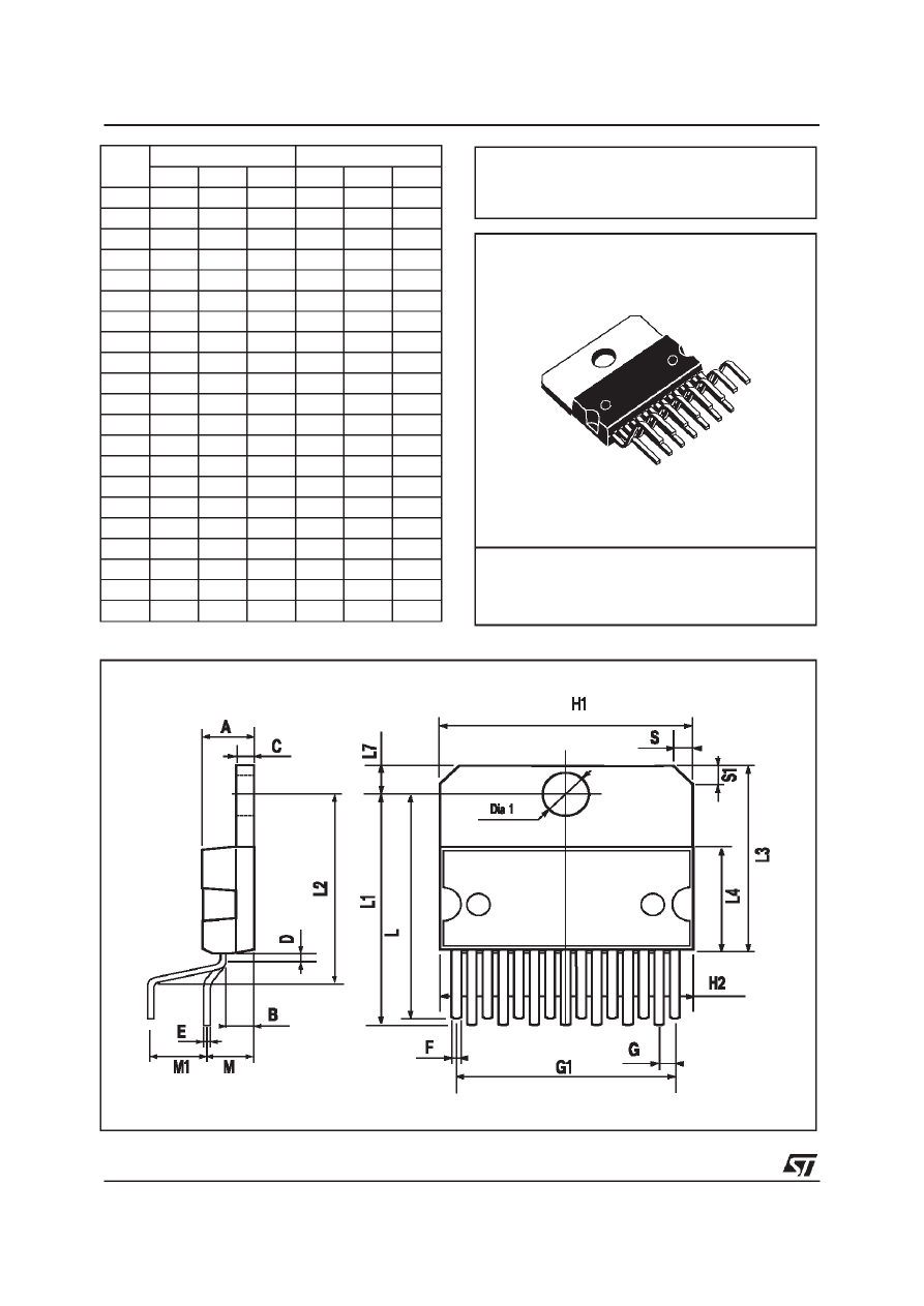
Multiwatt15 V
DIM.
mm
inch
MIN.
TYP.
MAX.
MIN.
TYP.
MAX.
A
5
0.197
B
2.65
0.104
C
1.6
0.063
D
1
0.039
E
0.49
0.55
0.019
0.022
F
0.66
0.75
0.026
0.030
G
1.02
1.27
1.52
0.040
0.050
0.060
G1
17.53
17.78
18.03
0.690
0.700
0.710
H1
19.6
0.772
H2
20.2
0.795
L
21.9
22.2
22.5
0.862
0.874
0.886
L1
21.7
22.1
22.5
0.854
0.870
0.886
L2
17.65
18.1
0.695
0.713
L3
17.25
17.5
17.75
0.679
0.689
0.699
L4
10.3
10.7
10.9
0.406
0.421
0.429
L7
2.65
2.9
0.104
0.114
M
4.25
4.55
4.85
0.167
0.179
0.191
M1
4.63
5.08
5.53
0.182
0.200
0.218
S
1.9
2.6
0.075
0.102
S1
1.9
2.6
0.075
0.102
Dia1
3.65
3.85
0.144
0.152
OUTLINE AND
MECHANICAL DATA
TDA7376B
8/9

Information furnished is believed to be accurate and reliable. However, STMicroelectronics assumes no responsibility for the consequences
of use of such information nor for any infringement of patents or other rights of third parti es which may result from its use. No license is
granted by implication or otherwise under any patent or patent rights of STMicroelectronics. Specification mentioned in this publication are
subject to change without notice. This publication supersedes and replaces all information previously supplied. STMicroelectronics products
are not authorized for use as critical components in life support devices or systems without express written approval of STMicroelectronics.
The ST logo is a registered trademark of STMicroelectronics
2001 STMicroelectronics – Printed in Italy – All Rights Reserved
STMicroelectronics GROUP OF COMPANIES
Australia - Brazil - China - Finland - France - Germany - Hong Kong - India - Italy - Japan - Malaysia - Malta - Morocco -
Singapore - Spain - Sweden - Switzerland - United Kingdom - U.S.A.
http://www.st.com
TDA7376B
9/9
Wyszukiwarka
Podobne podstrony:
więcej podobnych podstron