
Chapter 8
Current-Feedback Op Amp Analysis
Literature Number SLOA080
Excerpted from
Op Amps for Everyone
Literature Number: SLOD006A

8-1
Current-Feedback Op Amp Analysis
Ron Mancini
8.1
Introduction
Current-feedback amplifiers (CFA) do not have the traditional differential amplifier input
structure, thus they sacrifice the parameter matching inherent to that structure. The CFA
circuit configuration prevents them from obtaining the precision of voltage-feedback am-
plifiers (VFA), but the circuit configuration that sacrifices precision results in increased
bandwidth and slew rate. The higher bandwidth is relatively independent of closed-loop
gain, so the constant gain-bandwidth restriction applied to VFAs is removed for CFAs. The
slew rate of CFAs is much improved from their counterpart VFAs because their structure
enables the output stage to supply slewing current until the output reaches its final value.
In general, VFAs are used for precision and general purpose applications, while CFAs are
restricted to high frequency applications above 100 MHz.
Although CFAs do not have the precision of their VFA counterparts, they are precise
enough to be dc-coupled in video applications where dynamic range requirements are not
severe. CFAs, unlike previous generation high-frequency amplifiers, have eliminated the
ac coupling requirement; they are usually dc-coupled while they operate in the GHz
range. CFAs have much faster slew rates than VFAs, so they have faster rise/fall times
and less intermodulation distortion.
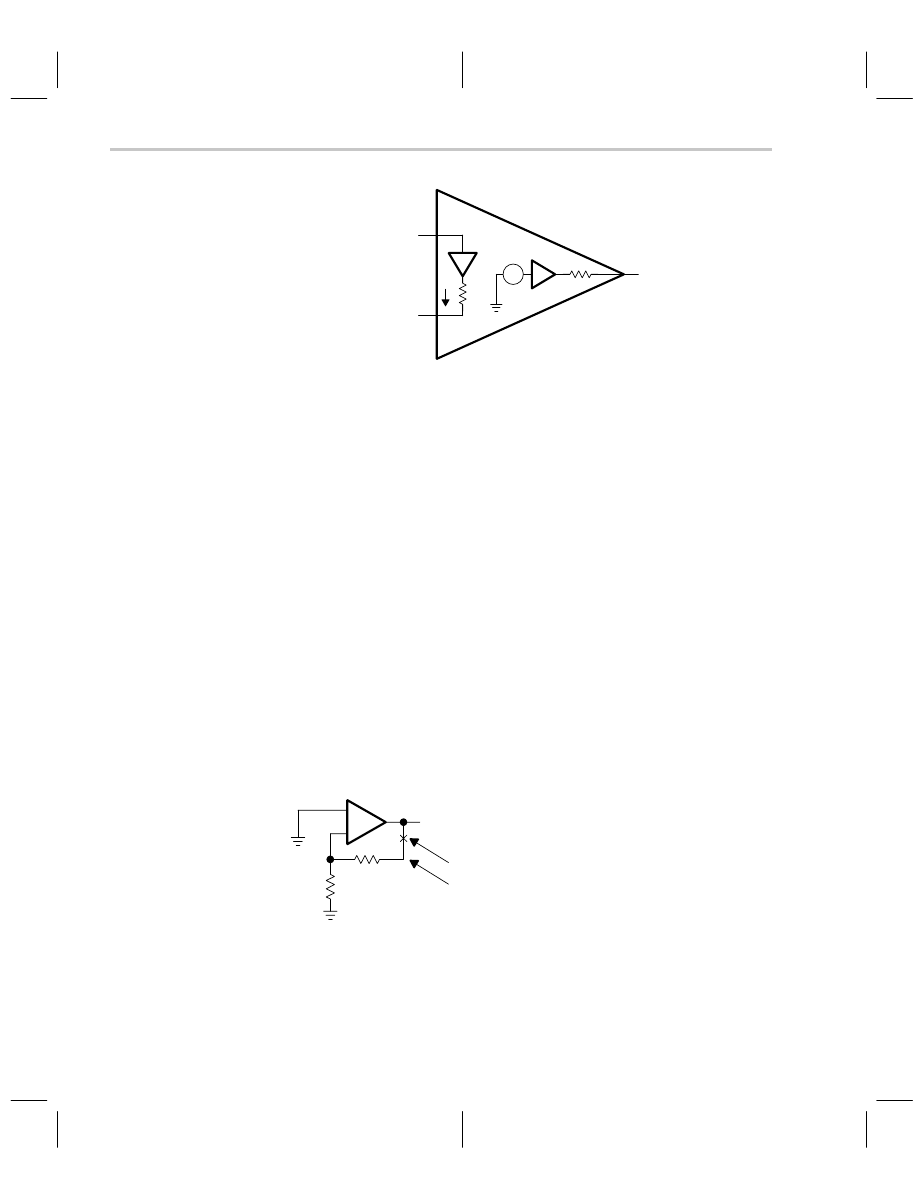
8.2
CFA Model
The CFA model is shown in Figure 8–1. The noninverting input of a CFA connects to the
input of the input buffer, so it has very high impedance similar to that of a bipolar transistor
noninverting VFA input. The inverting input connects to the input buffer’s output, so the
inverting input impedance is equivalent to a buffer’s output impedance, which is very low.
Z
B
models the input buffer’s output impedance, and it is usually less than 50
Ω
. The input
buffer gain, G
B
, is as close to one as IC design methods can achieve, and it is small
enough to neglect in the calculations.
Chapter 8
Development of the Stability Equation
8-2
ZOUT
GOUT
Z(I)
ZB
GB
I
VOUT
+
–
NONINVERTING INPUT
INVERTING INPUT
Figure 8–1. Current-Feedback Amplifier Model
The output buffer provides low output impedance for the amplifier. Again, the output buffer
gain, G
OUT
, is very close to one, so it is neglected in the analysis. The output impedance
of the output buffer is ignored during the calculations. This parameter may influence the
circuit performance when driving very low impedance or capacitive loads, but this is usual-
ly not the case. The input buffer’s output impedance can’t be ignored because affects sta-
bility at high frequencies.
The current-controlled current source, Z, is a transimpedance. The transimpedance in a
CFA serves the same function as gain in a VFA; it is the parameter that makes the perfor-
mance of the op amp dependent only on the passive parameter values. Usually the trans-
impedance is very high, in the M
Ω
range, so the CFA gains accuracy by closing a feed-
back loop in the same manner that the VFA does.
8.3
Development of the Stability Equation
The stability equation is developed with the aid of Figure 8–2. Remember, stability is inde-
pendent of the input, and stability depends solely on the loop gain, A
β
. Breaking the loop
at point X, inserting a test signal, V
TI
, and calculating the return signal V
TO
develops the
stability equation.
_
+
CFA
ZF
ZG
VOUT Becomes VTO; The Test Signal Output
Break Loop Here
Apply Test Signal (VTI) Here
Figure 8–2. Stability Analysis Circuit
The circuit used for stability calculations is shown in Figure 8–3 where the model of Figure
8–1 is substituted for the CFA symbol. The input and output buffer gain, and output buffer
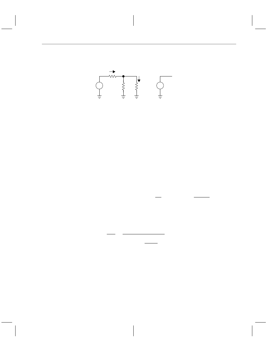
The Noninverting CFA
8-3
Current-Feedback Op Amp Analysis
output impedance have been deleted from the circuit to simplify calculations. This approx-
imation is valid for almost all applications.
ZF
I2
+
VTI
ZG
ZB
I1Z
I1
VOUT = VTO
Figure 8–3. Stability Analysis Circuit
The transfer equation is given in Equation 8–1, and the Kirchoff”s law is used to write
Equations 8–2 and 8–3.
(8–1)
V
TO
+
I
1
Z
(8–2)
V
TI
+
I
2
ǒ
Z
F
)
Z
G
ø
Z
B
Ǔ
(8–3)
I
2
ǒ
Z
G
ø
Z
B
Ǔ
+
I
1
Z
B
Equations 8–2 and 8–3 are combined to yield Equation 8–4.
(8–4)
V
TI
+
I
1
ǒ
Z
F
)
Z
G
ø
Z
B
Ǔ
ǒ
1
)
Z
B
Z
G
Ǔ
+
I
1
Z
F
ǒ
1
)
Z
B
Z
F
ø
Z
G
Ǔ
Dividing Equation 8–1 by Equation 8–4 yields Equation 8–5, and this is the open loop
transfer equation. This equation is commonly known as the loop gain.
(8–5)
A
b +
V
TO
V
TI
+
Z
ǒ
Z
F
ǒ
1
)
Z
B
Z
F
ø
Z
G
Ǔ
Ǔ
8.4
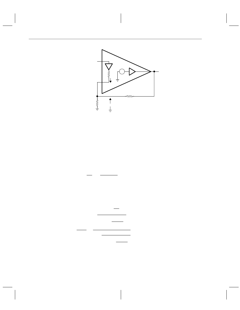
The Noninverting CFA
The closed-loop gain equation for the noninverting CFA is developed with the aid of Figure
8–4, where external gain setting resistors have been added to the circuit. The buffers are
shown in Figure 8–4, but because their gains equal one and they are included within the
feedback loop, the buffer gain does not enter into the calculations.
The Noninverting CFA
8-4
G = 1
IZ
ZB
G = 1
I
VOUT
+
–
VIN
+
VA
ZG
ZF
Figure 8–4. Noninverting CFA
Equation 8–6 is the transfer equation, Equation 8–7 is the current equation at the inverting
node, and Equation 8–8 is the input loop equation. These equations are combined to yield
the closed-loop gain equation, Equation 8–9.
(8–6)
V
OUT
+
IZ
(8–7)
I
+
ǒ
V
A
Z
G
Ǔ
–
ǒ
V
OUT
–V
A
Z
F
Ǔ
(8–8)
V
A
+
V
IN
–IZ
B
(8–9)
V
OUT
V
IN
+
Z
ǒ
1
)
Z
F
Z
G
Ǔ
Z
F
ǒ
1
)
Z
B
Z
F
ø
Z
G
Ǔ
1
)
Z
Z
F
ǒ
1
)
Z
B
Z
F
ø
Z
G
Ǔ
When the input buffer output impedance, Z
B
, approaches zero, Equation 8–9 reduces to
Equation 8–10.
The Inverting CFA
8-5
Current-Feedback Op Amp Analysis
(8–10)
V
OUT
V
IN
+
Z
ǒ
1
)
Z
F
Z
G
Ǔ
Z
F
1
)
Z
Z
F
+
1
)
Z
F
Z
G
1
)
Z
F
Z
When the transimpedance, Z, is very high, the term Z
F
/Z in Equation 8–10 approaches
zero, and Equation 8–10 reduces to Equation 8–11; the ideal closed-loop gain equation
for the CFA. The ideal closed-loop gain equations for the CFA and VFA are identical, and
the degree to which they depart from ideal is dependent on the validity of the assumptions.
The VFA has one assumption that the direct gain is very high, while the CFA has two as-
sumptions, that the transimpedance is very high and that the input buffer output imped-
ance is very low. As would be expected, two assumptions are much harder to meet than
one, thus the CFA departs from the ideal more than the VFA does.
(8–11)
V
OUT
V
IN
+
1
)
Z
F
Z
G
8.5
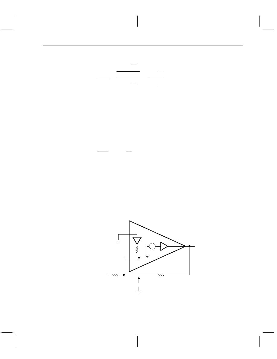
The Inverting CFA
The inverting CFA configuration is seldom used because the inverting input impedance
is very low (Z
B
||Z
F
+Z
G
). When Z
G
is made dominant by selecting it as a high resistance
value it overrides the effect of Z
B
. Z
F
must also be selected as a high value to achieve at
least unity gain, and high values for Z
F
result in poor bandwidth performance, as we will
see in the next section. If Z
G
is selected as a low value the frequency sensitive Z
B
causes
the gain to increase as frequency increases. These limitations restrict inverting applica-
tions of the inverting CFA.
G = 1
IZ
ZB
G = 1
I
VOUT
+
–
VIN
+
VA
ZG
ZF
Figure 8–5. Inverting CFA

The Inverting CFA
8-6
The current equation for the input node is written as Equation 8–12. Equation 8–13 de-
fines the dummy variable, V
A
, and Equation 8–14 is the transfer equation for the CFA.
These equations are combined and simplified leading to Equation 8–15, which is the
closed-loop gain equation for the inverting CFA.
(8–12)
I
)
V
IN
–V
A
Z
G
+
V
A
–V
OUT
Z
F
(8–13)
IZ
B
+
–V
A
(8–14)
IZ
+
V
OUT
(8–15)
V
OUT
V
IN
+ *
Z
Z
G
ǒ
1
)
Z
B
Z
F
ø
Z
G
Ǔ
1
)
Z
Z
F
ǒ
1
)
Z
B
Z
F
ø
Z
G
Ǔ
When Z
B
approaches zero, Equation 8–15 reduces to Equation 8–16.
(8–16)
V
OUT
V
IN
+
–
1
Z
G
1
Z
)
1
Z
F
When Z is very large, Equation 8–16 becomes Equation 8–17, which is the ideal closed-
loop gain equation for the inverting CFA.
(8–17)
V
OUT
V
IN
+
–
Z
F
Z
G
The ideal closed-loop gain equation for the inverting VFA and CFA op amps are identical.
Both configurations have lower input impedance than the noninverting configuration has,
but the VFA has one assumption while the CFA has two assumptions. Again, as was the
case with the noninverting counterparts, the CFA is less ideal than the VFA because of
the two assumptions. The zero Z
B
assumption always breaks down in bipolar junction
transistors as is shown later. The CFA is almost never used in the differential amplifier con-
figuration because of the CFA’s gross input impedance mismatch.
Stability Analysis
8-7
Current-Feedback Op Amp Analysis
8.6
Stability Analysis
The stability equation is repeated as Equation 8–18.
(8–18)
A
b +
V
TO
V
TI
+
Z
ǒ
Z
F
ǒ
1
)
Z
B
Z
F
ø
Z
G
Ǔ
Ǔ
Comparing Equations 8–9 and 8–15 to Equation 8–18 reveals that the inverting and non-
inverting CFA op amps have identical stability equations. This is the expected result be-
cause stability of any feedback circuit is a function of the loop gain, and the input signals
have no affect on stability. The two op amp parameters affecting stability are the trans-
impedance, Z, and the input buffer’s output impedance, Z
B
. The external components af-
fecting stability are Z
G
and Z
F
. The designer controls the external impedance, although
stray capacitance that is a part of the external impedance sometimes seems to be uncon-
trollable. Stray capacitance is the primary cause of ringing and overshoot in CFAs. Z and
Z
B
are CFA op amp parameters that can’t be controlled by the circuit designer, so he has
to live with them.
Prior to determining stability with a Bode plot, we take the log of Equation 8–18, and plot
the logs (Equations 8–19 and 8–20) in Figure 8–6.
(8–19)
20 LOG |A
b
|
+
20 LOG |Z|
*
20 LOG
Ť
Z
F
ǒ
1
)
Z
B
Z
F
ø
Z
B
Ǔ
Ť
(8–20)
f +
TANGENT
*
1
(A
b
)
This enables the designer to add and subtract components of the stability equation graph-
ically.
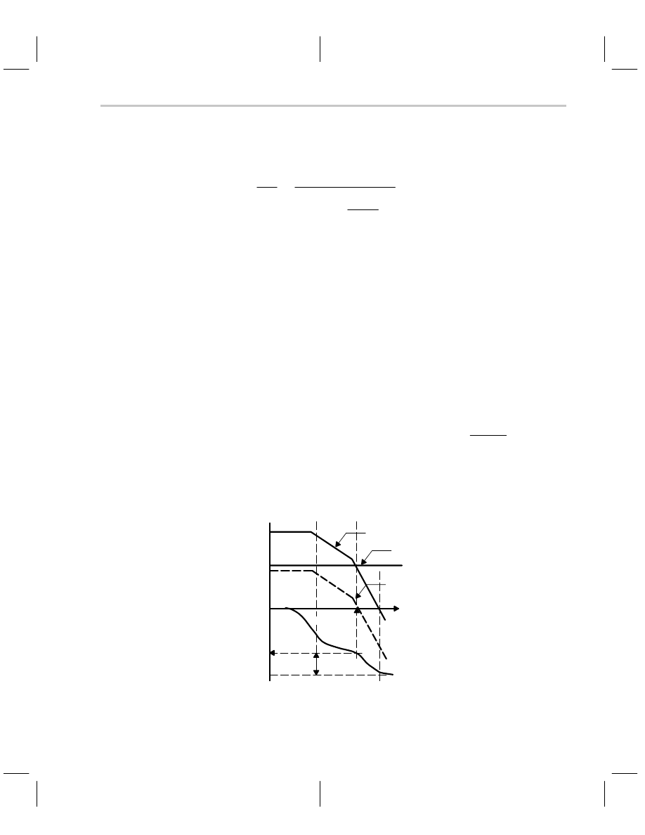
AMPLITUDE (dB )
Ω
120
61.1
58.9
0
–60
–120
–180
20LOGIZI
20LOGIZF(1 + ZB/ZFIIZG)I
Composite Curve
LOG(f)
ϕ
M = 60
°
1/
τ
1
1/
τ
2
PHASE
(DEGREES)
Figure 8–6. Bode Plot of Stability Equation

Stability Analysis
8-8
The plot in Figure 8–6 assumes typical values for the parameters:
(8–21)
Z
+
1M
W
ǒ
1
) t
1
S
Ǔǒ
1
) t
2
S
Ǔ
(8–22)
Z
B
+
70
W
(8–23)
Z
G
+
Z
F
+
1k
W
The transimpedance has two poles and the plot shows that the op amp will be unstable
without the addition of external components because 20 LOG|Z| crosses the 0-dB axis
after the phase shift is 180
°
. Z
F
,
Z
B
, and Z
G
reduce the loop gain 61.1 dB, so the circuit
is stable because it has 60
°
-phase margin. Z
F
is the component that stabilizes the circuit.
The parallel combination of Z
F
and Z
G
contribute little to the phase margin because Z
B
is very small, so Z
B
and Z
G
have little effect on stability.
The manufacturer determines the optimum value of R
F
during the characterization of the
IC. Referring to Figure 8–6, it is seen that when R
F
exceeds the optimum value recom-
mended by the IC manufacturer, stability increases. The increased stability has a price
called decreased bandwidth. Conversely, when R
F
is less than the optimum value recom-
mended by the IC manufacturer, stability decreases, and the circuit response to step in-
puts is overshoot or possibly ringing. Sometimes the overshoot associated with less than
optimum R
F
is tolerated because the bandwidth increases as R
F
decreases. The peaked
response associated with less than optimum values of R
F
can be used to compensate for
cable droop caused by cable capacitance.
When Z
B
= 0
Ω
and Z
F
= R
F
the loop gain equation is; A
β
= Z/R
F
. Under these conditions
Z and R
F
determine stability, and a value of R
F
can always be found to stabilize the circuit.
The transimpedance and feedback resistor have a major impact on stability, and the input
buffer’s output impedance has a minor effect on stability. Since Z
B
increases with an in-
crease in frequency, it tends to increase stability at higher frequencies. Equation 8–18 is
rewritten as Equation 8–24, but it has been manipulated so that the ideal closed-loop gain
is readily apparent.
(8–24)
A
b +
Z
Z
F
)
Z
B
ǒ
1
)
R
F
R
G
Ǔ
The closed-loop ideal gain equation (inverting and noninverting) shows up in the denomi-
nator of Equation 8–24, so the closed-loop gain influences the stability of the op amp.
When Z
B
approaches zero, the closed-loop gain term also approaches zero, and the op
amp becomes independent of the ideal closed-loop gain. Under these conditions R
F
de-
termines stability, and the bandwidth is independent of the closed-loop gain. Many people
claim that the CFA bandwidth is independent of the gain, and that claim’s validity is depen-
dent on the ratios Z
B
/Z
F
being very low.

Selection of the Feedback Resistor
8-9
Current-Feedback Op Amp Analysis
Z
B
is important enough to warrant further investigation, so the equation for Z
B
is given be-
low.
(8–25)
Z
B
^
h
ib
)
R
B
b
0
)
1
ȧȧ
ȡ
Ȣ
1
)
s
b
0
w
T
1
)
S
b
0
ǒb
0
)
1
Ǔw
T
ȧȧ
ȣ
Ȥ
At low frequencies h
ib
= 50
Ω
and R
B
/(
β
0
+1) = 25
Ω
, so Z
B
= 75
Ω
. Z
B
varies in accordance
with Equation 8–25 at high frequencies. Also, the transistor parameters in Equation 8–25
vary with transistor type; they are different for NPN and PNP transistors. Because Z
B
is
dependent on the output transistors being used, and this is a function of the quadrant the
output signal is in, Z
B
has an extremely wide variation. Z
B
is a small factor in the equation,
but it adds a lot of variability to the current-feedback op amp.
8.7
Selection of the Feedback Resistor
The feedback resistor determines stability, and it affects closed-loop bandwidth, so it must
be selected very carefully. Most CFA IC manufacturers employ applications and product
engineers who spend a great deal of time and effort selecting R
F
. They measure each non-
inverting gain with several different feedback resistors to gather data. Then they pick a
compromise value of R
F
that yields stable operation with acceptable peaking, and that
value of R
F
is recommended on the data sheet for that specific gain. This procedure is
repeated for several different gains in anticipation of the various gains their customer ap-
plications require (often G = 1, 2, or 5). When the value of R
F
or the gain is changed from
the values recommended on the data sheet, bandwidth and/or stability is affected.
When the circuit designer must select a different R
F
value from that recommended on the
data sheet he gets into stability or low bandwidth problems. Lowering R
F
decreases stabil-
ity, and increasing R
F
decreases bandwidth. What happens when the designer needs to
operate at a gain not specified on the data sheet? The designer must select a new value
of R
F
for the new gain, but there is no guarantee that new value of R
F
is an optimum value.
One solution to the R
F
selection problem is to assume that the loop gain, A
β
, is a linear
function. Then the assumption can be made that (A
β
)
1
for a gain of one equals (A
β
)
N
for
a gain of N, and that this is a linear relationship between stability and gain. Equations 8–26
and 8–27 are based on the linearity assumption.
Selection of the Feedback Resistor
8-10
(8–26)
Z
Z
F1
)
Z
B
ǒ
1
)
Z
F1
Z
G1
Ǔ
+
Z
Z
FN
)
Z
B
ǒ
1
)
Z
FN
Z
GN
Ǔ
(8–27)
Z
FN
+
Z
F1
)
Z
B
ǒ
ǒ
1
)
Z
F1
Z
G1
Ǔ
*
ǒ
1
)
Z
FN
Z
GN
Ǔ
Ǔ
Equation 8–27 leads one to believe that a new value for Z
F
can easily be chosen for each
new gain. This is not the case in the real world; the assumptions don’t hold up well enough
to rely on them. When you change to a new gain not specified on the data sheet, Equation
8–27, at best, supplies a starting point for R
F
, but you must test to determine the final value
of R
F
.
When the R
F
value recommended on the data sheet can’t be used, an alternate method
of selecting a starting value for R
F
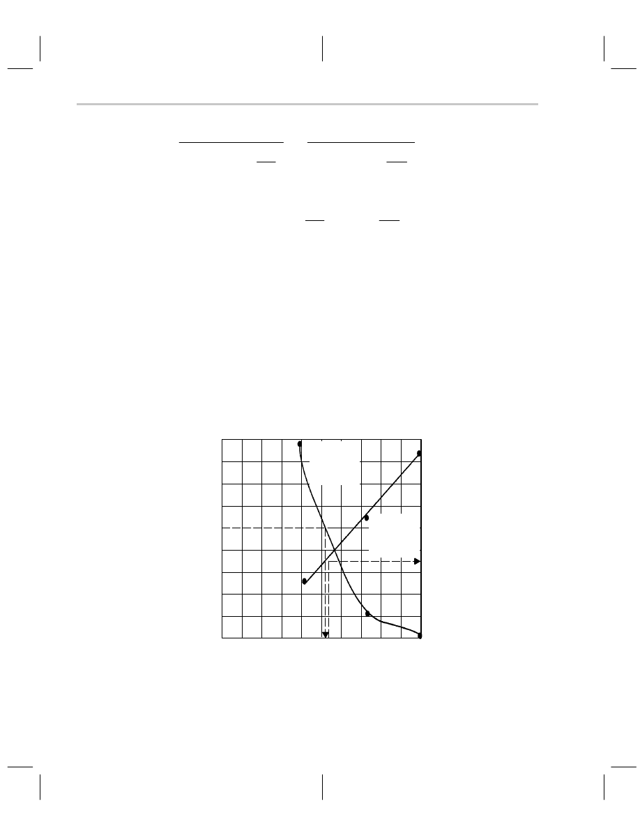
is to use graphical techniques. The graph shown in Fig-
ure 8–7 is a plot of the typical 300-MHz CFA data given in Table 8–1.
100
0
200 300
600
500
400
700 800
GAIN and BANDWIDTH
vs
FEEDBACK RESISTOR
7
5
3
1
6
4
2
Feedback Resistor –
Ω
Gain
9
8
900
10
1k
130
120
110
100
90
80
70
60
50
40
Bandwidth
–
MHz
Gain
vs.
Feedback
Resistance
Bandwidth
vs.
Feedback
Resistance
Figure 8–7. Plot of CFA R
F
, G, and BW
Stability and Input Capacitance
8-11
Current-Feedback Op Amp Analysis
Table 8–1. Data Set for Curves in Figure 8–7
GAIN (ACL)
RF (
Ω
)
BANDWIDTH (MHz)
+ 1
1000
125
+ 2
681
95
+ 10
383
65
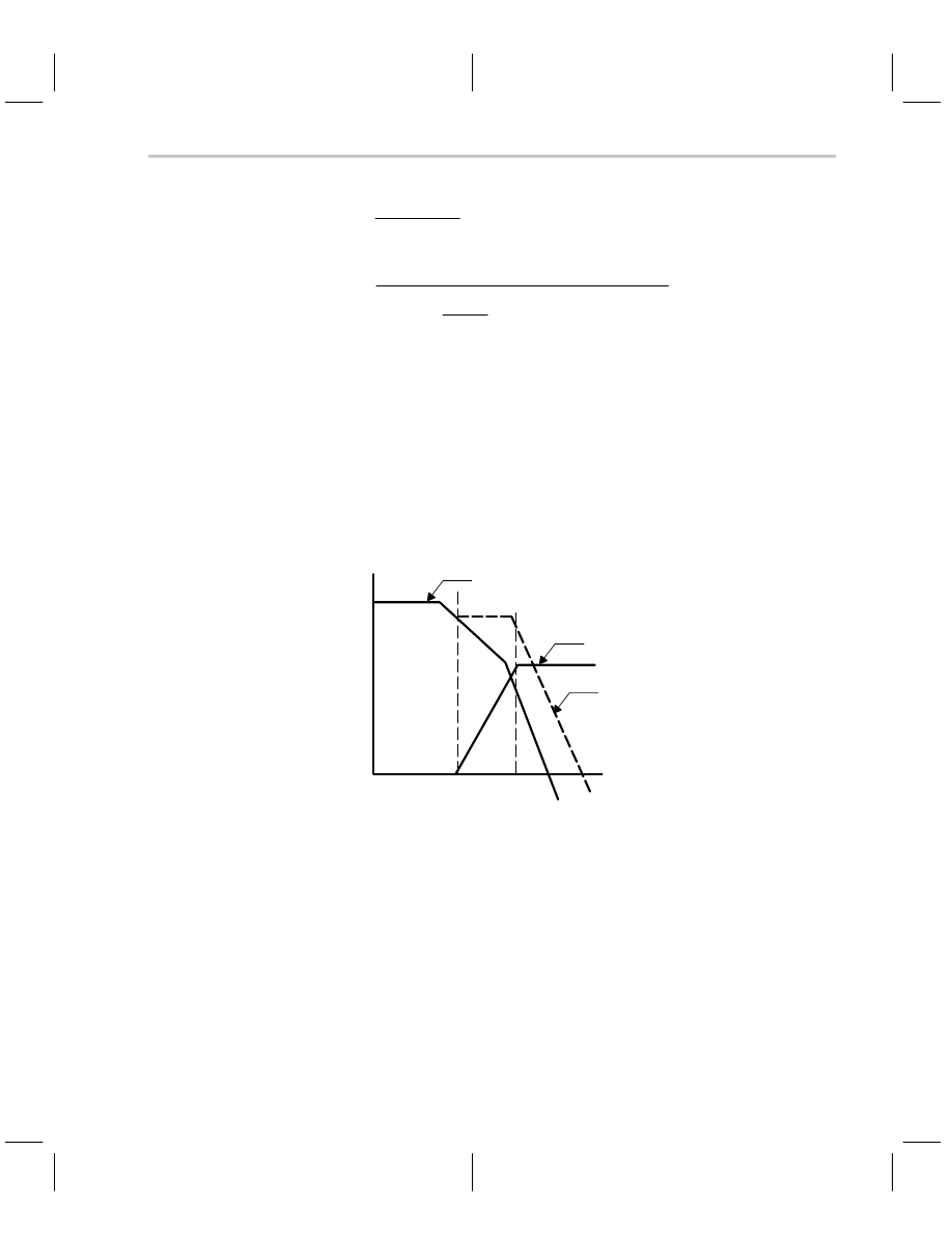
Enter the graph at the new gain, say A
CL
= 6, and move horizontally until you reach the
intersection of the gain versus feedback resistance curve. Then drop vertically to the re-
sistance axis and read the new value of R
F
(500
Ω
in this example). Enter the graph at
the new value of R
F
, and travel vertically until you intersect the bandwidth versus feedback
resistance curve. Now move to the bandwidth axis to read the new bandwidth (75 MHz
in this example). As a starting point you should expect to get approximately 75 MHz BW
with a gain of 6 and R
F
= 500
Ω
. Although this technique yields more reliable solutions
than Equation 8–27 does, op amp peculiarities, circuit board stray capacitances, and wir-
ing make extensive testing mandatory. The circuit must be tested for performance and
stability at each new operating point.
8.8
Stability and Input Capacitance
When designer lets the circuit board introduce stray capacitance on the inverting input
node to ground, it causes the impedance Z
G
to become reactive. The new impedance,
Z
G
, is given in Equation 8–28, and Equation 8–29 is the stability equation that describes
the situation.
(8–28)
Z
G
+
R
G
1
)
R
G
C
G
s
(8–29)
A
b +
Z
Z
B
)
Z
F
Z
2
G
)
Z
B
Z
G
(8–30)
A
b +
Z
R
F
ǒ
1
)
R
B
R
F
ø
R
G
Ǔ
ǒ
1
)
R
B
ø
R
F
ø
R
G
C
G
s
Ǔ
Equation 8–29 is the stability equation when Z
G
consists of a resistor in parallel with stray
capacitance between the inverting input node and ground. The stray capacitance, C
G
, is
a fixed value because it is dependent on the circuit layout. The pole created by the stray
capacitance is dependent on R
B
because it dominates R
F
and R
G
. R
B
fluctuates with
manufacturing tolerances, so the R
B
C
G
pole placement is subject to IC manufacturing tol-
erances. As the R
B
C
G
combination becomes larger, the pole moves towards the zero fre-
Stability and Feedback Capacitance
8-12
quency axis, lowering the circuit stability. Eventually it interacts with the pole contained
in Z, 1/
τ
2
, and instability results.
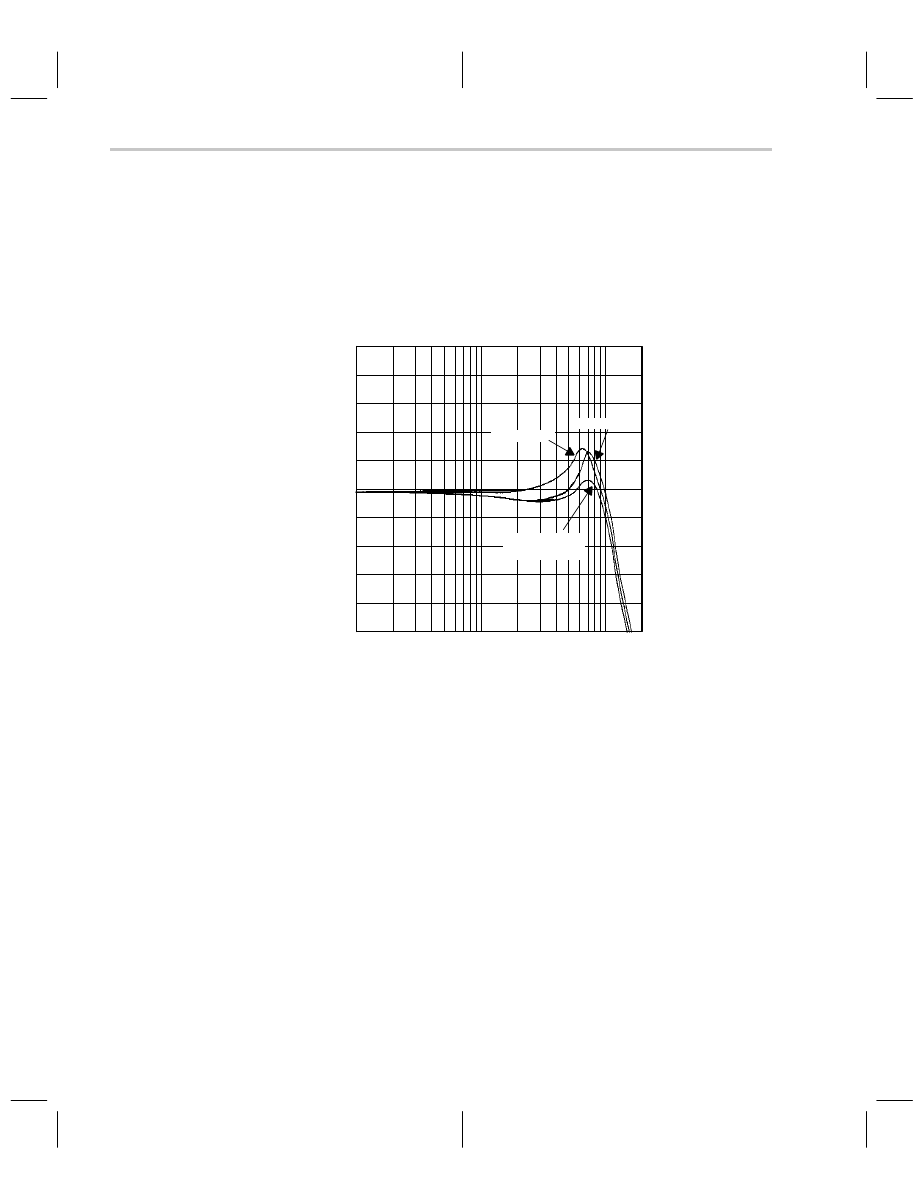
The effects of stray capacitance on CFA closed-loop performance are shown in Figure
8–8.
1
10
100
Amplitude (3 dB/div)
f – Frequency – MHz
AMPLITUDE
vs
FREQUENCY
No Stray
Capacitance
CF = 2 pF
CIN = 2 pF
Figure 8–8. Effects of Stray Capacitance on CFAs
Notice that the introduction of C
G
causes more than 3 dB peaking in the CFA frequency
response plot, and it increases the bandwidth about 18 MHz. Two picofarads are not a
lot of capacitance because a sloppy layout can easily add 4 or more picofarads to the cir-
cuit.
8.9
Stability and Feedback Capacitance
When a stray capacitor is formed across the feedback resistor, the feedback impedance
is given by Equation 8–31. Equation 8–32 gives the loop gain when a feedback capacitor
has been added to the circuit.
Compensation of CF and CG
8-13
Current-Feedback Op Amp Analysis
(8–31)
Z
F
+
R
F
1
)
R
F
C
F
s
(8–32)
A
b +
Z
ǒ
1
)
R
F
C
F
s
Ǔ
R
F
ǒ
1
)
R
B
R
F
ø
R
G
Ǔ
ǒ
1
)
R
B
ø
R
F
ø
R
G
C
F
s
Ǔ
This loop gain transfer function contains a pole and zero, thus, depending on the pole/zero
placement, oscillation can result. The Bode plot for this case is shown in Figure 8–9. The
original and composite curves cross the 0-dB axis with a slope of –40 dB/decade, so either
curve can indicate instability. The composite curve crosses the 0-dB axis at a higher fre-
quency than the original curve, hence the stray capacitance has added more phase shift
to the system. The composite curve is surely less stable than the original curve. Adding
capacitance to the inverting input node or across the feedback resistor usually results in
instability. R
B
largely influences the location of the pole introduced by C
F
, thus here is
another case where stray capacitance leads to instability.
0
POLE/ZERO Curve
Composite Curve
LOG(f)
AMPLITUDE (dB )
Ω
20LOGIZI – 20LOGIZF(1 + ZB/ZFIIZG)I
fZ
fP
Figure 8–9. Bode Plot with C
F
Figure 8–8 shows that C
F
= 2 pF adds about 4 dB of peaking to the frequency response
plot. The bandwidth increases about 10 MHz because of the peaking. C
F
and C
G
are the
major causes of overshoot, ringing, and oscillation in CFAs, and the circuit board layout
must be carefully done to eliminate these stray capacitances.
8.10 Compensation of C
F
and C
G
When C
F
and C
G
both are present in the circuit they may be adjusted to cancel each other
out. The stability equation for a circuit with C
F
and C
G
is Equation 8–33.

Summary
8-14
(8–33)
A
b +
Z
ǒ
1
)
R
F
C
F
s
Ǔ
R
F
ǒ
1
)
R
B
R
F
ø
R
G
Ǔ
ǒ
R
B
ø
R
F
ø
R
G
ǒ
C
F
)
C
G
Ǔ
s
)
1
Ǔ
If the zero and pole in Equation 8–33 are made to cancel each other, the only poles re-
maining are in Z. Setting the pole and zero in Equation 8–33 equal yields Equation 8–34
after some algebraic manipulation.
(8–34)
R
F
C
F
+
C
G
ǒ
R
G
ø
R
B
Ǔ
R
B
dominates the parallel combination of R
B
and R
G
, so Equation 8–34 is reduced to
Equation 8–35.
(8–35)
R
F
C
F
+
R
B
C
G
R
B
is an IC parameter, so it is dependent on the IC process. R
B
it is an important IC param-
eter, but it is not important enough to be monitored as a control variable during the
manufacturing process. R
B
has widely spread, unspecified parameters, thus depending
on R
B
for compensation is risky. Rather, the prudent design engineer assures that the cir-
cuit will be stable for any reasonable value of R
B
, and that the resulting frequency re-
sponse peaking is acceptable.
8.11 Summary
Constant gain-bandwidth is not a limiting criterion for the CFA, so the feedback resistor
is adjusted for maximum performance. Stability is dependent on the feedback resistor;
as R
F
is decreased, stability is decreased, and when R
F
goes to zero the circuit becomes
unstable. As R
F
is increased stability increases, but the bandwidth decreases.
The inverting input impedance is very high, but the noninverting input impedance is very
low. This situation precludes CFAs from operation in the differential amplifier configura-
tion. Stray capacitance on the inverting input node or across the feedback resistor always
leads to peaking, usually to ringing, and sometimes to oscillations. A prudent circuit de-
signer scans the PC board layout for stray capacitances, and he eliminates them. Bread-
boarding and lab testing are a must with CFAs. The CFA performance can be improved
immeasurably with a good layout, good decoupling capacitors, and low inductance com-
ponents.

IMPORTANT NOTICE
Texas Instruments Incorporated and its subsidiaries (TI) reserve the right to make corrections, modifications,
enhancements, improvements, and other changes to its products and services at any time and to discontinue
any product or service without notice. Customers should obtain the latest relevant information before placing
orders and should verify that such information is current and complete. All products are sold subject to TI’s terms
and conditions of sale supplied at the time of order acknowledgment.
TI warrants performance of its hardware products to the specifications applicable at the time of sale in
accordance with TI’s standard warranty. Testing and other quality control techniques are used to the extent TI
deems necessary to support this warranty. Except where mandated by government requirements, testing of all
parameters of each product is not necessarily performed.
TI assumes no liability for applications assistance or customer product design. Customers are responsible for
their products and applications using TI components. To minimize the risks associated with customer products
and applications, customers should provide adequate design and operating safeguards.
TI does not warrant or represent that any license, either express or implied, is granted under any TI patent right,
copyright, mask work right, or other TI intellectual property right relating to any combination, machine, or process
in which TI products or services are used. Information published by TI regarding third–party products or services
does not constitute a license from TI to use such products or services or a warranty or endorsement thereof.
Use of such information may require a license from a third party under the patents or other intellectual property
of the third party, or a license from TI under the patents or other intellectual property of TI.
Reproduction of information in TI data books or data sheets is permissible only if reproduction is without
alteration and is accompanied by all associated warranties, conditions, limitations, and notices. Reproduction
of this information with alteration is an unfair and deceptive business practice. TI is not responsible or liable for
such altered documentation.
Resale of TI products or services with statements different from or beyond the parameters stated by TI for that
product or service voids all express and any implied warranties for the associated TI product or service and
is an unfair and deceptive business practice. TI is not responsible or liable for any such statements.
Mailing Address:
Texas Instruments
Post Office Box 655303
Dallas, Texas 75265
Copyright
2001, Texas Instruments Incorporated
Wyszukiwarka
Podobne podstrony:
więcej podobnych podstron