Description
The CXA1645P/M is an encoder IC that converts
analog RGB signals to a composite video signal. This
IC has various pulse generators necessary for
encoding. Composite video outputs and Y/C outputs for
the S terminal are obtained just by inputting composite
sync, subcarrier and analog RGB signals.
It is best suited to image processing of personal
computers and video games.
Features
• Single 5V power supply
• Compatible with both NTSC and PAL systems
• Built-in 75
Ω
drivers
(RGB output, composite video output, Y output, C
output)
• Both sine wave and pulse can be input as a
subcarrier.
• Built-in band pass filter for the C signal and delay
line for the Y signal
• Built-in R-Y and B-Y modulator circuits
• Built-in PAL alternate circuit
• Burst flag generator circuit
• Half H killer circuit
Applications
Image processing of video games and personal
computers
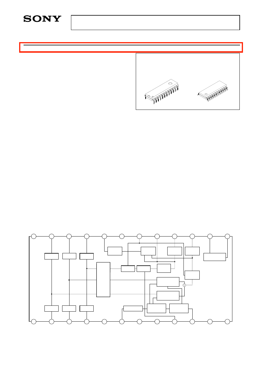
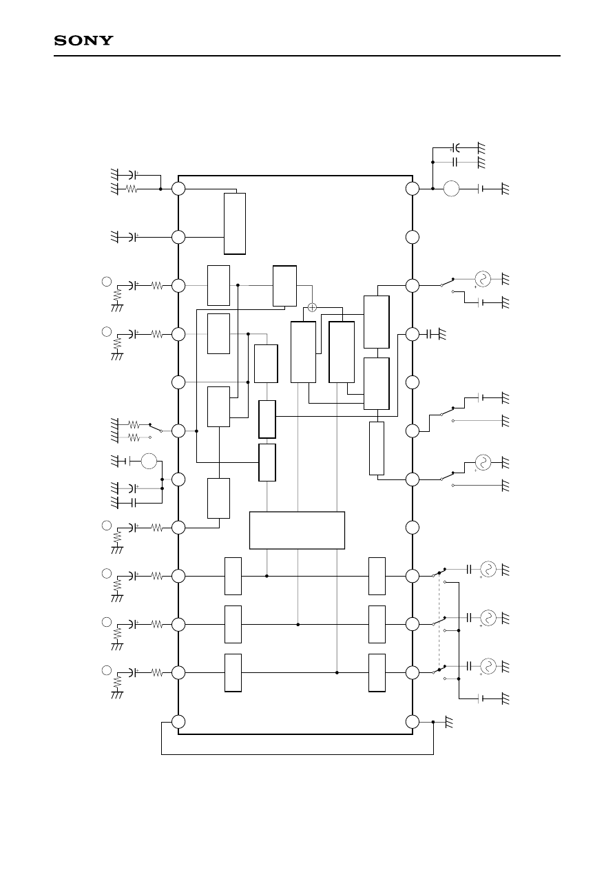
Block Diagram and Pin Configuration
Structure
Bipolar silicon monolithic IC
Absolute Maximum Ratings
• Supply voltage
V
CC
14
V
• Operating temperature Topr
–20 to +75
°C
• Storage temperature
Tstg
–65 to +150
°C
• Allowable power
P
D
CXA1645P 1250 mW
dissipation
CXA1645M 780 mW
Recommended Operating Condition
Supply voltage
V
CC
1, 2 5.0 ± 0.25
V
– 1 –
CXA1645P/M
E93411A41-ST
RGB Encoder
Sony reserves the right to change products and specifications without prior notice. This information does not convey any license by
any implication or otherwise under any patents or other right. Application circuits shown, if any, are typical examples illustrating the
operation of the devices. Sony cannot assume responsibility for any problems arising out of the use of these circuits.
24 pin DIP (Plastic)
24 pin SOP (Plastic)
BPF
PHASE
SHIFTER
R-Y
Modulator
B-Y
Modulator
PULSE
GEN
VIDEO
OUT
75
DRIVER
75
DRIVER
REGULATOR
SYNC
ADD
CLAMP
DELAY
Y/C
MIX
MATRIX
R-OUT
G-OUT
B-OUT
CLAMP
CLAMP
CLAMP
SIN-PULSE
2
3
4
5
1
8
9
6
7
11
12
10
15
16
17
13
14
18
19
20
21
22
23
24
SYNCIN
YCLPC
BFOUT
NPIN
SCIN
BIN
GIN
RIN
GND1
NC
V
CC
1
NC
COUT
YOUT
YTRAP
FO
V
CC
2
BOUT
GOUT
ROUT
GND2
V
REF
I
REF
CVOUT
For the availability of this product, please contact the sales office.
– 2 –
CXA1645P/M
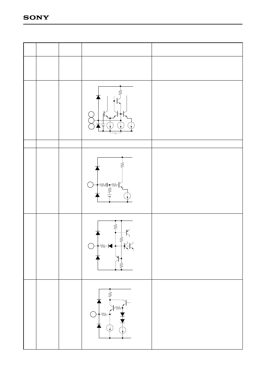
Pin Description
∗
Externally applied voltage
100µ
GND1
V
CC
1
I
CLP
180µ
100µ
2
3
4
Pin
No.
Symbol
Pin voltage
1
GND1
0V
∗
2
3
4
RIN
GIN
BIN
5
NC
6
SCIN
—
7
NPIN
1.7V
8
BFOUT
H : 3.6V
L : 3.2V
Black level
when
clamped
2.0V
Equivalent circuit
Description
Ground for all circuits other than RGB,
composite video and Y/C output circuits.
The leads to GND2 should be as short and
wide as possible.
Subcarrier input.
Input 0.4 to 0.5Vp-p sine wave or pulse.
Refer to Notes on Operation, Nos. 3 and 5.
Pin for switching between NTSC and PAL
modes
NTSC: V
CC
, PAL: GND
BF pulse monitoring output. Incapable of
driving a 75
Ω
load.
Analog RGB signal inputs. Input
100%, = 1Vp-p (max.). To minimize clamp
error, input at as low impedance as
possible.
I
CLP
turns ON only in the burst flag period.
NO CONNECTION
100µ
GND1
V
CC
1
2.5V
20k
20k
20P
129
6
GND1
V
CC
1
32k
68k
80k
3k
7
GND1
V
CC
1
25µ
129
8
25µ
– 3 –
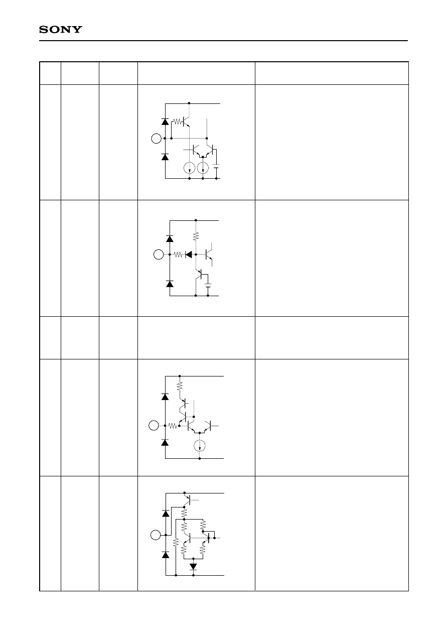
CXA1645P/M
Pin
No.
Symbol
Pin voltage
9
YCLPC
2.5V
10
SYNC
IN
12
V
CC
1
5.0V
∗
13
I
REF
2.0V
14
V
REF
4.0V
2.2V
Equivalent circuit
Description
Pin to determine the Y signal clamp time
constant.
Connect to GND via a 0.1µF capacitor.
Power supply for all circuits other than RGB,
composite video and Y/C output circuits.
Refer to Notes on Operation. Nos. 4 and 10.
Pin to determine the internal reference
current.
Connect to GND via a 47k
Ω
resistor.
Internal reference voltage.
Connect a decoupling capacitor of
approximately 10µF.
Refer to Notes on Operation, Nos. 4 and 7.
Composite sync signal input. Input TTL-
level voltages.
L (
≤
0.8V): SYNC period
H (
≥
2.0V)
1.6V
GND1
V
CC
1
5µ
9
129
GND1
V
CC
1
2.2V
4k
40k
10
GND1
V
CC
1
50µ
129
13
GND1
V
CC
1
14
– 4 –
CXA1645P/M
Pin
No.
Symbol
Pin voltage
15
COUT
2.2V
16
YOUT
17
YTRAP
Black level
1.6V
18
FO
2.0V
Black level
1.3V
Equivalent circuit
Description
Chroma signal output. Capable of driving a
75
Ω
load.
Refer to Notes on Operation, Nos. 6 and 9.
Pin for reducing cross color caused by the
subcarrier frequency component of the Y
signal. When the CVOUT pin is in use,
connect a capacitor or a capacitor and an
inductor in series between YTRAP and
GND. Decide capacitance and inductance,
giving consideration to cross color and the
required resolution.
No influence on the YOUT pin.
Refer to Notes on Operation, No. 8.
Internal filter fo adjustment pin.
Connect to GND via the following resistor
according to the NTSC or PAL mode.
NTSC: 20k
Ω
(±1%)
PAL : 16k
Ω
(±1%)
Y signal output. Capable of driving a 75
Ω
load.
Refer to Notes on Operation, Nos. 6 and 9.
10k
GND2
V
CC
2
15
20k
600µ
V
CC
1
10k
GND2
V
CC
2
20k
600µ
V
CC
1
16
GND1
V
CC
1
1.5k
8.5k
0.5P
17
Input resistance 1.5k
Ω
GND1
V
CC
1
129
50µ
18
– 5 –
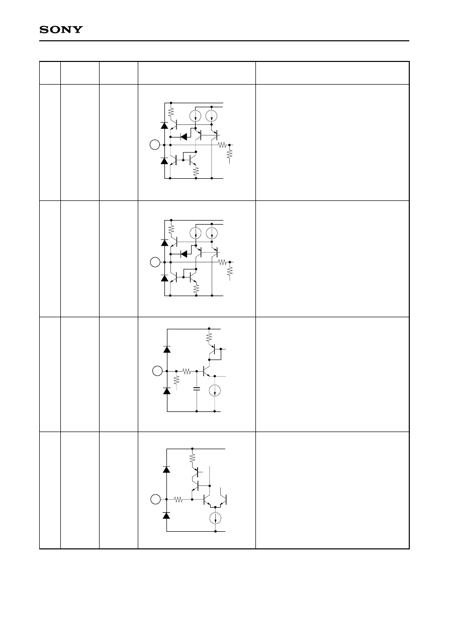
CXA1645P/M
Pin
No.
Symbol
Pin voltage
19
V
CC
2
5.0V
∗
20
CVOUT
21
22
23
BOUT
GOUT
ROUT
Black level
1.7V
24
GND2
0V
∗
Black level
1.2V
Equivalent circuit
Description
Power supply for RGB, composite video and
Y/C output circuits. Decouple this pin with a
large capacitor of 10µF or above as a high
current flows.
Refer to Notes on Operation, Nos. 4 and 10.
Analog RGB signal outputs. Capable of
driving a 75
Ω
load.
Refer to Notes on Operation, Nos. 6 and 9.
Ground for RGB, composite video and Y/C
output circuits. The leads to GND1 should
be as short and wide as possible.
Composite video signal output. Capable of
driving a 75
Ω
load.
Refer to Notes on Operation, Nos. 6 and 9.
10k
GND2
V
CC
2
20k
600µ
V
CC
1
20
GND2
V
CC
2
500µ
V
CC
1
5.5k
200µ
GND1
21
22
23
– 6 –
CXA1645P/M
Electrical Characteristics
(Ta = 25°C, V
CC
= 5V, See the Electrical Characteristics Measurement Circuit.)
Item
Symbol
S1
Current
consumption 1
Current
consumption 2
RGB output
voltage
(R, G, BOUT)
I
CC
1
I
CC
2
S2
S3
S4
S5
RIN
GIN
BIN
SCIN NPIN
SYNC
IN
FO
Measu
rement
point
2V
Measurement
Conditions
Min.
Typ.
Max.
Unit
SG4 5V SG5 20k
I
CC
1
I
CC
2
No input signal,
SG5: CSYNC
TTL level,
SG4: SIN
wave
3.58MHz
0.5Vp-p
Fig. 1
SG1 to SG3:
DC direct
coupling 2.5V
DC
,
1.0Vp-p
f = 200kHz
Pin 9 = Clamp
voltage
Fig. 2
31
12
mA
RGB output
frequency
characteristics
V
O
(R)
V
O
(G)
V
O
(B)
f
C
(R)
f
C
(G)
f
C
(B)
SG1
SG2
SG3
SG1
SG2
SG3
2V
2V
D
F
E
D
F
E
0.64
0.71
0.78
Vp-p
–3.0
dB
SG1 to SG3:
DC direct
coupling 2.5V
DC
,
1.0Vp-p
f = 200kHz/5MHz
Pin 9 = Clamp
voltage
Fig. 3
SG1 to SG3:
100% color bar
input,
1.0Vp-p (Max.)
SG5: CSYNC
TTL level
Fig. 4
(YOUT & CVOUT)
Output sync level
R100%: Y level
G100%: Y level
B100%: Y level
White 100%: Y level
V
O
(YS1/2)
V
O
(YR1/2)
V
O
(YG1/2)
V
O
(YB1/2)
V
O
(YW1/2)
Output frequency
characteristics
f
C
(Y1/2)
SG1
to
SG3
0V
5V SG5 20k
SG1
to
SG3
0V
5V
2V
20k
B/C
SG1 to SG3:
DC direct
coupling 2.5V
DC
,
1.0Vp-p
f = 200kHz/5MHz
Pin 9 = Clamp voltage
Fig. 3
0.26
0.17
0.35
0.065
0.6
0.29
0.21
0.42
0.08
0.71
0.33
0.26
0.49
0.095
0.82
Vp-p
V
V
V
V
–3.0
dB
∗
Clamp voltage: voltage appearing at Pin 9 when CSYNC is input.
– 7 –
CXA1645P/M
SG1 to SG3:
No signal,
SG4:
SIN wave,
3.58MHz
0.5Vp-p
SG5:
CSYNC
TTL level
3.58MHz component
measured. Fig. 6
SG1 to SG3:
No signal,
SG4: SIN wave,
4.43MHz
0.5Vp-p
SG5: CSYNC
TTL level
Fig. 6
(COUT & CVOUT)
Burst level
R chroma ratio
R phase
G chroma ratio
G phase
B chroma ratio
B phase
Burst width
Burst position
Carrier leak
PAL burst
level ratio
PAL burst phase
V
O
(BN1/2)
R/BN1/2
θ
R1/2
G/BN1/2
θ
G1/2
B/BN1/2
θ
B1/2
t
W
(B)
1/2
t
D
(B)
1/2
V
L1/2
K (BP1/2)
θ
PAL1/2
θ
PAL1/2
SG1
to
SG3
SG4
5V SG5 20k
0.2
SG1
to
SG3
SG4
5V SG5 20k
SG1
to
SG3
SG4 GND SG5 16k
A/C
SG1 to SG3:
100% color bar
input,
1.0Vp-p (Max.)
SG4: SIN wave,
3.58MHz
0.5Vp-p
SG5: CSYNC
TTL level
Fig. 5
0.25
0.3
Vp-p
2.84
3.16
3.48
94
104
114
deg
2.65
2.95
3.25
231
241
251
deg
2.01
2.24
2.47
337
347
357
deg
2.5
2.75
3.2
µs
0.4
0.6
0.75
µs
20
mVp-p
0.9
1.0
1.1
125
135
145
deg
215
225
235
∗
Clamp voltage: voltage appearing at Pin 9 when CSYNC is input.
Item
Symbol
S1
S2
S3
S4
S5
RIN
GIN
BIN
SCIN NPIN
SYNC
IN
FO
Measu
rement
point
Measurement
Conditions
Min.
Typ.
Max.
Unit
– 8 –
CXA1645P/M
Electrical Characteristics Measurement Circuit
BPF
PHASE SHIFTER
R-Y Modulator
B-Y Modulator
PULSE
GEN
VIDEO
OUT
75
DRIVER
75
DRIVER
REGULATOR
SYNC ADD
CLAMP
DELAY
Y/C MIX
MATRIX
R-OUT
G-OUT
B-OUT
CLAMP
CLAMP
CLAMP
SIN-PULSE
S1
S1
S1
0.1µ
SG1
0.1µ
SG2
0.1µ
SG3
2V
SG1 to SG3 100% color bar (1Vp-p max.)
NC
NC
NC
NC
S2
S3
SG4 SIN 0.5Vp-p
PAL
NTSC
5V
S4
2V
SG5 CSYNC
0.1µ
5V
0.01µ
47µ
I
CC
1
2
3
4
5
1
8
9
6
7
11
12
10
5V
47µ
220µ
A
75
75
A
220µ
75
75
B
220µ
75
75
C
220µ
75
75
D
220µ
75
75
E
220µ
75
75
F
0.01µ
A
S5
NTSC
PAL
20k
16k
47k
0.1µ
10µ
15
16
17
13
14
18
19
20
21
22
23
24
I
CC
2
– 9 –
CXA1645P/M
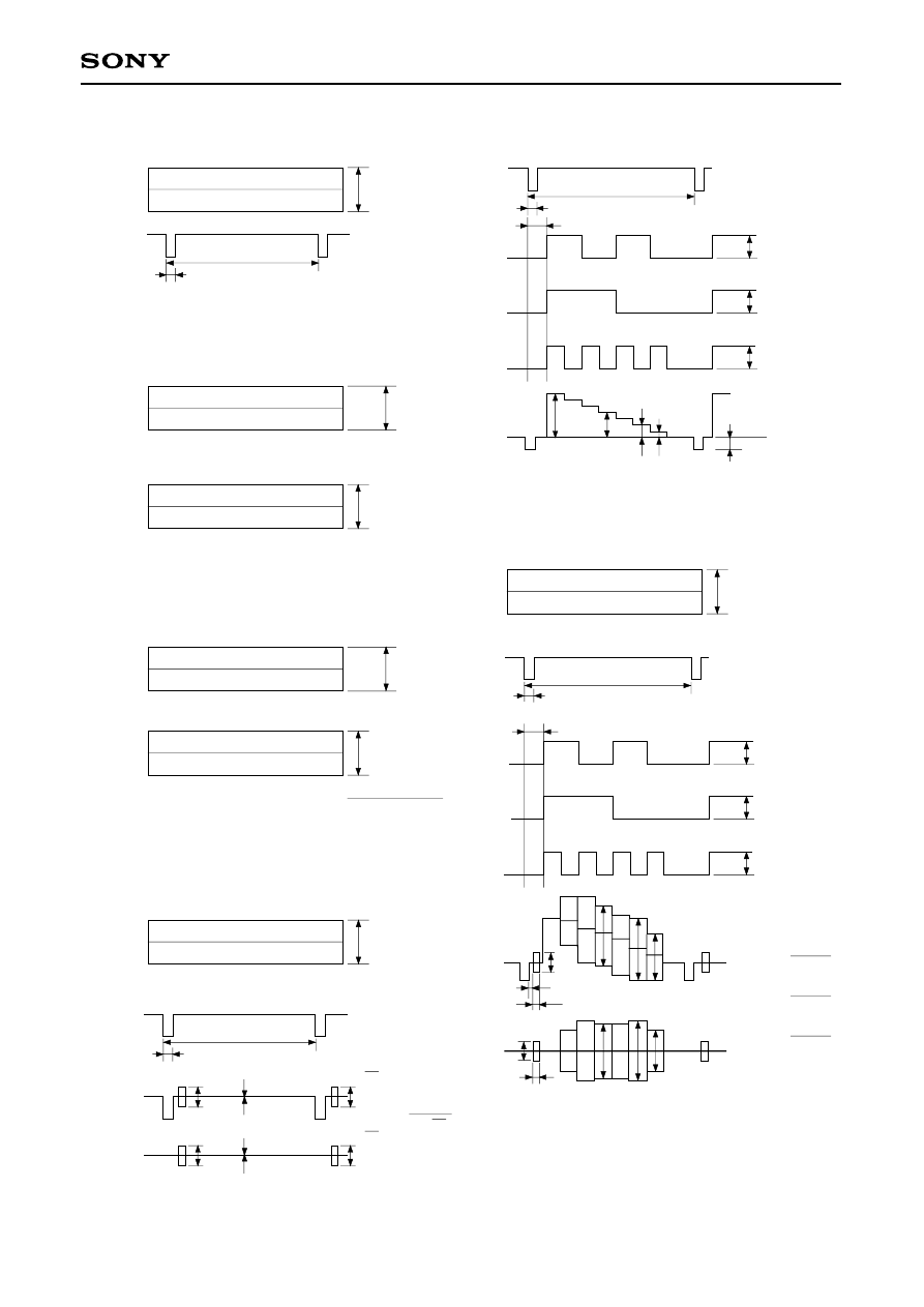
Measuring Signals and Output Waveforms
SG4
SCIN
SG5
SYNC
IN
64µs
4.5µs
2.0V
0.8V
0.5Vp-p
f = 3.58MHz
Fig. 1
Fig. 2
SG1 to 3
RIN
GIN
BIN
DEF point
ROUT
GOUT
BOUT
V
O
2.5V
1.0Vp-p
f = 200kHz
Fig. 3
SG1 to 3
RIN
GIN
BIN
DEF
BC point
ROUT
GOUT
BOUT
YOUT
CVOUT
V
O
2.5V
1.0Vp-p
f = 200kHz/5MHz
fc = 20log
Vo (5MHz)
Vo (200kHz)
Fig. 6
SG4
SCIN
SG4
SYNC
IN
C point
CVOUT
A point
COUT
Vo
(BN)
Vo
(BN)
V
L
V
L
4.5µs
64µs
0.5Vp-p
f = 3.58MHz/
4.43MHz
2.0V
0.8V
Vo
(BN)
Vo
(BN)
K (BP) =
Vo
(BN)
Vo
(BN)
SG5
SYNC
IN
SG1
RIN
SG2
GIN
SG3
BIN
BC point
YOUT
CVOUT
2.0V
0.8V
1.0Vp-p
1.0Vp-p
1.0Vp-p
Vo
(YS)
Vo
(YB)
Vo
(YR)
Vo
(YG)
Vo
(YW)
Fig. 4
64µs
4.5µs
10µs
Fig. 5
SG4
SCIN
SG5
SYNC
IN
SG1
RIN
SG2
GIN
SG3
BIN
0.5Vp-p
f = 3.58MHz
2.0V
0.8V
4.5µs
64µs
10µs
1.0Vp-p
1.0Vp-p
1.0Vp-p
C point
CVOUT
t
D (B)
A point
COUT
V
O (BN)
V
O (CG)
V
O (CR)
V
O (CB)
V
O (CG)
V
O (CR)
V
O (CB)
t
W (B)
V
O (BN)
t
W (B)
R/BN =
V
O (CR)
V
O (BN)
G/BN =
V
O (CG)
V
O (BN)
B/BN =
V
O (CB)
V
O (BN)
– 10 –
CXA1645P/M
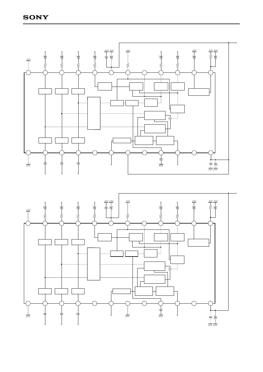
Application Circuit (NTSC mode)
Application Circuit (PAL mode)
BPF
PHASE
SHIFTER
R-Y
Modulator
B-Y
Modulator
PULSE
GEN
VIDEO
OUT
75
DRIVER
75
DRIVER
REGULATOR
SYNC
ADD
CLAMP
DELAY
Y/C
MIX
MATRIX
R-OUT
G-OUT
B-OUT
CLAMP
CLAMP
CLAMP
SIN-PULSE
0.1µ
NC
NC
NC
NC
0.1µ
0.01µ
47µ
+5V
47µ
220µ
75
220µ
75
220µ
75
220µ
75
220µ
75
220µ
75
R
OUT
0.01µ
20k
47k
0.1µ
10µ
15
16
17
13
14
18
19
20
21
22
23
24
G
OUT
B
OUT
CV
OUT
C
OUT
Y
OUT
B
IN
0.1µ
G
IN
0.1µ
R
IN
SCIN
SYNC
IN
2
3
4
5
1
8
9
6
7
11
12
10
V
CC
∗
1%
∗
Metal film resistor ±1%
BPF
PHASE
SHIFTER
R-Y
Modulator
B-Y
Modulator
PULSE
GEN
VIDEO
OUT
75
DRIVER
75
DRIVER
REGULATOR
SYNC
ADD
CLAMP
DELAY
Y/C
MIX
MATRIX
R-OUT
G-OUT
B-OUT
CLAMP
CLAMP
CLAMP
SIN-PULSE
0.1µ
NC
NC
NC
NC
0.1µ
0.01µ
47µ
+5V
47µ
220µ
75
220µ
75
220µ
75
220µ
75
220µ
75
220µ
75
R
OUT
0.01µ
16k
47k
0.1µ
10µ
15
16
17
13
14
18
19
20
21
22
23
24
G
OUT
B
OUT
CV
OUT
C
OUT
Y
OUT
B
IN
0.1µ
G
IN
0.1µ
R
IN
SCIN
SYNC
IN
2
3
4
5
1
8
9
6
7
11
12
10
V
CC
∗
1%
∗
Metal film resistor ±1%
Application circuits shown are typical examples illustrating the operation of the devices. Sony cannot assume responsibility for
any problems arising out of the use of these circuits or for any infringement of third party patent and other right due to same.
– 11 –
CXA1645P/M
Description of Operation
Analog RGB signals input from Pins 2, 3 and 4 are clamped in the clamping circuit and output from Pins 23,
22 and 21, respectively.
The matrix circuit performs operations on each input signal, generating luminance signal Y and color
difference signals R-Y and B-Y. The Y signal enters the delay line to adjust delay time with the color signal C.
Then, after addition of the CSYNC signal input from Pin 10, the Y signal is output from Pin 16.
A subcarrier input from Pin 6 is input to the phase shifter, where its phase is sfited 90°. Then, the subcarrier
is input to the modulators and modulated by the R-Y signal and the B-Y signal. Modulated subcarriers are
mixed, sent to the band pass filter to eliminate higher harmonic components and finally output from Pin 15 as
the C signal. At the same time, Y and C signals are mixed and output from Pin 20 as the composite video
signal.
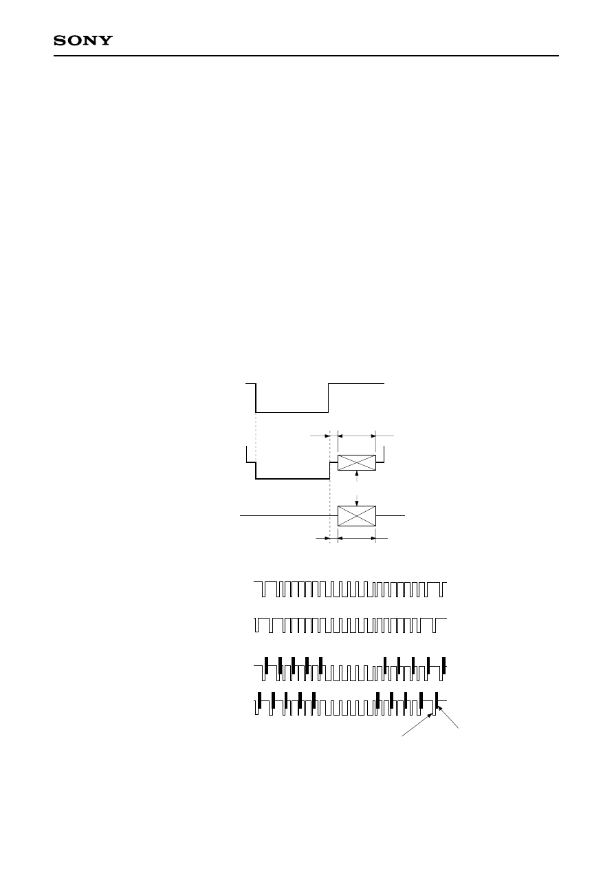
Burst Signal
The CXA1645P/M generates burst signals at the timing shown below according to the composite sync signal
input.
H synchronization
V synchronization
Burst signal
t
D (B)
t
W
(B)
t
D (B)
t
W (B)
SYNC
IN
(TTL level)
C VIDEO
OUT
COUT
Burst signal
Synchronizing signal
SYNC
IN
C VIDEO
OUT
ODD
EVEN
ODD
EVEN
– 12 –
CXA1645P/M
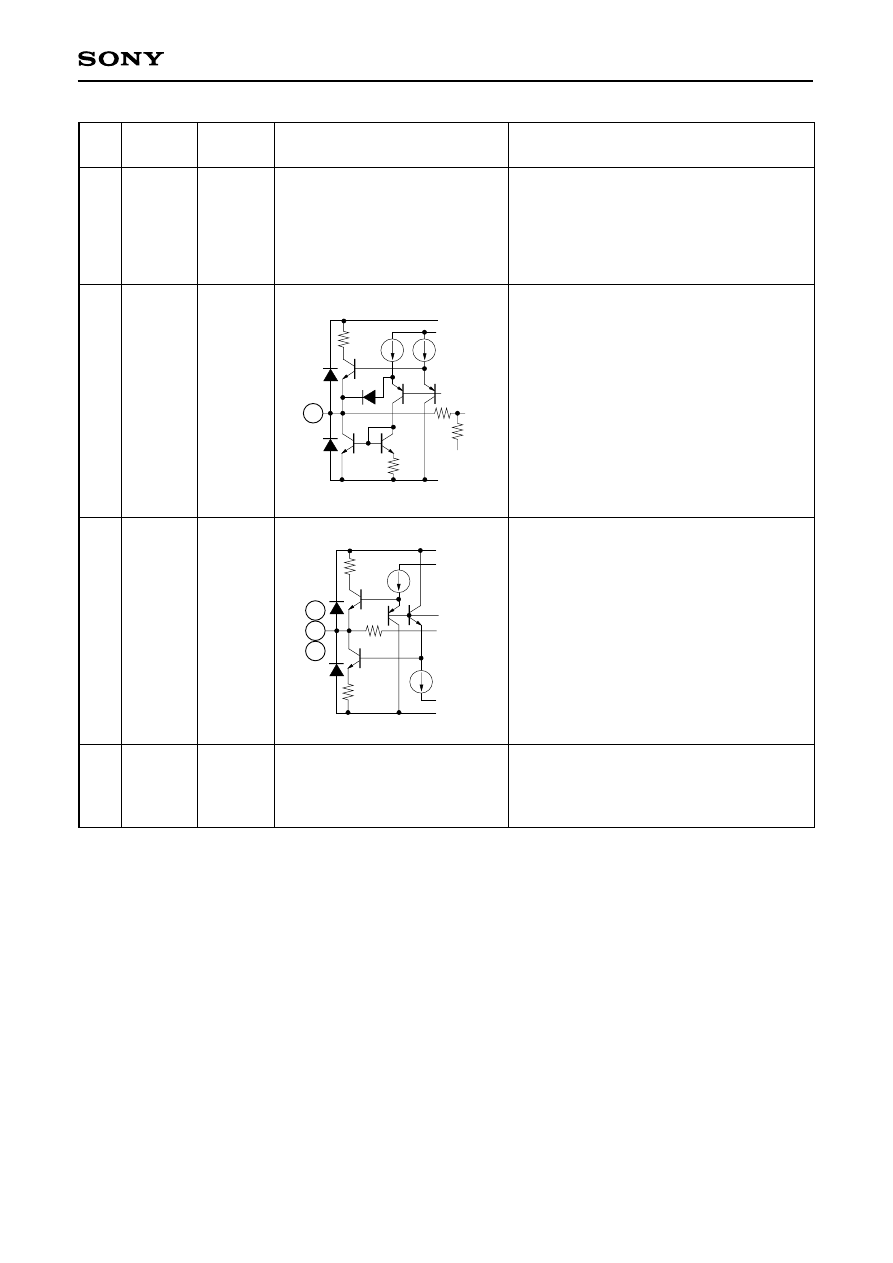
Notes on Operation
Be careful of the following when using the CXA1645P/M.
1. This IC is designed for image processing of personal computers and video games. When using the IC in
other video devices, make thorough investigations on image quality.
2. Be sure that analog RGB signals are input at 1.0Vp-p maximum and have low enough impedance. High
impedance may affect color saturation, hue, etc. Inputting RGB signals in excess of 1.3Vp-p may disable
the clamp operation.
3. The SC input (Pin 6) can be either a sine wave or a pulse in the range from 0.4 to 5.0Vp-p.
However, when a pulse is input, its phase may be shifted several degrees from that of the sine wave input.
In the IC, the SC input is biased to 1/2 V
CC
. Accordingly, when a 5.0Vp-p pulse is input and the duty factor
deviates from 50%, High- and Low-level pulse voltages may exceed V
CC
and GND in the IC, which causes
subcarrier distortion. In such a case, be very careful that the duty factor keeps to 50%.
4. When designing a printed circuit board pattern, pay careful attention to the routing of the V
CC
and GND
leads. To decouple the V
CC
and V
REF
pins, use tantalum, ceramic or other capacitors with good frequency
characteristics. Ground the capacitors by connections shown below as closely to each IC pin as possible.
Try to design the leads as short and wide as possible.
V
CC
1, V
REF
... GND1
V
CC
2
... GND2
Design the pattern so that V
CC
(or V
REF
) is connected to GND via a capacitor at the shortest distance.
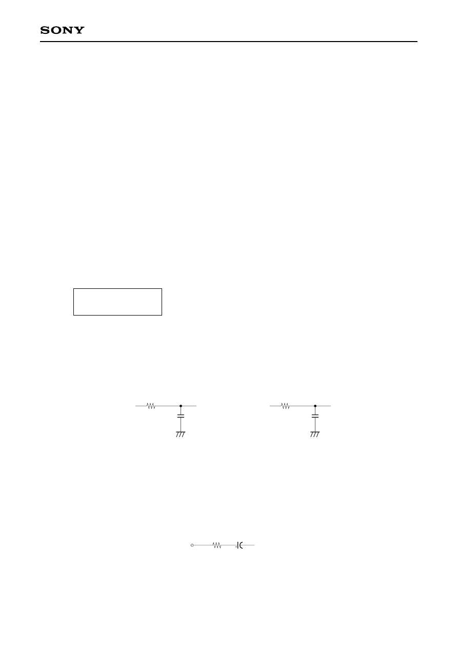
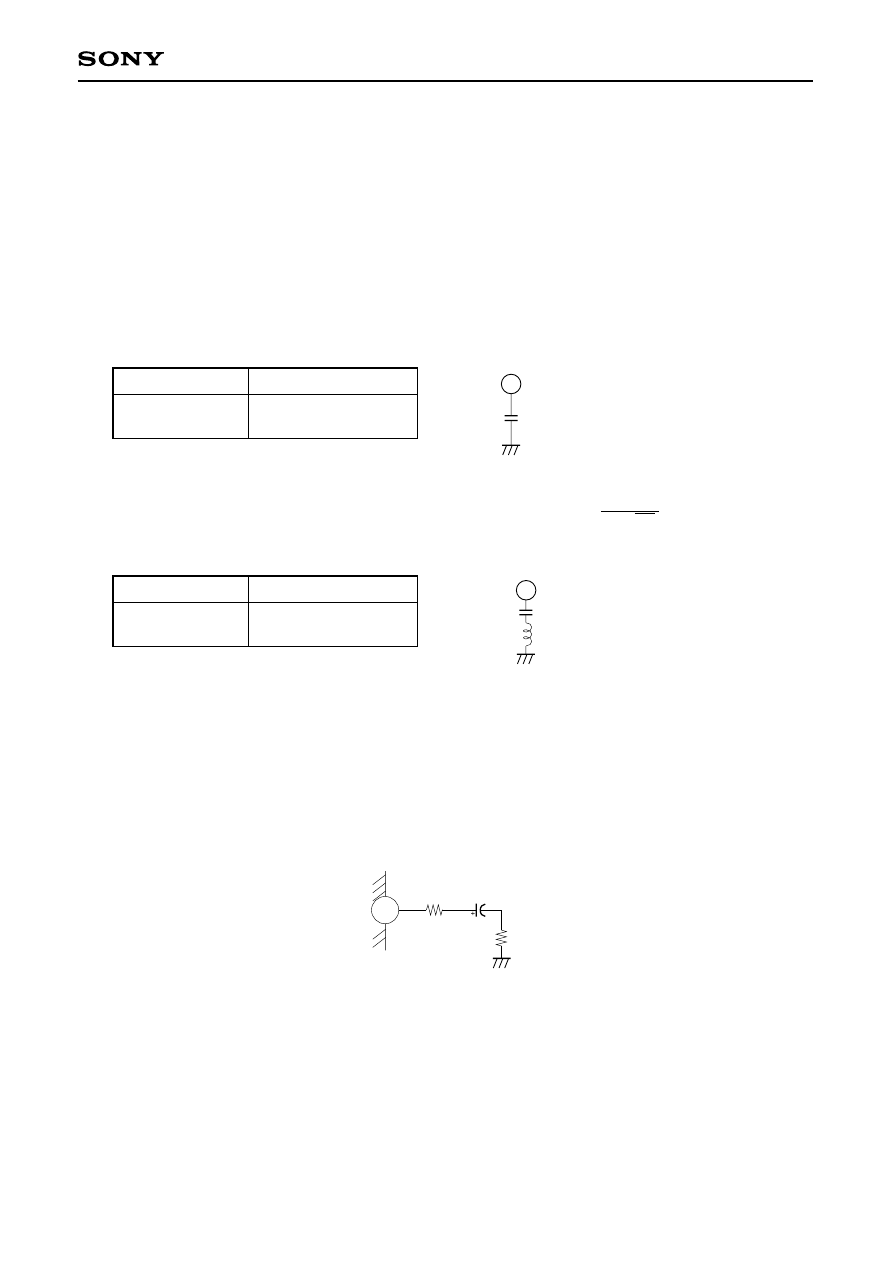
5. SC and SYNC input pulses
Attach a resistor and a capacitor to eliminate high-frequency components of SC (Figure A) and SYNC
(Figure B) before input.
Be careful not to input pulses containing high-frequency components. Otherwise, high-frequency
components may flow into V
CC
, GND and peripheral parts, resulting in malfunctions.
6. Connecting an external resistor to the 75
Ω
driver output pin
A capacitance of several dozen picofarads at each pin may start oscillation. To prevent oscillation, design
the pattern so that a 75
Ω
resistor is mounted near the pin (see Figure C).
When any of the 75
Ω
driver output pins is not in use, leave it unconnected and design the pattern so that
no parasitic capacitance is generated on the printed circuit board.
Fig. A
2.2k
5P
Fig. B
2.2k
47P
Fig. C
75
∗
∗
∗
Make these leads short.
– 13 –
CXA1645P/M
7. V
REF
pin (Pin 14)
Do not connect this pin to an external load that might cause AC signals to flow, which will cause IC
malfunctions. When connecting a DC load, make sure that the current flowing from this pin is kept below
2mA.
8. YTRAP pin (Pin 17)
There are the following two means of reducing cross color generated by subcarrier frequency components
contained in the Y signal.
(1)
Install a capacitor of 30 to 68pF between YTRAP and GND. Decide the capacitance by conducting image
evaluation, etc., giving consideration to both cross color and resolution.
Relations between capacitance and image quality are as follows:
(2)
Connect a capacitor C and an inductor L in series between YTRAP and GND. When the subcarrier
frequency is fo, the values C and L are determined by the equation fo = . Decide the values in
image evaluation, etc., giving consideration to both cross color and resolution.
Relations between inductor values and image quality are as follows:
For instance, L = 68µH and C = 28pF are recommended for NTSC. It is necessary to select an inductor L
with a sufficiently small DC resistance. Method (2) is more useful for achieving a higher resoluation than
method (1). When an even higher resolution is necessary, use of the S terminal (YOUT and COUT) is
recommended.
9. Driving COUT (Pin 15), YOUT (Pin 16), CVOUT (Pin 20), and B.G.R OUT (Pins 21, 22 and 23) outputs
In Pin Description, "Capable of driving a 75
Ω
load" means that the pin can drive a capacitor +75
Ω
+75
Ω
load shown in the figure below. In other words, the pin is capable of driving a 150
Ω
load in AC.
Keep in mind that the pin is incapable of driving a 150
Ω
load in DC load in DC direct coupling.
10. This IC employs a number of 75
Ω
driver pins, so oscillation is likely to occur when measures described in
Nos. 4 and 6 are not taken thoroughly. Be very careful of oscillation in printed circuit board design and
carry out thorough investigations in the actual driving condition.
Capacitance
30pF
←→
68pF
Cross color
Resolution
Large
←→
Small
High
←→
Low
17
C
Inductor value
Small
←→
Large
Cross color
Resolution
Large
←→
Small
High
←→
Low
17
C
L
1
2
π √
LC
75
Ω
220µF
75
Ω
PIN
– 14 –
CXA1645P/M
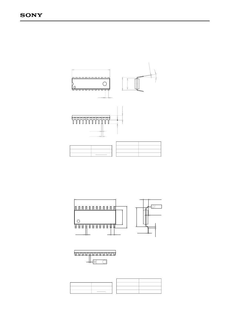
Package Outline
Unit: mm
CXA1645P
CXA1645M
24PIN DIP (PLASTIC) 400mil
30.2 – 0.1
+ 0.4
8.5 – 0.1
+ 0.3
0.25 – 0.05
+ 0.1
24
13
1
12
2.54
10.16
0° to 15°
3.7 – 0.1
+ 0.4
0.5 ± 0.1
1.2 ± 0.15
3.0 MIN
0.5 MIN
SONY CODE
EIAJ CODE
JEDEC CODE
PACKAGE STRUCTURE
PACKAGE MATERIAL
LEAD TREATMENT
LEAD MATERIAL
PACKAGE WEIGHT
EPOXY RESIN
SOLDER PLATING
COPPER / 42 ALLOY
DIP-24P-01
∗
DIP024-P-0400-A
2.0g
SONY CODE
EIAJ CODE
JEDEC CODE
M
PACKAGE STRUCTURE
MOLDING COMPOUND
LEAD TREATMENT
LEAD MATERIAL
PACKAGE WEIGHT
EPOXY/PHENOL RESIN
SOLDER PLATING
COPPER ALLOY / 42ALLOY
24PIN SOP (PLASTIC)
15.0 – 0.1
+ 0.4
1
12
13
24
1.27
0.45 ± 0.1
5.3 – 0.1
+ 0.3
7.9 ±
0.4
0.2 – 0.05
+ 0.1
0.5 ±
0.2
0.1 – 0.05
+ 0.2
0.15
1.85 – 0.15
+ 0.4
6.9
± 0.12
SOP-24P-L01
∗
SOP024-P-0300-A
0.3g
Wyszukiwarka
Podobne podstrony:
CXA1646,1767
więcej podobnych podstron