
Technical Note of LA76818 2001/02/08
1/46
LA76818 Application Note
Ver.e1(2001.1.18)
Table of Contents
TABLE OF CONTENTS...........................................................................................................................................1
T
HE
BUS C
ONTROL
F
UNCTIONS OF
LA76818 (T
ENTATIVE
).............................................................................2
PIN 1 (A
UDIO
O
UTPUT
)........................................................................................................................................12
P
IN
2 (FM O
UTPUT
)...............................................................................................................................................13
PIN 3 (IF AGC F
ILTER
)........................................................................................................................................14
PIN 4 (RF AGC OUTPUT)..................................................................................................................................15
PIN 5,6 (PIF AMP INPUT)..................................................................................................................................17
PIN 7 (IF GROUND) ............................................................................................................................................17
PIN 8 (IF V
CC
) .......................................................................................................................................................17
PIN 9 (FM FILTER) ..............................................................................................................................................18
PIN 10 (AFT OUTPUT).......................................................................................................................................19
PIN 11 (BUS DATA).............................................................................................................................................19
PIN 12 (BUS CLOCK).........................................................................................................................................20
PIN 13(ABL) ..........................................................................................................................................................20
PIN 14, 15, 16 (R, G, B INPUT).........................................................................................................................21
PIN 17(FAST BLANKING INPUT) ..................................................................................................................21
PIN 18(RGB V
CC
).................................................................................................................................................22
PIN 19, PIN
20, PIN 21(R, G, B OUTPUT) .....................................................................................................23
PIN 22(
FSC OUTPUT OR C
-
SYNC
.
OUTPUT
).........................................................................................................24
PIN 23 (VERTICAL OUTPUT)..........................................................................................................................24
PIN 24 (V RAMP ALC FILTER)........................................................................................................................25
PIN 25 (HORIZONTAL / BUS V
CC
).................................................................................................................26
PIN 26(AFC FILTER)...........................................................................................................................................26
PIN 27 (HORIZONTAL OUTPUT) ...................................................................................................................27
PIN 28 (FBP INPUT)............................................................................................................................................28
PIN29 (I
REFERENCE
)............................................................................................................................................29
PIN 31( CCD V
CC
)................................................................................................................................................30
PIN 32( CCD FILTER) .........................................................................................................................................31
PIN 33(CCD & DEFLECTION GDN) ..............................................................................................................31
PIN 36 (CHROMA APC2 FILTER)...................................................................................................................33
PIN 37(CLAMP FILTER) ....................................................................................................................................33
PIN 38(4.43MH
Z
CRYSTAL)..............................................................................................................................34
PIN 39(CHROME APC1 FILTER).....................................................................................................................34
PIN 40(SELECTED VIDEO OUTPUT) ...........................................................................................................35
PIN 41(V
IDEO
C
HROME
D
EFLECTION
GND).....................................................................................................35
PIN 42(EXT VIDEO INPUT & Y INPUT
IN
S-VHS MODE)......................................................................35
PIN 43(VIDEO CHROME DEFLECTION VCC)...........................................................................................35
PIN 44(INT. VIDEO INPUT & CHROME SIGNAL INPUT IN S-VHS MODE)....................................36
PIN 45(BLACK STRETCH FILTER)................................................................................................................36
PIN 46 (VIDEO OUTPUT)..................................................................................................................................37
PIN 47 (VCO F
ILTER
)...........................................................................................................................................37
PIN 48, 49 (VCO COIL).......................................................................................................................................38
PIN 50 (PIF APC FILTER) ..................................................................................................................................39
PIN 51 (EXT AUDIO INPUT)............................................................................................................................40
PIN 52 (SIF OUTPUT).........................................................................................................................................40
PIN 53 (SND APC FILTER)................................................................................................................................41
PIN 54 (SIF INPUT)..............................................................................................................................................41
S
TATUE
R
EGISTER OF
LA76818............................................................................................................................42
LA76818 P
IN
A
SSIGNMENT
.................................................................................................................................43
LA76818 B
US
C
ONTROL
R
ESISTOR
B
IT
A
LLOCATION
M
AP
...........................................................................44
Technical Note of LA76818 2001/02/08
2/46
The BUS Control Functions of LA76818 (Tentative)
Register Name
Bits
General Description
T Disable
1 bits Disable the Test SW & enable Audio / Video Mute SW
This is a Test Mode Switch, which is used in IC production (in case of using IC tester
for measuring).
*If the bit of BUS is set as ‘0’, it becomes Test Mode. Then the test functions below will
take active.
•
Vertical Test
•
E/W Test
•
Tint Test
•
Color Test
•
Drive Test
•
Contrast Test
Also, audio / video is muted forcedly.
*Usually, this bit is set as ‘1’ when the television is operating normally.
AFC Gain & gate
1
Select horizontal first
loop gain & H-sync gating on/off
This function is used for keeping the stability of H sync. signal when there is no input
signal or when a special VCR signal (VCR AGC Micro-vision) is input.
0
= Automatic mode
There is a gate signal for 1
st
AFC gain control and sync signal to protect them from
variety special signals and guarantee the stability of horizontal output in all our products
before. The level of the gain control can only be set as HIGH, MIDDLE & LOW.
When “no input signal” (conditions are: no V sync and ‘H LOCK’ is unlocked) is
detected, “LOW” mode will be set to keep the horizontal deflection stable so that the H
& V position of OSD will not be interrupted.
In addition, the improved operation of gain control and gating control in this IC
contribute to stabilize horizontal output of VCR signal in automatic mode.
1
= Enforce High Gain Mode (Gain = High, Gate = Non gate)
This mode is prior to pull-in operation, that’s why the stability is comparative weak.
This mode is used when tuning or some unexpected conditions.
H Freq.
6
Align ES Sample horizontal frequency
(MP is adjusted in the wafer line.)
Adjustment has done for mass production products. Although it’s no need any
adjustment at TV production line, set the register as “111111”. (But it needs adjustment
at engineering sample stage).
Audio Mute
1
Disable audio outputs
Mute the audio output.
0
= Mute OFF
1
= Mute ON
Technical Note of LA76818 2001/02/08
3/46
Video Mute
1
Disable video outputs
Mute the RGB output.(The blanking output level of RGB is about 1.6Vdc)
0
= Mute OFF
1
= Mute ON
H PHASE
5
Align sync to flyback phase
Adjust the center of H.
Sync Kill
1
Force free-run mode
Whatever there is a synchronization signal or not, the frequency of horizontal oscillator
is in free-run situation. Set this function in active if “no signal” is detected by CPU, then
the rolling of OSD can almost be reduced.
0
= TV operating mode
1
= Sync Kill mode
Vertical Size
7
Align vertical amplitude
Adjust the size of V.
V-sync Separation Up
1
Select vertical sync. separation sensitivity
Improved the sensitivity of the vertical separation circuit.
0
= Normal mode
1
= Sensitivity up mode
Vertical Kill
1
Disable vertical output
Defeat the vertical output. Please use this function when adjust RGB Bias.。
0
= TV operation mode
1
= Defeat the vertical output
V POSI ( Vertical DC )
7
Align vertical DC bias
Adjust the position of V
V LIN
( Vertical Linearity )
5
Align vertical linearity
Compensation for vertical linearity
Vertical S-Correction
5
Align vertical S-correction
Compensation for vertical S characteristic.
H BLK L
3
Left H-Blanking Control ( Width/Phase )
The blanking of the left side of screen can be adjusted
*The design of FBP input circuit become simple because of the blanking of screen can
be adjusted independently).
H BLK R
3
Right H-Blanking Control ( Width/Phase )
Technical Note of LA76818 2001/02/08
4/46
The blanking of the right side of screen can be adjusted
*The design of FBP input circuit become simple because of the blanking of screen can
be adjusted independently).
Vertical Size
Compensation
3
Align vertical size compensation
Compensate vertical size due to the variation of contrast.
Count Down Mode
3
Select vertical countdown mode
This function is used to switch 50Hz/60Hz mode and standard/non-standard mode of
countdown circuit.
* Switch for standard/non-standard mode
0** : Automatic discriminate standard/non-standard mode
1** : Non-standard mode
Standard mode:
Using the dividing pulse of V countdown to reset the countdown circuit. A stable
synchronization signal can be achieved because it is not interfered by the external
vertical trigger. It becomes standard mode if it is synchronize with the standard
signal(262.5H or 312.5H).
Non-standard mode:
Using external vertical trigger to reset countdown circuit. In this case, the stability of
the sync signal is depended on external signal. This mode is used when the sync signal
cannot achieved or the frequency of sync signal is not 262.5H or 312.5H.
*Switch for 50/60 mode
00
: Automatic discriminate 50Hz/60Hz mode
01
: 50Hz mode
10
: 60Hz mode
11
: 50/60Hz automatic discriminate mode
60Hz mode
: Vertical trigger is accepted during 225H〜297H
50Hz mode
: Vertical trigger is accepted during 288H〜357H
50Hz/60Hz automatic discriminate mode
: 50Hz/60Hz mode is selected
automatically.
Red Bias
8
Align Red OUT DC level
Green Bias
8
Align Green OUT DC level
Blue Bias
8
Align Blue OUT DC level
Adjust the DC (cutoff) level of RGB.
Red Drive
7
Align Red OUT AC level
Green Drive
4
Align Green OUT AC level
Blue Drive
7
Align Blue OUT AC level
Adjust the output gain of RGB.
Technical Note of LA76818 2001/02/08
5/46
Half Tone
2
Adjust half tone level
Adjust the half tone level
Half Tone ON/OFF
1
Half tone ON/OFF SW
0
= Half tone OFF
1
= Half tone ON
Blank Defeat
1
Disable RGB output blanking
Switch ON/OFF the H/V blanking of RGB output.
0
= blanking ON (Normally mode)
1
= blanking off
Sub Bias (sub-bright)
7
Align common RGB DC level
Sub-adjust the DC level of RGB output.
Even the setting of the RGB drive are different, the variation of the DC level of RGB
output can be adjusted to be same by this function.
Brightness Control
7
Customer brightness control
Control brightness.
Contrast Control
7
Customer contrast control
Control contrast
OSD Contrast Control
2
Align OSD AC level
Adjust the gain of OSD signal.
Coring Gain Select
2
Select Coring Gain
Select Coring Gain.
00= Coring OFF
01= Coring Gain1(minimum)
11= Coring Gain2(maximum)
Sharpness Control
5
Customer sharpness control
Control sharpness
Tint Control
7
Customer tint control
Control tint (operate only in NTSC system)
Color Control
7
Customer color control
Control color
Technical Note of LA76818 2001/02/08
6/46
Video SW
1
Video signal selector
The switch of Int./Ext . video input
0
= Internal
1
= External
Trap Test
3
Sound trap control for testing
Sound trap control.
Filter System
3
Select Y/C Filter mode
Select the trap frequency and the peaking frequency of color trap filter of Y.
・ 3.58MHz Trap Mode / peaking at 2.2MHz
・ 4.43MHz Trap Mode/ peaking at 2.7MHz
・ No trap (High band mode)/
・ 4.286MHz Trap Mode/ peaking at 2.3 MHz
Y Block
Chroma Block
0
3.58MHz Trap
3.58MHz unsymmetrical
1
3.58MHz Trap
3.58MHz symmetrical
2
4.43MHz Trap
4.43MHz unsymmetrical
3
4.43MHz Trap
4.43MHz symmetrical
4
No trap
3.58MHz unsymmetrical
5
No trap
3.58MHz symmetrical
6
No trap
4.43MHz unsymmetrical
7
No trap
4.43MHz symmetrical
8 ~ 15
4.286MHz Trap
4.43MHz symmetrical
The switch of chroma band-pass filter.
Unsymmetrical Mode
Symmetrical Mode
Gray Mode
1
Service Test Mode (White/Gray)
Switch to white level when Cross B/W is set as ‘10’ or ‘11’.
0
: White(100%)
1
: Gray (60%)
Cross B/W
2
Service Test Mode ( normal/Cross/Black/White)
It is possible to generate crosshatch, white level, black level pattern.
00
= TV operating mode
01
= Black pattern
10
= White pattern
11
= Crosshatch pattern
•
Set the Cross B/W function as “black pattern” and input a chroma signal, then a
differential RGB output can be achieved. (Switch on the BLK Defeat SW, the
blanking pulse can also be defeated.)
•
Set the Cross B/W function as “black pattern” and minimize color level, then the
DC level of RGB can be used for adjusting the cutoff of CRT.
Technical Note of LA76818 2001/02/08
7/46
CbCr IN
1
Select YcbCr Input or SECAM Input.
Select SECAM Input or YcbCr Input.
0 : SECAM
1 : CbCr
G-Y Angle
4
Select G-Y angle
Select the demodulation angle of G-Y.
0
= 240 deg.
1
= 253 deg.
Color Killer
Operational Point
Select
3
Select color killer operational level
Color killer operational point can be selected depend on the input signal (etc. RF input
or Y/C input).
000
= -30dB
111
= -40dB
VBLK SW
1
V blanking control SW
The SW of V blanking.
0
= video signal period 24H ~ 262H
1
= video signal period 29H ~ 257H
FBP Blanking OR SW
1
Select Horizontal blanking operation
The “OR” of the H blanking (produced inside IC) and external input FBP signal
0
= Horizontal blanking is created by the internal logic.
1
= Horizontal blanking is the “OR” of the FBP & internal logic.
Y APF Select
1
Select Chroma Trap ON/OFF.
Use YcbCr mode.
0 = Chroma Trap ON
1 = All Pass Filter mode(Chroma Trap OFF):YcbCr mode
Pre/Over-shoot
adjustment
2
Select pre-shoot width
This function can adjust the pre-shoot component of the Y signal.
Usually, over-shoot component will increase when signal is proceeded in the IC. This
will cause unbalance with the pre-shoot (peaking frequency). Therefore, this function
can
00
= Narrow
11
= Wide
Technical Note of LA76818 2001/02/08
8/46
White Peak Limiter
2
Select White Peak Limiter level.(with Defeat)
When there is a bright spot signal in a low APL picture, ABL/ ACL does not operate
and this will cause blooming problem. To avoid this, when APL is low, white peak
limiter will operate to cut the abnormal bright signal.
00 = WPL OFF
01 = WPL ON(High operating point)
11 = WPL ON(Low operating point)
Y Gamma start point
Select
2
Select Y Gamma start point.(with Defeat)
00 = Y Gamma OFF
01 = Y Gamma ON(High operating point)
11 = Y Gamma ON(Low operating point)
DC Restoration Select
2
Select luma DC restoration
When the Black Stretch function is used during Y signal processing, the pedestal level
will shift according to the APL of signal. Therefore, to avoid this problem, DC renewal
rate can be selected in this IC.
00
= 100%
01
= 107%
10
= 113%
11
= 129%
Black Stretch Start Point
Select(w/Defeat)
2
Select Black Stretch Start Point(w/Defeat).
Select Black Stretch Start Point(with Defeat).
00
= Black Stretch OFF
01
= Black Stretch ON(40IRE)
10 = Black Stretch ON(60IRE)
Black Stretch Gain
Select
2
Select black stretch gain
00
= MIN.
10
= MAX
Auto-Flesh
1
Enable auto- flesh function
Switch ON / OFF the automatic flesh function.
0
= OFF
1
= ON
The characteristic of Automatic Flesh(exclusive use for NTSC)
At the center point of tint、the axis of Flesh is 118 degree、and the maximum
compensation is about 10 degree (7〜20deg).
(Set this function off in PAL system.)
Technical Note of LA76818 2001/02/08
9/46
C Ext.
1
Selected-C In SW on
0
= select the chroma signal of internal composite video signal.
1
= select the chroma signal that input from pin 44.
C Bypass
1
Select chroma BPF bypass
Bypass switch of chroma band-pass filter.
1
= bypass ON
0
= bypass OFF
C Kill On
1
C Kill Mode ( 0: Enable Killer circuit )
Ever when the color control is minimized, but maybe there is still has little color left in
the picture. In this case, we can set Col_Kill as ‘1’ together with the minimum color
setting to get rid of the residual color.
0
= Automatic Mode (Normally using this mode when TV in operation)
1
= Enforce killer ON when color control is minimized.
C Kill Off
1
Disable Killer circuit ( for IC Test )
This mode is used when using IC tester for measurement.
1
: Test mode, in this case, killer circuit is not in operation.
0
: TV operating mode
Color System
3
Select Color System
The color system can be set to automatic mode (000/001) or manual mode (010〜111)
by CPU.
Setting of BUS bit:
000 = Automatic mode 1 PAL/NTSC/4.43NTSC(/SECAM)
001 = Automatic mode 2 PAL-M/PAL-N/NTSC
010 = PAL
011 = PAL-M
100 = PAL-N
101 = NTSC
110 = 4.43NTSC
111 = SECAM
Digital OSD
1
Select Digital OSD mode/Analogue OSD mode
0 = Analogue OSD mode(Clamp circuit ON).
1 = Digital OSD mode(Clamp circuit OFF)
Bright ABL Defeat
1
Disable brightness ABL
Bright ABL Threshold
3
Align brightness ABL threshold
Bright Mid Stop Defeat
1
Disable brightness mid stop
In order to make the design of TV chassis more easier, ABL(Auto Beam
Limiter)function can be controlled by BUS.
Bright ABL Defeat: The defeat SW of Brightness ABL
1
= ABL Defeat ON
Technical Note of LA76818 2001/02/08
10/ 46
0
= ABL Defeat OFF
Bright ABL Threshold: Adjust the start operating point of Brightness ABL
Bright Mid Stop Defeat: The defeat switch for the limit operation of brightness ABL by
brightness control
1
= Disable limit operation
0
= Enable limit operation
RGB Temp. SW
1
Select the temperature characteristics for RGB DC output.
0 = -1VBE.
1 = Flat
R/B Balance
4
R-Y/B-Y Gain Balance
Adjust the demodulation ratio of R-Y and B-Y.
R/B Angle
4
R-Y/B-Y Angle
Adjust the demodulation angle of R-Y and B-Y.
B-Y DC Level
4
B-Y DC Level ( White-Balance )
R-Y DC Level
4
R-Y DC Level ( White-Balance )
*Fine adjust the offset of the DC level (white balance) when switch PAL/SECAM
system. SECAM decoder is using external IC.
Audio SW
1
The switch of Int./Ext . audio input.
0
= Internal
1
= External
Volume Control
7
Customer volume control
Sound volume control (attenuation mode)
Maximum gain
= 0dB, step
= 0.5dB
Volume Filter Defeat
1
Disable volume DAC filter
In order to get rid of the “POP” noise which is caused by the DAC of volume control,
volume filter is built-in into the IC.
This filter is set ‘OFF’ when IC tester is used for measuring.
0
: TV operating mode
1
: Filter OFF
RF AGC Delay
6
Align RF AGC threshold
Adjust RF AGC Delay point
De-emphasis TC
1
Select De-emphasis Time Constant
Switch of De-emphasis time constant
0
= 50uS
1
= 75uS
Technical Note of LA76818 2001/02/08
11/46
VIF System SW
2
Select 38.0/38.9/45.75/58.75
IF frequency switch
00
= 38.0MHz
01 =38.9MHz
10
= 45.75MHz
11 =58.75MHz
SIF System SW
2
Select 4.5/5.5/6.0/6.5 Mhz
SIF frequency switch
00
= 4.5MHz
01 =5.5MHz
10
= 6.0MHz
11 =6.5MHz
FM Gain
1
Select FM Output Level
Switch of FM detection output
0:900mVrms @±50KHz.deviation
1:900mVrms @±25KHz.deviation
IF AGC Defeat
1
Disable IF and RF AGC
Usually, the IF block of the television is not in operation when the input signal is VTR
signal. But, it is possible that the output of IF signal or noise signal of IF circuit may
interfere the video signal in some expected conditions. In this case, we can minimize the
gain of IF AGC to solute this problem.
0
: Normal mode
1
: Minimize the gain of VIF amplifier.
Video Level
3
Align IF video level
The video detection output is adjusted to 2Vpp.
The accuracy of video signal is 2Vpp±0.1Vpp after adjustment.
FM Level
5
Align WBA output level
The output of FM is adjusted to 900mVrms. The accuracy of FM output after
adjustment is 900mVrms± 10 mV.
Pre/Over Select
1
Select Pre/Over-shoot adjustment.
0 = Pre-shoot adjustment.
1 = Over-shoot adjustment.
C/VCO Adjustment
2
Control free Run frequency of chroma VCO(wihout
4.43MHz mode ).
00 = Adjust minimum.
11 = Adjust maximum.
Technical Note of LA76818 2001/02/08
12/ 46
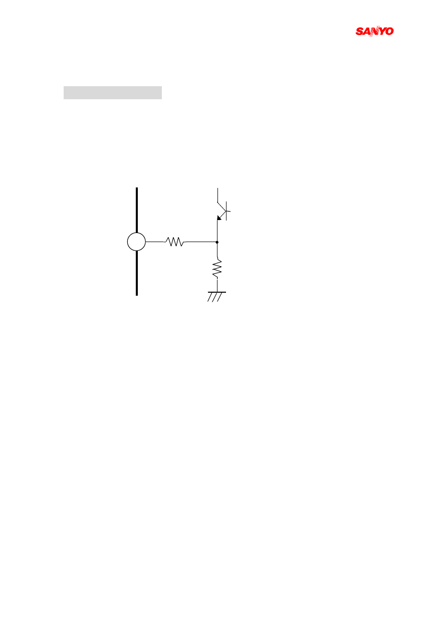
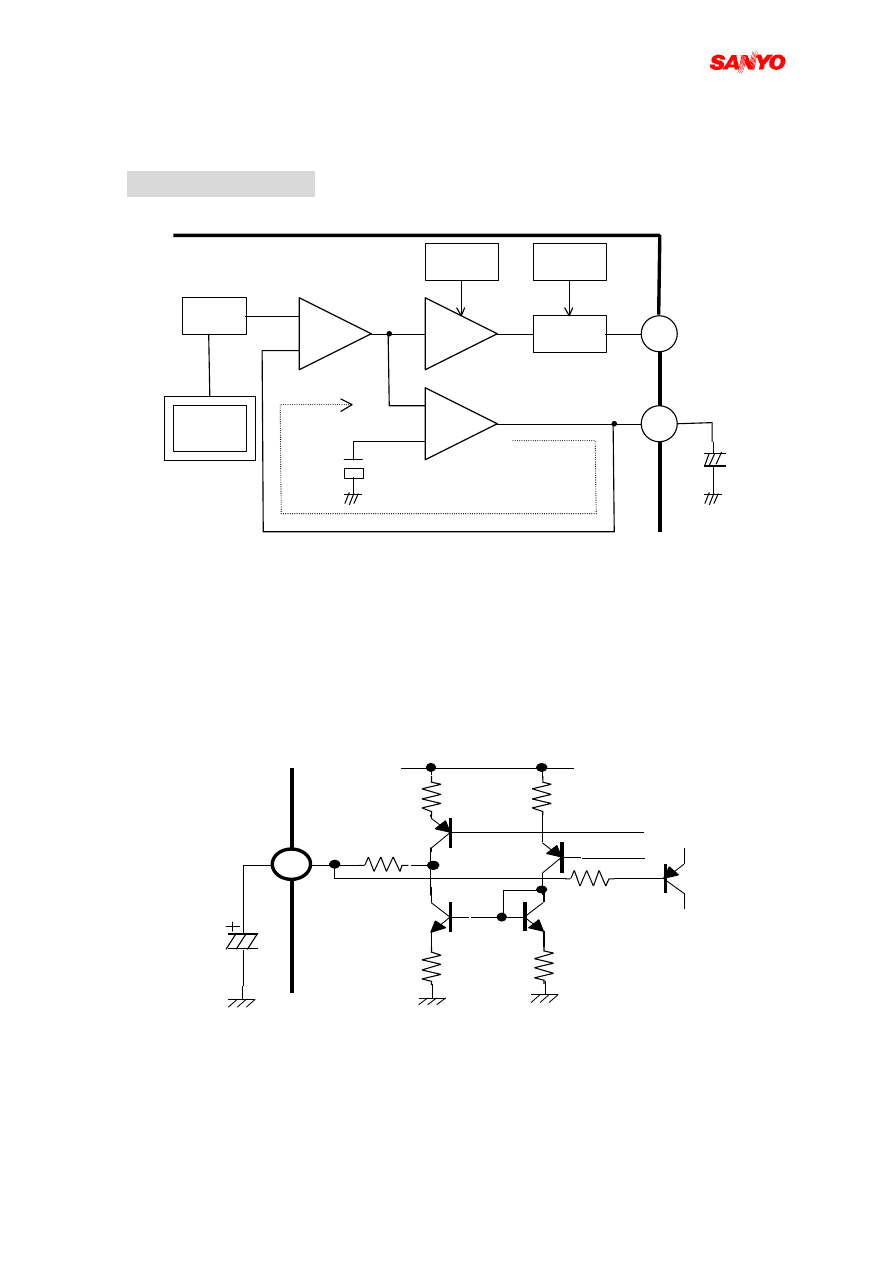
PIN 1 (Audio Output)
This is an audio output pin. The output impedance is about 300Ω and the DC output
is about 2.3V. The dynamic range of it is 3.5Vpp.
There is an attenuator between input (int.: pin 2; ext.: pin 51) and output, whose
maximum gain is 0dB and DAC step is 0.5dB. Also, a LPF (fc = 30Hz) is built-in
between D/A circuit and volume circuit to solve the ‘POP’ noise problem which is
caused by the volume control.
Circumference circuit of pin 1
150
1
10K
Technical Note of LA76818 2001/02/08
13/ 46
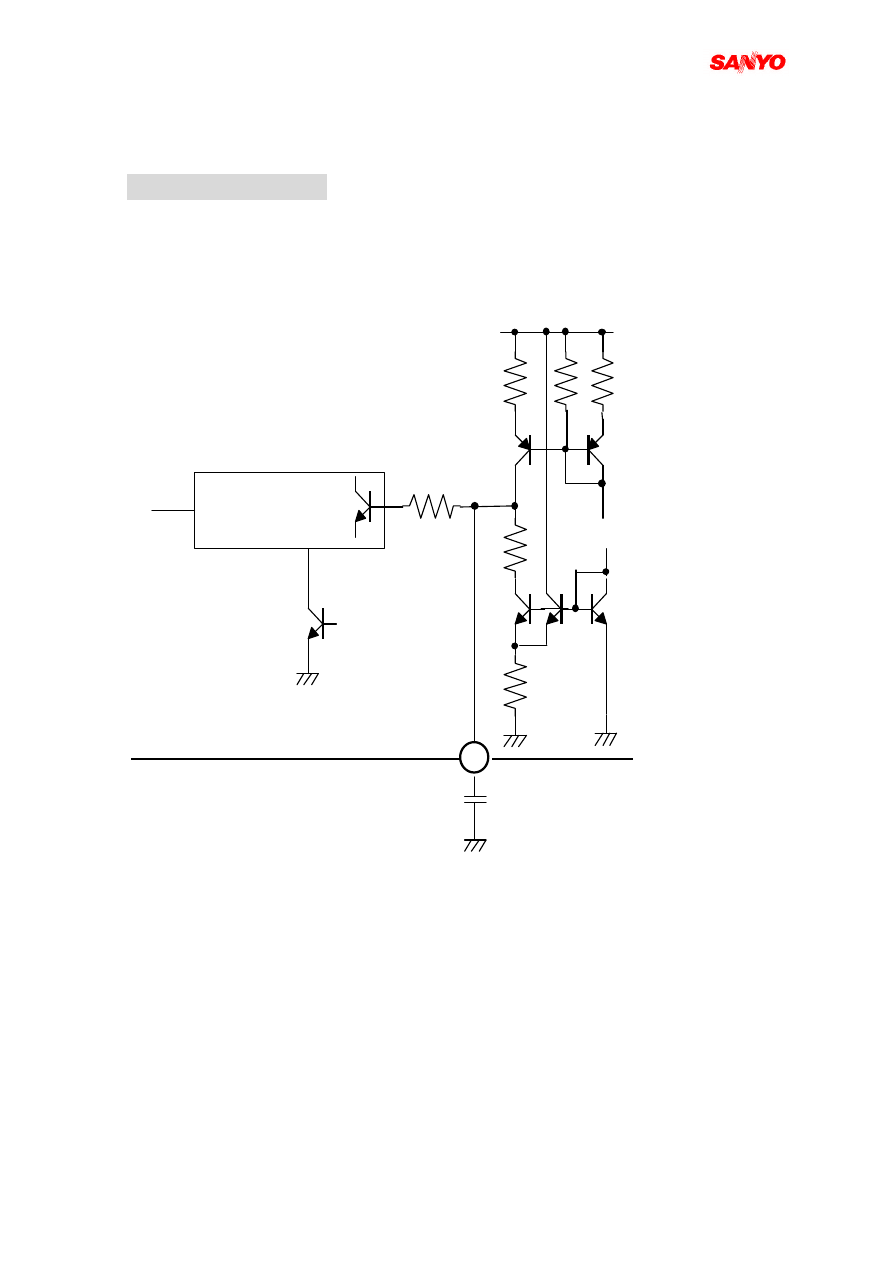
Pin 2 (FM Output)
This is an output pin for FM detector. The output circuit is a voltage follower.
The DC voltage is about
2.5
V and the dynamic range is
4
V.
The setting of BUS is depending on the frequency of SIF:
SIF frequency
BUS setting
4.5MHz
‘00’
5.5MHz
’01’
6.0MHz
‘10’
6.5MHz
‘11’
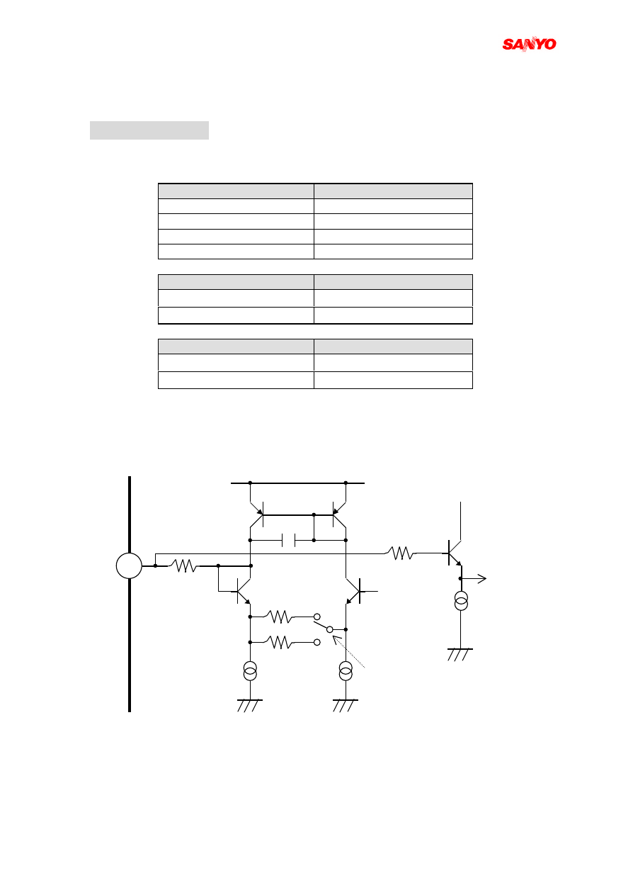
The output level is variable which is controlled by BUS:
BUS setting for FM Gain
Output level
‘0’
900mVrms (±50KHz)
‘1’
900mVrms (±25KHz)
The output impedance is variable which is controlled by BUS:
BUS setting for Deem-TC
Output Impedance
‘0’
5.0KΩ
‘1’
7.5KΩ
The time constant of the de-emphasis is determined by the value of external
capacity (0.01uF). There is no necessary to connect an external capacity if a stereo IC
is used. But, the output impedance is very high. This pin is also used to be an internal
pin for audio SW.
The circumference circuit of pin 2
2K
R1(PAL)
R2(NT)
300
2
FM 檢波信號
BUS:Deem
-TC
Audio
SW
300u
300u
50u
Technical Note of LA76818 2001/02/08
14/ 46
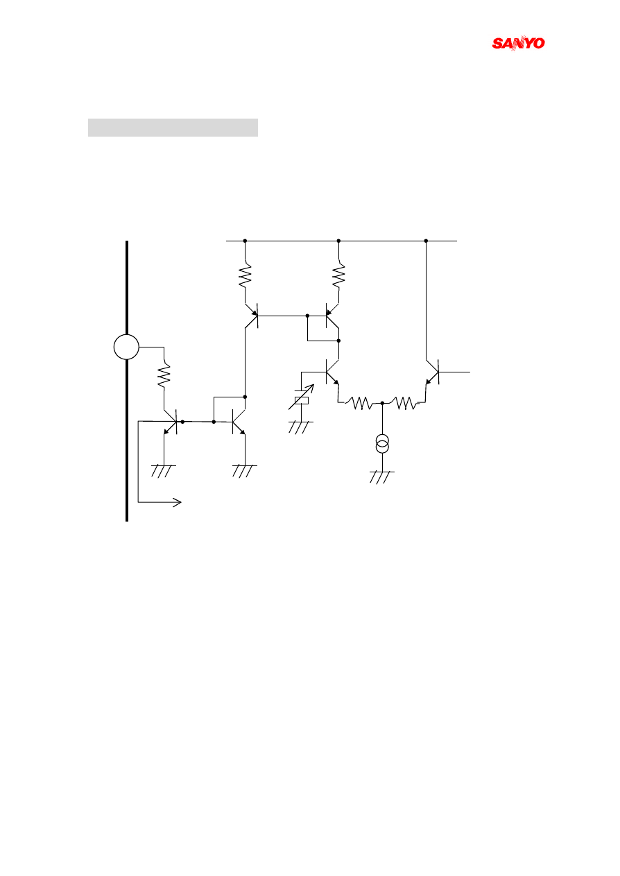
PIN 3 (IF AGC Filter)
This is 1
st
AGC filter pin. The signal, which is peak detected by the AGC
detector, is smoothed by the external capacitor and become to AGC voltage. The 2
nd
AGC filter is also built-in into IC. The value of C1 is depending on the speed of AGC,
sag etc, and the recommend value is about 0.022uF.
If the BUS of IF AGC is set as ‘1’, the gain of PIF is set minimally.
IF AGC
defeat
C1
Vcc
3
2nd
AGC Filter
The circumference circuit of pin 3
Technical Note of LA76818 2001/02/08
15/ 46
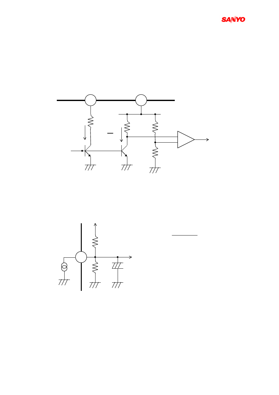
PIN 4 (RF AGC OUTPUT)
This is a RF AGC output pin. The reference voltage, which is controlled by RF AGC
D/A, and the IF AGC voltage is input into differential amplifier, then the output can be
achieved at the open collector. The time constant is determined by the value of the
external R & C. The maximum drive current of Q1 is 1mA. The maximum DC voltage
of pin 4 is
9
V. Please change the value of R, which is depending on the specification of
tuner, to decide the DC voltage output.
A) The circumference circuit of pin 4
4
2nd
IF.AGC
Filter
Output
RF
AGC
D/A
100
To BUS
Status
Technical Note of LA76818 2001/02/08
16/ 46
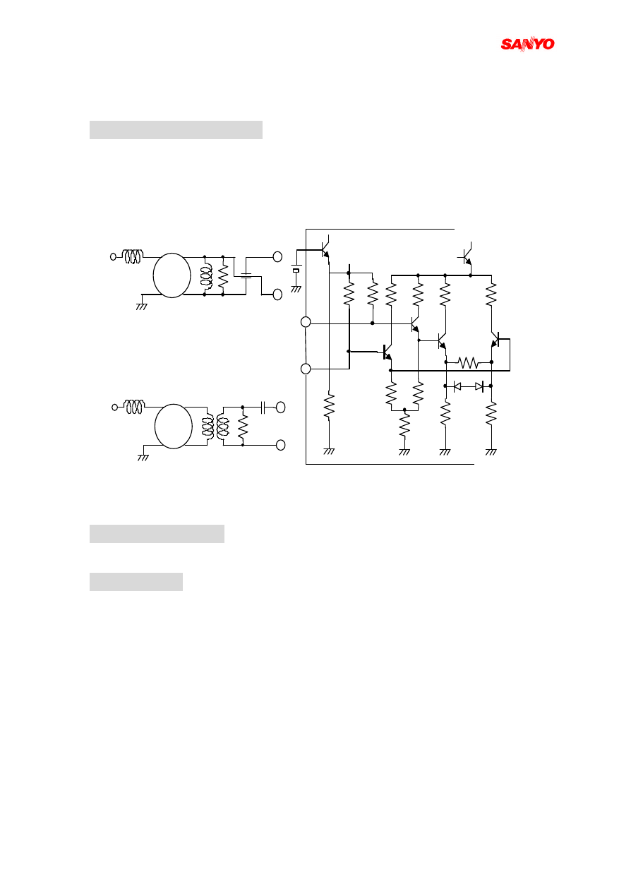
A comparator, which is used for BUS statue, is built-in this IC. The reference voltage
of this comparator is set as Vcc*(6/7) and compare with voltage below:
Vcc – {Io*(1/5)*70kΩ}
* Io is the output current of pin 4.
B)The circumference circuit of pin 4
[The example application circuit]
The BUS statue is ‘1’ if Vb, R1, R2 is set as below and the Vout is 6V:
Vb = 9V, R1 = 30KΩ, R2 = 120KΩ
R2
Vout (Vb-Io・ R1)
R1+R2
4
R1
R2
VB
Vout
+
Io
To
BUS
5
Io
1
+
−
Q2
4
Ra
8
70k
100
Rb
Q1
Io
RF.A
IF.VC
Io: max 1mA
Ra:Rb=1:6
Technical Note of LA76818 2001/02/08
17/ 46
PIN 5,6 (PIF AMP INPUT)
This is a PIF input pin. The input impedance Ri is about 1.5kΩ and the input
capacity is about 5pF.
This is a balanced input and it needs a 0.01uF capacitor for coupling. The balanced error
generated in the SAW filter and the printed plate can be canceled and the weak field
characteristic may be improved by using C1 to cross the IC input pin layout on the
printed plate.
SAW
tuner
From
SAW
tuner
From
1K
1K
3.6V
5
6
5
6
6
5
C1
C1
15K
The circumference circuit of pin 5 & 6
PIN 7 (IF GROUND)
This is the ground of IF circuit..
PIN 8 (IF Vcc)
This is DC voltage supply pin for IF circuit. Please add a 5.0Vdc to it.
Technical Note of LA76818 2001/02/08
18/ 46
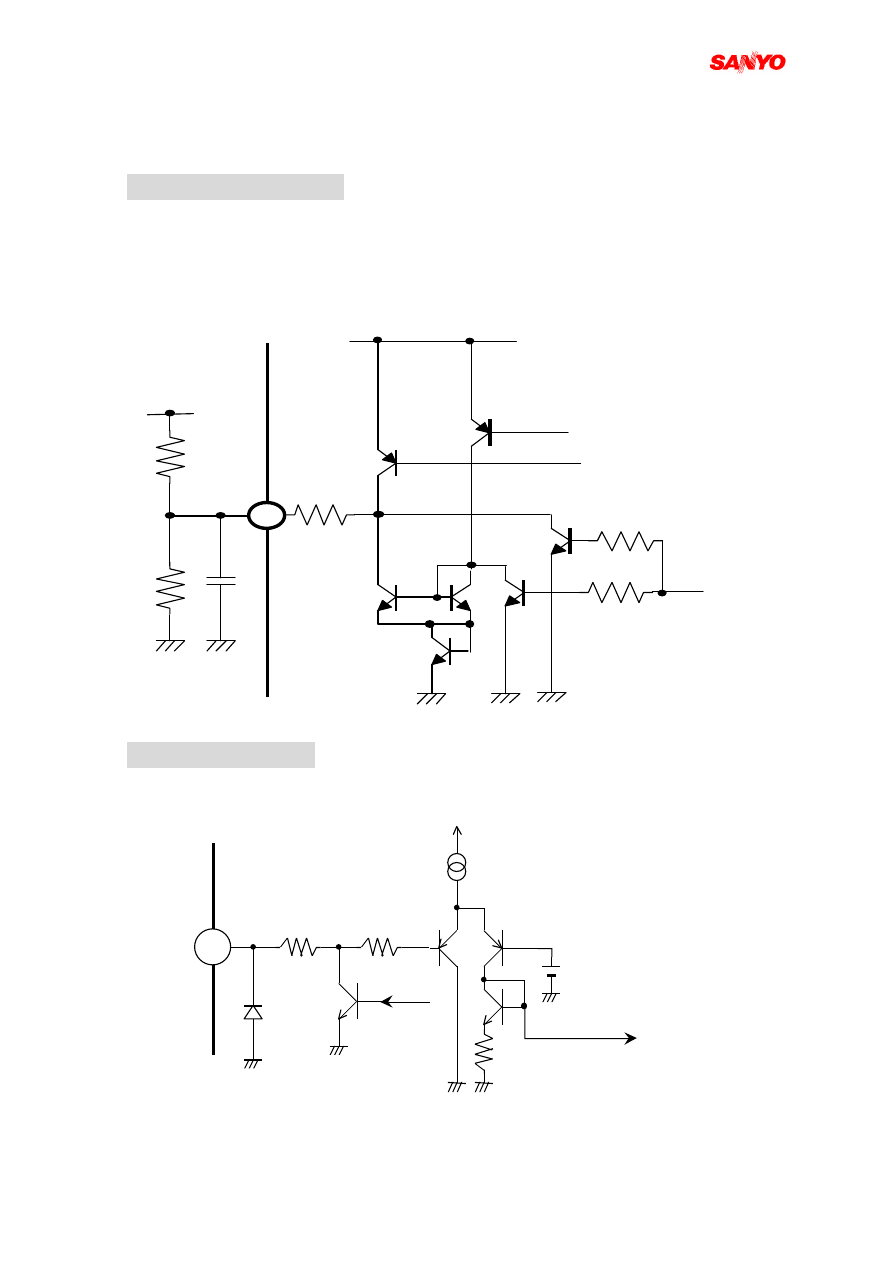
PIN 9 (FM FILTER)
This is the filter pin for the DC loop of FM detector.
Using PLL FM detection will cause DC shift during detecting SIF from
4.5MHz to 6.5MHz. But, this IC detects SIF signal from 4.5MHz to 6.5MHz at
good linearity range. Then it will pass through a amplifier after the DC output is
fixed. In order to keep the DC output constantly, feedback loop of the operating
amplifier is built-in into the IC. And it is also necessary to feedback a DC
component, which is created by the external capacitor of pin 9. The recommend
value of this capacitor is 1uF. The characteristic of low frequency and the respond
time when FM signal input is depending on the value of this capacitor. And it is
also possible to decrease the FM detection level by connecting a resister serially
with pin 9.
The circumference circuit of pin 9
1k
1u
1k
9
+
-
FM AMP
9
FM LEVEL
+
2
WRITE
5BIT
De-emph
+
-
FM DET
2.5
V
DC loop
Deem-TC
FM.Gain
Technical Note of LA76818 2001/02/08
19/ 46
PIN 10 (AFT OUTPUT)
This is an AFT output pin. The output is achieved from the collector of the current
mirror circuit. The control sensitivity of AFT can be adjusted by the external resister
(R1, R2). The current mirror circuit doesn’t operate at around center frequency (fo±
35KHz), and the voltage of pin 10 is determined by the external resister (R1, R2). The
control sensitivity of AFT is about
40
mV/kHz when R1 = R2 = 1MΩ.
The BUS control is fixed at “L” when IF PLL is unlocked.
1 M
1 k
R 2
1 M
F r o m
L o c k
D e t
R 1
1 0 0 0 p
1 0
The circumference circuit of pin 10
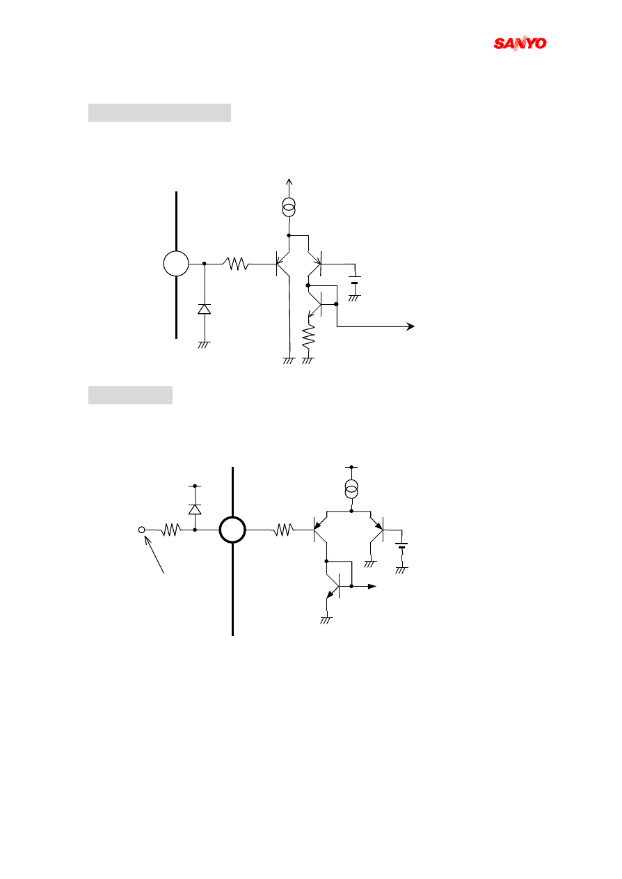
PIN 11 (BUS DATA)
This is a BUS Data input pin.
Vcc
600
11
50
1.8V
5k
ACK
Technical Note of LA76818 2001/02/08
20/ 46
PIN 12 (BUS CLOCK)
This is a Bus Clock input pin.
PIN 13(ABL)
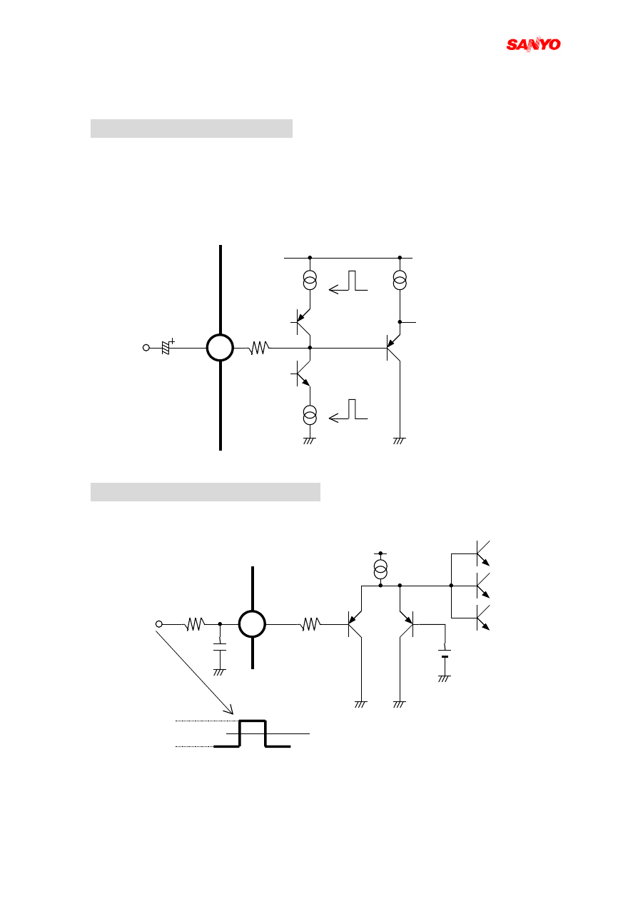
* ABL (Auto Beam Limiter) Function
This is a ABL / ACL input pin. Please transform beam current into voltage.
* Please refer data-sheet about the characteristics in detail.
470
Vcc 5.0V
100
100uA
Ref.Voltage
4.0 Vdc
IB(BEAM CURRENT)
VOLTAGE IN
13
Contrast ABL/BRT ABL
1.8V
600
12
Vcc
5k
Technical Note of LA76818 2001/02/08
21/ 46
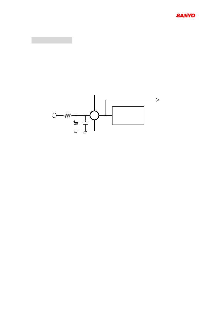
PIN 14, 15, 16 (R, G, B INPUT)
This is a OSD input pin. It can be used in either digital input mode or analog input mode.
A coupling capacity is necessary.
14 PIN : R INPUT, 15 PIN : G INPUT, 16 PIN : B INPUT
Input Signal:
u Analog Signal 0.7V (Black Level - White Level)
u Digital Signal High Level : 5V(Max)
Note: OSD signal is controlled by brightness and contrast. (OSD signal is impressed on
external video signal before brightness and contrast control).
PIN 17(FAST BLANKING INPUT)
This is a OSD fast blanking input pin. The threshold voltage is 1.4V.
1uF
100
200uA
CLAMP
CURRENT
200uA
CLAMP
CURRENT
200uA
BGP
BGP
Pedestal Clamp
R
100
200uA
Ref. Voltage
2.0Vdc
47pF
1.1k
Input Signal
1.4Vdc
Threshold
G
B
5.0V
0V
Technical Note of LA76818 2001/02/08
22/ 46
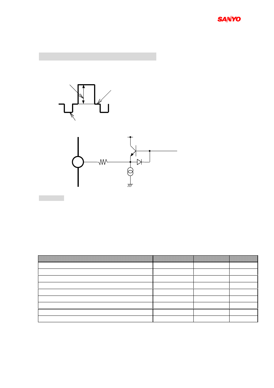
PIN 18(RGB Vcc)
This is a Vcc input pin of RGB output block. A 8.0V regulator is built-in in the IC and
please supply a current of 18mA to it.
A resister is needed to connect with this pin from Vcc. The value of the resister is
decide as below:
R[Ω] = (Vcc - 8.0)/18m
For example: Vcc = 9.0V, then a 8.2Ω resister is necessary.
R
Vcc
18
8V Regulator
Vcc R,G,B Out
10μ
10000p
Technical Note of LA76818 2001/02/08
23/ 46
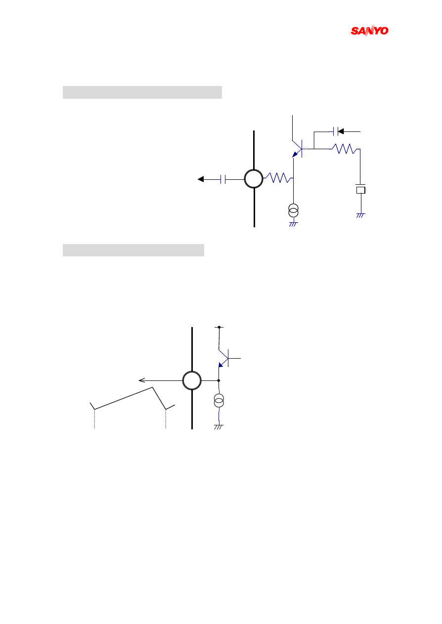
PIN 19, PIN 20, PIN 21(R, G, B OUTPUT)
This is a R, G, B signal output pin. ( 19 PIN : R OUT, 20 PIN : G OUT, 21 PIN : B
OUT )
Output Signal
Condition *1 :
•
Contrast Control
(7 bit)
: Max
•
Brightness Control
(7 bit)
: Mid ( 100000 )
•
Sub-Brightness Control
(7 bit)
: Mid
•
R, B Drive Control
(7 bit each )
: Max
•
G Drive Control
(4 bit )
: Min
•
R, G, B Bias (Cut-Off) Control
(8 bit each )
: Min
Each control variable range is show below:
Input signal:1Vpp (Sync Tip to White) = 140 IRE
Min
Typical
Max
Y Total Gain (Max)
10 dB
12 dB
14 dB
Contrast Control Max/Mid
4 dB
6 dB
8 dB
Contrast Control Range Min/Max (128-step)
-15 dB
-12 dB
-9 dB
Brightness Control Max/Mid (64-step)
15 IRE
20 IRE
25 IRE
Brightness Control Min/Mid (64-step)
-25 IRE
-20 IRE
-15 IRE
Sub-Bias Control Range (128-step)
700 mV
800 mV
900 mV
Bias Control Range (256-step)
700 mV
800 mV
900 mV
G Drive Reduction Control Range (16-steps)
R,B Drive Reduction Control Range(128-step)
7 dB
9 dB
11 dB
RGB Output Level : 3.0Vpp
Pedestal Level : 2.1VDC
(Temperature Characteristic.:‑2mV/℃)
Blanking Level : 1.5VDC @ Condition *1
100
1mA
R, G or B
Pedestal Level
0 IRE Level
R,G,B
Output
Level
Blanking
Level
Technical Note of LA76818 2001/02/08
24/ 46
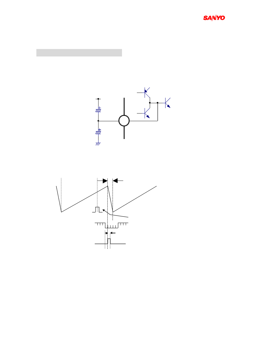
PIN 22(fsc output or c-sync. output)
The output of this pin can be selected by BUS be either fsc output or c-sync output.
If 4.43MHz output is needed, the application is used as below:
PIN 23 (VERTICAL OUTPUT)
This is a output pin of vertical synchronization ramp signal. We recommend using
together with LA7840 serial. Below are some functions which can be control by BUS:
V.DC
: position of field
(6 bit)
V. size
: size of field
(7 bit)
V. linearity
: linearity
(5 bit)
V. SC
: S compensation
(5 bit)
The application of vertical position adjustment circuit is different depending on either
using ± dual voltage supply or single voltage supply. Please refer to technical note
of LA7840/LA78040 (Vertical output IC).
300μA
23
Vcc
to LA7840
1 Field
22
3.25V
20k
15p
1k
0.01u
80uA
CW
CW
Technical Note of LA76818 2001/02/08
25/ 46
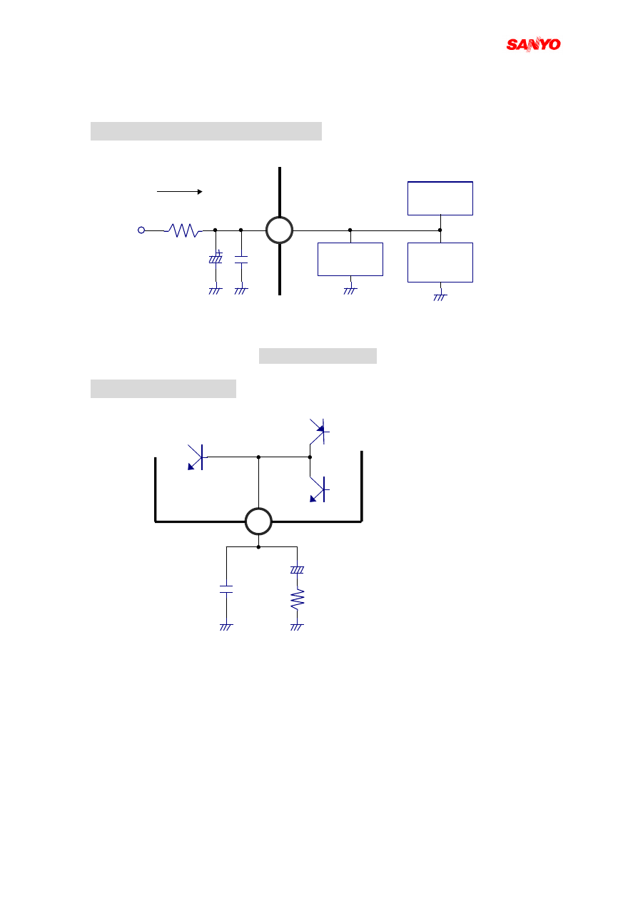
PIN 24 (V RAMP ALC FILTER)
For achieving more stable ramp output, the slope of the ramp output is fixed by adding
an ALC (automatic level control) loop to the ramp generator, which is the reference of
the vertical output. A smoothing capacitor, which is part of the loop, is connected to pin
24.
Note)
Normally, the voltage of pin 24 is controlled at around 2.5V. The time constants of the
ALC become very long due to only sampling 1 H during V period. It is possible that it
unable to catch up the rapidly temperature change, so please be careful in your design.
Besides, because of the hold period of sampling is very long, don’t let a leakage current
flow into pin 24.
ALC is proceeded at the position which is either 224.5H (NTSC)or 268H (PAL) apart
from the internal reset timing. The slope is controlled constantly, if a non-standard
signal (1 field = 262.5H or 312.5H) is input, the size of the screen will change. The pull-
in range of the count-down system is 226〜296 in NTSC system, or 288H〜357H in
PAL system.
Ramp Retrace
ALC pulse
224.5H (NTSC)
Count by the internal count-down circuit
0.5H
0
Vertical Sync. Signal
The reset timing of
the internal count-
down system.
0.33μ
24
0.33μ
Vcc
C1
C2
Technical Note of LA76818 2001/02/08
26/ 46
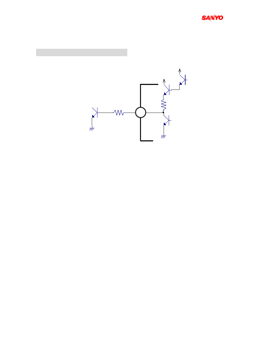
PIN 25 (HORIZONTAL / BUS Vcc)
This is a Vcc pin of horizontal deflection block and BUS interface block.
Choose the value of the resister R1 to let the current flow into pin 25 is 26mA.
The value of the resister is decide as below:
R1 = (+B-5.0V)/27mA
PIN 26(AFC FILTER)
This is a AFC filter pin of horizontal VCO.
C1 is used for canceling the vertical ripple, while the resister R1 is used for
transforming the control current into voltage. C2 is a smoothing capacitor.
Reference value
:
C1 = 1.0μF
C2 = 0.015μF
R1 = 3.0KΩ
26
C1
R1
C2
Shunt
Reg.
Hor OSC
AFC
H.DRIVE
25
R1
Icc=27mA
+B
BUS
I
n
t
e
r
f
a
c
e
Technical Note of LA76818 2001/02/08
27/ 46
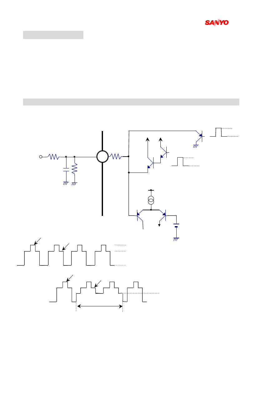
PIN 27 (HORIZONTAL OUTPUT)
This is a horizontal output pin, and its output circuit is push-pull circuit.
The maximum collector current of the Tr. 1 is 3mA. Usually, R1, which is used for
reducing the influence of horizontal output to IF block, is recommended to be set at 100
Ω. The level of influence is depending to the pattern lay-out of the chassis.
Note) The duty of the horizontal output pulse is designed at 37.6μs in low period.
27
Hori Output
R1
Tr1
1.8K
Technical Note of LA76818 2001/02/08
28/ 46
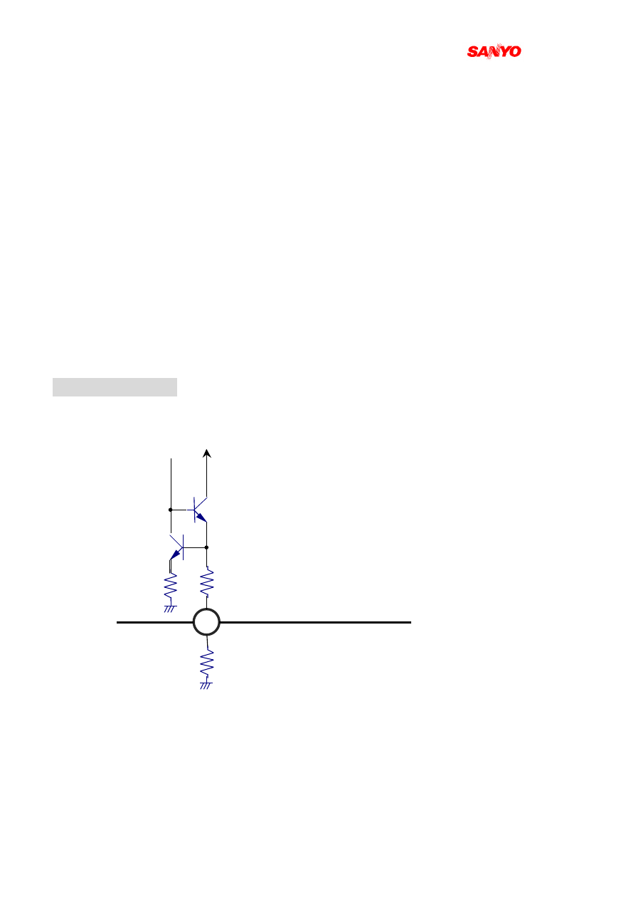
PIN 28 (FBP INPUT)
This is the input pin of flyback pulse, which is used for AFCⅡ. The threshold voltage at which
the flyback pulses are acquired internally by the IC is 3/5*Vcc. (For example, if the Vcc is 5V, it
is 3V). The fly-back pulse is input via R1 and R2. Besides, although the input flyback pulses are
input to the AFCⅡloop to take up the horizontal output storage time, since the screen center is
offset in advance, the flyback pulses must be matched to the screen center by adjusting the
integration provided by R1 and C1. This IC has a function which is used for horizontal position
fine adjustment:
Horizontal Phase
: the horizontal center of the screen can be adjusted by bus-controlled. (5bit)
Besides, if the peak of input FBP of pin 28 is exceeding 4V, BGP and vertical output for
LA7642N (SECAM decoder) can be achieved.
5.0V
3.3V
BGP
FBP
5.6V
4.0V
0.4V
Standard Hori. Trace period
FBP
R1
R2
C1
28
2ndAFC
3/5*Vcc
BGP
Vcc
Vcc
1.4V
SECAM V
3.4V
300
BGP
FBP
2.0V
Vertical retrace time image
SECAM V 期間
Technical Note of LA76818 2001/02/08
29/ 46
Note1)
The best storage time of this IC, between the rise up of Horizontal output (pin 27) and the rise up
of input FBP, is about 9μs. Therefore, the storage time of television chassis is better set at 9μs
±2s.
Note 2
In LA76810 serial, FBP is not used in the blanking of RGB output. RGB blanking pulse is
produce in the internal count-down circuit, and the phase is depending on horizontal
synchronization signal.
Concerning to the phase and the width of blanking pulse, as before waveform is made up and
designed suitably in FBP input circuit. But, in LA76810 serial, the phase and the width of
blanking pulses (H BLK R&L) can be set by BUS control. Therefore, the design of FBP input
circuit (adjustment of horizontal phase, jitter characteristic etc) become more easier. Also, in
case of develop many chassis, this can contribute to speed up the development period.
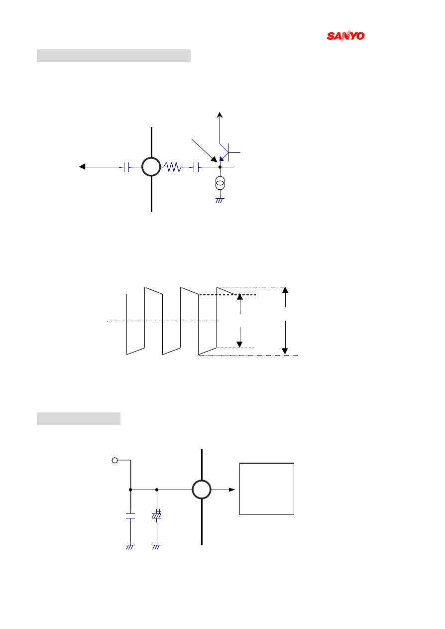
PIN29 (I reference)
This is a pin for producing reference current. Use a resister of 4.7K to connect with ground from
this pin.
Note)
During the stage of evaluation of this IC (engineering sample), bus-control is used to adjust the
horizontal frequency (H freq. = 6 bit). But no more adjustment of horizontal frequency is needed
in the mass-production products. Depending on the accurate level of horizontal free-run
frequency we need, a low offset external resister is requested.
29
70
2.6k
4.7k
Technical Note of LA76818 2001/02/08
30/ 46
PIN 30(4MHz CLOCK OUTPUT)
This is an output pin of a 4MHz ( accurately is 256*fh Hz) clock.
Please use a 10000p coupling capacitor for output to LA7642N. If LA7642N is not using, please
open this pin.
We can get a amplitude of 2/3Vcc±1Vbe at point A.
The waveform of pin 30 is shown below:
The duty of this waveform is 50%.
PIN 31( CCD Vcc)
This is a Vcc (5V) pin for 1 H delay-line.
±0.8Vpp
±0.65Vpp
2/3Vcc
Vcc
1k
30p
30
To SECAM Decoder IC
LA7642N
10000p
A
200μA
Vcc
FROM 4MHz VCO
31
1HDL
VCC:(5V)
1H
Delay Line
4.7μ
0.01μ

Technical Note of LA76818 2001/02/08
31/ 46
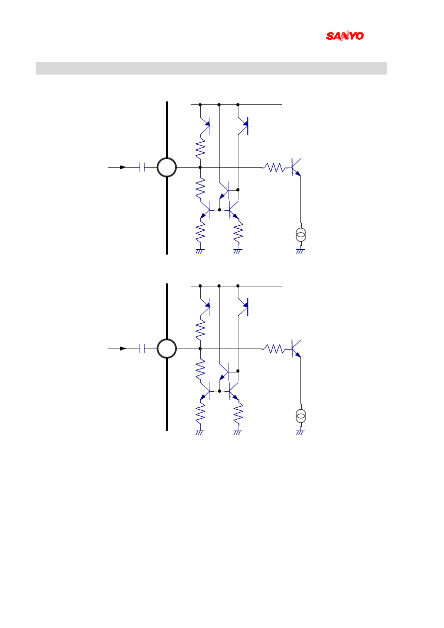
PIN 32( CCD FILTER)
This is the filter pin of the built-in 1H delay-line circuit.
PIN 33(CCD & DEFLECTION GDN)
This is the ground pin of CCD & deflection block.
32
Booster
1μ
Technical Note of LA76818 2001/02/08
32/ 46
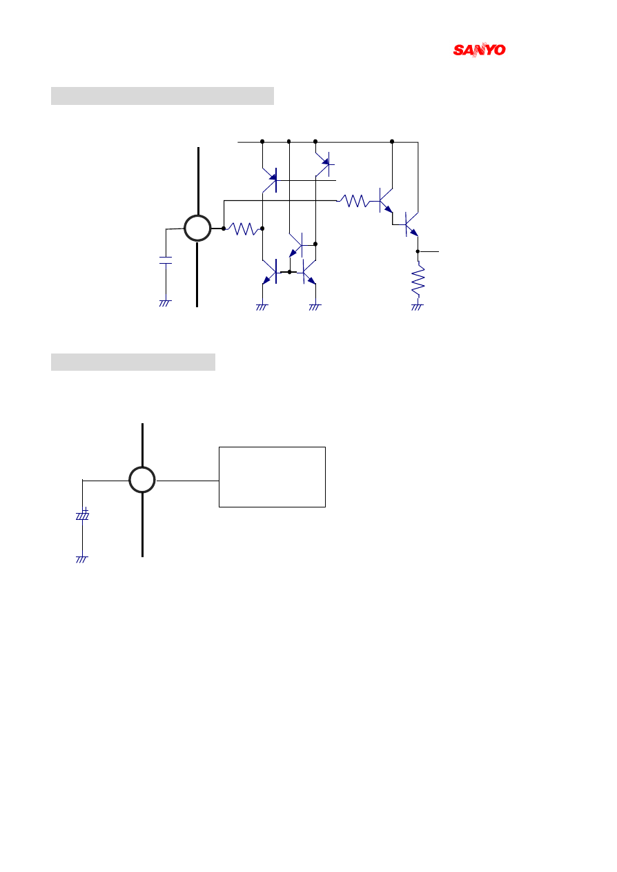
34, 35 PIN (SECAM INPUT or CbCr INPUT)
This is a SECAM signal input pin, and CbCr input pin. Select Bus DATA.
34
1K
1K
2K
2K
1K
0.1μ
LA7642N
35
1K
1K
2K
2K
1K
50μA
50μA
R−Y
0.1μ
LA7642N
B−Y
Technical Note of LA76818 2001/02/08
33/ 46
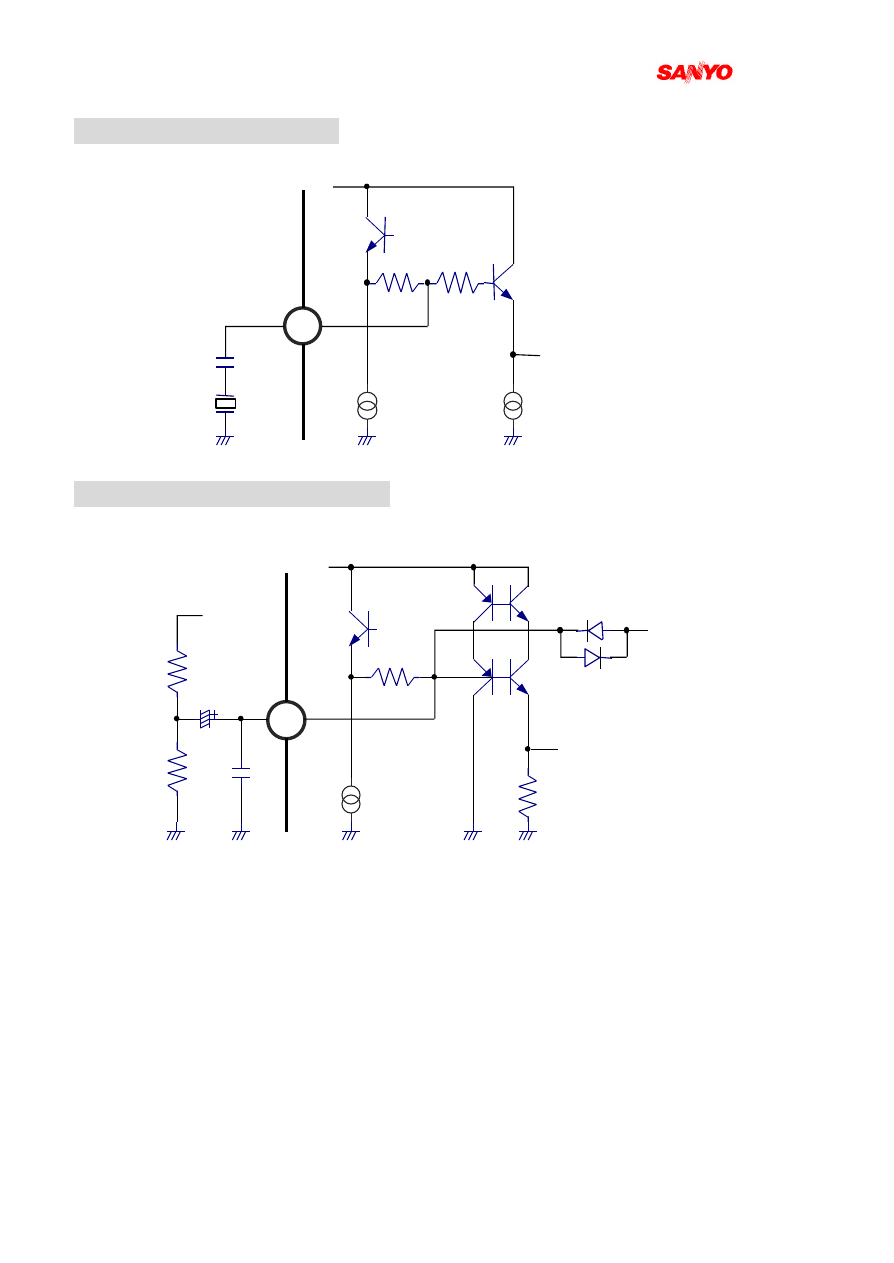
PIN 36 (CHROMA APC2 FILTER)
This is filter pin for AFC filter of chrome VCO.
PIN 37(CLAMP FILTER)
This is a filter pin for Y signal clamp circuit bias filter.
10K
VCO
CONTROL
AFC DET
OUT
100
200
36
100p
37
10μ
Y Clamp
Bias
Technical Note of LA76818 2001/02/08
34/ 46
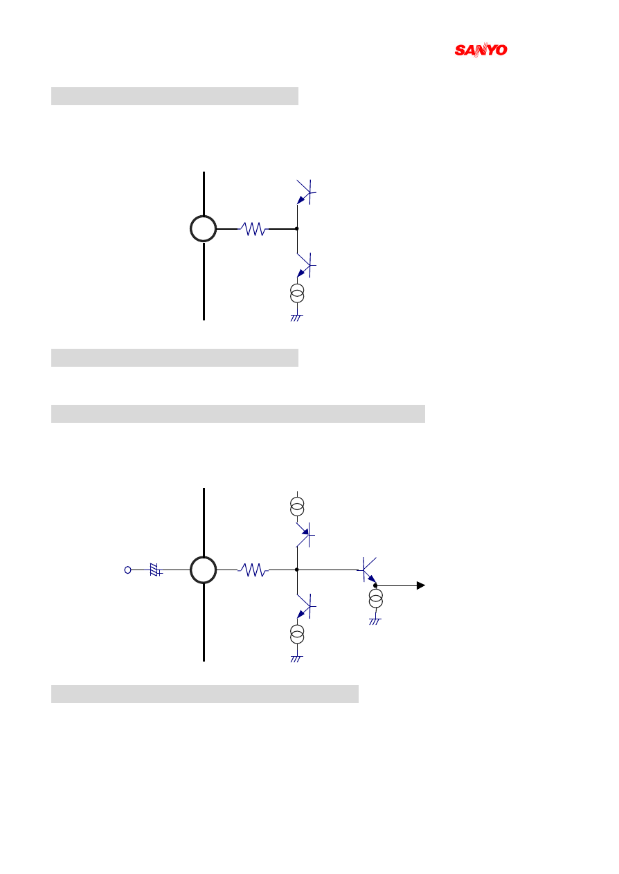
PIN 38(4.43MHz CRYSTAL)
This is a 4.43MHz x’tal connecting pin.
PIN 39(CHROME APC1 FILTER)
This is a filter pin for APC filter of chrome VCO.
39
3.9K
39K
300μA
(BGP:ON)
APC DET
OUT
VCO
CONTROL
Vcc
24K
24K
0.47μ
0.01μ
38
620
100μA
600
200μA
CW:
TINT
CW SW
4.43
Technical Note of LA76818 2001/02/08
35/ 46
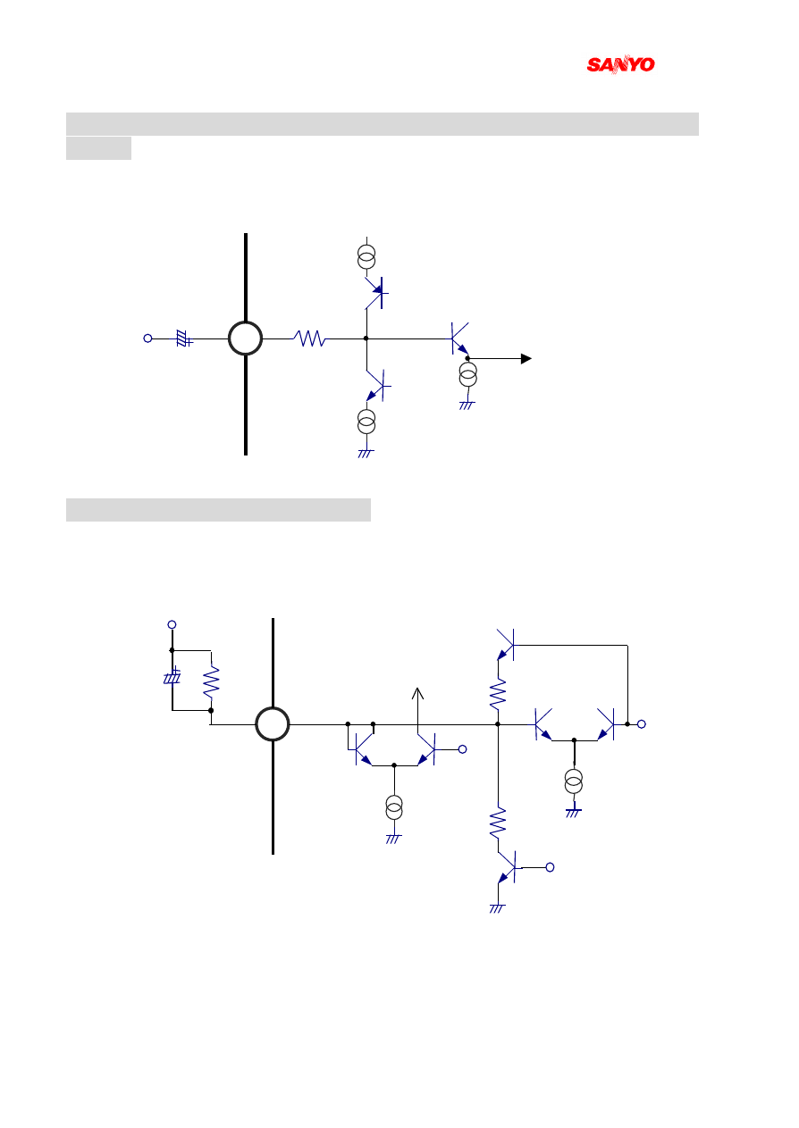
PIN 40(SELECTED VIDEO OUTPUT)
This is a output pin of selected video signal. This signal, which is selected by a video switch
among 42 pin or 44 pin input signal, is amplified 6dB and then output here. The output
amplitude is 2Vp-p.
PIN 41(Video Chrome Deflection GND)
This is the ground pin of video/ chrome/ deflection block.
PIN 42(EXT VIDEO INPUT & Y INPUT in S-VHS MODE)
This is an external video input pin. The pedestrian level of input signal is clamped at 1/2 Vcc by
charging & discharging external capacitor. Besides, this pin becomes input pin of Y signal in S-
VHS mode.
PIN 43(VIDEO CHROME DEFLECTION VCC)
This is a Vcc pin of video/ chrome/ deflection block.
40
100
1mA
42
1k
9uA
60uA
To Video SW
1uF
Technical Note of LA76818 2001/02/08
36/ 46
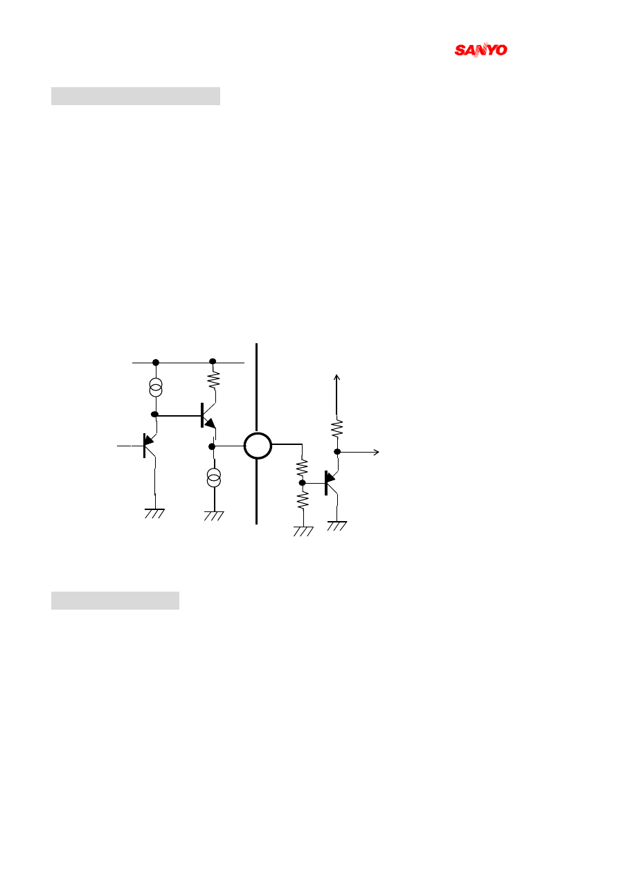
PIN 44(INT. VIDEO INPUT & CHROME SIGNAL INPUT IN S-VHS
MODE)
This is an internal video input pin. The pedestal level of input signal is clamped at 1/2 Vcc by
charging & discharging external capacity. Besides, this pin become input pin of chrome signal in
S-VHS mode.
PIN 45(BLACK STRETCH FILTER)
This is a filter pin for black peak level detection in black stretch circuit. The capacitor is charging
during black peak period, and discharging via external CR exclude black peak period. The DC
level of the output and the gain of black stretch will be reduced if the value of time constant is
large.
45
40uA
Defeat
1uF
680k
VCC
VCC
50uA
1/2VC
Y 信号
50k
1k
44
1k
9uA
60uA
To Video SW
1uF
Technical Note of LA76818 2001/02/08
37/ 46
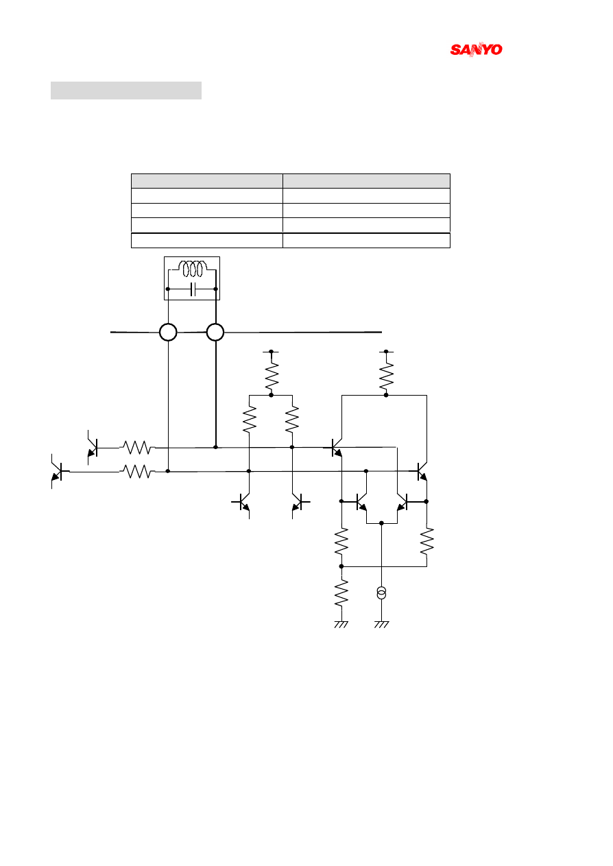
PIN 46 (VIDEO OUTPUT)
This is a video output pin. The output is a low impedance circuit.
•
The video DC output is 3.5V when there is no signal.
•
Sync Tip Voltage is 1.2V
•
The video amplitude is 2.0Vpp
In addition, there is a Black Noise Inverter Circuit built-in in this IC.
•
The threshold voltage of Black Noise Inverter is
0.8
V
•
The replacement voltage of Black Noise Inverter is
1.9
V
The built-in sound trap is linked with the BUS (SIF SYSTEM) that the trap frequency is set
automatically depending on the SIF frequency. In order to prevent the unsatisfied drive capacity
of amplitude matching (1Vpp) and load (video circuit, chroma circuit, deflection circuit), we
recommend application circuit below:
The circumference circuit of pin 46
PIN 47 (VCO Filter)
This is a VCO filter pin. The phase of the signals, which are divided from chroma frequency
and VCO frequency, will be compared together. Then the discrepancy phase will transform to be
current and output to pin 50. This current will smoothed at the external capacitor and the free-run
frequency of IF VCO is controlled at center. If the value of external capacitor is large enough, it
can prevent the unstable of free-run frequency from floating input frequency or external noise.
But the time constant becomes longer at the same time when power on. Therefore, the
recommend value of this capacitor is 0.1uF.
Vcc
46
500u
Video Circuit
Chroma Circuit
Deflection Circuit
Technical Note of LA76818 2001/02/08
38/ 46
PIN 48, 49 (VCO COIL)
This are L & C connecting pin for IF PLL VCO. This is a vector synthesis VCO. An
exclusive VCO coil can be used according to the IF frequency. The BUS setting is depending on
the detection VIF frequency which shown below:
VIF Frequency
BUS setting
38.0MHz
‘00’
38.9MHz
‘01’
45.75MHz
‘10’
39.5MHz
‘11’
V c c
V c c
1 k
1 k
5 0 0
3 0 0
3 0 0
48
49
The circumference circuit of pin 48 & 49
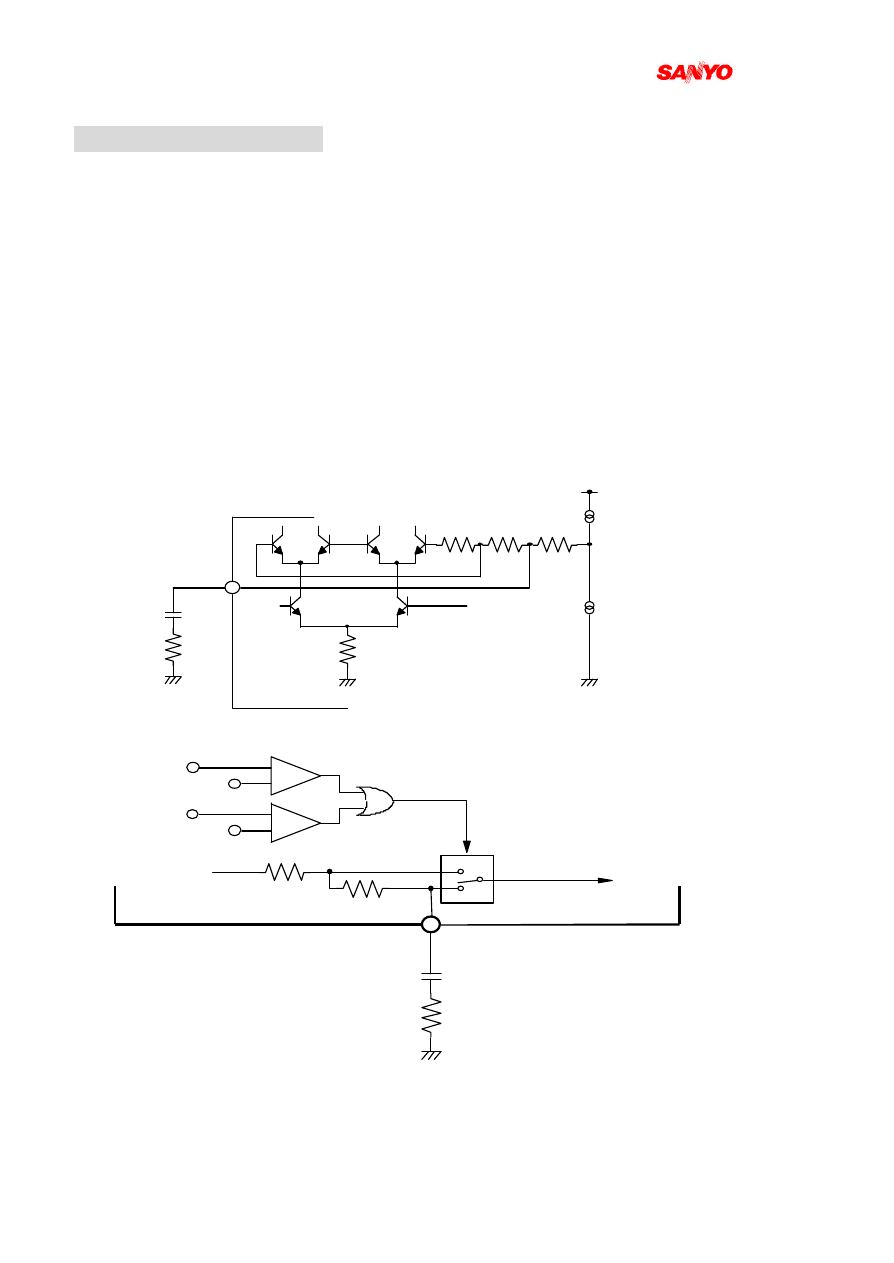
Technical Note of LA76818 2001/02/08
39/ 46
PIN 50 (PIF APC FILTER)
This is a APC filter pin for PLL circuit. It is connected with a APC switch, and the time
constant can be switched by lock detection circuit. First, the APC loop gain is determined by the
time constant (R1 & C1). If R1 is increased, the loop gain will increase and the pull-in range will
increase as well. But, the characteristic of the noise sensitivity will degrade at the same time,
therefore our recommended value for R1 is 150
Ω
. In the other hand, the time constant of APC
loop is determined by the capacitor C1 and the internal resistor inside IC. Therefore, if the
capacitor C1 is variable, the time constant of loop will change largely by every step. We
recommended the value of C1 is 0.47uF.
In addition, the lock detector circuit operate according to an OR gate whose input are IF AGC
voltage and the video signal. At the comparator, the PLL unlocked state of weak signal is
detected from IF AGC voltage and the PLL unlocked state when detuned is detected from the
video signal. Then the APC switch is switched to B position to expand the pull-in range.
V c c
F r o m L o c k D e t e c t o r
C 1
R 1
0 . 4 7 u F
1 5 0
3 0 0
5 6 0
1 k
4 8
(a) The circumference circuit of pin 47
C 1
R 1
1 5 0
‑
+
I F A G C
V 1
V i d e o
V 2
O u t p u t
‑
+
O R
1 k
5 6 0
B
t o V C O
A P C S W
A
0 . 4 7
u F
4 8
(b) The circumference circuit of pin 47
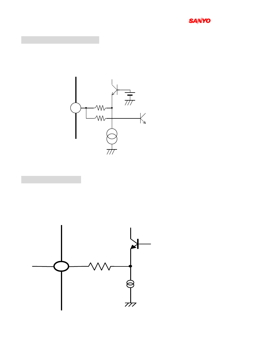
Technical Note of LA76818 2001/02/08
40/ 46
PIN 51 (EXT AUDIO INPUT)
This is an external audio signal input. The input impedance is about 50k and the DC
voltage is biased at about 2.9V. There is necessary to use a coupling capacitor to combine with it.
The circumference circuit of pin 51
PIN 52 (SIF OUTPUT)
This is a SIF output pin. The output of this pin is used when a NICAM IC is used. The
output of this pin is a follow-emitter, so its output impedance is about 350
Ω
. And the DC output
of this pin is about 2.8V.
If a signal, whose P/S is 25bB, is input into IC, a
96
dBu Snd will be outputted.
3 0 0
4 0 0 u A
5 2
The circumference circuit of pin 52
3.6V
50K
300
51
50u
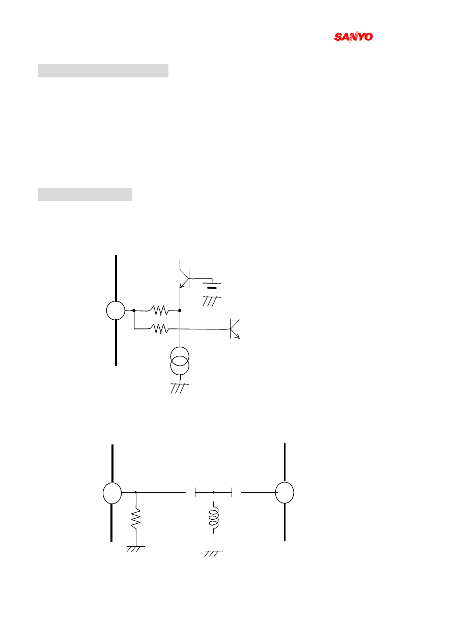
Technical Note of LA76818 2001/02/08
41/ 46
PIN 53 (SND APC FILTER)
This is a SND APC FILTER pin. The phase of the signals, which are divided from
chroma frequency and Snd-VCO frequency, will be compared together. Then the discrepancy
phase will transform to be current and output to pin 53. This current will smoothed at the
external capacitor of pin 53 and control Snd-VCO.
BUS: The dividing ratio of Snd-VCO, which is depending on the SIF system, is variable. The
oscillator frequency of Snd-VCO is locked at the frequency which is 500k apart from SIF
frequency.
PIN 54 (SIF INPUT)
This is a SIF input pin. The input impedance is about 1kΩ and the internal DC voltage is
biased at about 3.3V. The maximum input for this pin is
96
dBu. To improve the buzz
characteristic, we recommend the application circuit as below:
The circumference circuit of pin 54
Recommended application circuit
4.0V
1K
500
54
200u
52
54
15μ
47p
47p
1k
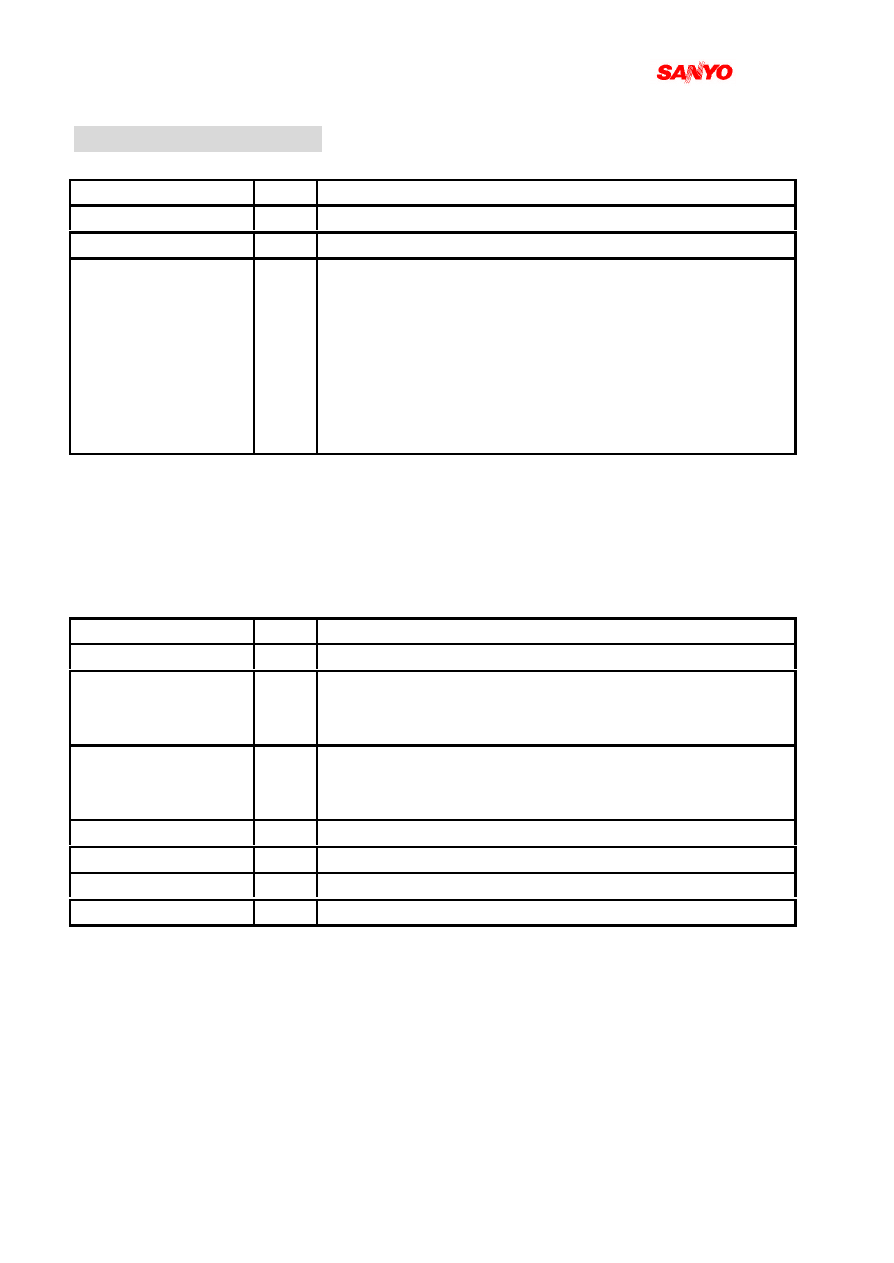
Technical Note of LA76818 2001/02/08
42/ 46
Statue Register of LA76818
Register Name
Bits
General Description
H Lock
1
H LOCK Detection
Killer
1
Color Killer operation output
Color System
3
000: B/W
001: PAL
010: PAL-M
011: PAL-N
100: NTSC
101: 4.43NTSC
110: SECAM
111: Do not care
Output the color system of IC which is operating.
If CPU set the Color System as Auto Mode, there is an output to indicate the color
system which is operating in the IC. The output will be ‘000’ if any mistake taken.
If CPU set the Color System as Manual Mode, specified mode is output. If
selection cannot be made, output ‘000’.
X Ray
1
X Ray Protection Detection
POR
1
Power On Reset
IF Ident
1
Detect sync signal of IF video detection output and
output the information. (corresponding to PAL 21
PIN connector)
RF AGC
1
Detect the output voltage of RF AGC, then compare it
with the reference voltage and output the information:
‘High’ or ‘Low’
IF.LOCK
1
Output the information (locked / unlocked) of PLL
V TRI
1
Detect vertical sync signal
50/60
1
Detect 50/60Hz mode
ST/NONST
1
Discriminate Standard / Enforced Non-Standard mode

Technical Note of LA76818 2001/02/08
43/ 46
LA76818 Pin Assignment
Pin
Function
Pin
Function
1
Audio Output
54
SIF Input
2
FM Output/Selected Audio Output
53
SIF APC Filter
3
PIF AGC
52
SIF Output
4
RF AGC Output
51
Ext. Audio Input
5
PIF Input1
50
APC Filter
6
PIF Input2
49
VCO Coil 1
7
IF Ground
48
VCO Coil 2
8
IF Vcc
47
VCO Filter
9
FM Filter
46
Video Output
10
AFT Output
45
Black Level Detector
11
Bus Data
44
Internal Video Input (S-C IN)
12
Bus Clock
43
Video/Vertical Vcc
13
ABL
42
External Video Input (Y In)
14
Red Input
41
Video/Vertical Bus Ground
15
Green Input
40
Selected Video Output
16
Blue Input
39
Chroma APC1 Filter
17
Fast Blanking Input
38
4.43MHz Crystal
18
RGB Vcc
37
Clamp Filter
19
Red Output
36
Chroma APC2 Filter
20
Green Output
35
SECAM R-Y Input(Cr input)
21
Blue Output
34
SECAM B-Y input(Cb input)
22
Fsc output/C-Sync output
33
CCD/Horizontal Ground
23
Vertical Output
32
CCD Filter
24
Ramp ALC Filter
31
CCD Vcc
25
Horizontal/Bus Vcc
30
Clock (4MHz) Output
26
Horizontal/AFC Filter
29
VCO IREF
27
Horizontal Output
28
Flyback Pulse Input
Technical Note of LA76818 2001/02/08
44/ 46
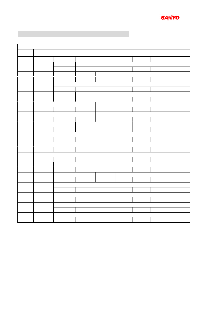
LA76818 Bus Control Resistor Bit Allocation Map
IC Address (Write): 10111010
Control Register Bit Allocations
Sub
Address
MSB
DATA BITS
LSB
DA0
DA1
DA2
DA3
DA4
DA5
DA6
DA7
00000000
T_Disable
AFC gain&gate
H.FREQ
1
0
1
1
1
1
1
1
00001 Vreset Timing
Audio.Mute
Video.Mute
H.PAHSE
0
0
0
1
0
0
0
0
00010
Sync.Kill
V.SIZE
0
1
0
0
0
0
0
0
00011
VSEPUP
V.KILL
V.POSI
0
0
1
0
0
0
0
0
00100 H BLK L
V.LIN
1
0
0
1
0
0
0
0
00101 H BLK R
V.SC
1
0
0
0
0
0
0
0
00110 V.TEST
V.COMP
COUNT.DOWN.MODE
0
0
1
1
1
0
0
0
00111 R.BIAS
0
0
0
0
0
0
0
0
01000 G.BIAS
0
0
0
0
0
0
0
0
01001 B.BIAS
0
0
0
0
0
0
0
0
01010
*
R.DRIVE
(0)
1
1
1
1
1
1
1
01011
Drive.Test
Half tone
Half tone Def G.DRIVE
0
0
1
1
1
0
0
0
01100
*
B.DRIVE
(0)
1
1
1
1
1
1
1
01101
Blank.Def
Sub.Bias
0
1
0
0
0
0
0
0
01110
IF Test1
Bright
0
1
0
0
0
0
0
0
01111
IF Test2
Contrast
0
1
0
0
0
0
0
0
(Bits are transmitted in this order.)
Technical Note of LA76818 2001/02/08
45/ 46
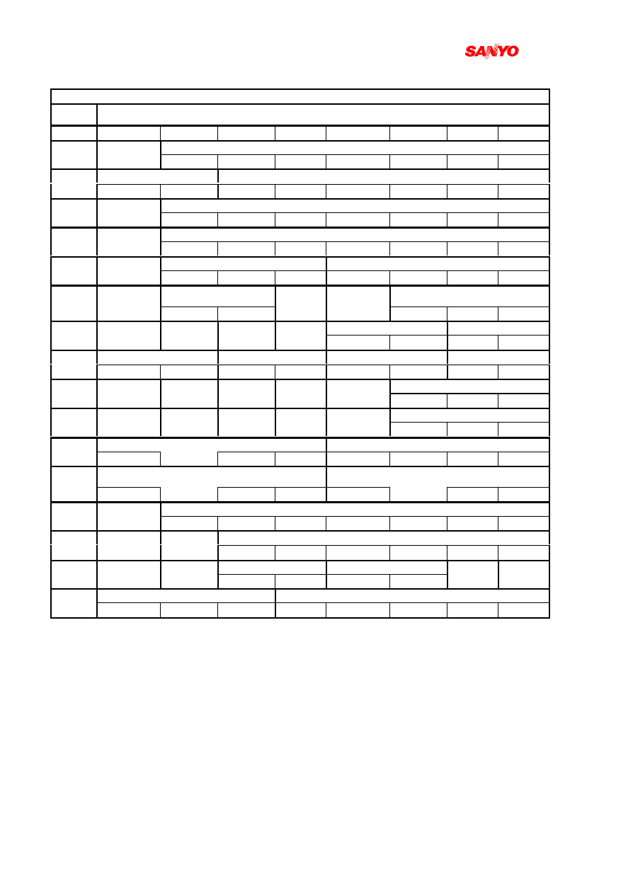
IC Address (Write): 10111010
Control Register Bit Allocations (continued)
Sub
Address
MSB
DATA BITS
LSB
DA0
DA1
DA2
DA3
DA4
DA5
DA6
DA7
00010000 OSD Cnt.Test OSD Contrast
0
1
0
0
0
0
0
0
10001
Coring Gain(W/Defeat)
Sharpness
0
0
0
0
0
0
0
0
10010
Tint.Test
Tint
0
1
0
0
0
0
0
0
10011
Color.Test
Color
0
1
0
0
0
0
0
0
10100
Video SW
Trap Test
Filter.Sys
0
1
0
0
0
0
1
0
10101
Gray Mode
Cross B/W
CbCr_IN
G-Y Angle
Color killer
ope.
0
0
0
0
(0)
0
0
0
10110
VBLK SW
FBPBLK.SW
fsc or Csync
Y_APF
Pre/Over-shoot adj.
W P L Ope. Point(W/Defeat)
0
1
0
0
0
0
0
0
10111 Y Gamma Start
DC.Rest
Blk.Str.start(W/Defeat)
Blk.Str.Gain
0
0
0
0
0
0
0
0
11000
Auto.Flesh
C.Ext
C.Bypass
C_Kill ON
C_Kill OFF
Color.Sys
0
0
1
0
0
0
0
0
11001
Cont.Test
Digital OSD Brt.Abl.Def
Mid.Stp.Def
RGB Temp SW Bright.Abl.Threshold
0
0
0
0
0
1
0
0
11010 R-Y/B-Y Gain Balance
R-Y/B-Y Angle
1
0
0
0
1
0
0
0
11011 B-Y DC Level ( White-
Balance )
R-Y DC Level ( White-
Balance )
1
0
0
0
1
0
0
0
11100 Audio SW
Volume
0
0
0
0
0
0
0
0
11101
IF Test
VOL.FIL
RF.AGC
0
0
1
0
0
0
0
0
11110
FM.Mute
deem.TC
VIF.Sys.SW
SIF.Sys.SW
FM.Gain
IF.AGC
0
0
0
1
0
1
0
0
11111 VIDEO.LEVEL
FM.LEVEL
1
0
0
1
0
0
0
0
(Bits are transmitted in this order.)
Technical Note of LA76818 2001/02/08
46/ 46
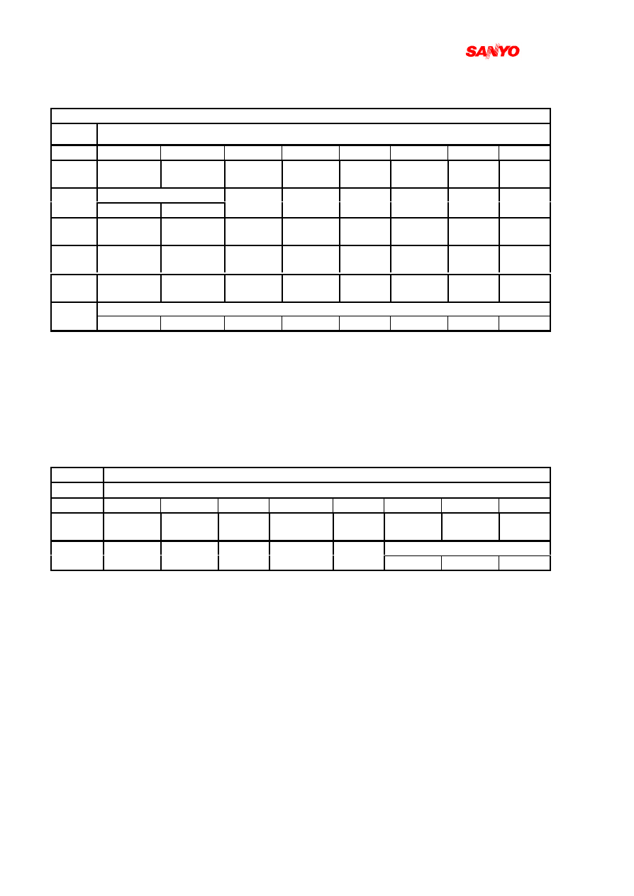
IC Address (Write): 10111010
Control Register Bit Allocations (continued)
Sub
Address
MSB
DATA BITS
LSB
DA0
DA1
DA2
DA3
DA4
DA5
DA6
DA7
00100000
Pre/Over SW* C.VCO Adj SW
*
*
*
*
*
*
0
0
(0)
(0)
(0)
(0)
(0)
(0)
100001
C.VCO Adjust
*
*
*
*
*
*
0
0
(0)
(0)
(0)
(0)
(0)
(0)
100010
*
*
*
*
*
*
*
*
(0)
(0)
(0)
(0)
(0)
(0)
(0)
(0)
100011
*
*
*
*
*
*
*
*
(0)
(0)
(0)
(0)
(0)
(0)
(0)
(0)
100100
*
*
*
*
*
*
*
*
(0)
(0)
(0)
(0)
(0)
(0)
(0)
(0)
100101 IF TEST3
0
1
0
0
1
0
0
0
(Bits are transmitted in this order.)
IC Address (READ): 10111011
Status Register Bit Allocations
MSB
DATA BITS
LSB
DA0
DA1
DA2
DA3
DA4
DA5
DA6
DA7
Status1
*
*
*
RF.AGC
*
V.TRI
50/60
ST/NONST
(0)
(0)
*
*
*
*
*
*
Status2
H.Lock
*
*
Killer
*
Color.Sys
*
(1)
(1)
*
(1)
*
*
*
(Bits are transmitted in this order.)
Wyszukiwarka
Podobne podstrony:
Erisson LA8533xx La76810
więcej podobnych podstron