
SECTION 17
MOUNTING AND SOLDERING
contents
page
INTRODUCTION
17 - 2
AXIAL AND RADIAL LEADED DEVICES
17 - 2
Handling
17 - 2
Soldering
17 - 2
Mounting
17 - 3
SURFACE-MOUNT DEVICES
17 - 3
Reflow soldering process
17 - 3
Double-wave soldering process
17 - 7
Hand soldering of microminiature components
17- 11
Assessment of soldered joint quality
17 - 11
Footprint definitions
17 - 13
Recommended footprints
17 - 14
1996 Oct 15
17 - 2
Philips Semiconductors
Small-signal and Medium-power Diodes
Mounting and soldering
INTRODUCTION
There are two basic forms of electronic component
construction, those with leads for through-hole mounting
and microminiature types for surface mounting.
Through-hole mounting gives a very rugged construction
and uses well established soldering methods. Surface
mounting has the advantages of high packing density plus
high-speed automated assembly.
AXIAL AND RADIAL LEADED DEVICES
The following general rules are for the save handling and
soldering of axial and radial leaded diodes. Special rules
for particular types may apply and, for these, instructions
are given in the individual data sheets. With all
components, excessive forces or heat can cause serious
damage and should always be avoided.
Handling
•
Avoid perpendicular forces on the body of the diode
•
Avoid sudden forces on the leads or body. These forces
are often much greater than allowed
•
Avoid high acceleration as a result of any shock, e.g.
dropping the device on a hard surface
•
During bending, support the leads between body or stud
and the bending point
•
During the bending process, axial forces on the body
must not exceed 20 N
•
Bending the leads through 90
°
is allowed at any
distance from the body when it is possible to support the
leads during bending without contacting the body or
weldings
•
Bending close to the body or stud without supporting the
leads is only allowed if the bend radius is greater than
0.5 mm
•
Twisting the leads is allowed at any distance from the
body or stud only if the lead is properly clamped
between body or stud and the twisting point
•
Without clamping, twisting the leads is allowed only at a
distance of greater than 3 mm from the body; the torque
angle must not exceed 30
°
•
Straightening bent leads is allowed only if the applied
pulling force in the axial direction does not exceed 20 N
and the total pull duration is not longer than 5 s.
Soldering
•
Avoid any force on the body or leads during or
immediately after soldering
•
Do not correct the position of an already soldered device
by pushing, pulling or twisting the body
•
Avoid fast cooling after soldering.
The maximum allowable soldering time is determined by:
•
Package type
•
Mounting environment
•
Soldering method
•
Soldering temperature
•
Distance between the point of soldering and the seal of
the diode body.
Table 1 shows the minimum distances from soldering
point to body seal for components that are mounted on a
printed-wiring board with soldering performed by
hand-held soldering tool, dip, wave or other solder bath
method. The maximum soldering temperature is 300
°
C,
and the maximum soldering time is 5 s.
Table 1
Distance from soldering point to body seal
When soldering is performed by a hand-held soldering tool
on components mounted on anything other than a
printed-wiring board, the minimum distance from body seal
to the soldering point at a maximum soldering temperature
of 300
°
C is stated in Table 1 but the maximum soldering
time must be reduced to 3 s.
PACKAGE
MINIMUM DISTANCE (mm)
SOD27 (DO-35)
0.5
SOD57
0.5
SOD61
2.0
SOD64
0.5
SOD66 (DO-41)
3.0
SOD68 (DO-34)
0.5
SOD81
0.5
SOD83A
0.5
SOD88A
0.5
SOD91
0.5
SOT18/15 (TO-18)
0.5

1996 Oct 15
17 - 3
Philips Semiconductors
Small-signal and Medium-power Diodes
Mounting and soldering
Mounting
If the rules for handling and soldering are observed, the
following mounting or process methods are allowed:
•
Preheating of the printed-wiring board before soldering
up to a maximum of 100
°
C
•
Flat mounting with the diode body in direct contact with
the printed-wiring board with or without metal tracks on
both sides and/or plated-through holes
•
Flat mounting with the diode body in direct contact with
hot spots or hot tracks during soldering
•
Upright mounting with the diode body in direct contact
with the printed-wiring board if the body is not in contact
with metal tracks or plated-through holes.
SURFACE-MOUNT DEVICES
Since the introduction of Surface Mount Devices (SMDs),
component design and manufacturing techniques have
changed almost beyond recognition. Smaller pitch,
minimum footprint area and reduced component volume
all contribute to a more compact circuit assembly. As a
consequence, when designing printed circuit boards
(PCBs), the dimensions of the footprints are perhaps more
crucial than ever before.
One of the first steps in this design process is to consider
which soldering method, either wave or reflow, will be used
during production. This determines not only the solder
footprint dimensions, but also the minimum spacing
between components, the available area underneath the
component where tracks may be laid, and possibly the
required component orientation during soldering.
Although reflow soldering is recommended for SMDs,
many manufacturers use, and will continue to use for some
time to come, a mixture of surface-mount and through-hole
components on one substrate (a mixed print).
The mix of components affects the soldering methods that
can be applied. A substrate having SMDs mounted on one
or both sides but no through-hole components is likely to
be suitable for reflow or wave soldering. A double sided
mixed print that has through-hole components and some
SMDs on one side and densely packed SMDs on the other
normally undergoes a sequential combination of reflow
and wave soldering. When the mixed print has only
through-hole components on one side and all SMDs on the
other, wave soldering is usually applied.
To help with your circuit board design, this guideline gives
an overview of both reflow and wave soldering methods,
and is followed by some useful hints on hand soldering for
repair purposes, and the recommended footprints for our
SMD discrete semiconductor packages.
Reflow soldering process
There are three basic process steps for single-sided PCB
reflow soldering, these are:
1. Applying solder paste to the PCB
2. Component placement
3. Reflow soldering.
A
PPLYING SOLDER PASTE TO THE
PCB
Solder paste can be applied to the PCBs solder lands by
one of either three methods: dispensing, screen or stencil
printing.
Dispensing is flexible but is slow, and only suitable for
pitches of 0.65 mm and above.
With screen printing, a fine-mesh screen is placed over the
PCB and the solder paste is forced through the mesh onto
the solder lands of the PCB. However, because of mesh
aperture limitations (emulsion resolution), this method is
only suitable for solder paste deposits of 300
µ
m and
wider.
Stencil printing is similar to screen printing, except that a
metal stencil is used instead of a fine-mesh screen. The
stencil is usually made of stainless steel or bronze and
should be 150 to 200
µ
m thick. A squeegee is passed
across the stencil to force solder paste through the
apertures in the stencil and onto the solder lands on the
PCB (see Fig.1). It does not suffer from the same
limitations as the other two printing methods and so is the
preferred method currently available.
It is recommended that for solder paste printing, the
equipment is located in a controlled environment
maintained at a temperature of 23
±
2
°
C, and a relative
humidity between 45% and 75%.
1996 Oct 15
17 - 4
Philips Semiconductors
Small-signal and Medium-power Diodes
Mounting and soldering
Stencil printing
The printing process must be able to apply the solder
paste deposits to the PCB:
•
In the correct amounts
•
At the correct position on the lands
•
With an acceptable height and shape.
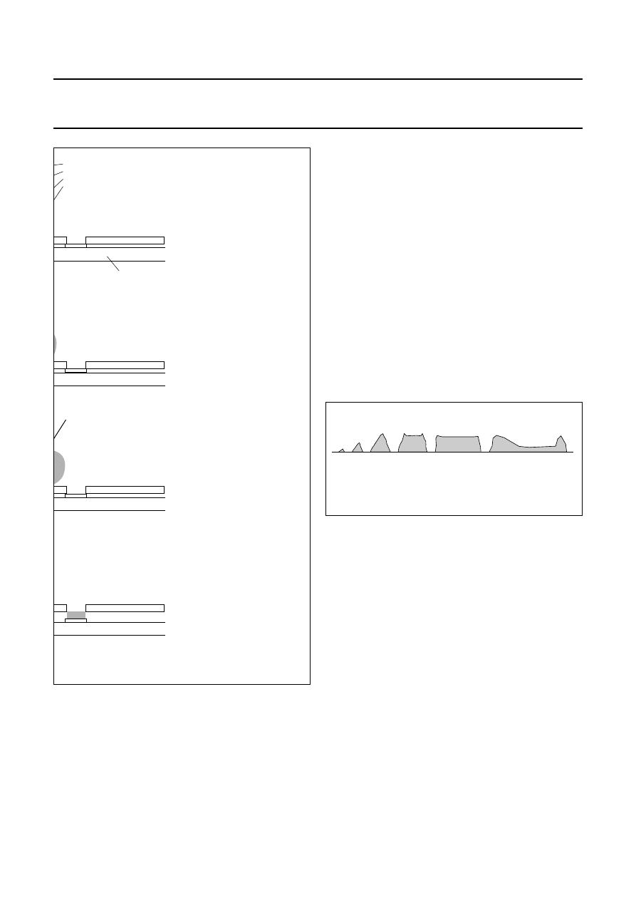
Fig.1 Applying solder paste by stencilling.
,,,,,
MSB905
solder paste
stencil
solder land
board
filling
levelling
release
squeegee
,,
,,
,,,,,
,,,,,
,,
,,,,,
,,
,,,,,
,,,,,
,,
The amount of solder paste used must be sufficient to give
reliable soldered joints. This amount is controlled by the
stencil thickness, aperture dimensions, process settings,
and the volume of paste pressed through the apertures by
the squeegee.
The downward force of the squeegee is counteracted by
the hydrodynamic pressure of the paste, and so the
machine should be set to ensure that the stencil is just
‘cleaned’ by the squeegee.
Suitable aperture dimensions depend on the stencil
thickness. The solder paste deposits must have a flat part
on the top (Fig.2, examples 4 and 5), which can be
achieved by correct process settings. The footprints given
in this book were designed for these correct deposit types.
Stencil apertures that are too small result in irregular dots
on the lands (Fig.2, examples 1 to 3). If the apertures are
too large, solder paste can be scooped out, particularly if a
rubber squeegee is used (Fig.2, example 6).
Ideally, the deposited solder paste should sit entirely on
the solder land. The tolerated misplacement of solder
paste with respect to the solder land is determined by the
most critical component. The solder paste deposit must be
deposited within 100
µ
m with respect to the solder land.
Furthermore, the tackiness (tack strength) of the solder
paste must be sufficient to hold surface-mount devices on
the PCB during assembly and during transport to the
reflow oven. Tack strength depends on factors such as
paste composition, drying conditions, placement pressure,
dwell time and contact area. As a general rule, component
placement should be within four hours after the paste
printing process.
Squeegee
The squeegee can be either metal or rubber. A metal
squeegee gives better overall results and so is
recommended, however with step stencils, a rubber
squeegee has to be used. The footprints given in this
chapter were designed for application by both types of
squeegee.
Fig.2 Shapes of solder deposits for increasing
stencil apertures (left to right).
MSB904
2
1
3
4
5
6
1996 Oct 15
17 - 5
Philips Semiconductors
Small-signal and Medium-power Diodes
Mounting and soldering
Stencil apertures
Stencil apertures can be made by either:
•
Etching
•
Laser cutting
•
Electroforming.
Of the three methods, etching is less accurate as the
deviation in aperture dimensions with respect to the target
is relatively large (target is
+
50
µ
m at squeegee side and
0
µ
m at PCB side).
Laser-cut and electroformed stencils have smaller
deviations in dimensions and are therefore more suitable
for small and fine-pitch components (see Fig.3).
A useful method of controlling the stencil printing process
during production is by monitoring the weight of solder
paste on the board which may vary between 80% and
110% of the theoretical amount according to the target
(designed) apertures. Smearing and clogging of a small
aperture cannot be detected with this method.
Solder paste
Reflow soldering uses a paste consisting of small nodules
of solder and a flux with binder, solvents and additives to
control rheological properties. The flux in the solder paste
can be rosin mildly activated or rosin activated.
The requirements of the solder paste are:
•
Good rolling behaviour
•
No slump during heat-up
•
Low viscosity during printing
•
High viscosity after printing
•
Sufficient tackiness to hold the components
•
Removal of oxides during reflow soldering.
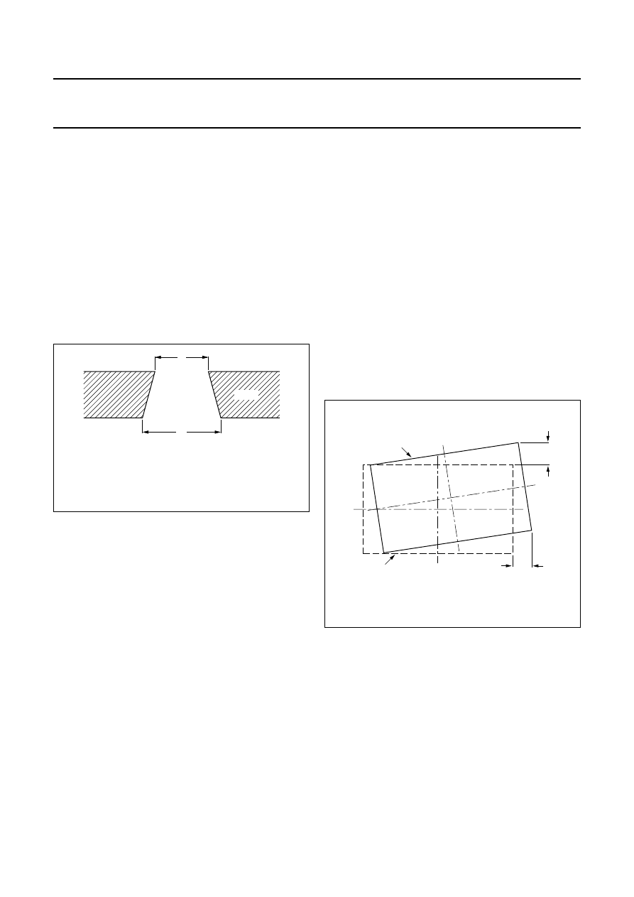
Fig.3 Specifications of laser-cut stencil apertures
for discrete and passive components.
A = B
+
0/
−
30 (
µ
m).
B = X
±
30 (
µ
m).
X = nominal apertures size.
handbook, halfpage
MSB906
B
A
stencil
Suitable solder paste types have the following
compositions:
•
Sn62Pb36Ag2
•
Sn63Pb37
•
Sn60Pb40.
C
OMPONENT PLACEMENT
The position of the component with respect to the solder
lands is an important factor in the final result of the
assembly process. A misaligned component can lead to
unreliable joints, open circuits and/or bridges between
leads.
The placement accuracy is defined as the maximum
permissible deviation of the component outline or
component leads, with respect to the actual position of the
solder land pattern belonging to that component or
component leads on the circuit board (see Fig.4).
A maximum placement deviation (P) of 0.25 mm is used in
these guidelines, which relates to the accuracy of a
low-end placement machine. A higher placement accuracy
is required for components with a fine pitch. This is given
in the footprint description for the components concerned.
Besides the position in x- and y-directions, the z-position
with respect to the solder paste, which is determined by
the placement force, is also important. If the placement
force is too high, solder paste will be squeezed out and
solder balls or bridges will be formed. If the force is too low,
physical contact will be insufficient, leads will not be
soldered properly and the component may shift.
Fig.4 Component placement tolerances.
handbook, halfpage
MSB954
≤
Pcpcu
≤
Pcpcu
target position
related to copper pattern
actual mounted position
1996 Oct 15
17 - 6
Philips Semiconductors
Small-signal and Medium-power Diodes
Mounting and soldering
R
EFLOW SOLDERING
There are several methods available to provide the heat to
reflow the solder paste, such as convection, hot belt, hot
gas, vapour phase and resistance soldering. The preferred
method is, however, convection reflow.
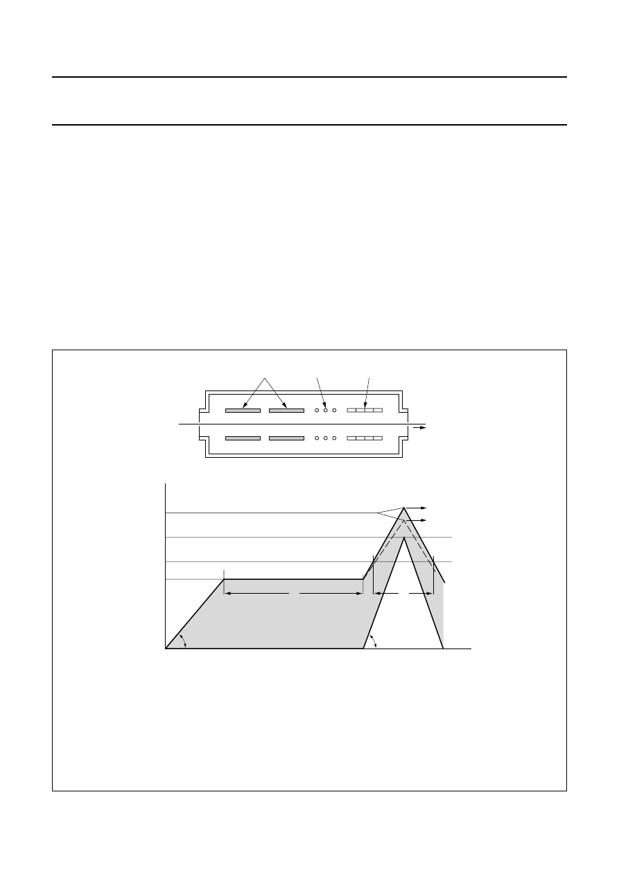
Convection reflow
With this method, the PCBs passes through an oven
where it is preheated, reflow soldered and cooled (see
Fig.5). If the heating rate of the board and components are
similar, however, preheating is not necessary.
During the reflow soldering process, all parts of the board
must be subjected to an accurate temperature/ time
profile. Figure 5 shows a suitable profile framework for
single-sided reflow soldering and the first side of
double-sided print boards. It's important to note that this
profile is for discrete semiconductor packages. The actual
framework for the entire PCB could be smaller than the
one shown, as other components on the board may have
different process requirements.
Reflow soldering can be done in either air or a nitrogen
atmosphere. If soldering in air, the temperature (T
p
) must
not exceed 240
°
C on the first side of a double-sided print
board with organic coated solder lands. This is because
peak temperatures greater than 240
°
C reduce the
solderability of the lands on the second side to be
soldered. This peak temperature can rise to 280
°
C when
soldering the second side with organic coated solder lands
in air.
Fig.5 Convection reflow soldering method (top), process requirements for reflow soldering (bottom).
α
≤
10
°
C/s.
t
E
≤
1 min, if possible (else
≤
5 min).
T
E
≤
160
°
C.
t
M
= 2 to 30 s.
T
R
= 180
°
C.
t
R
≤
70 s.
T
P
min = 205
°
C.
T
p
max = 240
°
C
for soldering the first side of a double-sided
board with organic finish.
T
P
max = 280
°
C
for all other cases.
handbook, full pagewidth
,,,,,,,,,
MLC735
,,,,,,,,,
,,,,,,,,,
preheating
soldering
cooling
belt
handbook, full pagewidth
temperature
Tp max
Tp min
TR
tR
tM
PCB damage
organic finish
affected
time
TE
tE
α
α
MSB976
1996 Oct 15
17 - 7
Philips Semiconductors
Small-signal and Medium-power Diodes
Mounting and soldering
If soldering in a nitrogen atmosphere, a peak temperature
of 280
°
C is allowed for double-sided print boards or
single-sided reflow soldering. Soldering in a nitrogen
atmosphere results in smoother joint meniscus, smaller
contact angles, and better wetting of the copper solder
lands.
The profile can be achieved by correct combinations of
conveyor speed and heater temperature. To check
whether the profile is within specification, the coldest and
hottest spots on the board have to be located.
To do this, you should dispense solder paste deposits
regularly over the surface of a test board and on the
component leads. Set the oven to a moderate temperature
with maximum conveyor velocity and pass the test board
through. If too many solder paste dots melt, lower the
oven's temperature. Continue passing test boards through
the oven, while lowering the speed of the belt in small
steps.
The deposit that melts first indicates the warmest location,
the one that melts last indicates the coldest location. Paste
dots not reflowed after two runs must be replaced by fresh
dots. Thermocouples have to be mounted at the coldest
and warmest location and temperature profiles measured.
Double-wave soldering process
There are four basic process steps for double-wave
soldering, these are:
1. Applying adhesive
2. Component placement
3. Curing adhesive
4. Wave soldering process.
A
PPLYING ADHESIVE
To hold SMDs on the board during wave soldering, it is
necessary to bond the component to the PCB with one or
more adhesive dots. This is done either by dispensing,
stencilling or pin transfer. Dispensing is currently the most
popular technique. It is flexible and allows a controlled
amount of adhesive to be applied at each position.
Stencil printing and pin transfer are less flexible and are
mainly used for mass production. The component-specific
requirements for an adhesive dot are:
•
Shape (volume) of the adhesive dot
•
Number of dots per component
•
Position of the dots.
Volume of adhesive
There must be enough adhesive to keep components in
their correct positions while being transported to the curing
oven. This means that the deposited adhesive must be
higher than the gap between the component and the board
surface. Nevertheless, there should not be too much
deposit as it may smear onto the solder lands, where it can
affect their solderability. The gap between a component
and printed board depends on the geometry of the board
and component (see Fig.6).
Table 2 gives guidelines for volumes of adhesive dots per
package. The spreading in volumes should be within
±
15%.
Table 2
Guidelines for volumes of adhesive dots
COMPONENT
NUMBER OF
DOTS
VOLUME PER
DOT (mm
3
)
SOD106(A)
1
0.65
SOD80(C), SOD87
1
2
0.5
0.08
SOD110, SOD323
2
0.065
SOT323 (SC70-3)
2
0.045
SOT23, SOT143,
SOT 346 (SC59)
2
0.06
SOT89
2
0.3
SOT223
2
0.70
Fig.6 Available space for adhesive between
component and PCB (unmarked area).
h1 = component stand-off height.
h2 = solder resist (and track) height on PCB.
h3 = copper height on PCB.
b1 = gap between solder lands on the PCB.
b2 = gap between metallization of the component.
MSB903
b1
b2
h1
h2
h3
1996 Oct 15
17 - 8
Philips Semiconductors
Small-signal and Medium-power Diodes
Mounting and soldering
Number, position and volume of dots per component
Figure 7 shows the recommended positions and numbers
of adhesive dots for a variety of packages. SOD106(A),
SOT89 and SOT223 packages require much larger
adhesive dots compared with those for other components.
SOD80(C) and SOD87 packages can have one large
adhesive dot (recommended) or two smaller adhesive
dots.
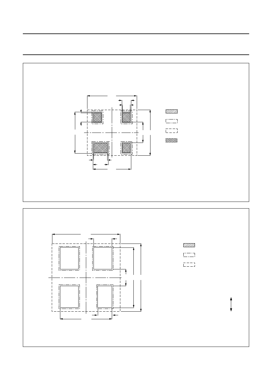
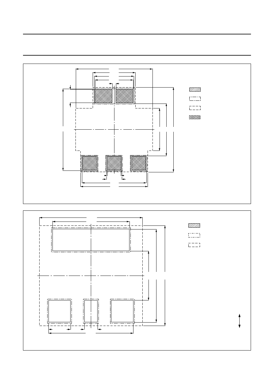
Fig.7 Position of adhesive dots. Pitch between two small dots is 1.0 mm.
For optimum power dissipation, the SOT89 requires a good thermal contact (i.e. good solder joint) between the package and the solder land.
During wave-soldering, however, flux may not always reach the total soldering area beneath the component body, which in turn can lead to an
incomplete solder joint. If the SOT89 is double-wave soldered, therefore, power derating must be applied.
handbook, halfpage
MSB901
handbook, halfpage
MSB900
handbook, halfpage
MSB902
P
handbook, halfpage
MSB899
handbook, halfpage
MSB898
handbook, halfpage
MSB896
handbook, halfpage
MSB897
handbook, halfpage
MSC093
P
a. SOD106(A).
b. SOD80(C), SOD87.
c. SOD110.
d. SOD80(C), SOD87.
e. SOD323.
f. SOT23, SOT143, SOT323 (SC70-3)
SOT346 (SC59).
g. SOT89 (P = 4.4 mm).
h. SOT223 (P = 6.0 mm).
1996 Oct 15
17 - 9
Philips Semiconductors
Small-signal and Medium-power Diodes
Mounting and soldering
Nozzle outlet diameter
Depending on adhesive type and component size, the
nozzle outlet diameter of the dispenser can vary between
0.6 and 0.7 mm for the larger dots, and between
0.3 and 0.5 mm for the smaller dots.
As the rheology of the adhesive is temperature dependent,
the temperature in the nozzle must be carefully controlled
before dispensing. The required temperature depends on
the adhesive type, but is usually between 26
°
C and 32
°
C
to maintain the adhesive's rheology within specification
during dispensing. Thermally curing epoxy adhesives are
normally used.
Adhesives
Beside the nozzle diameters, different adhesive types are
also used for different component sizes.
Small components can be secured during assembly and
wave soldering with a thin (low green strength) adhesive,
which can be dispensed at high speeds. For larger
components (such as QFP and SO packages), a higher
green strength adhesive is required.
C
OMPONENT PLACEMENT
Positioning components on the PCB is similar in practice
to that of reflow soldering.
To prevent component shift and smearing of the adhesive,
board support is important while placing components. This
is particularly important when placing the SOD106(A)
package.
C
URING THE ADHESIVE
To provide sufficient bonding strength between
component and board, the adhesive must be properly
cured. Figure 8 gives general process requirements for
curing most thermosetting epoxy adhesives with latent
hardeners. The temperature profile of all adhesive dots on
the PCB must be within this framework. It's important to
note that this profile is for discrete semiconductor
packages. The actual framework for the entire PCB could
be smaller than the one shown, as other components on
the board may have different process requirements.
To check whether the profile is within specification, the
temperature of coldest and hottest spots must be
measured. The coldest spot is usually under the largest
package: the hottest spot is usually under the smallest
package.
The adhesive can be cured either by infrared or hot-air
convection.
Bonding strength
The bonding strength of glued components on the board
can be checked by measuring the torque force. For small
components the requirements are given in Table 3.
No values are specified for larger packages.
Table 3
Bonding strength requirements
COMPONENT
MINIMUM
BONDING
STRENGTH
(cNcm)
TARGET
BONDING
STRENGTH
(cNcm)
SOD323, SOD110,
SOT323 (SC70-3)
110
250
SOD80(C), SOD87
200
350
SOT23, SOT346 (SC59),
SOT143
150
250
Fig.8 Process requirements for curing
thermosetting adhesives.
T
max
≤
160
°
C.
T
min
≥
110
°
C.
t
C
≥
3 minutes.
α
≤
100
°
C/min (some adhesives allow higher heating rates).
If T
min
> 125
°
C, t
C
may be <3 min, depending on adhesive
specification.
temperature
Tmin
Tmax
time
α
MSB977
tC
1996 Oct 15
17 - 10
Philips Semiconductors
Small-signal and Medium-power Diodes
Mounting and soldering
W
AVE SOLDERING PROCESS
After applying adhesive, placing the component on the
PCB and curing, the PCB can be wave soldered. The wave
soldering process is basically built up from three
sub-processes. These are:
1. Fluxing
2. Preheating
3. (Double) wave soldering.
Although listed here as sub-process they are in practice
combined in one machine. All are served by one transport
mechanism, which guides the PCBs at an incline through
the soldering machine. It's important to note that the PCB
must be loaded into the machine so that the SMDs on the
board come into direct contact with the solder wave (see
Fig.9).
In principle, two different systems of PCB transports are
available for wave soldering:
•
Carrier transport
PCBs are mounted on a soldering carrier, which moves
through the soldering machine, taking it from one
sub-process to the next. The advantage of carrier
mounting is that the board is fixed and warpage during
soldering is reduced.
•
Carrierless transport
PCBs are guided through the soldering machine by a
chain with grips. This method is more convenient for
mass production.
Fluxing
Fluxing is necessary to promote wetting both of the PCB
and the mounted components. This ensures a good and
even solder joint.
Fig.9 Double-wave soldering.
MSC029
solder
During the fluxing process, the solder side of the PCB
(including the components) are covered with a thin layer of
solder flux, which can be applied to the PCB either by
spraying or as a foam. Although several types of solder
flux are available for this purpose, they can be categorized
into three main groups:
•
Non-activated flux (e.g. rosin-based fluxes)
•
Mildly activated flux (e.g. rosin-based or synthetic
fluxes)
•
Highly activated flux (e.g. water-soluble fluxes).
The choice for a particular flux type depends mainly on the
products to be soldered.
Although there is always some flux residue left on the PCB
after soldering, it's not always necessary to wash the
boards to remove it. Whether to clean the board can
depend on:
•
The type of flux used (highly activated fluxes are
corrosive and so should always be removed).
•
The required appearance of the board after soldering.
•
Customer requirements.
Preheating
After the flux is applied, the PCB needs to be preheated.
This serves several purposes: it evaporates the flux
solvents, it accelerates the activity of the flux and it heats
the PCB and components to reduce thermal shock.
The required pre-heat temperature depends on the type of
flux used. For example, the more common low-residue
fluxes require a pre-heat temperature of 120
°
C
(measured on the wave solder side of the PCB).
(Double) wave soldering
The PCB first passes over a highly intensive (jet) solder
wave with a carefully controlled constant height. This
ensures good contact with the PCB, the edges of SMDs
and the leads of components near to high non-wetted
bodies. The greater the board's immersion depth into this
first wave, the fewer joints will be missed.
If the PCB is carrier mounted, the first wave’s height, and
thus the board's immersion depth, can be greater.
Carrierless soldering is more convenient for mass
production, but the height of the wave must be lower to
avoid solder overflowing to the top side of the board. The
height of the jet wave is given in Table 4 along with an
indication of soldering process window. This information is
based on a 1.6 mm thick PCB.
1996 Oct 15
17 - 11
Philips Semiconductors
Small-signal and Medium-power Diodes
Mounting and soldering
The second, smoother laminar solder wave completes
formation of the solder fillet, giving an optimal soldered
connection between component and PCB. It also reduces
the possibility of solder bridging by taking up excessive
solder.
To reduce lead/tin oxides and possibly other solder
imperfection forming during soldering, the complete wave
configuration can be encapsulated by an inert atmosphere
such as nitrogen.
Hand soldering microminiature components
It is possible to solder microminiature components with a
light-weight hand-held soldering iron, but this method has
obvious drawbacks and should be restricted to laboratory
use and/or incidental repairs on production circuits:
•
Hand-soldering is time-consuming and therefore
expensive
•
The component cannot be positioned accurately and the
connecting tags may come into contact with the
substrate and damage it
•
There is a risk of breaking the substrate and internal
connections in the component could be damaged
•
The component package could be damaged by the iron.
Assessment of soldered joint quality
The quality of a soldered joint is assessed by inspecting
the shape and appearance of the joint. This inspection is
normally done with either a low-powered magnifier or
microscope, however where ultra-high reliability is
required, video, X-ray or laser inspection equipment may
be considered.
Both sides of the PCB should be carefully examined: there
should be no misaligned, missing or damaged
components, soldered joints should be clean and have a
similar appearance, there should be no solder bridging or
residue, and the PCB should be assessed for general
cleanliness.
Unlike leaded component joints where the lead also
provides added mechanical strength, the SMD relies on
the quality of the soldering for both electrical and
mechanical integrity. It is therefore necessary that the
inspector is trained to make a visual assessment with
regard to long-term reliability.
Criteria used to assess the quality of an SMD solder joint
include:
•
Correct position of the component on the solder lands
•
Good wetting of the surfaces
•
Correct amount of solder
•
A sound, smooth joint surface.
Table 4
Process ranges for carrierless and carrier double wave soldering
CARRIERLESS
CARRIER
Preheat temperature of board at wave solder side (
°
C)
120
±
10
Heating rate preheating (
°
C/s)
∆
T/
∆
t
≤
3
First (jet) wave:
wave height with respect to bottom side of board (mm)
1.6
+
0.5/
−
0
3.0
+
0.5/
−
0
Second (laminar) wave (double sided overflow):
height with respect to underside of the board (mm)
0.8
+
0.5/
−
0
relative stream velocity with respect to the board
0
Solder temperature (
°
C)
250
±
3
Contact times (s):
first (jet) wave
0.5
+
0.5/
−
0
second (laminar) wave
2.0
±
0.2 (plain holes); 2.5
±
0.2 (plated holes)
PCB transport angle (
°
)
7
±
0.5
Solder alloys
Sn60Pb40; Sn60Pb38Bi2
1996 Oct 15
17 - 12
Philips Semiconductors
Small-signal and Medium-power Diodes
Mounting and soldering
P
OSITIONING
If a lead projects over the solder land too far an unreliable
joint is obtained. Figures 10 to 12 show the maximum shift
allowed for various components. The dimensions of these
solder lands guarantee that, in the statistically extreme
situation, a reliable soldered joint can be made.
G
OOD WETTING
This produces an even flow of solder over the surface land
and component lead, and thinning towards the edges of
the joint. The metallic interaction that takes place during
soldering should give a smooth, unbroken, adherent layer
of solder on the joint.
C
ORRECT AMOUNT OF SOLDER
A good soldered joint should have neither too much nor too
little solder: there should be enough solder to ensure
electrical and mechanical integrity, but not so much that it
causes solder bridging.
S
OUND
,
SMOOTH JOINT SURFACE
The surface of the solder should be smooth and
continuous. Small irregularities on the solder surface are
acceptable, but cracks are unacceptable.
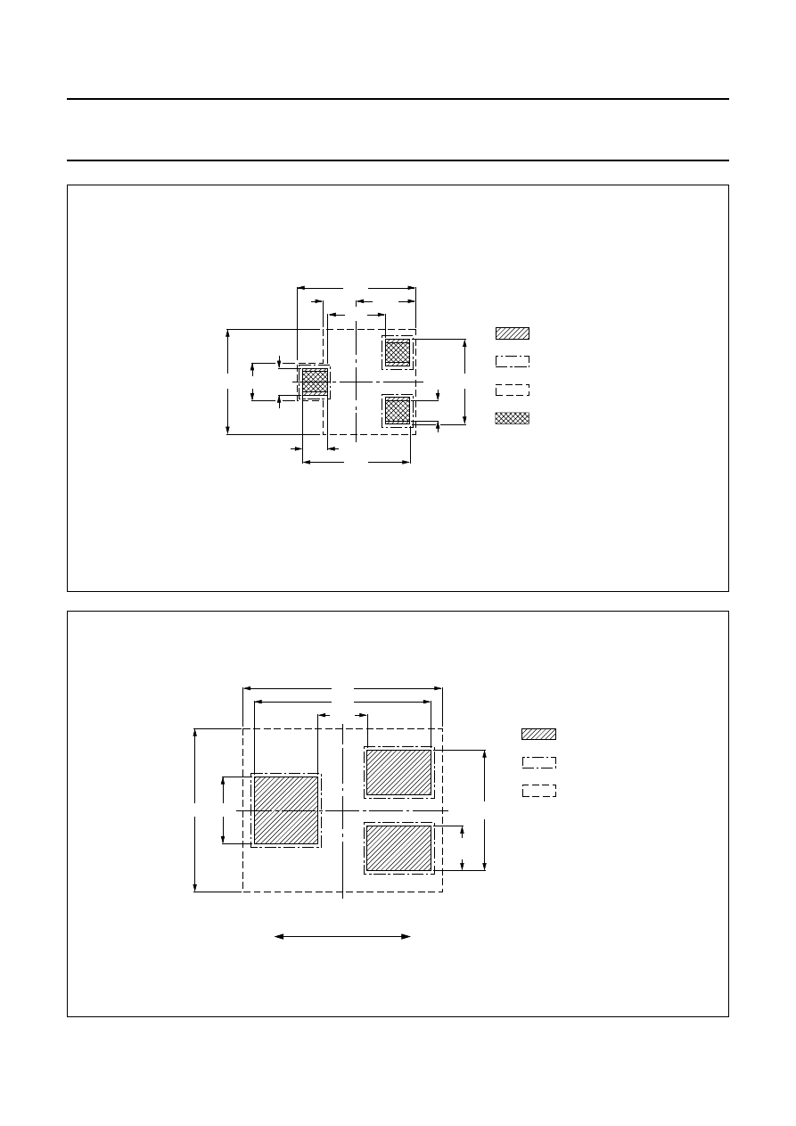
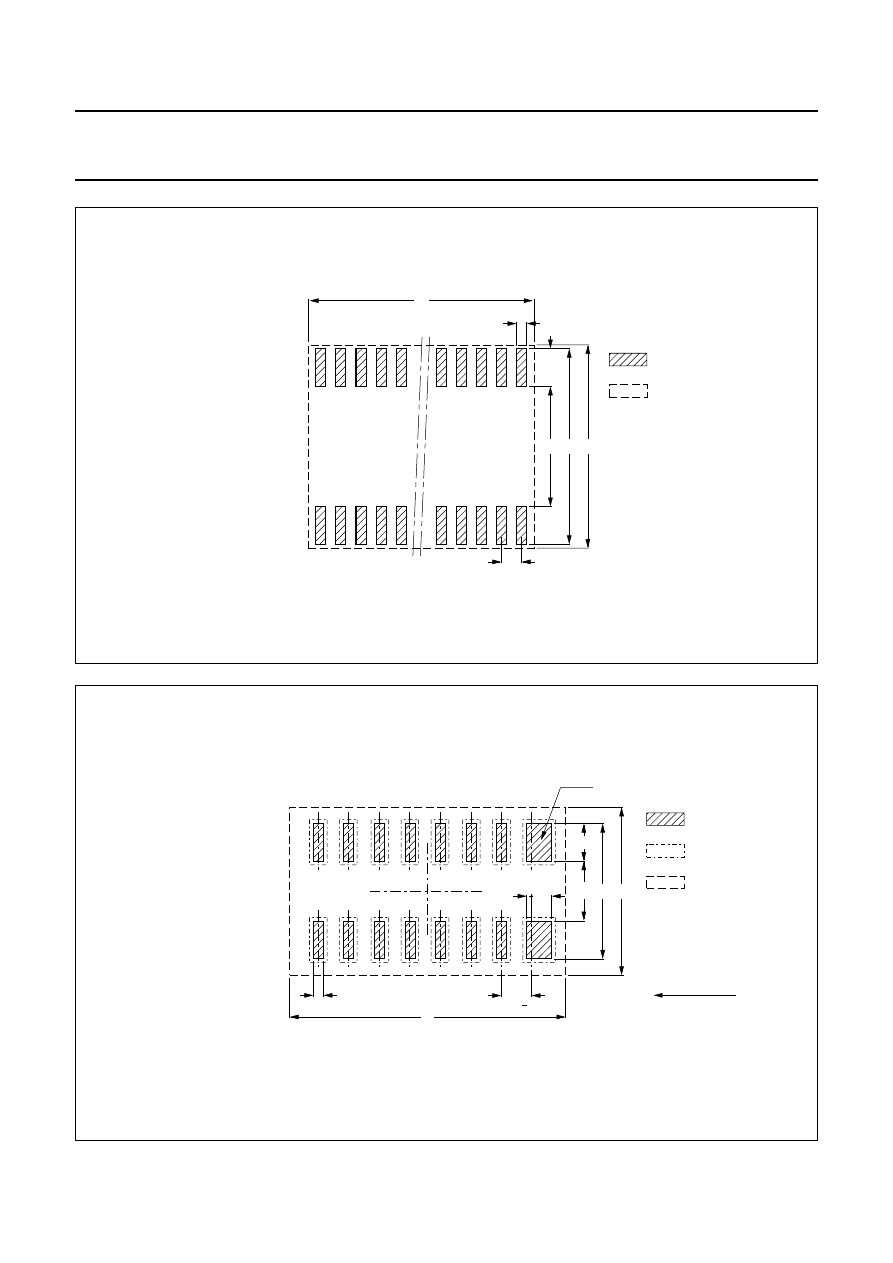
Fig.10 J
≥
0.3 mm.
handbook, halfpage
,,,
,,,
,,,
,,,
,,,
,,,
,,,
,,,
MSB963
J
solder lands
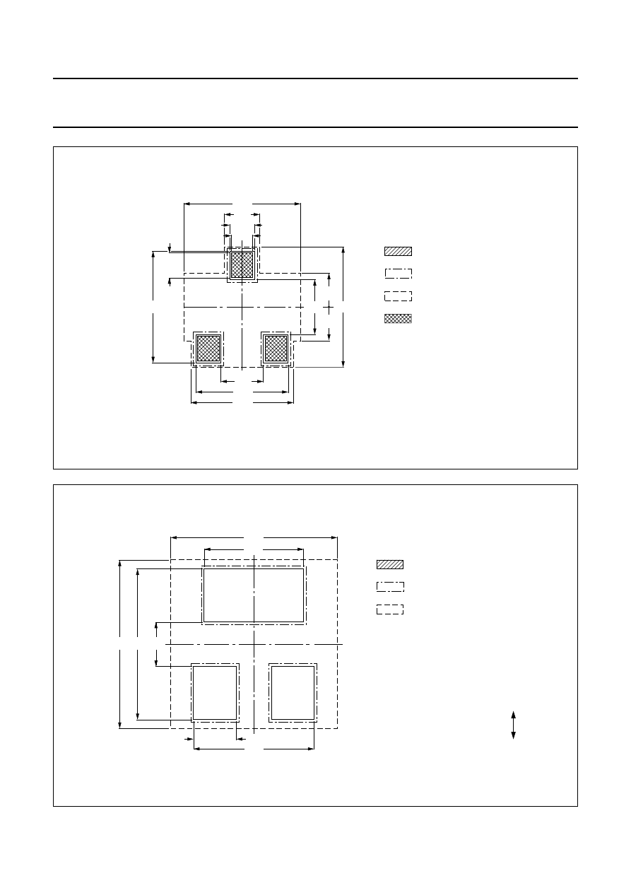
Fig.11 J
≥
0.1 mm; solder land > L
p
.
handbook, halfpage
,,,,
,,,,
MSB964
Lp
J
>
0.1 mm
0.25 mm
printed board
Fig.12 Oc > half lead width.
handbook, full pagewidth
,,
,,
,,
,,
,,
,,
,,
,,
,,,,
,,,,
MSB955
,,,,,,,
,,,,,,,
Lp
Jcucp
>
0.1 mm
Jcucp
0.25 mm
printed board
printed board
Ocpcu
nom. pos.
extreme pos.
solder lands
1996 Oct 15
17 - 13
Philips Semiconductors
Small-signal and Medium-power Diodes
Mounting and soldering
Footprint definitions
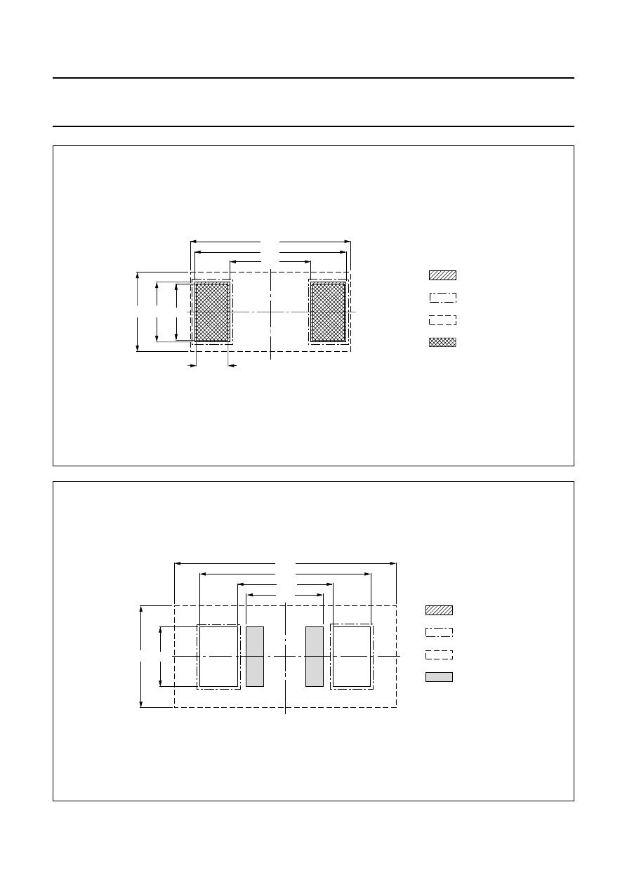
A typical SMD footprint, is composed of:
•
Solder lands (conductive pattern)
•
Solder resist pattern
•
Occupied area of the component
•
Solder paste pattern (for reflow soldering only)
•
Area underneath the SMD available for tracks
•
Component orientation during wave soldering.
S
OLDER LANDS
(
CONDUCTIVE PATTERN
)
The dimensions of the solder lands given in these
guidelines are the actual dimensions of the conductive
pattern on the printed board (see Fig.13).
These dimensions are more crucial for fine-pitch
components.
S
OLDER RESIST PATTERN
The solder resist on the circuit board prevents short
circuits during soldering, increases the insulation
resistance between adjacent circuit details and stops
solder flowing away from solder lands during reflow
soldering.
The solder land dimensions are designed to give optimum soldering
results. They do not take into account the copper area for optimum
power dissipation. If an extra area is required to improve power
dissipation, it should be coated with solder resist. This is especially
important for power packages such as SOD106(A), SOT89 and
SOT223.
handbook, halfpage
MSB956
,,,,,,,,
,,,,,,,,
design width (
+
0.04. . .
−
0.4)
design width (0. . .
−
0.07)
solder land width
Fig.13 Requirements of solder land dimensions.
In contrast to the tracks, which must be entirely covered,
solder lands must be free of solder resist. Because of this,
the cut-outs in the solder resist pattern should be at least
0.15 mm or 0.3 mm larger than the relevant solder lands
(for a photo-defined and screen printed solder resist
pattern respectively). The solder resist cut-outs given with
the footprints in these guidelines are sketched and their
dimensions can be calculated by using the above rule.
Consult your printed board supplier for agreement with
these solder resist cut-outs.
O
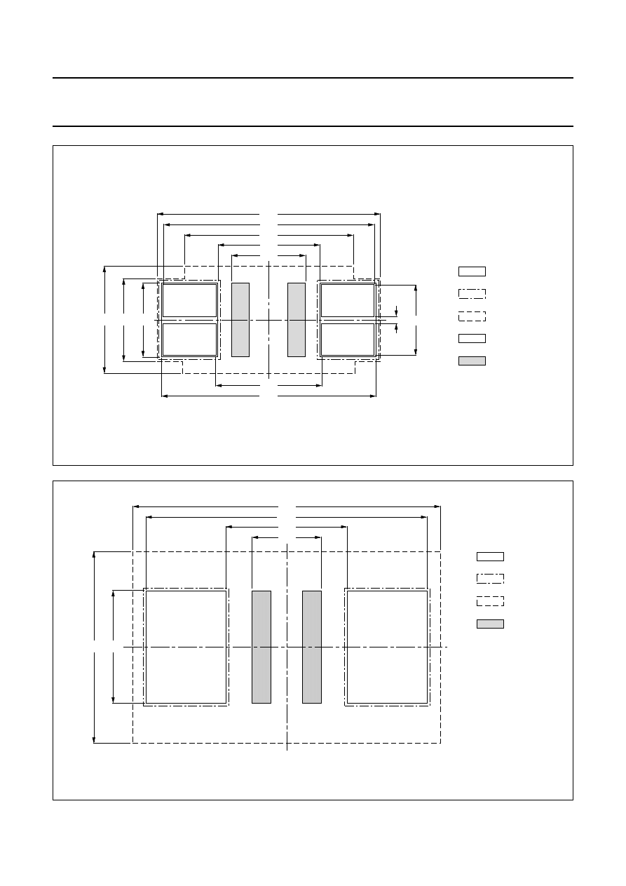
CCUPIED AREA OF THE COMPONENT
A minimum spacing between components is necessary to
avoid component placement problems, short circuits
during wave or reflow soldering and dry solder joints during
wave soldering caused by non-wettable component
bodies. These problems can be avoided by placing the
components so the occupied areas do not overlap (see
Fig.14).
Fig.14 Minimum spacing required (bottom)
between components.
handbook, full pagewidth
MSB958
,,
,,
,,
,,
,,
,,
,,
,,
,,
,,
,,
,,
,,
,,
,,,
,,,
,,
,,
CORRECT
WRONG
1996 Oct 15
17 - 14
Philips Semiconductors
Small-signal and Medium-power Diodes
Mounting and soldering
S
OLDER PASTE PATTERN
It is important to use a solder paste printer which is optical
aligned with the PCBs copper pattern for the reflow
footprints presented here. This is because, for these
footprints, the solder paste deposit must be within a
0.1 mm tolerance with respect to the copper pattern.
To ensure the right amount of solder for each solder joint,
the stencil apertures must be equal to the solder paste
areas given by the footprints.
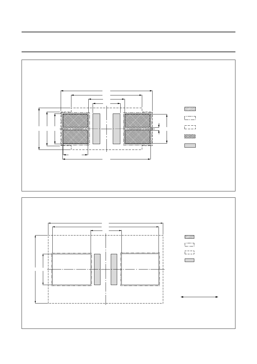
A
REA AVAILABLE FOR TRACKS
(
CONDUCTIVE PATTERN
)
Tracks underneath leadless SMDs must be covered with
solder resist. However, as solder resist can sometimes be
thin or have pin holes at the edges of tracks (especially
when applied by screen printing), an additional clearance
for tracks with respect to the actual metallization position
of the mounted component should be taken into account
(see Fig.15).
For components that need the additional clearance, the
footprints on the following pages give the maximum space
for tracks not connected to the solder lands
(clearance
≥
0.1 mm), for low-voltage applications.
The number of tracks in this space is determined by the
specified line resolution of the printed board.
Fig.15 Clearance required underneath component
between metallization and tracks.
handbook, halfpage
MSB957
tracks
clearence
solder resist
component
C
OMPONENT ORIENTATION DURING WAVE SOLDERING
Where applicable, footprints for wave soldering are given
with the transport direction of the PCB. This is given as
either a ‘preferred transport direction during soldering’ or
‘transport direction during soldering’.
Components with small terminals and non-wettable
bodies, have a smaller risk of dry joints, especially when
using carrierless soldering as the components are placed
according to the ‘preferred orientation’.
Components have no orientation preference for reflow
soldering.
Recommended footprints
The recommended footprints for our discrete
semiconductor packages are given on the following pages.
For their dimensional outline drawings, see the ‘Package
outlines’ section at the end of this book.
In addition to its standard footprints, SOD110 has a reflow
footprint for high thermal cycling load applications (see
Fig.16). This footprint has larger solder lands to give a
fatter solder fillet and, therefore, longer solder fatigue life.
A SOD110 mounted on this footprint has a lower
self-aligning ability, and has a higher risk of displacement
when soldered in a nitrogen atmosphere.
Fig.16 Reflow soldering footprint for SOD110
(high thermal cycling load).
MSA459
,,,
,,,
,,,
1.00
1.10
2.90
3.00
3.60
1.15
1.25
1.65
,,
,,
,,
solder lands
solder resist
occupied area
solder paste
,,
,,
,,,
,,,
1996 Oct 15
17 - 15
Philips Semiconductors
Small-signal and Medium-power Diodes
Mounting and soldering
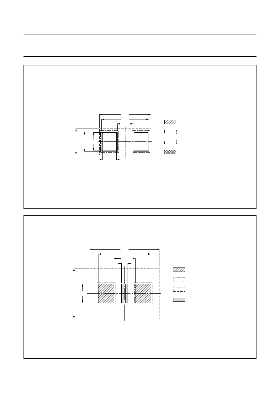
Fig.17 Reflow soldering footprint for SOD80(C).
handbook, full pagewidth
MSA435
2.30
4.30
4.55
1.60
1.70
2.25
0.90
(2x)
solder lands
solder resist
occupied area
solder paste
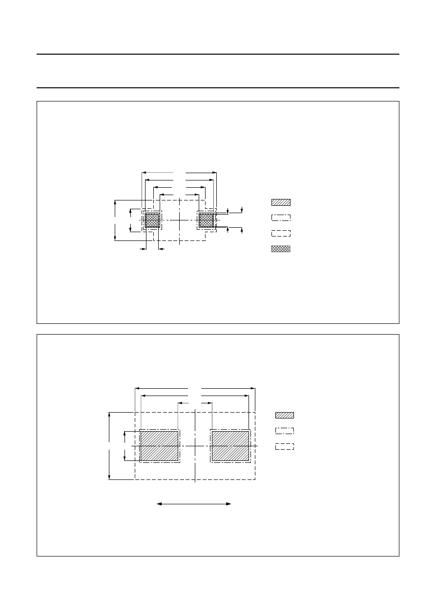
Fig.18 Wave soldering footprint for SOD80(C).
handbook, full pagewidth
MSA461
,,
,,
,,
,,
2.70
4.90
6.30
1.70
2.90
,,
,,
,,
,,
solder lands
solder resist
occupied area
1.90
tracks
1996 Oct 15
17 - 16
Philips Semiconductors
Small-signal and Medium-power Diodes
Mounting and soldering
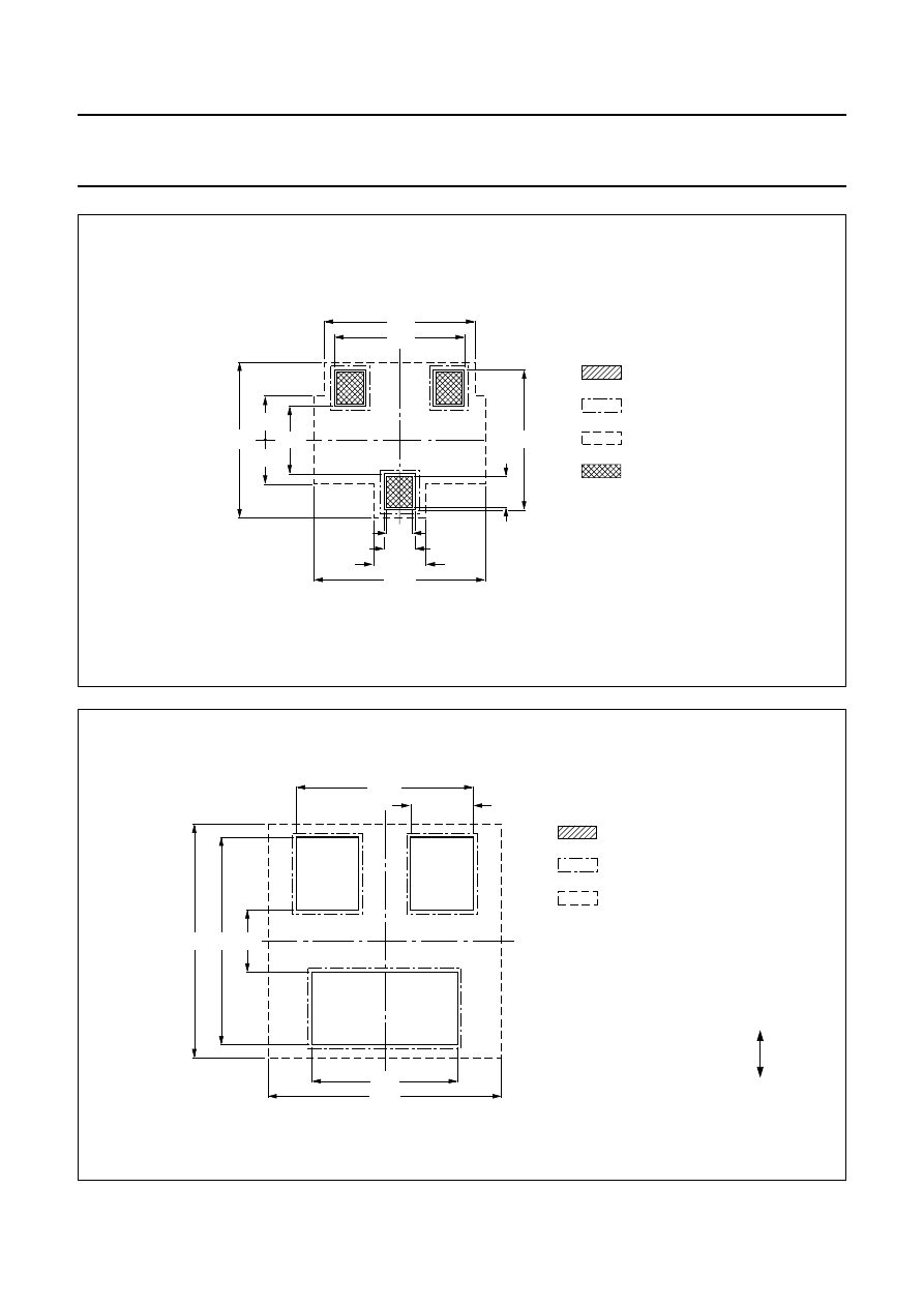
Fig.19 Reflow soldering footprint for SOD87.
handbook, full pagewidth
MSA436
2.30
4.30
4.55
1.80
1.90
2.80
0.90
(2x)
solder lands
solder resist
occupied area
solder paste
0.20
,,
,,
,,
,,
,,
,,
,,
,,
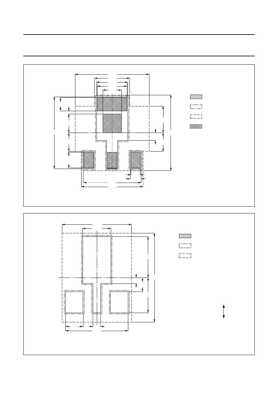
Fig.20 Wave soldering footprint for SOD87.
handbook, full pagewidth
MSA417
2.30
5.40
6.80
2.00
4.60
solder lands
solder resist
occupied area
1.90
tracks
1996 Oct 15
17 - 17
Philips Semiconductors
Small-signal and Medium-power Diodes
Mounting and soldering
Fig.21 Reflow soldering footprint for SOD106.
handbook, full pagewidth
MBH648
2.90
4.80
6.00
6.35
2.10
2.35
3.00
,,,
,,,
,,,
,,,
,,,
,,,
,,,
,,,
,,,
,,,
3.05
2.10
6.10
0.20
2.00
,,
solder lands
solder resist
occupied area
solder paste
occupied area
,,
,,
,,,
,,,
,,,
,,,
,,,
,,,
,,,
,,,
,,,
,,,
Fig.22 Wave soldering footprint for SOD106.
handbook, full pagewidth
,,,,,
,,,,,
,,,,,
,,,,,
,,,,,
,,,,,
,,,,,
,,,,,
,,,,,
,,,,,
,,,,,
,,,,,
MBH647
3.45
1.95
8.05
3.20
5.45
8.75
,,
solder lands
solder resist
occupied area
tracks
1996 Oct 15
17 - 18
Philips Semiconductors
Small-signal and Medium-power Diodes
Mounting and soldering
Fig.23 Reflow soldering footprint for SOD106(A).
handbook, full pagewidth
MSA437
2.50
4.90
6.35
2.10
2.35
1.70 (2x)
2.90
1.90
6.10
0.20
2.00
solder lands
solder resist
occupied area
solder paste
occupied area
Fig.24 Wave soldering footprint for SOD106(A).
handbook, full pagewidth
MSA458
,,,,,,
,,,,,,
,,,,,,
,,,,,,
,,,,,,
,,,,,
,,,,,
,,,,,
,,,,,
,,,,,
2.40
8.60
9.30
2.50
5.50
solder lands
solder resist
occupied area
tracks
preferred transport direction during soldering
1996 Oct 15
17 - 19
Philips Semiconductors
Small-signal and Medium-power Diodes
Mounting and soldering
Fig.25 Reflow soldering footprint for SOD110.
handbook, full pagewidth
MSA460
,,,
,,,
,,,
1.10
0.70
2.70
3.10
0.90
1.00
1.65
,,
,,
,,
solder lands
solder resist
occupied area
solder paste
,,
,,
,,,
,,,
Fig.26 Wave soldering footprint for SOD 110.
handbook, full pagewidth
MSA428
1.35
3.35
4.45
1.20
3.20
0.40
solder lands
solder resist
occupied area
tracks
1996 Oct 15
17 - 20
Philips Semiconductors
Small-signal and Medium-power Diodes
Mounting and soldering
Fig.27 Reflow soldering footprint for SOD323.
handbook, full pagewidth
MSA433
1.65
0.50
(2x)
2.10
1.60
2.80
0.60
3.05
0.50
0.95
solder lands
solder resist
occupied area
solder paste
Fig.28 Wave soldering footprint for SOD323.
handbook, full pagewidth
MSA415
1.40
4.40
5.00
1.20
2.75
solder lands
solder resist
occupied area
preferred transport direction during soldering
1996 Oct 15
17 - 21
Philips Semiconductors
Small-signal and Medium-power Diodes
Mounting and soldering
Fig.29 Reflow soldering footprint for SOT23.
handbook, full pagewidth
,
,
MSA439
1.00
0.60
(3x)
1.30
1
2
3
2.50
3.00
0.85
2.70
,,
,,
,,
,,
2.90
0.50 (3x)
0.60 (3x)
3.30
0.85
solder lands
solder resist
occupied area
solder paste
Fig.30 Wave soldering footprint for SOT23.
handbook, full pagewidth
MSA427
4.00
4.60
2.80
4.50
1.20
,,,,
,,,,
,,,,
,,,
,,,
,,,
,,,
,,,
,,,
3.40
3
2
1
1.20 (2x)
preferred transport direction during soldering
solder lands
solder resist
occupied area
1996 Oct 15
17 - 22
Philips Semiconductors
Small-signal and Medium-power Diodes
Mounting and soldering
Fig.31 Reflow soldering footprint for SOT89.
handbook, full pagewidth
MSA442
1.00
(3x)
4.85
4.60
1.20
4.75
0.60 (3x)
0.70 (3x)
,,,,
,,,,
,,,,
,,,,
,,,,
,,,,
,,,,
,,
,,
,,
,,
,,
,,
3.70
3.95
1.20
0.50
1.70
1
2
3
0.20
0.85
1.20
1.20
1.90
2.00
2.25
solder lands
solder resist
occupied area
solder paste
Fig.32 Wave soldering footprint for SOT89.
Not recommended for wave soldering (see Fig.7).
handbook, full pagewidth
MSA423
3.00
7.60
6.60
1.20
5.30
1.50
,,,
,,,
,,,
,,,
,,,
,,,
,,,
,,,
0.50
3.50
2.40
1
2
3
0.70
,,,
,,,
,,,
,,,
,,,
,,,
solder lands
solder resist
occupied area
transport direction during soldering
1996 Oct 15
17 - 23
Philips Semiconductors
Small-signal and Medium-power Diodes
Mounting and soldering
Fig.33 Reflow soldering footprint for SOT143 (footprint for SOT143R is mirror image).
handbook, full pagewidth
,,
,,
MSA441
0.60
(4x)
1.30
2.50
3.00
2.70
0.50 (3x)
0.60 (3x)
3.25
4
3
2
1
,,
,,
,,
,,
,,
,,
0.90
1.00
solder lands
solder resist
occupied area
solder paste
Fig.34 Wave soldering footprint for SOT143 (footprint for SOT143R is mirror image).
ndbook, full pagewidth
MSA422
4.00 4.60
1.20 (3x)
4.45
1
2
3
4
1.15
,,
,,
,,
3.40
1.00
preferred transport direction during soldering
,,
,,
,,
,,
,,
,,
,,
,,
,,
solder lands
solder resist
occupied area
1996 Oct 15
17 - 24
Philips Semiconductors
Small-signal and Medium-power Diodes
Mounting and soldering
Fig.35 Reflow soldering footprint for SOT223.
handbook, full pagewidth
MSA443
1.20
(4x)
3.90
5.90
4.80
7.40
4
2
3
1
3.85
1.20 (3x)
1.30 (3x)
,,
,,
,,
,,
,,
,,
,,,,
,,,,
0.30
3.60
3.50
7.00
6.15
7.65
solder lands
solder resist
occupied area
solder paste
Fig.36 Wave soldering footprint for SOT223.
handbook, full pagewidth
MSA424
8.70
8.90
7.30
1.90 (2x)
6.70
4
1
2
3
1.10
,,,,,,,
,,,,,,,
,,,,,,,
,,,
,,,
,,,
,,
,,
,,
,,,
,,,
,,,
8.10
4.30
preferred transport direction during soldering
solder lands
solder resist
occupied area
1996 Oct 15
17 - 25
Philips Semiconductors
Small-signal and Medium-power Diodes
Mounting and soldering
Fig.37 Reflow soldering footprint for SOT323 and SC70-3.
handbook, full pagewidth
MSA429
0.85
2.35
0.55
(3x)
1.325
0.75
2.40
2.65
1.30
3
2
1
0.60
(3x)
0.50
(3x)
1.90
solder lands
solder resist
occupied area
solder paste
Fig.38 Wave soldering footprint for SOT323 and SC70-3.
handbook, full pagewidth
MSA419
4.00
4.60
2.10
3.65
1.15
2.70
3
2
1
0.90
(2x)
preferred transport direction during soldering
solder lands
solder resist
occupied area
1996 Oct 15
17 - 26
Philips Semiconductors
Small-signal and Medium-power Diodes
Mounting and soldering
Fig.39 Reflow soldering footprint for SOT346 (SC59).
handbook, full pagewidth
,,
,,
MSA440
1.00
0.70
(3x)
1.55
2.60
3.40
0.95
3.15
3
1
2
1.20
0.60 (3x)
0.70 (3x)
3.30
0.95
,
,
,,
,,
2.90
solder lands
solder resist
occupied area
solder paste
Fig.40 Wave soldering footprint for SOT346 (SC59).
book, full pagewidth
MSA420
4.60
5.20
2.80
4.70
1
2
3
1.20
,,,,,
,,,,,
,,,,,
,,
,,
,,
,,
,,
,,
3.40
1.20 (2x)
preferred transport direction during soldering
solder lands
solder resist
occupied area
1996 Oct 15
17 - 27
Philips Semiconductors
Small-signal and Medium-power Diodes
Mounting and soldering
Fig.41 Reflow soldering footprint for SO20 (SOT163-1)
handbook, full pagewidth
MSB461
1.27
0.60
G
B
A
F
C
solder lands
occupied area
Dimensions:
A = 11.00 mm
B =
8.00 mm
C =
1.50 mm
F = 11.40 mm
G = 13.40 mm
placement accuracy = 0.25 mm
Fig.42 Wave soldering footprint for SO20 (SOT163-1)
handbook, full pagewidth
MLC745
G
1.20
0.3
A
B
F
C
solder lands
solder resist
occupied area
1.27 (N 2)X
0.60
enlarged solder land
board direction
Dimensions:
A = 11.50 mm
B =
7.90 mm
C =
1.80 mm
F = 13.00 mm
G = 15.90 mm
N = 20
placement accuracy = 0.25 mm

1996 Oct 15
17 - 28
Philips Semiconductors
Small-signal and Medium-power Diodes
Mounting and soldering
Wyszukiwarka
Podobne podstrony:
SC01 MARKING 1996 1
06 1996 55 58
1996 06 25 1147
1996 10 26 praid 18571 Nieznany
1996 07 23 1433
Autonomia Palestyńska 1996 2005
09 1996 3
MAZDA PROTEGE 1996(1)
09 1996 31 35
10 1996 83 84
1996 (102)
01 1996 57 60
01 1996 4 5
02 1996 81 84
1996 02 14 0282
1996 09 17 1798
08 1996 9 13
03 1996 3
08 1996 63 67
więcej podobnych podstron