
© 2007 Microchip Technology Inc.
DS01114A -page 1
AN1114
INTRODUCTION
The industry drive toward smaller, lighter and more
efficient electronics has led to the development of the
Switch Mode Power Supply (SMPS). There are several
topologies commonly used to implement SMPS.
This application note, which is the first of a two-part
series, explains the basics of different SMPS
topologies. Applications of different topologies and
their pros and cons are also discussed in detail. This
application note will guide the user to select an
appropriate topology for a given application, while
providing useful information regarding selection of
electrical and electronic components for a given SMPS
design.
WHY SMPS?
The main idea behind a switch mode power supply can
easily be understood from the conceptual explanation
of a DC-to-DC converter, as shown in Figure 1. The
load, R
L
, needs to be supplied with a constant voltage,
V
OUT
, which is derived from a primary voltage source,
V
IN
. As shown in Figure 1, the output voltage V
OUT
can
be regulated by varying the series resistor (R
S
) or the
shunt current (I
S
).
When V
OUT
is controlled by varying I
S
and keeping R
S
constant, power loss inside the converter occurs. This
type of converter is known as shunt-controlled
regulator. The power loss inside the converter is given
by Equation 1. Please note that the power loss cannot
be eliminated even if I
S
becomes zero.
FIGURE 1:
DC-DC CONVERTER
EQUATION 1:
SHUNT-CONTROLLED
REGULATOR POWER LOSS
However, if we control the output voltage V
OUT
by
varying R
S
and keeping I
S
zero, the ideal power loss
inside the converter can be calculated as shown in
Equation 2.
EQUATION 2:
SERIES-CONTROLLED
REGULATOR POWER LOSS
This type of converter is known as a series-controlled
regulator. The ideal power loss in this converter
depends on the value of the series resistance, R
S
,
which is required to control the output voltage, V
OUT
,
and the load current, I
OUT
. If the value of R
S
is either
zero or infinite, the ideal power loss inside the
converter should be zero. This feature of a
series-controlled regulator becomes the seed idea of
SMPS, where the conversion loss can be minimized,
which results in maximized efficiency.
In SMPS, the series element, R
S
, is replaced by a
semiconductor switch, which offers very low resistance
at the ON state (minimizing conduction loss), and very
high resistance at the OFF state (blocking the
conduction). A low-pass filter using non-dissipative
passive components such as inductors and capacitors
is placed after the semiconductor switch, to provide
constant DC output voltage.
The semiconductor switches used to implement switch
mode power supplies are continuously switched on and
off at high frequencies (50 kHz to several MHz), to
transfer electrical energy from the input to the output
through the passive components. The output voltage is
controlled by varying the duty cycle, frequency or
phase of the semiconductor devices’ transition periods.
As the size of the passive components is inversely
proportional to the switching frequency, a high
switching frequency results in smaller sizes for
magnetics and capacitors.
While the high frequency switching offers the designer
a huge advantage for increasing the power density, it
adds power losses inside the converter and introduces
additional electrical noise.
Author:
Mohammad Kamil
Microchip Technology Inc.
R
S
I
OUT
R
L
I
S
V
OUT
V
IN
P
LOSS
V
OUT
I
S
I
OUT
I
S
+
(
)
2
R
S
⋅
+
⋅
=
P
LOSS
V
IN
2
R
S
R
S
R
L
+
(
)
2
--------------------------
⋅
=
Switch Mode Power Supply (SMPS) Topologies (Part I)

AN1114
DS01114A -page 2
© 2007 Microchip Technology Inc.
SELECTION OF SMPS TOPOLOGIES
There are several topologies commonly used to
implement SMPS. Any topology can be made to work
for any specification; however, each topology has its
own unique features, which make it best suited for a
certain application. To select the best topology for a
given specification, it is essential to know the basic
operation, advantages, drawbacks, complexity and the
area of usage of a particular topology. The following
factors help while selecting an appropriate topology:
a) Is the output voltage higher or lower than the
whole range of the input voltage?
b) How many outputs are required?
c)
Is input to output dielectric isolation required?
d) Is the input/output voltage very high?
e) Is the input/output current very high?
f)
What is the maximum voltage applied across the
transformer primary and what is the maximum
duty cycle?
Factor (a) determines whether the power supply
topology should be buck, boost or buck-boost type.
Factors (b) and (c) determine whether or not the power
supply topology should have a transformer. Reliability
of the power supply depends on the selection of a
proper topology on the basis of factors (d), (e) and (f).
Buck Converter
A buck converter, as its name implies, can only
produce lower average output voltage than the input
voltage. The basic schematic with the switching
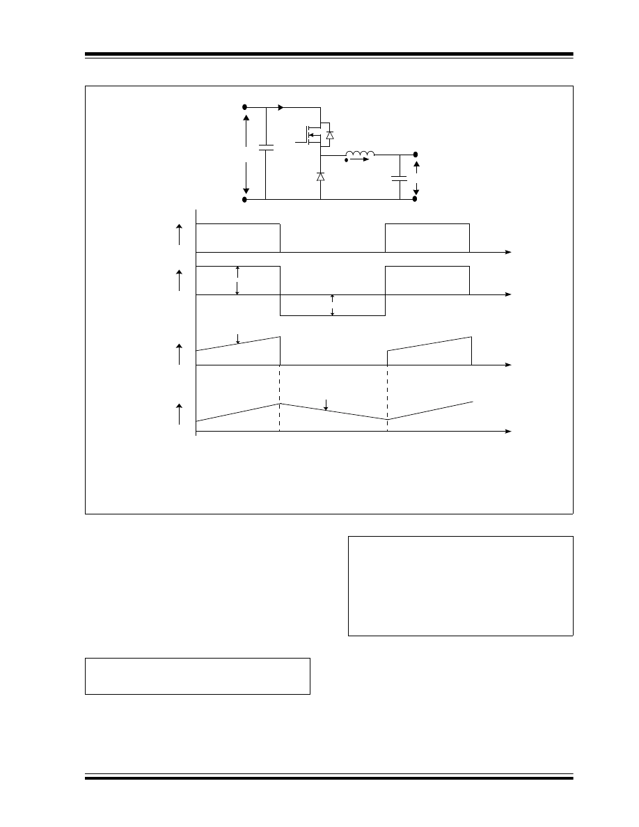
waveforms of a buck converter is shown in Figure 2.
In a buck converter, a switch (Q
1
) is placed in series
with the input voltage source V
IN
. The input source V
IN
feeds the output through the switch and a low-pass
filter, implemented with an inductor and a capacitor.
In a steady state of operation, when the switch is ON for
a period of T
ON
, the input provides energy to the output
as well as to the inductor (L). During the T
ON
period, the
inductor current flows through the switch and the
difference of voltages between V
IN
and V
OUT
is applied
to the inductor in the forward direction, as shown in
Figure 2 (C). Therefore, the inductor current I
L
rises
linearly from its present value I
L1
to I
L2,
as shown in
Figure 2 (E).
During the T
OFF
period, when the switch is OFF, the
inductor current continues to flow in the same
direction, as the stored energy within the inductor
continues to supply the load current. The diode D1
completes the inductor current path during the Q
1
OFF
period (T
OFF
); thus, it is called a freewheeling diode.
During this T
OFF
period, the output voltage V
OUT
is
applied across the inductor in the reverse direction, as
shown in Figure 2 (C). Therefore, the inductor current
decreases from its present value I
L2
to I
L1,
as shown in
Figure 2 (E).
© 2007 Microchip Technology Inc.
DS01114A -page 3
AN1114
FIGURE 2:
BUCK CONVERTER
CONTINUOUS CONDUCTION MODE
The inductor current is continuous and never reaches
zero during one switching period (T
S
); therefore, this
mode of operation is known as Continuous Conduction
mode. In Continuous Conduction mode, the relation
between the output and input voltage is given by
Equation 3, where D is known as the duty cycle, which
is given by Equation 4.
EQUATION 3:
BUCK CONVERTER V
OUT
/V
IN
RELATIONSHIP
EQUATION 4:
DUTY CYCLE
If the output to input voltage ratio is less than 0.1, it is
always advisable to go for a two-stage buck converter,
which means to step down the voltage in two buck
operations. Although the buck converter can be either
continuous or discontinuous, its input current is always
discontinuous, as shown in Figure 2 (D). This results in
a larger electromagnetic interference (EMI) filter than
the other topologies.
Q
1GATE
V
L
V
IN
-
V
OUT
-
V
OUT
-
V
OUT
/L
I
IN
I
L
(
V
IN
-
V
OUT
)/L
t
t
t
t
(B)
(C)
(D)
(E)
(A) = Buck converter
(B) = Gate pulse of MOSFET Q
1
(C) = Voltage across the Inductor L
(D) = Input current I
IN
(E) = Inductor current I
L
I
L1
I
L2
V
OUT
Q
1
D
1
I
IN
(A)
L
+
-
I
L
I
OUT
V
IN
V
OUT
D V
IN
⋅
=
where:
T
ON
= ON Period
T
S
= Switching Period
D
T
ON
T
S
----------
=

AN1114
DS01114A -page 4
© 2007 Microchip Technology Inc.
CURRENT MODE CONTROL
While designing a buck converter, there is always a
trade-off between the inductor and the capacitor size
selection.
A larger inductor value means numerous turns to the
magnetic core, but less ripple current (<10% of full load
current) is seen by the output capacitor; therefore, the
loss in the inductor increases. Also, less ripple current
makes current mode control almost impossible to
implement (refer to “Method of Control” for details on
current mode control techniques). Therefore, poor load
transient response can be observed in the converter.
A smaller inductor value increases ripple current. This
makes implementation of current mode control easier,
and as a result, the load transient response of the
converter improves. However, high ripple current
needs a low Equivalent Series Resistor (ESR) output
capacitor to meet the peak-to-peak output voltage
ripple requirement. Generally, to implement the current
mode control, the ripple current at the inductor should
be at least 30% of the full load current.
FEED-FORWARD CONTROL
In a buck converter, the effect of input voltage variation
on the output voltage can be minimized by
implementing input voltage feed-forward control. It is
easy to implement feed-forward control when using a
digital controller with input voltage sense, compared to
using an analog control method. In the feed-forward
control method, the digital controller starts taking the
appropriate adaptive action as soon as any change is
detected in the input voltage, before the change in input
can actually affect the output parameters.
SYNCHRONOUS BUCK CONVERTER
When the output current requirement is high, the
excessive power loss inside the freewheeling diode D1,
limits the minimum output voltage that can be
achieved. To reduce the loss at high current and to
achieve lower output voltage, the freewheeling diode is
replaced by a MOSFET with a very low ON state
resistance R
DSON
. This MOSFET is turned on and off
synchronously with the buck MOSFET. Therefore, this
topology is known as a synchronous buck converter. A
gate drive signal, which is the complement of the buck
switch gate drive signal, is required for this
synchronous MOSFET.
A MOSFET can conduct in either direction; which
means the synchronous MOSFET should be turned off
immediately if the current in the inductor reaches zero
because of a light load. Otherwise, the direction of the
inductor current will reverse (after reaching zero)
because of the output LC resonance. In such a
scenario, the synchronous MOSFET acts as a load to
the output capacitor, and dissipates energy in the
R
DSON
(ON state resistance) of the MOSFET, resulting
in an increase in power loss during discontinuous mode
of operation (inductor current reaches zero in one
switching cycle). This may happen if the buck converter
inductor is designed for a medium load, but needs to
operate at no load and/or a light load. In this case, the
output voltage may fall below the regulation limit, if the
synchronous MOSFET is not switched off immediately
after the inductor reaches zero.
MULTIPHASE SYNCHRONOUS BUCK
CONVERTER
It is almost impractical to design a single synchronous
buck converter to deliver more than 35 amps load
current at a low output voltage. If the load current
requirement is more than 35-40 amps, more than one
converter is connected in parallel to deliver the load.
To optimize the input and output capacitors, all the
parallel converters operate on the same time base and
each converter starts switching after a fixed time/phase
from the previous one. This type of converter is called
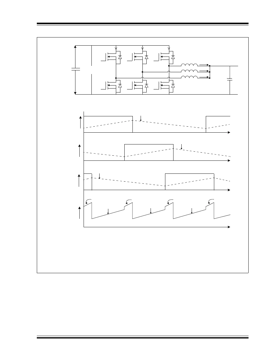
a multiphase synchronous buck converter. Figure 3
shows the multiphase synchronous buck converter
with a gate pulse timing relation of each leg and the
input current drawn by the converter. The fixed
time/phase is given by Time period/n or 300/n, where “n”
is the number of the converter connected in parallel.
The design of input and output capacitors is based on
the switching frequency of each converter multiplied by
the number of parallel converters. The ripple current
seen by the output capacitor reduces by “n” times. As
shown in Figure 3 (E), the input current drawn by a
multiphase synchronous buck converter is continuous
with less ripple current as compared to a single
converter shown in Figure 2 (D). Therefore, a smaller
input capacitor meets the design requirement in case of
a multiphase synchronous buck converter.
© 2007 Microchip Technology Inc.
DS01114A -page 5
AN1114
FIGURE 3:
MULTIPHASE SYNCHRONOUS BUCK CONVERTER
C
IN
+
-
Q
1
IQ
1
Q
2
Q
3
IQ
3
Q
4
Q
5
Q
6
I
L3
L
3
L
2
L
1
Q
1PWM
I
IN
IQ
5
+ IQ
1
IQ
1
IQ
3
IQ
5
Q
3PWM
Q
5PWM
IQ
1
+ IQ
3
IQ
3
+ IQ
5
IQ
5
+ IQ
1
t
t
t
t
(A) = Multiphase Synchronous Buck converter
(B) = Gate pulse of Q
1
, inductor current I
L1
(C) = Gate pulse of Q
3
, Inductor current I
L2
(D) = Gate pulse of Q
5
, Inductor current I
L3
(E) = Input current I
IN
IQ
5
I
L2
I
L1
I
L1
I
L2
I
L3
(A)
(B)
(C)
(D)
(E)
V
IN
V
OUT
C
O
AN1114
DS01114A -page 6
© 2007 Microchip Technology Inc.
Boost Converter
A boost converter, as its name implies, can only
produce a higher output average voltage than the input
voltage. The basic schematic with the switching
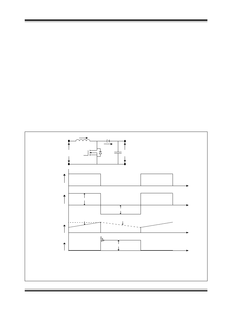
waveform of a boost converter is shown in Figure 4.
In a boost converter, an inductor (L) is placed in series
with the input voltage source V
IN
. The input source
feeds the output through the inductor and the diode D
1
.
In the steady state of operation, when the switch Q
1
is
ON for a period of T
ON
, the input provides energy to the
inductor.
During the T
ON
period, inductor current (I
L
) flows
through the switch and the input voltage V
IN
is applied
to the inductor in the forward direction, as shown in
Figure 4 (C). Therefore, the inductor current rises
linearly from its present value I
L1
to I
L2,
as shown in
Figure 4 (D). During this T
ON
period, the output load
current I
OUT
is supplied from the output capacitor C
O
.
The output capacitor value should be large enough to
supply the load current for the time period T
ON
with the
minimum specified droop in the output voltage.
During the T
OFF
period when the switch is OFF, the
inductor current continues to flow in the same direction
as the stored energy with the inductor, and the input
source V
IN
supplies energy to the load. The diode D
1
completes the inductor current path through the output
capacitor during the Q
1
OFF period (T
OFF
). During this
T
OFF
period, the inductor current flows through the
diode and the difference of voltages between V
IN
and
V
OUT
is applied to the inductor in the reverse direction,
as shown in Figure 4 (C). Therefore, the inductor
current decreases from the present value I
L2
to I
L1,
as
CONTINUOUS CONDUCTION MODE
As shown in Figure 4 (D), the inductor current is
continuous and never reaches zero during one switching
cycle (T
S
); therefore, this method is known as
Continuous Conduction mode, which is the relation
between output and input voltage, as shown in
Equation 5.
FIGURE 4:
BOOST CONVERTER
V
OUT
+
-
+
-
Q
1
V
IN
+
-
I
L
V
L
D
1
I
D1
Q
1PWM
V
L
IQ
1
I
D1
V
IN
V
OUT
- V
IN
V
OUT
I
L2
V
DS
t
t
t
t
I
OUT
(A)
(B)
(C)
(D)
(E)
(A) = Boost converter
(B) = Gate pulse of MOSFET Q
1
(C) = Voltage across the inductor L
(D) = Current through the MOSFET Q
1
and diode D
1
(E) = Voltage across the MOSFET Q
1
I
L1
C
O
© 2007 Microchip Technology Inc.
DS01114A -page 7
AN1114
EQUATION 5:
V
OUT
/V
IN
RELATIONSHIP
The root mean square (RMS) ripple current in the
output capacitor is given by Equation 6. It is calculated
by considering the waveform shown in Figure 4 (D).
During the T
OFF
period, the pulsating current I
D1,
flows
into the output capacitor and the constant load current
(I
OUT
) flows out of the output capacitor.
EQUATION 6:
CAPACITOR RIPPLE RMS
CURRENT
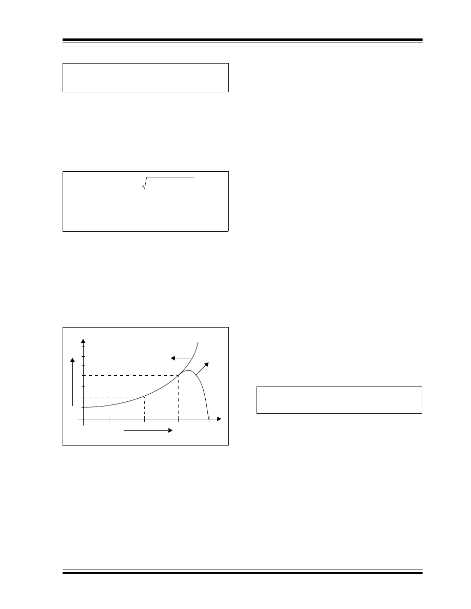
Based on Equation 5, the V
OUT
/V
IN
ratio can be very
large when the duty cycle approaches unity, which is
ideal. However, unlike the ideal characteristic,
V
OUT
/V
IN
declines as the duty ratio approaches unity,
as shown in Figure 5. Because of very poor utilization
of the switch, parasitic elements occur in the
components and losses associated with the inductor
capacitor and semiconductors.
FIGURE 5:
V
OUT
/V
IN
AND DUTY CYCLE
IN BOOST CONVERTER
POWER FACTOR CORRECTION
When the boost converter operates in Continuous
Conduction mode, the current drawn from the input
voltage source is always continuous and smooth, as
shown in Figure 4 (D). This feature makes the boost
converter an ideal choice for the Power Factor
Correction (PFC) application. Power Factor (PF) is
given by the product of the Total Current Harmonics
Distortion Factor (THD) and the Displacement Factor
(DF). Therefore, in PFC, the input current drawn by the
converter should be continuous and smooth enough to
meet the THD of the input current so that it is close to
unity. In addition, input current should follow the input
sinusoidal voltage waveform to meet the displacement
factor so that it is close to unity.
Forward Converter
A forward converter is a transformer-isolated converter
based on the basic buck converter topology. The basic
schematic and switching waveforms are shown in
Figure 6.
In a forward converter, a switch (Q
1
) is connected in
series with the transformer (T
1
) primary. The switch
creates a pulsating voltage at the transformer primary
winding. The transformer is used to step down the
primary voltage, and provide isolation between the
input voltage source V
IN
and the output voltage V
OUT
.
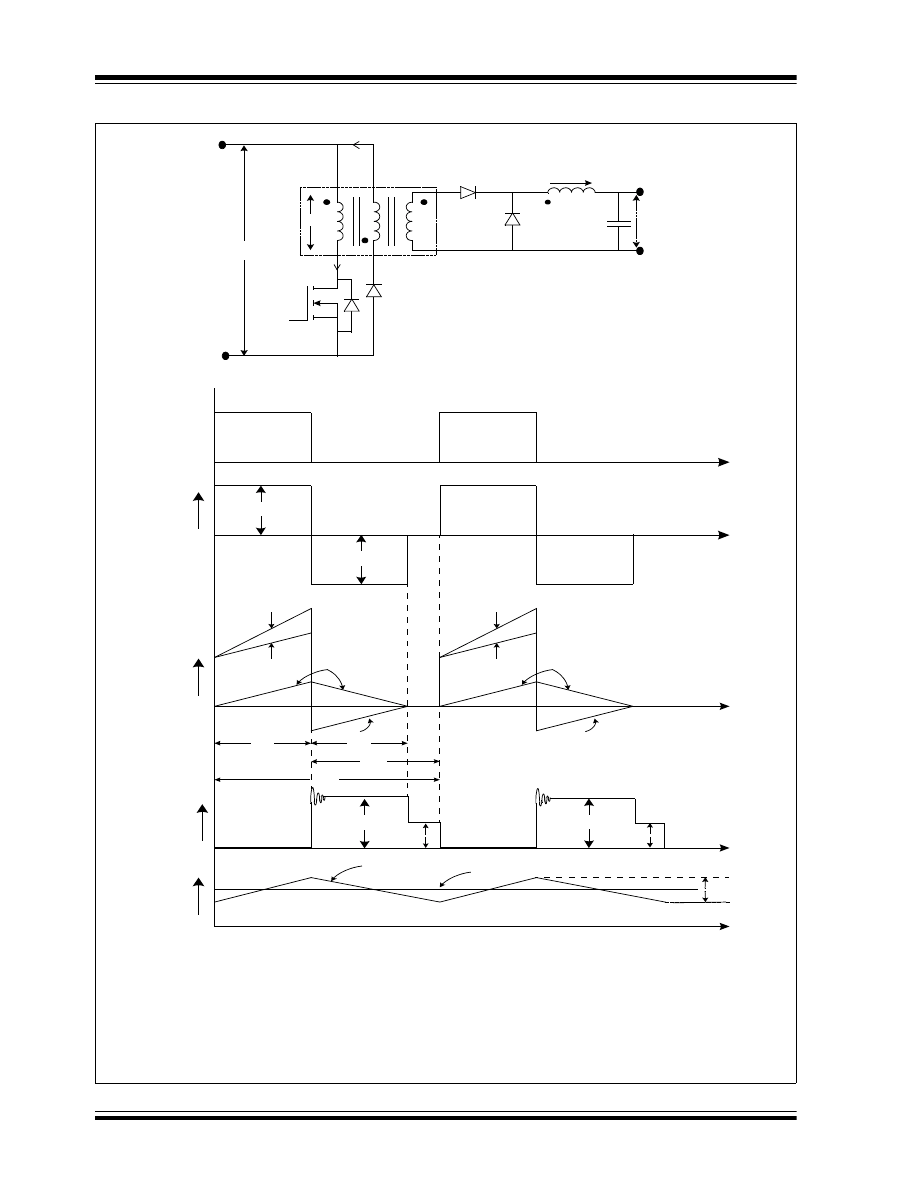
In the steady state of operation, when the switch is ON
for a period of T
ON
, the dot end of the winding becomes
positive with respect to the non-dot end. Therefore, the
diode D
1
becomes forward-biased and the diodes D
2
and D
3
become reverse-biased.
As the input voltage V
IN
is applied across the
transformer primary, the magnetizing current I
M
increases linearly from its initial zero value to a final
value with a slope of V
IN
/L
M
, where L
M
is the
magnetizing inductance of the primary winding, as
shown in Figure 6(D). The total current that flows
through the primary winding is this magnetizing current
plus the inductor current (I
L
) reflected on the primary
side. This total current flows through the MOSFET
during the T
ON
period. The voltage across the diode D
2
is equal to the input voltage multiplied by the
transformer turns ratio (N
S
/N
P
). In the case of a forward
converter, the voltage applied across the inductor L in
the forward direction during the T
ON
period, is given by
Equation 7, neglecting the transformer losses and the
diode forward voltage drop.
EQUATION 7:
FORWARD VOLTAGE
ACROSS INDUCTOR
DISSIPATING ENERGY
At the end of the ON period, when the switch is turned
OFF, there is no current path to dissipate the stored
energy in the magnetic core. There are many ways to
dissipate this energy. One such method is shown in
Figure 6. In this method, the flux stored inside the
magnetic core induces a negative voltage at the dot
end of the N
R
winding, which forward biases the diode
D
3
and resets the magnetizing energy stored in the
core. Therefore, the N
R
winding is called the reset
winding. Resetting the magnetizing current during the
OFF period is important to avoid saturation.
During the T
OFF
period when the switch is OFF, the
inductor current (I
L
) continues to flow in the same
direction, while the stored energy within the inductor
continues to supply the load current I
OUT
.
V
OUT
V
IN
1 D
–
(
)
------------------
=
I
RIPPLERMS
I
D1
(
)
2
I
OUT
(
)
2
–
=
where:
I
D1RMS
= RMS value of I
D1
I
RIPPLERMS
= Ripple RMS current of capacitor
I
OUT
= Output DC current
1
2
3
4
5
6
7
Ideal
0.25
0.5
0.75
1
Practical
Duty Cycle = D
V
OUT
/V
IN
V
L
V
IN
N
S
N
P
------- V
OUT
–
⋅
L
I
L
Δ
t
Δ
--------
⋅
=
=
AN1114
DS01114A -page 8
© 2007 Microchip Technology Inc.
FIGURE 6:
FORWARD CONVERTER
V
IN
N
P
N
S
Q
1
D
1
D
2
+
-
+
-
G
S
D
+
-
I
SW
N
R
I
3
T
1
D
3
+
-
V
P
I
L
V
L
Q
1PWM
V
P
I
M
I
P
I
M
V
IN
V
IN
T
ON
T
M
T
OFF
T
S
I
L
I
OUT
I
IN
V
DS
I
L
I
M
I
P
I
M
I
3
I
3
V
IN
ΔI
L
(A)
(B)
(C)
(D)
(E)
(F)
(A) = Forward Converter power circuit diagram.
(B) = Gate pulse of MOSFET Q
1
(C) = Voltage across the transformer primary winding N
P
(D) = Current through N
P
and N
R
(E) = Voltage across the MOSFET Q
1
(F) = Output Inductor current I
L
t
t
t
t
t
V
OUT
(1+N
P
/N
R
) • V
IN
(1+N
P
/N
R
) • V
IN
(1+N
P
/N
R
) • V
IN

© 2007 Microchip Technology Inc.
DS01114A -page 9
AN1114
The diode D
2
, called a freewheeling diode, completes
the inductor current path during the Q
1
off period
(T
OFF
). During this T
OFF
period, the output voltage V
OUT
is applied across the inductor in the reverse direction.
In a continuous conduction mode of operation, the rela-
tion between the output voltage and input voltage is
given by Equation 8, where D is the duty cycle.
EQUATION 8:
FORWARD CONVERTER
V
OUT
/V
IN
RELATIONSHIP
CONTROLLING MAGNETIZATION
When the switch is turned OFF, the diode D
1
becomes
reverse-biased, and I
M
cannot flow in the secondary
side. Therefore, the magnetizing current is taken away
by the reset winding of the transformer, as shown in
Figure 6(A and D).
The reflected magnetizing current I
3
flows through the
reset winding N
R
and the diode D
3
into the input supply.
During the interval T
M
when I
3
is flowing, the voltage
across the transformer primary as well as L
M
is given
EQUATION 9:
REFLECTED VOLTAGE AT
PRIMARY
Time taken by the transformer to complete the
demagnetization can be obtained by recognizing that
the time integral of voltage across the L
M
must be zero
over one time period. The maximum value of T
M
, as
shown in Figure 6, is the time it takes the transformer
to completely demagnetize before the next cycle
begins and is equal to T
OFF
. Therefore, the maximum
duty cycle and the maximum drain-to-source blocking
voltage (V
DS
) seen by the switch (Q
1)
in a forward
converter having number of primary and number of
reset winding turns as N
P
and N
R
, is given by
EQUATION 10: MAXIMUM DUTY CYCLE
AND V
DS
The maximum value of T
M
/T
S
to completely
demagnetize before the next cycle begins is equal to
(1-D), so the maximum duty ratio for the forward
converter is given by Equation 10.
From Equation 10, it is understood that when the
number of primary winding turns, N
P
, is equal to the
number of the reset winding turns, N
R
, the switch can
have a maximum 50% duty cycle and the blocking
voltage of the switch will be equal to twice the input
voltage. The practical limit of maximum duty cycle
should be 45%, and maximum blocking voltage seen
by the switch will be more than twice the input voltage
due to the nonlinearity of components and the leakage
inductance of the transformer.
EQUATION 11: MAGNETIZING STORED
ENERGY IN FLYBACK
TRANSFORMER
If N
R
is chosen to be less than N
P
, the maximum duty
cycle D
MAX
can be more than 50%; however, the
maximum blocking voltage stress of the switch
becomes more than 2 • V
IN
the value of D
MAX
and V
DS
,
as shown in Equation 10. If N
R
is chosen to be larger
than N
P
, D
MAX
will be less than 50%, but the maximum
blocking voltage stress of the switch is now less than
2 • V
IN,
the value of D
MAX
and V
DS
, as shown in
Equation 10.
Since large voltage isolation is not required between
the reset and the primary windings, these two windings
can be wound bifilar to minimize leakage inductance.
The reset winding carries only the magnetizing current,
which means it requires a smaller size of wire as
compared to the primary winding.
V
IN
N
S
N
P
------- V
OUT
–
⋅
⎝
⎠
⎛
⎞ T
ON
V
OUT
T
OFF
⋅
=
⋅
V
OUT
V
IN
N
S
N
P
-------
⎝
⎠
⎛
⎞ D
⋅
⋅
=
N
P
N
R
-------
⎝
⎠
⎛
⎞ V
IN
⋅
1 D
MAX
–
(
)
N
R
N
P
-------
⎝
⎠
⎛
⎞ D
MAX
⋅
=
D
MAX
1
1
N
R
N
P
-------
⎝
⎠
⎛
⎞
+
⎝
⎠
⎛
⎞
---------------------------
=
V
DS
V
IN
V
IN
N
P
N
R
-------
⎝
⎠
⎛
⎞
⋅
+
=
E
P
= Joules
I
PK
= Amps
L
M
= Henries
where:
E
P
1
2
---
I
PK
(
)
2
L
M
⋅
⋅
=
I
PK
V
IN
T
ON
⋅
(
)
L
M
----------------------------
=
AN1114
DS01114A -page 10
© 2007 Microchip Technology Inc.
To demagnetize the transformer core, a Zener diode or
R
C
snubber circuit can also be used across the
transformer instead of the transformer reset winding.
The incomplete utilization of the magnetics, the
maximum duty cycle limit and the high voltage stress of
the switch, make a forward converter feasible for the
output power (up to 150 watts) of an off-line low-cost
power supply. Its non-pulsating output inductor current
makes the forward converter well suited for the
application involving a very high load current (>15A).
The presence of the output inductor limits the use of a
forward converter in a high output voltage (>30V)
application, which requires a bulky inductor to oppose
the high output voltage.
INCREASING EFFICIENCY
The efficiency of a forward converter is low compared
to other topologies with the same output power, due to
the presence of four major loss elements: the switch,
transformer, output diode rectifiers and output inductor.
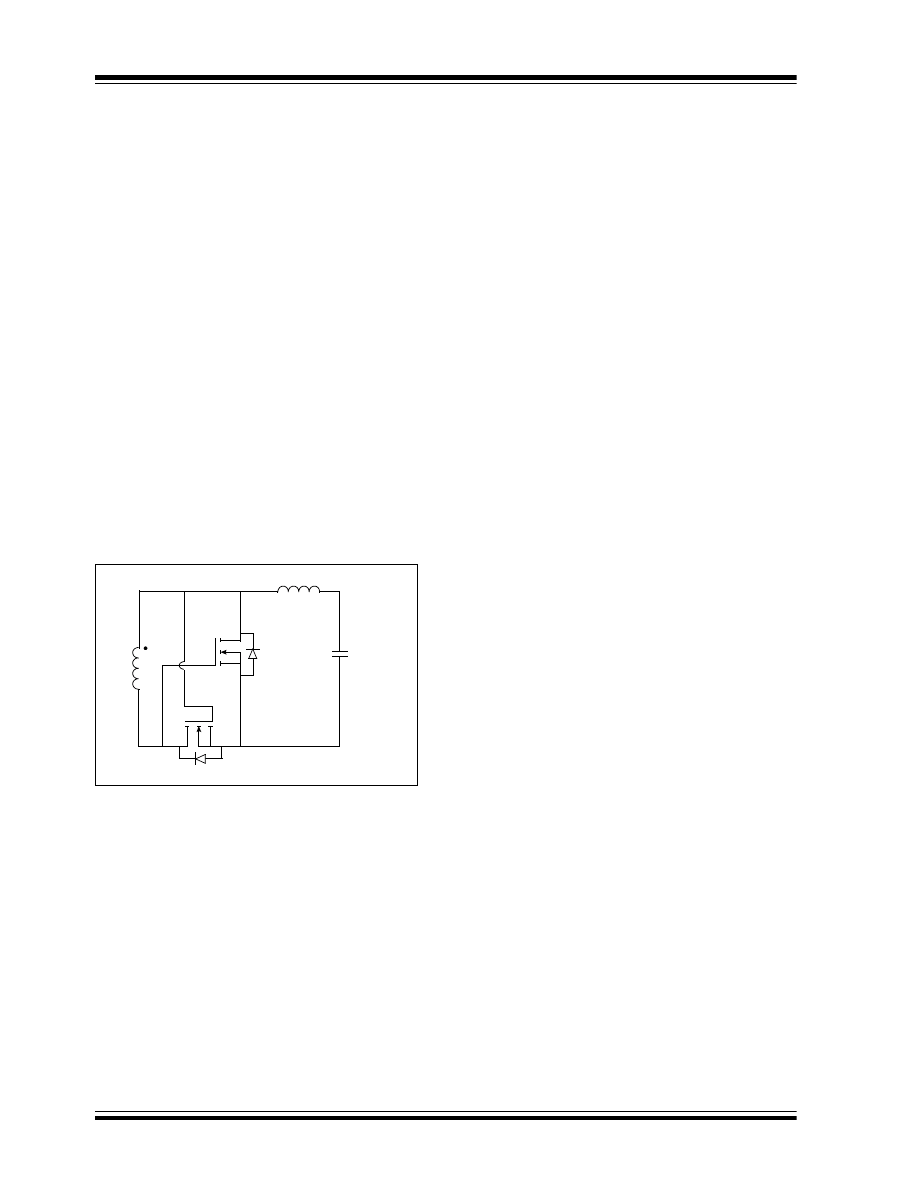
To increase efficiency, a synchronous MOSFET can be
used in place of the output diode rectifier. The
MOSFET can be self-driven through the extra or the
same windings in the transformer secondary, as shown
in Figure 7.
FIGURE 7:
SYNCHRONOUS RECTIFIER
Improving the load transient response and
implementing current mode control requires reducing
the output inductor value and the use of a better output
capacitor to meet the output voltage ripple requirement,
as discussed in the “Buck Converter” section. A
multiple output, forward converter coupled inductor is
used to get better cross-load regulation requirements.
Two-Switch Forward Converter
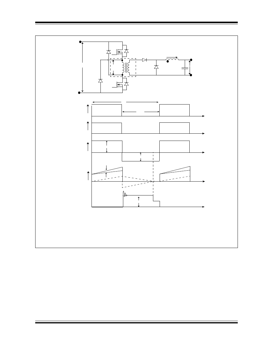
The maximum voltage stress of the switch in a forward
converter can be limited to a value equal to the input
voltage, by placing one more switch (Q
2)
in series with
the transformer primary winding, as shown in Figure 8.
The resulting converter is called a two-switch forward
converter. The basic schematic and switching
waveforms of the two-switch forward converter are
shown in Figure 8.
The switches Q
1
and Q
2
are controlled by the same
gate drive signal, as shown in Figure 8 (B and C). In the
steady state of operation, when the switches Q
1
and Q
2
are ON for a T
ON
period, the input voltage V
IN
is applied
to the transformer primary. During the T
ON
period, the
magnetizing current plus the reflected output inductor
current flows through the transformer primary and the
switches Q
1
and Q
2
.
At the end of the ON period, when the switches are
turned OFF, the flux stored inside the magnetic core
induces a voltage in the reverse direction to the
transformer primary winding, which forward-biases the
diodes D
1
and D
2,
and provides a path to the
magnetizing current to reset the core. The voltage V
IN
is applied across the transformer primary winding in the
reverse direction, as shown in Figure 8 (D). If there is
no leakage inductance in the transformer T
1
, the
voltage across N
P
would be equal to V
IN
, and the
maximum blocking voltage across the switch is V
IN
.
When the magnetizing current reaches zero, diodes D
1
and D
2
become reverse-biased and remain zero for the
rest of the switching period. The secondary side
operation of the two-switch forward converter is the
same as the operation of the forward converter
explained earlier.
APPLICATION CONSIDERATIONS
Reduction in the blocking voltage of the switch allows
the designer to select a better low-voltage MOSFET for
the design. Therefore, the two-switch forward
converter can be used up to the output power level of
350 watts. If peak current is greater than 350 watts,
losses across the MOSFET become impractical to
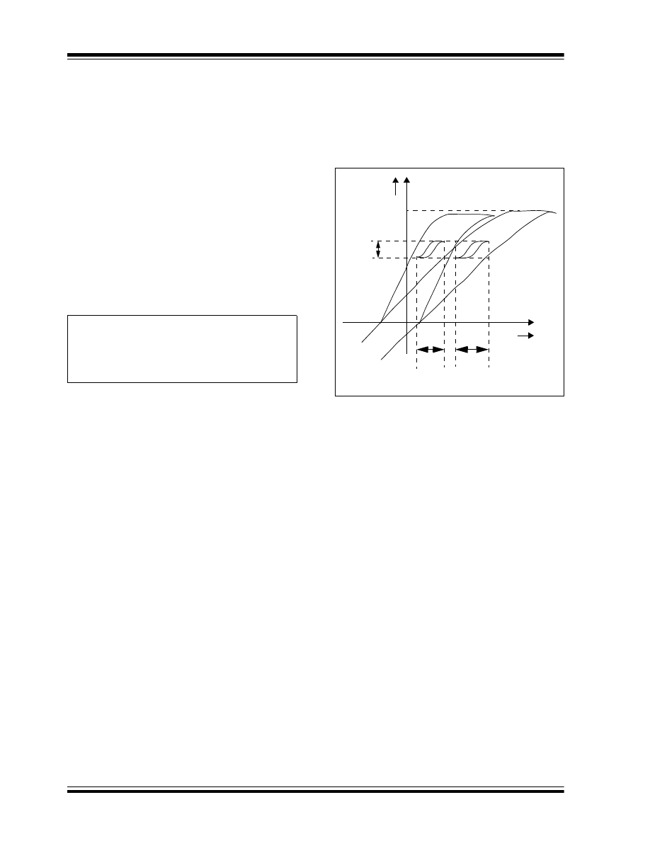
handle, and incomplete utilization of magnetic makes
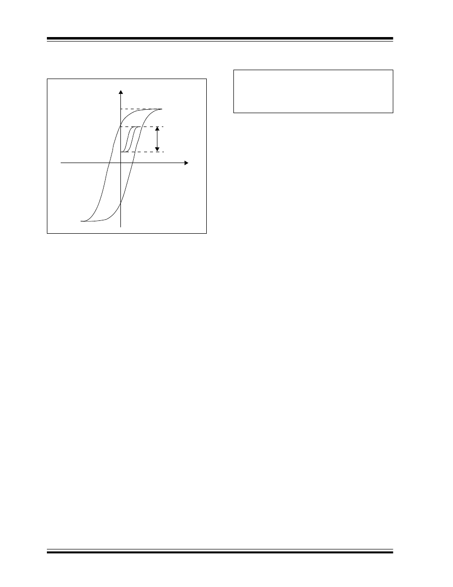
the transformer bulky (see Figure 9). Therefore, the
two-switch forward converter is best suited for
applications with an output power level range of 150 to
350 watts.
Q
1
G
S
D
D
S
G
Q
2
© 2007 Microchip Technology Inc.
DS01114A -page 11
AN1114
FIGURE 8:
TWO-SWITCH FORWARD CONVERTER
.
Q
1PWM
V
P
V
IN
Q
2PWM
T
S
T
OFF
V
IN
N
P
N
S
Q
1
D
3
D
4
+
-
+
-
D
+
-
V
P
I
L
V
L
Q
2
D
D
1
D
2
V
P
V
IN
V
IN
I
N
I
P
(A)
(A) = Two-switch forward converter power circuit
(B) = Gate pulse for MOSFET Q
1
(C) = Gate pulse for MOSFET Q
2
(D) = Voltage across the primary winding N
P
(E) = Current through the primary winding N
P
(F) = Voltage across the MOSFET Q
1
and Q
2
(B)
(C)
(D)
(E)
(F)
t
t
t
t
t
V
OUT
AN1114
DS01114A -page 12
© 2007 Microchip Technology Inc.
FIGURE 9:
TRANSFORMER BH CURVE
OF SINGLE SWITCH
CONVERTER
Flyback Converter (FBT)
A flyback converter (FBT) is a transformer-isolated
converter based on the basic buck boost topology. The
basic schematic and switching waveforms are shown in
Figure 10.
In a flyback converter, a switch (Q
1
) is connected in
series with the transformer (T
1
) primary. The
transformer is used to store the energy during the ON
period of the switch, and provides isolation between the
input voltage source V
IN
and the output voltage V
OUT
.
In a steady state of operation, when the switch is ON for
a period of T
ON
, the dot end of the winding becomes
positive with respect to the non-dot end. During the T
ON
period, the diode D
1
becomes reverse-biased and the
transformer behaves as an inductor. The value of this
inductor is equal to the transformer primary
magnetizing inductance L
M
, and the stored
magnetizing energy (see Equation 11) from the input
voltage source V
IN
. Therefore, the current in the
primary transformer (magnetizing current I
M
) rises
linearly from its initial value I
1
to I
PK
, as shown in
Figure 10 (D).
As the diode D1 becomes reverse-biased, the load
current (I
OUT
) is supplied from the output capacitor
(C
O
). The output capacitor value should be large
enough to supply the load current for the time period
T
ON
, with the maximum specified droop in the output
voltage.
EQUATION 12: FLYBACK CONVERTER
V
OUT
/V
IN
RELATIONSHIP
At the end of the T
ON
period, when the switch is turned
OFF, the transformer magnetizing current continues to
flow in the same direction. The magnetizing current
induces negative voltage in the dot end of the
transformer winding with respect to non-dot end. The
diode D
1
becomes forward-biased and clamps the
transformer secondary voltage equal to the output
voltage.
The energy stored in the primary of the flyback
transformer transfers to secondary through the flyback
action. This stored energy provides energy to the load,
and charges the output capacitor. Since the
magnetizing current in the transformer cannot change
instantaneously at the instant the switch is turned OFF,
the primary current transfers to the secondary, and the
amplitude of the secondary current will be the product
of the primary current and the transformer turns ratio,
N
P
/N
S
.
DISSIPATING STORED LEAKAGE ENERGY
At the end of the ON period, when the switch is turned
OFF, there is no current path to dissipate the stored
leakage energy in the magnetic core of the flyback
transformer. There are many ways to dissipate this
leakage energy. One such method is shown in
Figure 10 as a snubber circuit consisting of D
2
, R
S
and
C
S
. In this method, the leakage flux stored inside the
magnetic core induces a positive voltage at the non-dot
end primary winding, which forward-biases the diode
D
2
and provides the path to the leakage energy stored
in the core, and clamps the primary winding voltage to
a safe value. During this process, C
S
is charged to a
voltage slightly more than the reflected secondary
flyback voltage, which is known as flyback overshoot.
The spare flyback energy is dissipated in resistor R
S
. In
a steady state, and if all other conditions remain
constant, the clamp voltage is directly proportional to
R
S
. The flyback overshoot provides additional forcing
volts to drive current into the secondary leakage
inductance during the flyback action. This results in a
faster increase in the transformer secondary current,
which improves the efficiency of the flyback
transformer.
CONTINUOUS CONDUCTION MODE
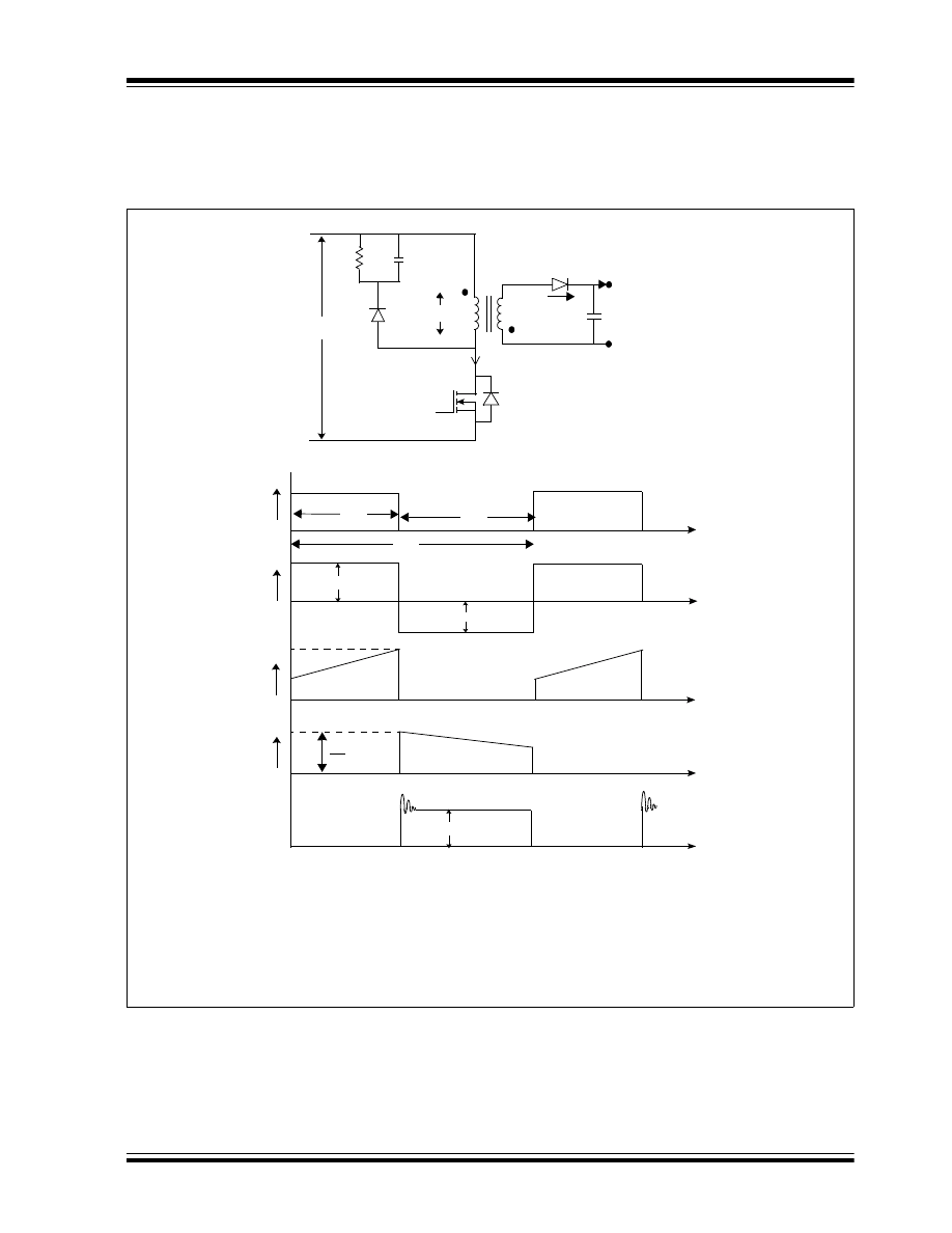
The waveform shown in Figure 10 (D) represents
Continuous Conduction mode operation of a flyback
converter. Continuous Conduction mode corresponds
to the incomplete demagnetization of the flyback
transformer core. The core flux increases linearly from
ΔB
B
H
B
SAT
V
OUT
V
IN
-------------
N
S
N
P
-------
⎝
⎠
⎛
⎞
D
1 D
–
(
)
------------------
⎝
⎠
⎛
⎞
⋅
=
where:
D = the duty cycle of the flyback switch
© 2007 Microchip Technology Inc.
DS01114A -page 13
AN1114
the initial value flux (0) to flux (P
K
) during the ON
period, T
ON
. In a steady state, the change in core flux
during the T
ON
period should be equal to the change in
flux during the T
OFF
period. This is important to avoid
saturation. The relation between the input and output
voltage in a steady state and continuous mode of
operation is given by Equation 12.
FIGURE 10:
FLYBACK CONVERTER
Q
1PWM
I
D1
V
P
V
IN
N
P
N
S
Q
1
D
1
+
-
D
V
P
D
2
V
CLAMP
R
S
C
S
I
D1
V
IN
I
SW
N
P
N
S
T
S
T
ON
T
OFF
(A) = Flyback converter power circuit
(B) = Gate pulse for the MOSFET Q
1
(C) = Voltage across the primary winding
(D) = Current through MOSFET Q
1
(E) = Current through the diode D
1
(F) = Voltage across the MOSFET Q
1
(A)
(B)
(C)
(D)
(E)
(F)
t
t
t
t
t
I
SW
I
1
I
PK
V
OUT
I
OUT
V
IN
+ V
CLAMP
•
I
PK
AN1114
DS01114A -page 14
© 2007 Microchip Technology Inc.
During Continuous Conduction mode of operation, the
duty cycle is independent of the load drawn from the
converter, and is a constant for the DC input voltage.
However, in a practical situation the load increases the
loss inside the transformer and the output diode D
2
loss
is also increased. To maintain constant output voltage,
the duty cycle varies slightly in Continuous Conduction
mode at a constant DC input voltage.
Because of the presence of the secondary reflected
voltage on the primary winding and the leakage stored
energy in the transformer core, the maximum voltage
stress V
DS
of the switch is given by Equation 13. If the
flyback converter is used for universal input of the
off-line power supply, the switch voltage rating should
be 700V, considering the secondary reflected voltage
of 180V and 20% volts of leakage spike due to leakage
energy storage in the transformer.
EQUATION 13: MAXIMUM V
DS
IN FLYBACK
CONVERTER
SELECTING A CAPACITOR
The pulsating current I
D1,
as shown in Figure 10(E),
flows in, and the DC load current flows out of the output
capacitor, which causes the output capacitor of the
flyback converter to be highly stressed. In the flyback
converter, the selection of the output capacitor is based
on the maximum ripple RMS current seen by the
capacitor given by Equation 6, and the maximum
peak-to-peak output voltage ripple requirements. The
output voltage peak-to-peak ripple depends on the
ripple current seen in the capacitor and its Equivalent
Series Resistor (ESR). The ESR of the capacitor and
the ripple current cause heating inside the capacitor,
which affects its predictive life. Therefore, selection of
the capacitor depends highly on the ripple current
rating and the ESR value so as to meet the
temperature rise and output voltage ripple requirement.
If the output ripple current is high, it is advisable to have
more than one capacitor in parallel in place of a single,
large capacitor. These capacitors should be placed at
an equal distance from the diode cathode terminal, so
that each capacitor shares equal current.
AIR GAP
To increase the throughput capability and reduce the
chances of magnetic saturation in the flyback
transformer core, an air gap is inserted in the limb of the
transformer core. This air gap doesn't change the
saturation flux density (B
SAT
) value of the core
material; however, it increases the magnetic field
intensity, H, to reach saturation and reduces the
residual flux density, B
R
, as shown in Figure 11.
Therefore, the air gap increases the working range of
delta BH to increase the throughput of the flyback
transformer.
FIGURE 11:
BH CURVE WITH AIR GAP
FOR THE FLYBACK
TRANSFORMER
ADVANTAGES OF FLYBACK TOPOLOGY
Flyback topology is widely used for the output power
from a maximum of a 5 to150 watt low-cost power
supply. Flyback topology doesn’t use an output
inductor, thus saving cost and volume as well as losses
inside the flyback converter. It is best suited for
delivering a high output voltage up to 400V at a low
output power up to 15-20 watts. The absence of the
output inductor and the freewheeling diode (used in the
forward converter) makes the flyback converter
topology best suited for high output voltage
applications.
In a flyback converter, when more than one output is
present, the output voltages track one another with the
input voltage and the load changes, far better than they
do in the forward converter. This is because of the
absence of the output inductor, so the output capacitor
connects directly to the secondary of the transformer
and acts as a voltage source during the turned off
period (T
OFF
) of the switch.
APPLICATION CONSIDERATIONS
For the same output power level, and if the output
current requirement is more than 12-15 amps, the RMS
peak-to-peak ripple current seen by the output
capacitor is very large, and becomes impractical to
handle. Therefore, it is better to use the forward
converter topology than the flyback topology for an
application where the output current requirement is
high.
V
DS
V
IN
V
CLAMP
V
LEAKAGE
+
+
=
where:
V
CLAMP
= Voltage across the snubber circuit (D
2
, R
2
, and C
2
)
V
LEAKAGE
= Leakage spike voltage due to leakage energy
B
SAT
Δ
BAC
ΔH
ΔH
H
B
(air gap)
without air gap

© 2007 Microchip Technology Inc.
DS01114A -page 15
AN1114
Push-Pull Converter
A push-pull converter is a transformer-isolated
converter based on the basic forward topology. The
basic schematic and switching waveforms are shown in
Figure 12.
The high-voltage DC is switched through the
center-tapped primary of the transformer by two
switches, Q
1
and Q
2
, during alternate half cycles.
These switches create pulsating voltage at the
transformer primary winding. The transformer is used
to step down the primary voltage and to provide
isolation between the input voltage source V
IN
and the
output voltage V
OUT
.
The transformer used in a push-pull converter consists
of a center-tapped primary and a center-tapped
secondary. The switches Q
1
and Q
2
are driven by the
control circuit, such that both switches should create
equal and opposite flux in the transformer core.
AN1114
DS01114A -page 16
© 2007 Microchip Technology Inc.
In the steady state of operation, when Q
1
is ON for the
period of T
ON
, the dot end of the windings become
positive with respect to the non-dot end. The diode D
5
becomes reverse-biased and the diode D
6
becomes
forward-biased. Thus, the diode D
6
provides the path to
the output inductor current I
L
through the transformer
secondary N
S2
. As the input voltage V
IN
is applied to
the transformer primary winding N
P1
, a reflected
primary voltage appears in the transformer secondary.
The difference of voltages between the transformer
secondary and output voltage V
OUT
is applied to the
inductor L in the forward direction. Therefore, the
inductor current I
L
rises linearly from its initial value of
I
L1
to I
L2,
as shown in Figure 12(E). During this T
ON
period while the input voltage is applied across the
transformer primary N
P1
, the value of the magnetic flux
density in the core is changed from its initial value of B
1
to B
2,
as shown in Figure 13.
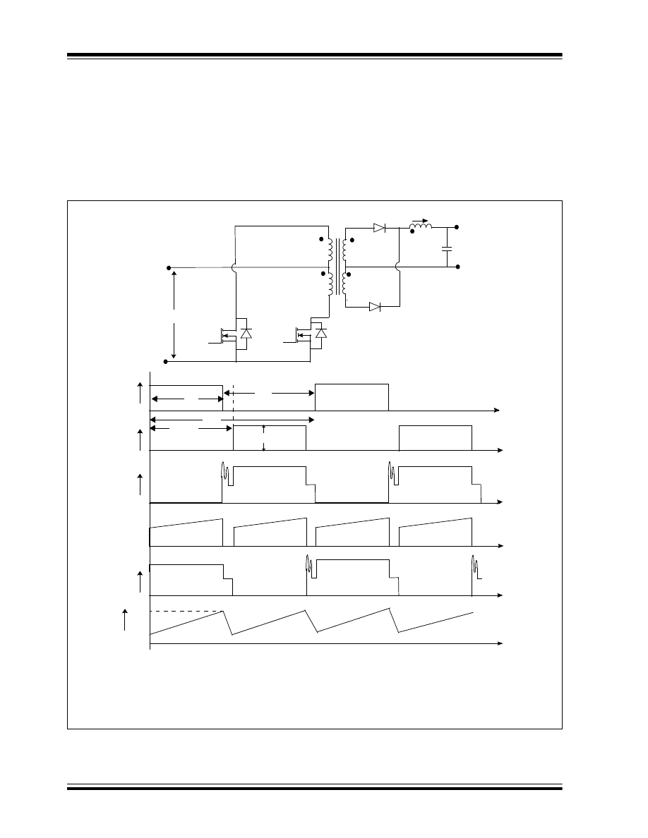
FIGURE 12:
PUSH-PULL CONVERTER
V
IN
Q
2
D
6
+
-
D
D
5
Q
1
D
N
P2
N
P1
Q
1PWM
I
IN
Q
2PWM
V
IN
V
DS2
I
L
V
DS1
IQ
1
IQ
2
IQ
1
IQ
2
t
t
t
t
t
t
N
S2
N
S1
V
OUT
I
OUT
L
+
-
I
L
I
L1
I
L2
T
ON
Ts
T
S
/2
T
OFF
(A)
(B)
(C)
(D)
(E)
(A) = Push-pull converter
(B) = Gate pulse of MOSFET Q
1
(C) = Drain-to-source voltage Vds of MOSFET Q
1
(D) = Current through the MOSFET Q
1
and Q
2
(E) = Output inductor current
© 2007 Microchip Technology Inc.
DS01114A -page 17
AN1114
At the end of the T
ON
period, the switch Q
1
is turned
OFF, and remains off for the rest of the switching period
T
S
. The switch Q
2
will be turned ON after half of the
switching period T
S
/2, as shown in Figure 12. Thus,
during the T
OFF
period, both of the switches (Q
1
and
Q
2
) are OFF. When switch Q
1
is turned OFF, the body
diode of the switch provides the path for the leakage
energy stored in the transformer primary, and the
output rectifier diode D
5
becomes forward-biased. As
the diode D
5
becomes forward-biased, it carries half of
the inductor current through the transformer secondary
N
S1,
and half of the inductor current is carried by the
diode D
6
through the transformer secondary N
S2
. This
results in equal and opposite voltages applied to the
transformer secondaries, assuming both secondary
windings N
S1
and N
S2
have an equal number of turns.
Therefore, the net voltage applied across the
secondary during the T
OFF
period is zero, which keeps
the flux density in the transformer core constant to its
final value B
2
. The output voltage V
OUT
is applied to the
inductor L in the reverse direction when both switches
are OFF. Thus, the inductor current I
L
decreases
linearly from its initial value of I
L2
to I
L1,
as shown in
AVOIDING MAGNETIC SATURATION
After the time period T
S
/2, when the switch Q
2
turns
ON, the diode D
6
become reverse-biased, and the
complete inductor current starts flowing through the
diode D
5
and transformer secondary N
S1
. During this
T
ON
period, when the switch Q
2
is turned ON, the input
voltage V
IN
is applied to the transformer primary N
P2
in
the reverse direction, which makes the dot end
negative with respect to the non-dot end.
As the input voltage applies across the transformer
primary N
P2
, the value of the magnetic flux density in
the core is changed from its initial value of B
2
to B
1,
as
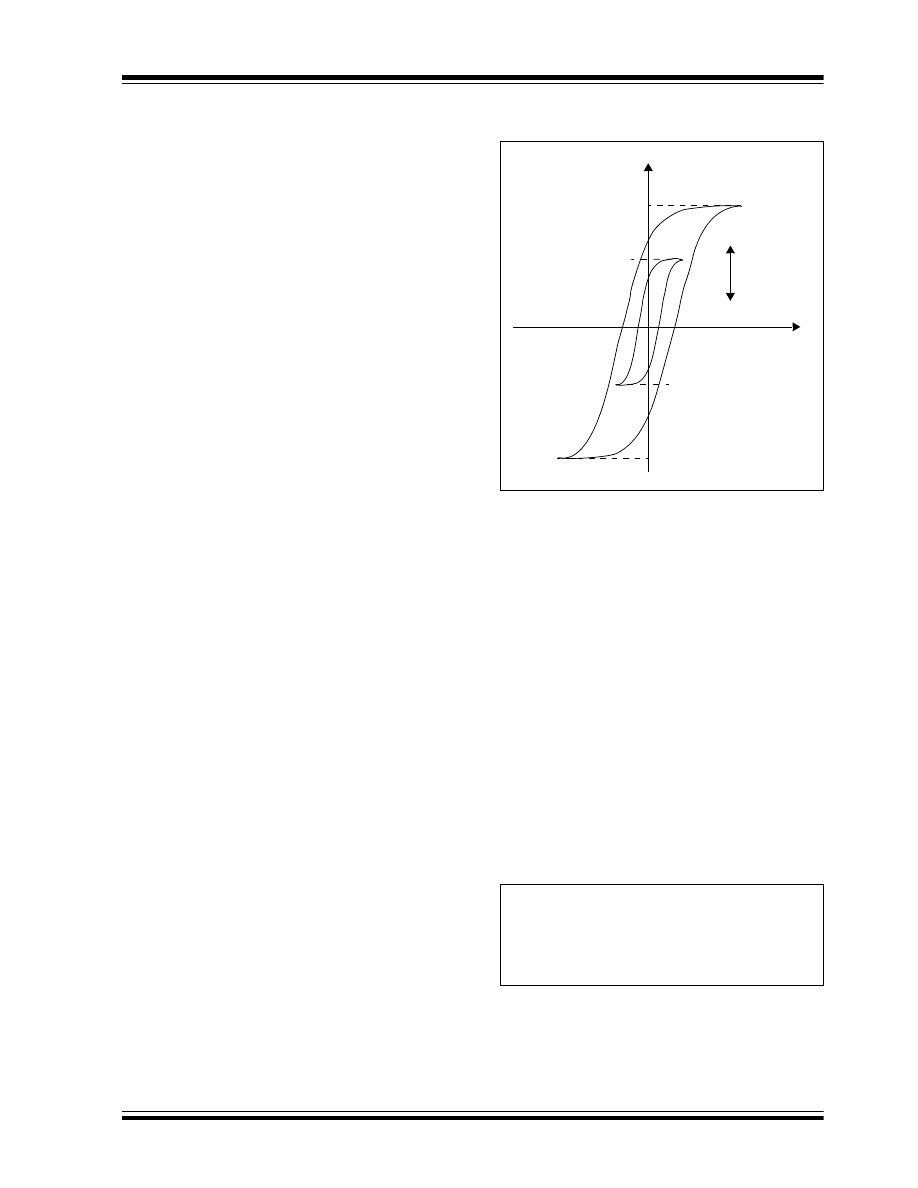
shown in Figure 13. Assuming the number of primary
turns N
P1
is equal to N
P2,
and the number of secondary
winding turns N
S1
is equal to N
S2
, the T
ON
period of
both switches should be the same to avoid magnetic
saturation in the transformer core. After the T
ON
period,
Q
2
turns OFF and remains off for the rest of the period
T
S
, as shown in Figure 12.
FIGURE 13:
BH CURVE FOR PUSH-PULL
TRANSFORMERVOLTAGE
VOLTAGE RATING OF SWITCH
During the T
ON
period of any switch, the voltage V
IN
is
applied to half of the transformer primary and induces
equal voltage to the other half of the transformer
primary winding. This results in twice the input voltage
applied to the off switch. Therefore, the switches used
for the push-pull converter must be rated at least twice
the maximum input voltage. For practical purposes, the
voltage rating of the switch should be 20% more than
the theoretical calculation due to leakage spike and
transients. For the universal input voltage, the rating of
the switch used should be: 264 • 1.414 • 2 • 1.2 = 895,
which means a 900 volt switch is required.
V
OUT
/V
IN
RELATIONSHIP
In the steady state and Continuous Conduction mode
of operation, the relation between the input and output
voltage is given by Equation 14, where D is the duty
cycle of the switch.
EQUATION 14: PUSH-PULL CONVERTER
V
OUT
/
VIN
RELATIONSHIP
Δ
B
B
H
B
SAT
B
2
B
1
B
SAT
V
OUT
V
IN
N
S
N
P
-------
⎝
⎠
⎛
⎞ 2 D
⋅
⋅ ⋅
=
D
T
ON
T
S
----------
=
AN1114
DS01114A -page 18
© 2007 Microchip Technology Inc.
REDUCING MAGNETIC IMBALANCE
If the flux created by both primary windings is not equal,
a DC flux is added at every switching cycle and will
quickly staircase to saturation. This magnetic
imbalance can be caused by an unequal T
ON
period for
both switches, an unequal number of turns of the
primary N
P1
and N
P2
and the secondary N
S1
and N
S2
,
and an unequal forward voltage drop of the output
diodes D
5
and D
6
. This imbalance can be reduced by
careful selection of the gate pulse drive circuitry, using
a switching device that has a positive temperature
co-efficient (PTC) for the ON state resistance, adding
air gap to the transformer core, and using peak current
mode control techniques to decide the T
ON
period of
the switches Q
1
and Q
2
.
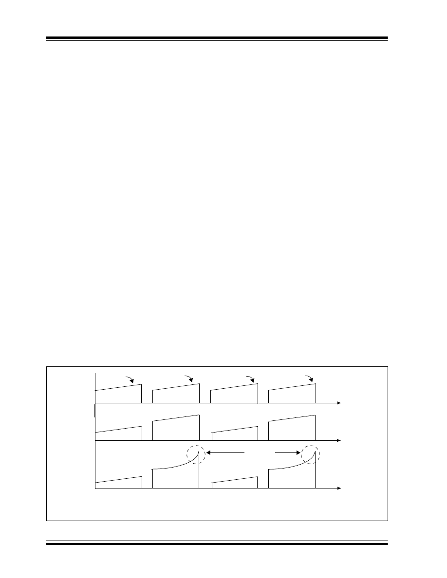
Figure 14 explains how to determine the status of
magnetics imbalance in the core during the steady
state of operation by looking at current waveforms of
the two switches Q
1
and Q
2
. If the current wave shape
of both switches is symmetrical and equal in
magnitude, as shown in Figure 14 (A), the flux
excursion in the core is well balanced and the
transformer is operating in a safe region. However, if
the current wave shape of both switches is not
symmetrical and the peak magnitude current is not
equal, as shown in Figure 14 (B), there is an imbalance
in the flux excursion inside the core; however, it is still
operating at the safe operating region of the BH loop. If
the current wave shape of one of the switches has
upward concavity, as shown in Figure 14 (C), this
means there is a large inequality in the flux excursion
inside the magnetic core, and magnetic BH loop is
close to saturation. A small increase in the magnetic
field intensity H will cause a decrease in magnetizing
inductance, whereas a significant increase in
magnetizing current can destroy the switch and the
transformer.
FLUX DOUBLING AND VOLT-SECOND
CLAMPING
When such a system is first switched ON or during the
load transient, the flux density will start from zero rather
than B
1
or B
2
, and consequently, the available flux
excursion at this instant will be half that normally
available under the steady state condition. This is
called “flux doubling”. The drive and control circuitry
must recognize this condition and protect the
application from wide drive pulses until the normal
working condition of the core is restored. This is known
as “volt-second clamping”.
COPPER UTILIZATION
A push-pull transformer requires a center tapped
primary, and each winding is active only for alternate
power pulses, which means only 50% utilization of
primary copper. The unused copper occupies space in
the bobbin and increases the primary leakage
inductance. A center-tapped primary would normally be
bifilar wound, but this will cause a large AC voltage
between the adjacent turns.
APPLICATION CONSIDERATIONS
The high voltage (2 • V
IN
) stress on the switch, and
50% utilization of the transformer primary makes using
the push-pull topology undesirable when the input
voltage is European, Asian, the universal range (90
V
AC
-230 V
AC
), or when PFC is used as the front end
rectifier. The reason for this is incomplete utilization of
magnetic core, which is due to only one switch
conducting during each switching cycle and full input
voltage is applied across the transformer primary. The
push-pull topology is most favorable for low-voltage
applications such as US regulation 110 V
AC
input direct
off-line SMPS, or low input voltage DC-DC isolated
converter for the power rating of up to 500 watts.
FIGURE 14:
PUSH-PULL CONVERTER SWITCH CURRENT
Q
1ON
Q
2ON
Q
1ON
Q
2ON
IQ
1
IQ
2
IQ
1
IQ
2
Saturation
t
t
t
(A) = Equal volt second is applied across the primary
(B) = Unequal volt second applied across the primary but still in safe region
(C) = Highly unbalance volt second applied across the secondary and core is near to saturation
(C)
(B)
(A)
© 2007 Microchip Technology Inc.
DS01114A -page 19
AN1114
AVOIDING SHOOT-THROUGH
In a push-pull converter, both switches cannot turn ON
at the same time. Turning both switches on at the same
time will generate an equal and opposite flux in the
transformer core, which results in no transformer action
and the windings will behave as if they have a short.
This condition offers a very low impedance between
the input source V
IN
and ground, and there will be a
very large shoot-through current through the switch,
which could destroy it. To avoid shoot-through, an
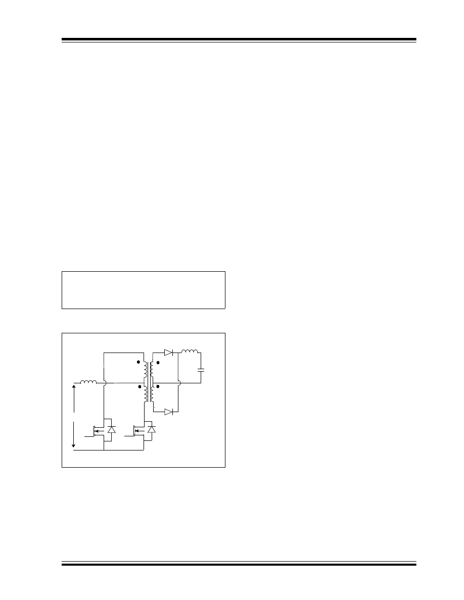
inductor is placed between the transformer primary and
the input supply, as shown in Figure 15. The resulted
converter is known as a current-source push-pull
converter. When both switches are on, the voltage
across the primary becomes zero and the input current
builds up and energy is stored in the inductor. When
only one of the two switches is ON, the input voltage
and stored energy in the inductor supplies energy to
the output stage.
The relation between the output and input in
Continuous Conduction mode is given by Equation 15.
EQUATION 15: CURRENT SOURCE
PUSH-PULL CONVERTER
V
OUT
/V
IN
RELATIONSHIP
FIGURE 15:
CURRENT FED PUSH-PULL
CONVERTER
Half-Bridge Converter
The half-bridge converter is a transformer-isolated
converter based on the basic forward topology. The
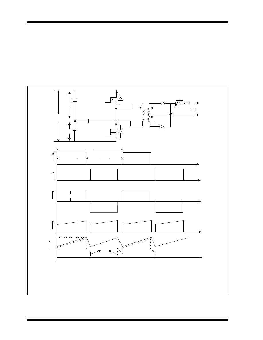
basic schematic and switching waveforms are shown in
Figure 16.
The switches Q
1
and Q
2
form one leg of the bridge, with
the remaining half being formed by the capacitors C
3
and C
4
. Therefore, it is called a half-bridge converter.
The switches Q
1
and Q
2
create pulsating AC voltage at
the transformer primary. The transformer is used to
step down the pulsating primary voltage, and to provide
isolation between the input voltage source V
IN
and the
output voltage. In the steady state of operation,
capacitors C
3
and C
4
are charged to equal voltage,
which results in the junction of C
3
and C
4
being
charged to half the potential of the input voltage.
When the switch Q
1
is ON for the period of T
ON
, the dot
end of the primary connects to positive V
IN
, and the
voltage across the capacitor C
4
(V
C4
) is applied to the
transformer primary. This condition results in half of the
input voltage being V
IN
, which is applied to the primary
when the switch Q
1
is ON, as shown in Figure 16 (C).
The diode D
4
becomes reverse-biased, and the diode
D
3
becomes forward-biased, which carry the full
inductor current through the secondary winding N
S1
.
The difference of the primary voltage reflected on the
secondary N
S1
and output voltage V
OUT
is applied to
the output inductor L in the forward direction.
Therefore, the inductor current I
L
rises linearly from its
present value of I
L1
to I
L2,
as shown in Figure 16 (E).
During this T
ON
period, the reflected secondary current,
plus the primary magnetizing current flows through the
switch Q
1
. As the voltage is applied to the primary in the
forward direction during this T
ON
period, and when the
switch Q
1
is ON, the flux density in the core changes
from its initial value of B
1
to B
2,
as shown in Figure 13.
At the end of the T
ON
period, the switch Q
1
turns OFF,
and remains off for the rest of the switching period T
S
.
The switch Q
2
will be turned ON after half of the
switching period T
S
/2, as shown in Figure 16 (B);
therefore, during the T
OFF
period, both switches are off.
When switch Q
1
is turned off, the body diode of the
switch Q
2
provides the path for the leakage energy
stored in the transformer primary, and the output
rectifier diode D
4
becomes forward-biased. As the
diode D
4
become forward-biased, it carries half of the
inductor current through the transformer secondary
N
S2
and half of the inductor current is carried by the
diode D
3
through the transformer secondary N
S1
, as
shown in Figure 16 (E). Therefore, the equal and
opposite voltage is applied at the transformer
secondary, assuming both secondary windings N
S1
and N
S2
have an equal number of turns. As a result, the
net voltage applied across the secondary during the
T
OFF
period is zero, which keeps the flux density in the
transformer core constant to its value of B
2
.
The output voltage V
OUT
is applied to the inductor L in
the reverse direction when both switches are OFF.
Therefore, the inductor current I
L
decreases linearly
from its initial value of I
L2
to I
L1,
as shown in Figure 16
(E). The body diodes of switches Q
1
and Q
2
provide the
path for the transformer leakage energy.
V
OUT
V
IN
-------------
N
S
N
P
-------
⎝
⎠
⎛
⎞
1
2
1 D
–
(
)
⋅
-------------------------
⎝
⎠
⎛
⎞
⋅
=
V
IN
Q
2
V
OUT
+
-
D
D
5
Q
1
D
N
P2
N
P1
N
S2
N
S1
N
P1
=
N
P2
=
N
P
N
S1
=
N
S2
=
N
S
D
6
I
OUT
AN1114
DS01114A -page 20
© 2007 Microchip Technology Inc.
After the time period T
S
/2 when the switch Q
2
turns ON,
the dot end of the primary connects to the negative of
V
IN
, and the voltage across the capacitor C
3
(V
C3
) is
applied to the transformer primary. Therefore, half of
the input voltage V
IN
is applied to the primary when the
switch Q
2
is ON in the reverse direction, as shown in
Figure 16 (C). The value of the magnetic flux density in
the core is changed from its initial value of B
2
to B
1,
as
shown in Figure 13. Assuming the number of
secondary winding turns of N
S1
is equal to N
S2
, and to
avoid magnetic saturation in the transformer core, the
T
ON
period of both switches should be the same. After
the T
ON
period, Q
2
turns OFF and remains off for the
rest of the period T
S
, as shown in Figure 16 (B). Please
note that when either of the switches turn ON for the
T
ON
period, it affects the entire input voltage V
IN
of the
other switch.
FIGURE 16:
HALF-BRIDGE CONVERTER
V
IN
D
3
I
OUT
+
-
D
4
Q
1
IQ
1
Q
2
L
+
-
IL
IQ
2
C
4
C
3
C
B
V
C3
V
C4
Q
1PWM
Q
2PWM
V
IN
/2
IQ
1
IQ
2
IQ
1
IQ
2
V
P
+
-
V
P
I
L
I
SW
I
D4
t
t
t
t
t
I
L1
I
L2
V
OUT
(A) = Half-Bridge Converter
(B) = Gate pulse waveform of Q
1
(C) = Voltage across transformer primary
(D) = Current through the switch Q
1
and Q
2
(E) = Output inductor and diode D
4
current
(A)
(B)
(C)
(D)
(E)
T
ON
T
OFF
T
S
N
P
N
S1
N
S2
© 2007 Microchip Technology Inc.
DS01114A -page 21
AN1114
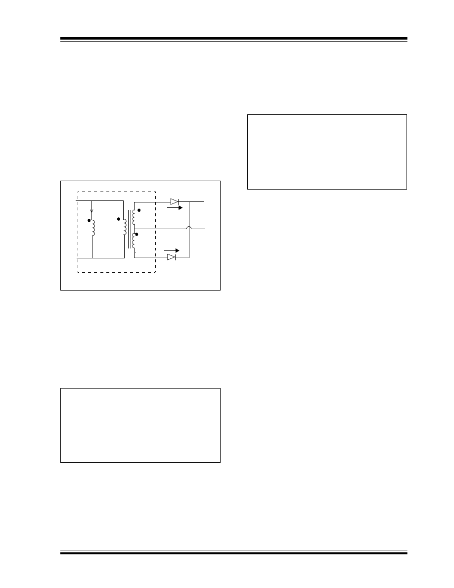
EQUIVALENT TRANSFORMER
The equivalent transformer model is shown in
Figure 17. During the T
OFF
period, when both switches
are OFF, ideally, the secondary currents flowing
through the diode D
3
and the diode D
4
should be equal.
However, in the practical sense, because of the
presence of the non-zero magnetizing current I
M
, I
D3
and I
D4
are not equal.
This magnetizing current I
M
(t), as shown in Figure 17,
may flow through the transformer primary, through one
of the secondaries, or it may divide between all three of
the windings.
FIGURE 17:
TRANSFORMER
EQUIVALENT MODEL
The division of the magnetizing current depends on the
I-V characteristics of the switches, the diode and the
leakage of the transformer windings. Assuming
negligible leakage in the transformer and that both
diodes have similar I-V characteristics, the current
flowing through the diode D
3
and D
4
is given by
EQUATION 16: OUTPUT DIODES AND
MAGNETIZING CURRENT
RELATIONSHIP
DC BLOCKING CAPACITOR
A small DC blocking capacitor is placed in series with
the transformer primary, to block the DC flux in the
transformer core. The value of the DC blocking
capacitor is given by Equation 17.
EQUATION 17: DC BLOCKING CAPACITOR
PREVENTING SHOOT-THROUGH
A half-bridge converter is also prone to magnetic
imbalance of the transformer core when the flux
created by the switches Q
1
and Q
2
during the T
ON
period is not equal. To prevent staircase saturation, the
peak current mode control technique is used to decide
the T
ON
period of the switches Q
1
and Q
2
. The
maximum duty cycle of 45% with a dead-time between
the two switches is used to prevent shoot-through
current from the transformer primary.
APPLICATION CONSIDERATIONS
The complete utilization of the magnetic and
maximum voltage stress on either of the switches is
equal to the input voltage V
IN
. However, only half of
the input voltage is applied across the primary when
either of the switches is ON for the T
ON
period.
Therefore, double the primary switch current is
required to have the same output power as the
push-pull converter. This makes the half-bridge
topology best suited for applications up to 500 watts.
This is especially suited for European and Asian
regions where the AC is 230 V
AC
line voltage. The
power rating of the half-bridge converter can be
increased up to 650-750 watts if front-end PFC is
used. The peak primary current and the maximum
transient OFF state voltage stress of the switch
determine the practical maximum available output
power in the half-bridge converter topology.
I
1
(t)
D
4
N
P
N
S2
N
S1
D
3
i
d3
I
D4
Transformer Equivalent Model
I
1
’
(t)
I
M
(t)
V
P
+
-
N
S
= N
S1
= N
S2
for I
M
(t)<< i
(
t
)
I
1
0
=
I
D3
0.5 i t
( )
0.5 n
⋅
(
)
–
I
M
t
( )
⋅
⋅
=
I
D3
I
D4
0.5 i t
( )
⋅
=
=
I
D4
0.5 i t
( )
0.5 n
⋅
(
)
–
I
M
t
( )
⋅
⋅
=
C
B
I
PRIM
T
ONMAX
⋅
V
Δ
----------------------------------------
=
where:
T
ONMAX
= maximum ON time of either MOSFET
I
PRIM
= maximum primary current
Δ
V = permissible droop in primary voltage because of
the DC blocking capacitor
AN1114
DS01114A -page 22
© 2007 Microchip Technology Inc.
Half-Bridge Resonant Converter
Magnetics and heat sink occupy more than 80% of the
total system volume. High switching frequency and
high efficiency are the two methods used to improve
power density and the profile of a SMPS. However,
these two methods do not come together easily. High
switching frequency (more than 100 kHz) could reduce
the volume of the passive components, but efficiency
often suffers as a result. High EMI noises caused by
parasitic components prevent fast switching. Efficiency
is reduced due to high switching losses, and diode
reverse recovery causes voltage overshoot and ringing
across the device.
IMPROVEMENT TECHNIQUES
To develop SMPS with high efficiency and high
switching frequencies, and to achieve high power
density and low profile, the following techniques need
to be improved.
The size of the magnetic components is limited by
magnetic losses. With the use of better magnetic, the
size of the magnetic could be greatly reduced. With
better semiconductor switching devices like
CoolMOS™, Schottky diode losses in the
semiconductor can be reduced. This lessens the
thermal management requirement as well as reducing
the size and quantity of the heat sink.
Advanced packaging of active and passive
components, such as integration of a capacitor into the
magnetic, integration of output inductor in the isolation
transformer, and the use of the leakage inductance of
the transformer when an inductor is required in series
with transformer winding, contribute to improving
efficiency. In addition, the use of advanced power
topologies, which reduce switching losses at higher
frequencies.
RESONANT TOPOLOGIES
The resonant technique is used to reduce the switching
losses in the semiconductor devices. There are many
resonant topologies available, such as:
• Series resonant converter
• Parallel resonant converter
• LLC resonant converter
The first two topologies cannot be optimized for the
wide input voltage range and wide output load
variation. The LLC resonant converter is capable of
reducing switching losses at wide input voltage range,
and minimizes the circulating energy at high input
voltage. Turn off losses can be minimized by reducing
the turn-off current through the switch and zero voltage
switching (ZVS), thereby eliminating turn-on losses.
Therefore, the LLC resonant converter provides
negligible switching losses at high switching frequency
even at high input voltage variation range.
Series Resonant Converter (SRC)
In a series resonant converter (SRC), resonant tank
elements (the inductor L
R
and the capacitor C
R
), are
connected in series with the transformer primary, as
shown in Figure 18.
FIGURE 18:
SERIES RESONANT
CONVERTER
The resonant tank is used to shape the primary current
as sinusoidal, and to reduce the current value flowing
through the switch at its transition period, thereby
reducing the switching losses. In a power MOSFET,
zero voltage switching is preferred as compared to zero
current switching. Therefore, the operating switching
frequency, more than the resonant tank frequency, is
preferred for this type of converter to achieve ZVS, as
shown in Figure 19. The operating frequency increases
to a very high value at light load (Q = 0) to keep the
output voltage regulated.
FIGURE 19:
DC CHARACTERISTICS
At low input voltage, the converter is operating close to
resonant frequency. As the input voltage increases, the
converter should operate at a higher switching
frequency away from the resonant frequency, thereby
increasing more and more circulation energy in the
resonant tank, as shown in Figure 20.
V
IN
I
OUT
+
-
C
R
N
S
N
S
L
R
V
OUT
.2
.4
.6
.8
1.0 1.2 1.4 1.6 1.8
Q
=
1
Q
=
2
Q
=
3
Q
=
4
V
IN
= 300V
V
IN
= 400V
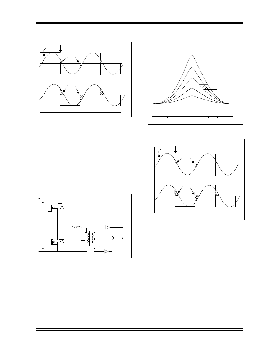
© 2007 Microchip Technology Inc.
DS01114A -page 23
AN1114
FIGURE 20:
CURRENT AND VOLTAGE
WAVEFORM
From this analysis, it can be shown that a series
resonant converter is not a good choice for a front end
DC-DC converter. The major problems are: light load
regulation, high circulating energy and turn-off current
at high input voltage.
Parallel Resonant Converter (PRC)
In a parallel resonant converter (PRC), a resonant tank
element, the capacitor C
R
, is connected in parallel with
the transformer primary, as shown in Figure 21. Similar
to the SRC, the operation switching frequency is also
designed to be more than the resonant tank frequency.
FIGURE 21:
PARALLEL RESONANT
CONVERTER
Compared to SRC, the operating region is much
smaller at a light load (Q =
∞), as shown in Figure 22.
FIGURE 22:
DC CHARACTERISTICS
FIGURE 23:
CURRENT AND VOLTAGE
WAVE FORM
In a parallel resonant converter, since the load is in
parallel with the resonant capacitor, even at no load,
the resonant tank offers very small impedance to the
input, which induces a very high circulation energy.
Given the above analysis, we can determine that a
parallel resonant converter is not a good choice for a
front end DC-DC converter. The major problems are:
high circulating energy and high turn-off current at high
input voltage conditions.
I
R
Circulating
Energy
Circulating
Energy
V
IN
= 300V, full Load
V
IN
= 400V, full Load
V
IN
+
-
N
S
N
S
L
R
V
OUT
I
OUT
C
R
.2
.4
.6
.8
1.0 1.2 1.4 1.6 1.8
V
IN
= 300V
V
IN
= 400V
I
R
Circulating
Energy
Circulating
Energy
V
IN
= 300V, full Load
V
IN
= 400V, full Load
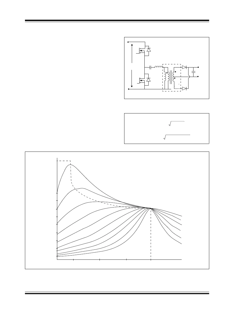
AN1114
DS01114A -page 24
© 2007 Microchip Technology Inc.
LLC Resonant Converter
In an LLC resonant converter, resonant tank elements
(the inductor L
R
and the capacitor C
R
), are connected
in series with the transformer primary, and the resonant
inductor L
M
is connected in parallel with the
transformer primary, as shown in Figure 24.
The LLC resonant converter uses transformer
magnetizing inductance for generating one more
resonant frequency, which is much lower than the main
resonant frequency comprising resonant tank L
R
and
C
R
. The LLC resonant converter is designed to operate
at a switching frequency higher than the resonant
frequency of the resonant tank L
R
and C
R
.
The benefit of the LLC resonant converter is narrow
switching frequency range with light load and ZVS
capability even at no load. In addition, its special DC
gain characteristic, as shown in Figure 25, makes the
LLC resonant converter an excellent choice for the
front end DC-DC application. The two resonant
frequencies are given by Equation 18. The first
resonant frequency is determined by L
R
and C
R
and
the other resonant frequency is determined by L
R
, C
R
and L
M
.
FIGURE 24:
HALF-BRIDGE LLC
RESONANT CONVERTER
EQUATION 18: LLC RESONANT
FREQUENCIES
FIGURE 25:
DC CHARACTERISTIC OF LLC RESONANT CONVERTER
V
IN
+
-
-
C
R
N
S
N
S
L
R
Transformer
Vout
I
OUT
L
M
Q
1
Q
2
D
1
D
2
F
R1
1
2
π
L
R
C
R
⋅
(
)
⋅
⋅
(
)
-----------------------------------------------
=
F
R2
1
2
π
L
M
L
R
+
(
) C
R
⋅
(
)
⋅ ⋅
(
)
-----------------------------------------------------------------
=
.2
.6
.8
1
.2
.4
.6
.8
1.0
1.2
1.4
1.6
1.8
ZCS REGION
ZVS REGION
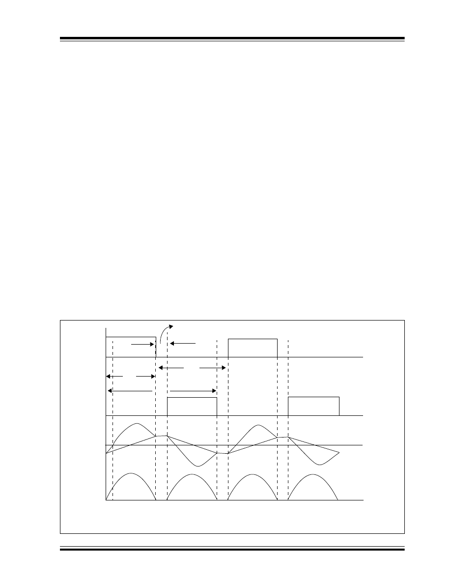
© 2007 Microchip Technology Inc.
DS01114A -page 25
AN1114
LLC Resonant Converter Operation
LLC resonant converter operation can be divided into
two time intervals. In the first interval, the inductor L
R
,
resonant with the capacitor C
R
and inductor L
M
, is
clamped with the output voltage. Resonance of L
R
and
C
R
is stopped when the L
R
resonant current is equal to
the L
M
current, after which L
M
will contribute to the
resonance and the second interval begins. During this
interval, the resonant components will change to C
R
and L
M
in series with L
R
(see the flat region in
Figure 26 (B)). Therefore, the LLC resonant converter
is a multi-resonant converter since the resonant
frequency at particular time intervals is different.
The detailed operation of the LLC resonant converter,
as shown in Figure 26, can be broken down into three
modes. At the initial condition, t = t0, the description of
the LLC resonant converter operation begins at the
conclusion of one power transfer cycle. This occurs
after the resonant tank delivering power to the load with
switch Q
2
is conducting. The resonant current (when
Q
2
is conducting) flowing through the inductor is
negative, as indicated in Figure 26 (B).
• Mode 1: t0 < t < t1 (Q
2
turned OFF at t = t0)
In this mode, the energy stored in the resonant
inductor discharges the output capacitor of the
switch Q
1
to zero potential. The body diode of the
switch provides the path for the resonant inductor
current L
R
, which creates a ZVS condition for
Switch Q
1.
The gate signal of Q
1
should be applied
after the body diode of Q
1
starts conducting.
• Mode 2: t1 < t < t2
This mode begins when inductor current becomes
positive, as shown in Figure 26 (B). Since the
switch Q
1
is turned ON during Mode 1, current will
flow through switch Q
1
. The output rectifier diode
D
1
becomes forward-biased, and the transformer
voltage clamps at output voltage V
OUT
. The
reflected secondary voltage on the primary clamps
L
M
to constant voltage, so it cannot participate in
the resonance during this period. This mode
comes to an end when L
R
current is equal to L
M
current, and the output current reaches zero, as
shown in Figure 26 (C).
• Mode 3: t2 < t < t3
In this mode, when the inductor current L
R
and L
M
are equal and the output current reaches zero,
both output rectifiers become reverse-biased.
During this period, L
M
is freed to contribute to
resonance, and form a resonant tank, C
R
and L
R
in series with L
M
. This mode ends when the switch
Q
1
turns OFF.
As seen in Figure 26 (B), the switch Q
1
turns OFF at a
very low value of current compared with peak current.
ZVS depends on the magnetizing current and not the
load current. This magnetizing current is also the
turn-off current of the switch, which can be controlled to
achieve almost zero turn-off losses. For the next half
cycle, the operation is the same as previously
described.
FIGURE 26:
LLC RESONANT CONVERTER
td = Dead time
T
ON
T
OFF
T
S
t1
t0
t2 t3
(A) = Gate pulse for LLC resonant converter
(B) = Resonant magnetizing current
(C) = Output current
(A)
(B)
(C)
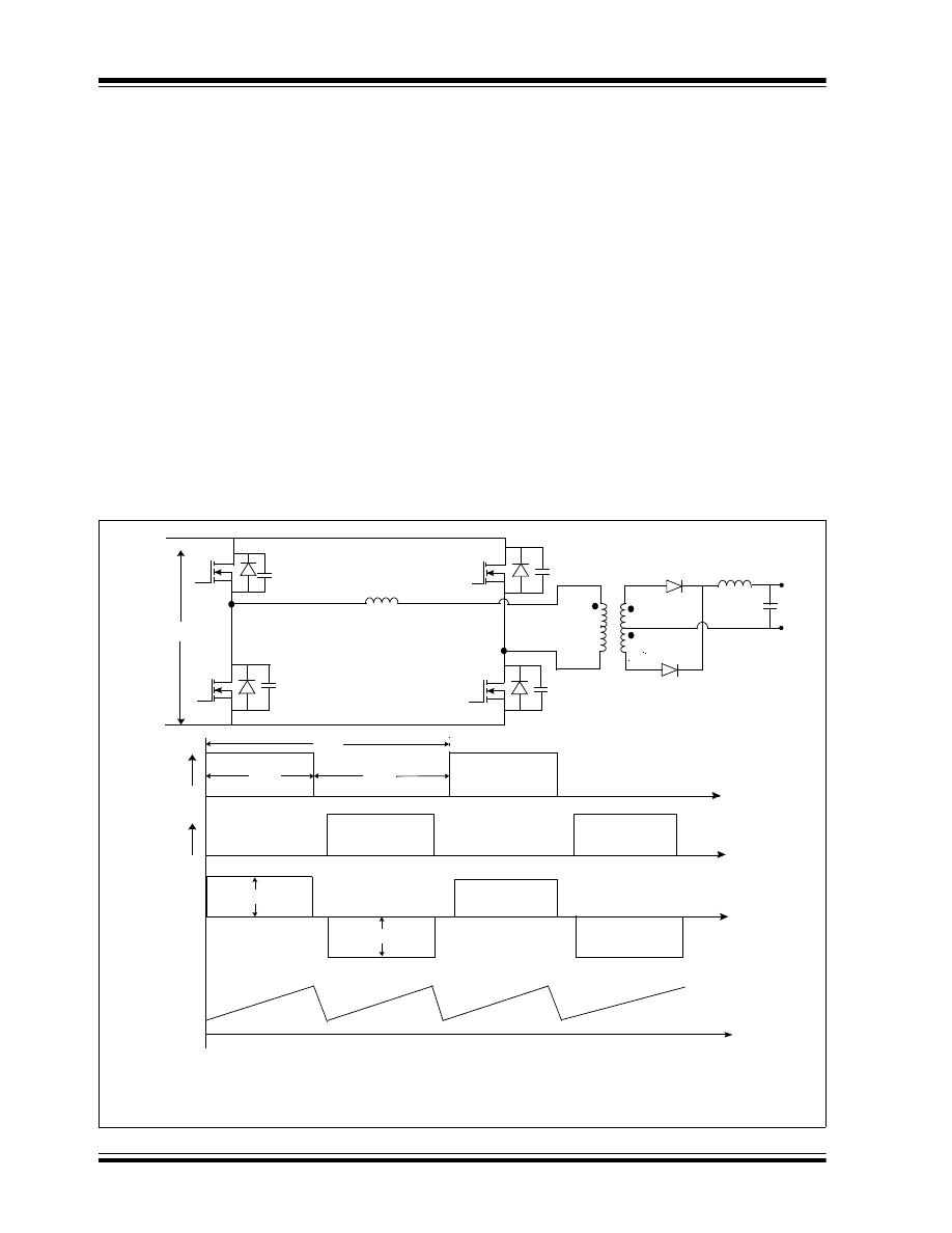
AN1114
DS01114A -page 26
© 2007 Microchip Technology Inc.
Full-Bridge Converter
A full-bridge converter is a transformer-isolated buck
converter. The basic schematics and switching
waveforms are shown in Figure 27. Since the shape of
the converter looks like an H, a full-bridge converter is
also known as an H-bridge converter.
BASIC OPERATION
The transformer primary is connected between the two
legs formed by the switches Q
1
Q
4
and Q
3
Q
2
. The
switches Q
1
Q
2
and Q
3
Q
4
create a pulsating AC
voltage at the transformer primary. The transformer is
used to step down the pulsating primary voltage, as
well as to provide isolation between the input voltage
source and the output voltage V
OUT
. As in half-bridge
topology, the voltage stress on the switch is V
IN
.
However, voltage applied on the primary when either of
the switches is ON is half of the input voltage, thereby
doubling the switch current. In a push-pull topology,
voltage applied on the transformer primary when either
of the switches is ON, is full input voltage; however, the
voltage stress of the switch is twice the input voltage.
This condition renders both topologies unfeasible for
high power (>500 watt) applications.
A full-bridge converter configuration retains the voltage
properties of the half-bridge topology, and the current
properties of push-pull topology. The diagonal switch
pairs, Q
1
Q
2
and Q
3
Q
4,
are switched alternately at the
selected switching period. In the steady state of
operation when the diagonal switch pair, Q
1
Q
2,
is ON
for a period of T
ON
, the dot end of the winding becomes
positive with respect to the non-dot end. The diode D4
become reverse-biased and diode D3 becomes
forward-biased. The diode D3 carries the full load
current through the secondary winding N
S1
. As the
input voltage is applied across the transformer primary,
the switch carries the reflected load current, plus the
transformer primary magnetizing current. The flux
density in the core changes from its initial value of B
1
to
B
2,
as shown in Figure 13. The difference of the
primary reflected voltage to the secondary and the
output voltage is applied across the inductor L in the
forward direction.
FIGURE 27:
FULL-BRIDGE/H-BRIDGE PHASE SHIFT ZVT CONVERTER
V
IN
D
3
+
-
D
4
Q
3
Q
2
L
+
V
L
Q
1PWM
Q
2PWM
V
IN
Q
1
Q
4
V
IN
Q
3PWM
Q
4PWM
C
OSS1
C
OSS4
C
OSS2
C
OSS3
L
LKG
(A) = Full-Bridge/H-Bridge Phase Shift ZVT converter
(B) = PWM gate pulse waveform for full-bridge switches
(C) = Voltage across the transformer primary
(D) = Output inductor and rectifier diode current
(A)
(B)
(C)
(D)
-
C
O
V
OUT
T
ON
T
OFF
T
S

© 2007 Microchip Technology Inc.
DS01114A -page 27
AN1114
At the end of the ON period, when the switch pair Q
1
Q
2
is turned OFF, and when it remains OFF for the rest of
the switching period T
S
, the switch pair Q
3
Q
4
will be
turned ON after half of the switching period T
S
/2, as
shown in Figure 27(B and C). Therefore, during the
T
OFF
period, all four switches are OFF.
When the switch pair Q
1
Q
2
is turned OFF, the body
diode of the switch pair Q
3
Q
4
provides the path for the
leakage energy stored in the transformer primary.The
output rectifier diode D4 becomes forward-biased, and
it carries half of the inductor current through the
transformer secondary N
S2.
Half of the inductor current
is carried by the diode D3 through the transformer
secondary N
S1,
as shown in Figure 27 (D). Therefore,
the net voltage applied across the secondary during
T
OFF
period is zero as previously discussed in
half-bridge topology operation. This keeps the flux
density in the transformer core constant to its final
value of B
2
(see Figure 15). The output voltage V
OUT
is
applied to the inductor L in the reverse direction when
both switches are OFF.
After the time period T
S
/2, when the diagonal switch Q
3
,
Q
4
is turned ON for a period of T
ON
, the dot end of the
winding becomes negative with respect to the non-dot
end. The diode D3 becomes reverse-biased and the
diode D4 becomes forward-biased. The diode D4 car-
ries the full load current through the secondary winding
N
S2
. As the input voltage is applied across the trans-
former primary, the switch carries the reflected load
current plus the transformer primary magnetizing cur-
rent. As the input, voltage is applied to the transformer
in the reverse direction, the flux density in the core
changes from its initial value of B
2
to B
1,
as shown in
Figure 13. The difference of the primary reflected volt-
age to the secondary and the output voltage is applied
across the inductor L in forward direction.
Assuming the number of secondary winding turns N
S1
is equal to N
S2
, and to avoid magnetic saturation in the
transformer core, the T
ON
period of both switch pairs Q
1
Q
2
and Q
3
Q
4
should be equal. After the T
ON
period of
the switch pair Q
3
Q
4
, it turns OFF and remains OFF for
the rest of the period T
S
, as shown in Figure 27 (B).
Please note that when either of the diagonal switch
pairs turns ON for a period of T
ON
, it applies the entire
input voltage V
IN
to the other switch.
In Continuous Conduction mode of operation, the
relation between the input voltage and the output
voltage is given by Equation 19.
EQUATION 19: FULL-BRIDGE CONVERTER
V
OUT
/
VIN
RELATIONSHIP
APPLICATION CONSIDERATIONS
Since the maximum voltage stress across any switch is
V
IN
, and with the complete utilization of magnetic core
and copper, this combination makes the full-bridge con-
verter an ideal choice for high input voltage, high power
range SMPS (<1000 watts) applications.
Full-Bridge Converter
In the full-bridge converter, four switches have been
used, thereby increasing the amount of switching
device loss. For applications requiring output power of
more than 1000 watts, the loss in the switching device
becomes impractical to handle in a full-bridge
converter.
The conduction loss of a MOSFET can be reduced by
using a good MOSFET, and switching losses can be
reduced by using either a ZVS (zero voltage switching
during turn ON transition), a ZCS (zero current
switching during turn OFF transition), or both
techniques. Shaping the input current sinusoidal to
achieve ZCS, increases the peak and the RMS current
through the MOSFET in the high power application,
thereby increasing the conduction losses. At high input
voltage, the ZVS technique is preferred for the
MOSFET.
Full-Bridge/H-Bridge Phase-Shift ZVT Topology
A full-bridge converter using the phase shift ZVT
technique is known as an H-Bridge Phase-Shift ZVT
topology. In this topology, the parasitic output capacitor
of the MOSFETs and the leakage inductance of the
switching transformer are used as a resonant tank
circuit to achieve zero voltage across the MOSFET at
the turn-on transition. There are two major differences
in the operation of a phase-shift ZVT and simple
full-bridge topology. In a phase-shift ZVT converter, the
gate drive of both of the diagonal switches is phase
shifted. In addition, both halves of the bridge switch
network are driven through the complementary gate
pulse with a fixed 50% duty cycle. The phase difference
between the two half-bridge switching network gate
drives control the power flow from primary to
secondary, which results in the effective duty cycle.
Power is transferred to the secondary only when the
diagonal switches are ON. If either the top or bottom
switches of both legs are ON simultaneously, zero
voltage is applied across the primary. Therefore, no
power is transferred to the secondary during this
period. When the appropriate diagonal switch is turned
OFF, primary current flows through the output capacitor
of the respective MOSFETs causing switch drain volt-
age to move toward to the opposite input voltage rail.
This causes zero voltage across the MOSFET to be
turned ON next, thus creating zero voltage switching
when it turns ON. This is possible when enough circu-
lating current is provided by the inductive storage
energy to charge and discharge the output capacitor of
V
OUT
2 V
IN
N
S
N
P
-------
⎝
⎠
⎛
⎞ D
⋅
⋅
⋅
=
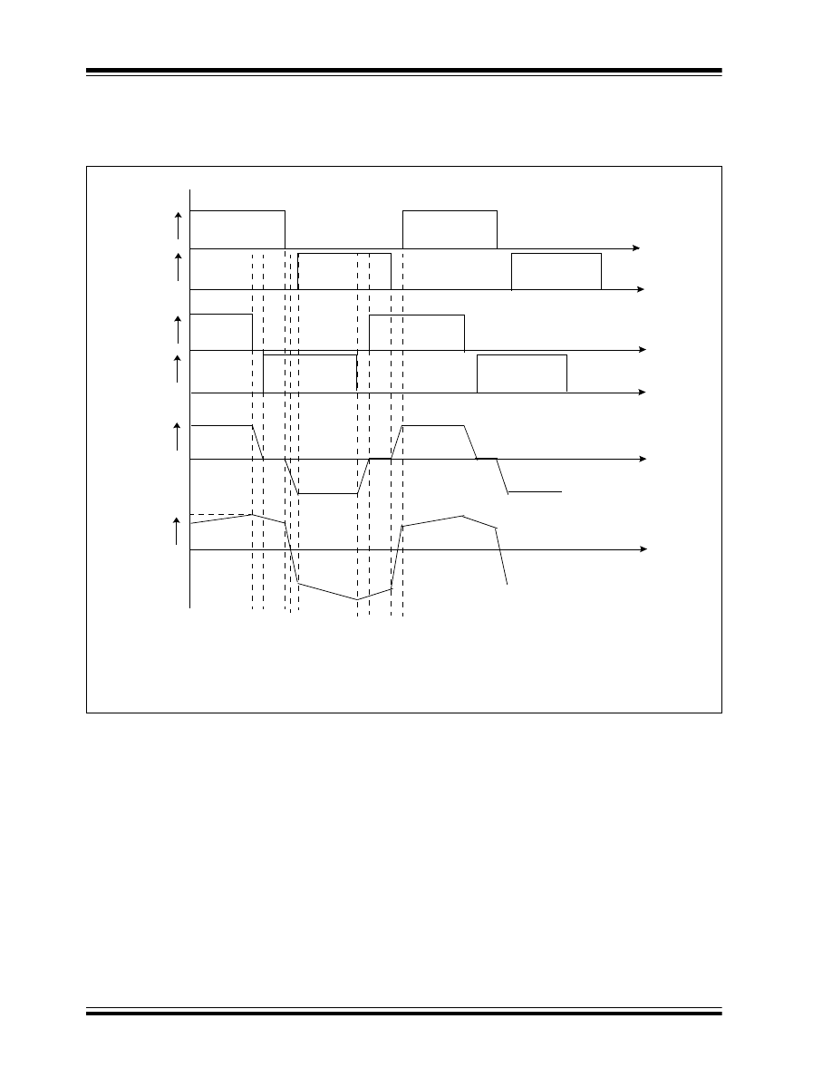
AN1114
DS01114A -page 28
© 2007 Microchip Technology Inc.
the respective MOSFETs. Figure 28 shows the gate
pulse required, and the voltage and current waveform
across the switch and transformer.
FIGURE 28:
REQUIRED GATE PULSES AND VOLTAGE AND CURRENT ACROSS PRIMARY
Q
1PWM
Q
4PWM
Q
2PWM
Q
3PWM
V
PRIMARY
I
P
t0 t1 t2 t3 t4
I
PK
(A) = Gate pulse for all switches for phase-shift ZVT converter
(B) = Voltage across primary
(C) = Current across primary
(A)
(B)
(C)

© 2007 Microchip Technology Inc.
DS01114A -page 29
AN1114
TIME INTERVALS
The operation of the phase-shift ZVT can be divided
into different time intervals. Assuming that the
transformer was delivering the power to the load, the
current flowing through primary is I
PK
, and the diagonal
switch Q
1
, Q
2
was ON, at t = t0, the switch Q
2
is turned
OFF.
• Interval1: t0 < t < t1
The switch Q
2
is turned OFF, beginning the
resonant transition of the right leg. Primary current
is maintained constant by the resonant inductor
L
LK
. This primary current charges the output
capacitor of switch Q2 (C
OSS2
) to the input voltage
V
IN
, which results in the output capacitance of Q
3
(C
OSS3
) being discharged to zero potential. This
creates zero potential across the switch Q
3
prior to
turn-on, resulting in zero voltage switching. During
this transition period, the transformer primary
voltage decreases from V
IN
to zero, and the
primary no longer supplies power to the output.
Inductive energy stored in the output inductor and
zero voltage across the primary cause both output
rectifiers to share the load current equally.
• Interval2: t1 < t < t2
After charging C
OSS2
to V
IN
, the primary current
starts flowing through the body diode of Q
3
. Now
Q
3
can be turned on any time after t1 and have a
zero voltage turn-on transition.
• Interval3: t2 < t < 3
At t = t2, Q
1
was turned OFF and the primary was
maintained by the resonant inductor L
LK
. In
addition, at t = t2,
I
P
is slightly less than the
primary peak current I
PK
because of finite losses.
The primary resonant current charges the output
capacitor of switch Q
1
(C
OSS1
) to input voltage V
IN
,
which discharges the output capacitor of Q
4
(C
OSS4
) to zero potential, thus enabling zero
voltage turn-on switching for Q
4
. During this
transition, the primary current decays to zero. ZVS
of the left leg switches depends on the energy
stored in the resonant inductor, conduction losses
in the primary switches, and the losses in the
transformer winding. Since this left leg transition
depends on leakage energy stored in the
transformer, it may require an external series
inductor if the stored leak energy is not enough for
ZVS. Now, when Q
4
is turned ON, voltage V
IN
is
applied across the primary in the reverse direction.
• Interval: t3 < t < t4
The two diagonal switches Q
3
, Q
4
are ON,
applying full input voltage across the primary.
During this period, the magnetizing current, plus
the reflected secondary current into the primary
flows through the switch. The exact diagonal
switch-on time T
ON
depends on the input voltage,
the transformer turns ratio, and the output voltage.
After the T
ON
period of the diagonal switch, Q
3
is
turned OFF.
One switching cycle is completed when the switch Q
3
is turned OFF. The primary current charges C
OSS3
to a
potential of input voltage V
IN
and discharges C
OSS2
to
zero potential, thereby enabling ZVS for the switch Q
2
.
The identical analysis is required for the next half cycle.
ACHIEVING ZVT
In the H-Bridge Phase Shift ZVT Converter shown in
Figure 27 (A), the maximum transition time occurs for
the left leg at minimum load current and maximum input
voltage, and minimum transition time occurs for the
right leg at maximum load current and minimum input
voltage. Therefore, to achieve ZVT for all switches,
enough inductive energy must be stored to charge and
discharge the output capacitance of the MOSFET in
the specified allocated time. Energy stored in the
inductor must be greater than the capacitive energy
required for the transition as given by Equation 20. The
MOSFET output capacitance varies as applied
drain-to-source voltage varies. Thus, the output
capacitance of the MOSFET should be multiplied by a
factor of 4/3 to calculate the equivalent output
capacitance.
EQUATION 20: RESONANT ELEMENTS L
R
AND C
R
RELATIONSHIP
0.5 L
R
I
PRIMIN
2
C
R
>
V
INMAX
2
⋅
⋅
⋅
L
R
I
PRIMIN
2
C
R
>
V
INMAX
2
⋅
⋅
where:
LR = equivalent leakage inductor
CR = equivalent capacitor required to charge and
discharge
= output capacitor of two switches in parallel
with parasitic
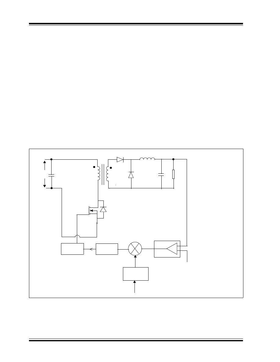
AN1114
DS01114A -page 30
© 2007 Microchip Technology Inc.
METHOD OF CONTROL
All switching converter output voltage is a function of the
input voltage, duty cycle and load current, as well as
converter circuit component values. The output voltage
should be constant regardless of variation in input
voltage, load current and converter circuit parameter
values. The input voltage may vary from 90 V
AC
to 264
V
AC
, and input frequency from 47 Hz to 63 Hz for an
off-line power supply, and -25% to +50% from the
nominal value for the DC input supply. The load current
may vary from no load to full load. In addition, the load
may vary from no load to 50% load in step, and vice
versa. The converter circuit components will have some
tolerance. Despite variation, it is desired that the output
voltage be within a certain limit. This is not practical to
achieve without negative feedback, and setting the duty
cycle to a single value. There are two basic methods to
control the duty cycle to keep the output voltage within
the specified limit: voltage mode control and current
mode control.
Voltage Mode Control
In voltage mode control, the output voltage is
measured and then compared with the reference value
(desired output voltage). The error is then processed
by the compensation block to generate the next duty
cycle value, as shown in Figure 29. This mode has only
one control loop, so it is easy to design and analyze.
However, in this control method, any change in the line
or the load must be first sensed as an output voltage
change and then corrected by the feedback loop.
Therefore, the response is slow and the transient
response (step load change) is not favorable. Adding
input voltage feed-forward to this control scheme will
reduce the effect of input voltage variation in the output.
FIGURE 29:
VOLTAGE MODE CONTROL
V
OUT
V
IN
Load
Drive Circuit
Comparator
Block
V
REF
x
x
Compensator
Block
Output
Voltage
Voltage
Feed Forward
Block
V
IN
-
+
Reference
PWM
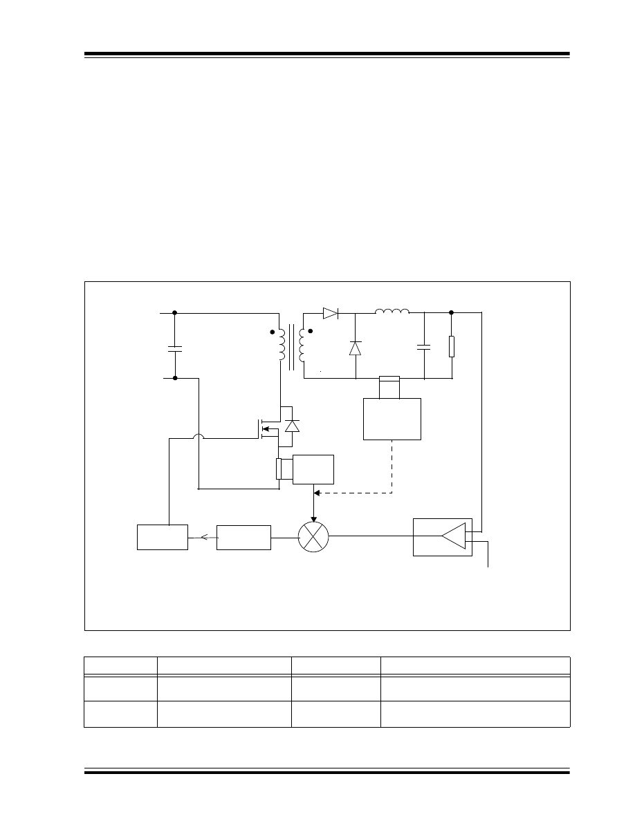
© 2007 Microchip Technology Inc.
DS01114A -page 31
AN1114
Current Mode Control
The current mode control technique requires two
feedback loops, as shown in Figure 30. In this mode,
two parameters are measured for control purposes. The
output voltage is measured at the output capacitor or at
the load end (known as remote sensing). The output
inductor/primary switch current is also measured.
In current mode control, the output voltage is first
compared with the reference voltage (desired output
voltage). This error is then processed by the
compensation block to generate the reference signal
for the current loop. This current reference is compared
to the measured current. Any error generated by the
comparison of the reference generated by the voltage
compensation block and the actual current drawn from
the input is processed by the current compensation
block. This generates the required duty cycle to
maintain the output voltage within the specified limit. As
current mode control senses the circuit current, any
change in output load current or the input voltage can
be corrected before it affects the output voltage.
Sensing the input current, which depends on input
voltage, provides the inherent feed-forward feature.
Current mode control provides inherent input current
symmetry for the push-pull and bridge converters,
inherent current limiting features and load sharing
features for multiple converters connected in parallel. It
also improves step load response and transient
response because of the inner current loop.
FIGURE 30:
CURRENT MODE CONTROL
TABLE 1:
CONTROL METHODS AND CHARACTERISTICS
Mode
Converter
Speed
Description
Voltage
Buck, Forward
Slow
Output short protection, no pulse by pulse
protection
Current
Boost, Flyback, Push-Pull,
Half- and Full-bridge
Fast
Output short circuit and OC protection, pulse
current protection
V
OUT
V
IN
R
S
Load
Drive Circuit
Compensator
Block
I
ERR
Compensator
Block
Output
Voltage
Current
amplifier
sense
Current sense
amplifier with
isolation
I
REF
PWM
+
-
R
S
reference
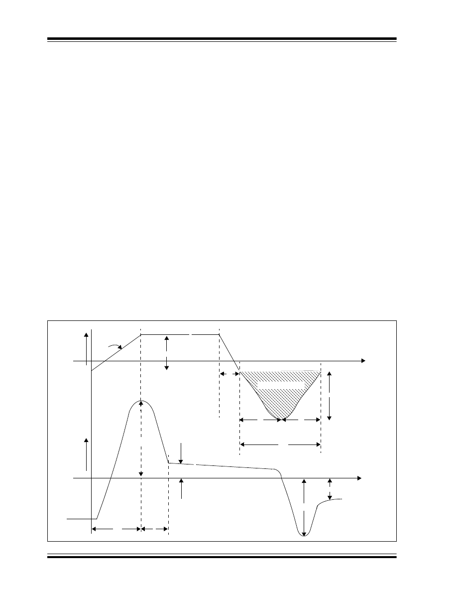
AN1114
DS01114A -page 32
© 2007 Microchip Technology Inc.
Power Diode
A power diode requires a finite time to change from the
blocking state to the conduction state and vice versa.
The time required to change its state, and how the
diode current and voltage change during the transition
period affects the operation of circuitry. The shape of
the waveform (voltage and current) and transition time
depends on diode intrinsic properties.
CHARACTERISTICS
Figure 31 shows how the voltage and current varies in
the power diode during the transition period. During the
period t1, space charge is stored in the depletion region
due to the growth of forward current and removal of
reverse voltage. During period t2, because of diode
forward current, excess carriers distributed in the drift
region settle toward a steady state value. If a large
ΔI/Δt
is applied to the diode, voltage overshoot is observed
due to the presence of ohmic resistance in the drift
region, the inductance of the silicon wafer and the
bonding wires attached to it.
At the turn-off transition, as shown in Figure 31, and
during the period t3, the excess charge stored in the
drift region is removed before the junction becomes
reverse-biased during period t4. This recombination
process of the depletion layer acquires a substantial
amount of charge from the reverse-biased voltage. As
long as there is excess charge in the drift region diode,
it will be forward-biased.
After the t4 junction becomes reverse-biased, and after
the time period t4, the diode current no longer goes
negative and quickly falls and becomes zero after t5.
Reverse recovery current reaches its maximum value
at the end of t4. In almost all of the power circuit
configurations, this reverse recovery current of the
diode will flow through the next MOSFET to turn ON.
So, while fixing the MOSFET current rating, the reverse
recovery current of the diode must be added.
A Schottky diode is a majority carrier device and has no
stored minority carrier; therefore, a Schottky diode
turns ON and OFF faster than a P
N
junction power
diode. A Schottky diode also improves the switching
characteristics and the forward voltage drop of the
diode by placing a thin film of metal in direct contact
with a semiconductor.
The forward voltage drop of a Schottky diode is
0.3-0.4V, and has a larger reverse current than the
comparable silicon power diode. Because of its
physics, the breakdown voltage of the Schottky diode
at present cannot be more than 150-200V. At turn-off
there will be no reverse recovery current because there
is no stored charge. Ohmic resistance of the drift region
is much less than that of the P
N
junction diode,
resulting in considerably less voltage overshoot during
device turn ON.
The diode total loss in the circuit is given by
Equation 21, which consists of forward voltage drop
loss, reverse recovery loss, and reverse leakage
current loss.
FIGURE 31:
POWER DIODE SWITCHING CHARACTERISTICS
Q
RR
= I
RR
• T
RR
/2
0
V
F
0
V
ON
t
V
FP
~ ~
t
1
t
2
t
4
t
5
T
RR
I
RR
V
RR
V
R
I
F
I
F
t
~ ~
ΔI
F
/
ΔT
t
3
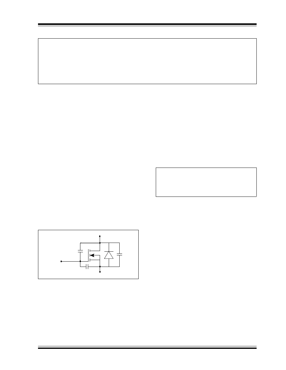
© 2007 Microchip Technology Inc.
DS01114A -page 33
AN1114
EQUATION 21: DIODE LOSS
MOSFET
Appreciable current carrying capability, high reverse
blocking voltage, very low ON resistance and fast
switching capabilities make a MOSFET an ideal choice
as a switching element in SMPS topologies.
A MOSFET is a majority carrier and a voltage driven
device, whereas a Bipolar Junction Transistor (BJT) is
a minority carrier and a current driven device. The ON
state resistance of a MOSFET has no theoretical limit,
so the ON state loss can be far lower than a BJT. The
ON and OFF switching time of a MOSFET depends on
the presence or absence of a key charge quantity in the
device, and is equal to the time required to insert or
remove this controlling charge quantity.
The total amount of controlling charge in the majority
carrier device is much less than the charge required in
the equivalent minority carrier device. This causes the
majority charge carrier device to turn ON and OFF
faster than a minority carrier device. A MOSFET has
positive temperature coefficient for the ON state
resistance, which makes it easy to parallel many small
devices to deliver higher current. Figure 32 shows an
equivalent circuit diagram of a MOSFET with a
parasitic capacitor and body diode.
FIGURE 32:
MOSFET
The turn-on switching waveforms of the drain-to-source
voltage and drain current with gate-to-source voltage
are shown in Figure 33. The rate of change of drain
current depends on the rate at which the gate-to-source
capacitor is charged by the gate drive circuit.
The time required to charge the gate capacitor to V
GTH
(gate threshold voltage) is known as turn-on delay (td).
This assumes the gate drive voltage rises from zero to
V
G
at t = t0, and it is driving the MOSFET gate through
gate resistance R
G
.
After C
GS
is charged to V
GTH
, the drain current begins
rising from zero to the rated value. During this period,
the gate current charges both capacitors, C
GS
and
C
GD
. The drain-to-source voltage remains at V
DS
so
long as the drain current (I
D
) reaches the rated value
(I
D
). The time required for drain current to reach its
rated value ‘I
D
’, as shown in Figure 33, is known as the
current rise time T
RI
. When drain current reaches I
D
,
V
GS
is clamped to V
GS
I
D
, as shown in Figure 33, and
the entire gate current starts flowing through C
GD
to
charge it. This causes the drain-to-source voltage V
DS
to drop. The rate of change of V
DS
is given by
EQUATION 22: RATE OF CHANGE OF V
DS
V
DS
decreases V
D
to V
DSON
in two intervals. The first
interval is known as the active region and the second
interval is known as the transient ohmic region. Once
the MOSFET enters the ohmic region, the
gate-to-source voltage starts to rise toward V
G
, while
simultaneously, the gate current decays to zero. In a
practical system, the freewheeling diode has some
reverse recovery current I
RR
. At this moment, during
the drain current rising period, the drain current rises to
the value I
D
+ I
RR
, and then V
DS
starts to decay to
V
DSON
. After the decay of the reverse recovery current
to zero, I
D
clamps to L
D
.
The sequence is reversed when the MOSFET is turned
OFF. The gate-to-source voltage first decays to V
GS
I
D
,
and then the drain-to-source voltage starts rising
toward V
DS
, as shown in Figure 34. When the
drain-to-source voltage reaches its rated value, V
DS
,
the drain current begins to decay toward zero, and the
gate-to-source voltage and gate current decays to
zero, as shown in Figure 34. The time required for the
gate source voltage to reach V
GS
I
D
is known as turn-off
delay.
P
LOSS
V
F
I
FAVG
0.5 t5 V
R
I
REC
F I
REVAVG
V
R
⋅
+
⋅
⋅
⋅
⋅
+
⋅
=
where:
P
LOSS
= Total diode loss
V
F
= Forward voltage drop
I
FAVG
= Average forward current
V
R
= Reverse blocking applied across the diode
I
REC
= Peak reverse recovery current
Gate (G)
Drain (D)
Source (S)
C
GD
C
DS
C
GS
I
GATE
V
G
V
GSID
–
(
)
R
G
---------------------------------
=
V
DS
Δ
t
Δ
-------------
I
G
C
GD
-----------
=

AN1114
DS01114A -page 34
© 2007 Microchip Technology Inc.
MOSFET LOSSES
There are three types of losses in a MOSFET:
conduction loss, switching loss and gate charge loss.
At low frequencies, conduction loss is dominant, but as
we begin switching at frequencies between 100-150
kHz, switching and gate charge losses start
contributing a significant amount of power dissipation.
The total losses in a MOSFET in power electronic
circuitry is given by Equation 23.
Conduction Loss
Conduction loss depends on the ON state resistance of
MOSFET (R
DSON
), which can be reduced by selecting
a low R
DSON
MOSFET.
Switching Loss
The switching losses of the MOSFET are given by the
area under the waveforms of V
DS
and I
D
, shown
shaded in Figure 33 and Figure 34, and the charge
stored in the parasitic output capacitor C
DS
during the
turn OFF period of the MOSFET. The switching losses
of the MOSFET can be reduced by selecting a
MOSFET with lower C
DS
capacitance and shifting the
current I
D
and the voltage V
DS
waveform to reduce the
overlap period during transition.
Gate Charge Loss
Gate charge loss is caused by charging the gate
capacitance and then dumping the charge to ground in
every switching cycle.
APPLICATION CONSIDERATIONS
A lower R
DSON
device comes with high gate
capacitance and the driver has to charge bigger gate
capacitance, which means a longer turn-on and
turn-off time, resulting in more switching losses. The
general rule of faster switching time to reduce the
switching loss will cause high frequency noise
because of high
ΔV/Δt and high ΔI/Δt, which may
cause an increase of the EMI filter size.
The safe operating area (SOA) of a MOSFET is
decided by maximum drain current I
DMAX
, Internal
junction temperature T
J
, and the breakdown voltage
BV
DS
rating. There is no second breakdown voltage in
a MOSFET as in the case of IGBT, and the SOA of the
MOSFET remains the same in the reverse direction. In
addition, a MOSFET can conduct in either direction
while keeping the same R
DSON
.
While selecting a MOSFET driver, care must be taken
to ensure that the driver can source and sink the
maximum peak current required by a MOSFET gate to
turn ON and OFF in a given specified time. A MOSFET
gate needs large current as the device turns ON, and
for the rest of the period, a high gate-to-source voltage
at low current level.
EQUATION 23: MOSFET LOSS
P
SW
I
DRMS
2
R
DSON
0.5 V
DS
I
D
T
RISE
T
FALL
+
(
) f
SW
0.5 V
DS
2
C
DS
f
SW
Q
GTOTAL
V
G
f
SW
⋅
⋅
+
⋅
⋅
⋅
+
⋅
⋅
⋅
⋅
+
⋅
=
where:
I
DRMS
= Drain RMS current
T
RISE
= Rise time
T
FALL
= Fall time
f
SW
= Switching frequency
Q
GTOTAL
= Total gate charge
C
DS
= MOSFET output capacitor
V
DS
= Drain-to-source voltage
I
D
= Drain current
V
G
= Gate voltage
R
DSON
= ON state resistance of the MOSFET
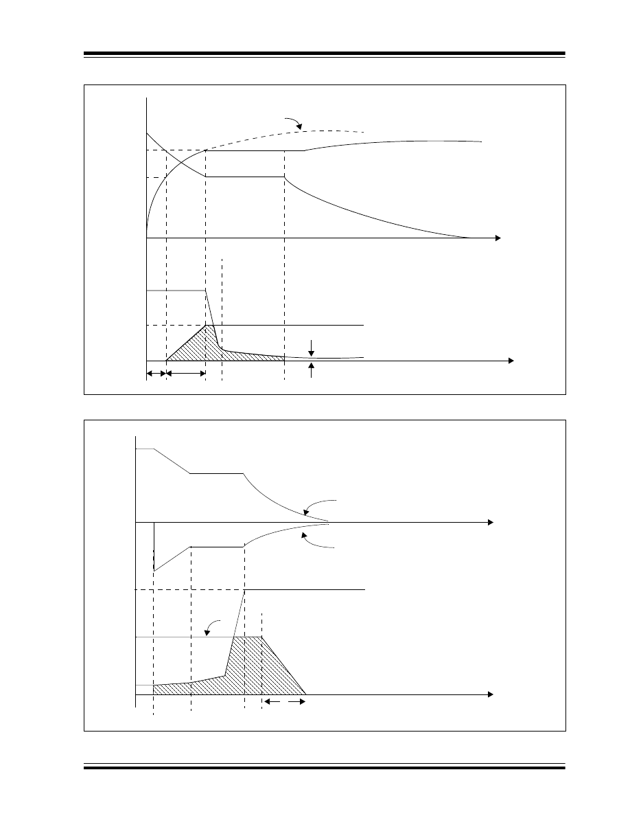
© 2007 Microchip Technology Inc.
DS01114A -page 35
AN1114
FIGURE 33:
MOSFET TURN ON CHARACTERISTICS
FIGURE 34:
MOSFET TURN OFF CHARACTERISTICS
τ
1
= R
G
(C
GD
+ C
GS
)
V
G
V
GS
(I
D
)
0
0
td(on)
V
GS
(th)
I
D
V
D
t
t
V
GS
(t)
I
G
(t)
T
RI
V
DS
(on)
I
G
(t)
V
GS
(t)
T
FI
I
D
(t)
V
DS
(t)
I
D
t
t
V
DS
V
G
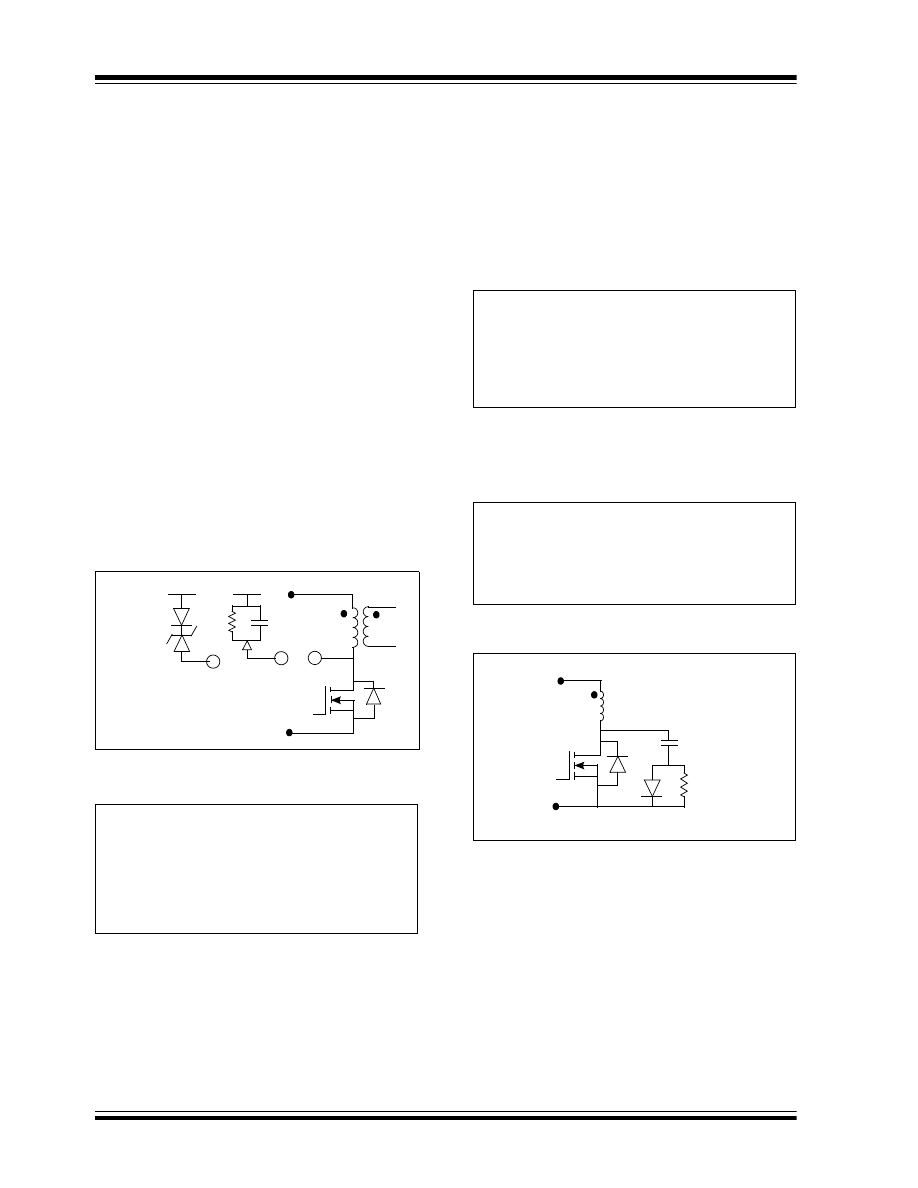
AN1114
DS01114A -page 36
© 2007 Microchip Technology Inc.
Snubbers
There are two basic ways to solve the problem of a
semiconductor device that is stressed beyond its
rating. Either the device can be replaced with a higher
rated device to meet the stress level, or a snubber
circuit can be added to reduce the stress to a safe level.
Both options are trade-offs between cost, availability of
the higher rated device, complexity, component count
and the cost of using a snubber circuit.
A snubber circuit is typically used to limit the rate of rise
of voltage (
ΔV/Δt), the voltage applied across the
device during turn-off, the rate of rise of current (
ΔI/Δt)
and the current through the device during turn-on.
Figure 35 shows some of the popular snubber circuitry
used across the transformer primary in a single switch
power converter application to limit the
ΔV/Δt and
blocking voltage applied across the MOSFET during
turn-off.
The simple design of the RCD snubber, as shown in
Figure 35 (A), is to first choose the capacitor C
S
large
enough so that it contains negligible switching ringing,
and then choose R
S
so that the power dissipated in R
S
at V
S
(voltage across the capacitor C
S
) is equal to the
switching loss caused by the leakage inductance as
given in Equation 24.
FIGURE 35:
TURN OFF SNUBBERS
EQUATION 24: SNUBBER RESISTOR
SELECTION
Figure 36 shows the common turn-off snubber circuitry
used to limit the
ΔV/Δt and reduce the switching losses
in the MOSFET. When the MOSFET turns OFF, some
of the peak current starts flowing through C
S
, which
causes it to slow the drain voltage rise time, and reduce
the area under the V
DS
and I
D
during turn-off time. C
S
has to completely discharge during the minimum T
ON
time of the MOSFET, which limits the maximum value
of C
S
that can be used, is given by Equation 25.
EQUATION 25: SNUBBER CAPACITOR
When the MOSFET turns OFF, C
S
charges to voltage
V
S
, so energy is dissipated during each switching cycle
in the snubber resistor is given by Equation 26.
EQUATION 26: SNUBBER POWER LOSS
FIGURE 36:
MOSFET TURNS OFF
SNUBBER
V
IN
V
IN
V
IN
1
1
1
Q
(A)
(B)
where:
I = The current flowing through the transformer primary
just before the MOSFET turns off
L
LK
= L
LEAKAGE
inductance of the transformer
V
S
2
R
S
--------
0.5 L
LK
I
2
f
SW
⋅
⋅
⋅
=
where:
R
S
= Snubber resistor
C
S
= Snubber capacitor
T
ONMIN
= Minimum ON time of switch
C
S
T
ONMIN
4 R
S
⋅
--------------------
=
P
RS
0.5 V
S
2
C
S
f
SW
⋅
⋅
⋅
=
where:
V
S
= Voltage across the snubber capacitor C
S
f
SW
= Switching frequency
C
S
R
S
D
S
Q

© 2007 Microchip Technology Inc.
DS01114A -page 37
AN1114
MAGNETICS DESIGN
This section covers the basics of magnetic design used
in SMPS applications. After selecting the topology that
is best suited to the power supply specification, the
next choice is to fix the switching frequency and
transformer core size. To do this, it is necessary to
know the numerical relation between maximum
available power and transformer parameters such as
magnetic core area, magnetic length, window area,
bobbin area, peak flux density and coil current density.
There are two types of magnetic losses: hysteresis and
eddy current. Ferrite has high electrical resistivity, so
typically there are only negligible hysteresis and eddy
current losses. This makes ferrite a good material to
use for a switching frequency of 10 kHz to 1 MHz.
Table 2 lists some of the pros and cons of the magnetic
material used in high frequency transformer and
inductor design.
TABLE 2:
MAGNETICS MATERIAL AND THEIR CHARACTERISTICS
Material
Pros
Cons
Ferrite
High permeability, thus can be used to generate
high inductance, permeability is relatively
constant with flux density, and variety of ferrite is
available optimized for minimum power
dissipation for various frequencies. Generally
used for power transformers.
Ferrite saturates hard
Molyperm MPP Soft saturation, a wide variety of different
permeability is available. Generally used for
power Inductors.
Considerably higher losses than ferrites
Powdered Iron
Variety of permeability is available, and it is less
expensive than the MPP. Generally used for
power inductors where cost is more important.
Saturates slightly harder than MPP, a powdered
iron core inductor will be larger in size than an
inductor made from MPP or ferrite.

AN1114
DS01114A -page 38
© 2007 Microchip Technology Inc.
Transformer Design
Transformer size depends on many parameters such
as: core loss, copper loss, cooling efficiency, insulation,
core geometry, and the maximum throughput power.
Core loss increases as the flux density swings and the
core size increases. Copper loss increases as the flux
density and core size decreases. When operating at or
near 100 kHz, maximum efficiency occurs at 40-45% of
core loss and 55-60% of copper loss.
The first step in the transformer design is to fix the core
and the bobbin size. The power rating of the core is
relative to the product of the core window area and the
core cross-sectional area (known as the area product),
which is readily available from the core manufacturer.
The window area used for the primary winding is given
by the primary area factor K
P
and primary utilization
factor K
U
. The numerical relation between the core
geometry, area product and power output is given by
Equation 27.
EQUATION 27: CORE GEOMETRY AND
POWER OUTPUT
RELATIONSHIP
Once the numerical relation is known, the area product
core size can be selected. The number of primary turns
is given by Equation 28.
EQUATION 28: TRANSFORMER PRIMARY
NUMBER OF TURNS
The number of secondary turns for the center tap
transformer is given by Equation 29.
EQUATION 29: TRANSFORMER
SECONDARY NUMBER OF
TURNS
When testing the transformer in the actual application,
some fine tuning may be required to improve its overall
performance. For a given transformer, if the power loss
in the core is much less than copper loss (primary and
secondary together), decreasing the number of turns
will be required. This interim increases the flux density.
And, if core loss in substantially lesser than copper
loss, an increase in the number of turns is required,
which reduces the flux density to optimize the total loss
(core loss plus copper loss). The winding area in the
primary and secondary should be proportional to their
losses. If multiple secondary windings are present, the
winding area should be proportional to the copper loss.
where:
A
E
= Core cross section area
A
W
= Core window area
AP = Area product
P
IN
= Power input = power output
D
MAX
= Maximum duty cycle of switch
K = K
P
• K
U
• K
T
= overall copper utilization factor
J = Current density of primary
f
SW
= Switching frequency
B = Change in flux density during ON time
K
T
= Ratio of primary average to RMS current
AP A
E
A
W
P
IN
D
MAX
K J f
SW
B
Δ
⋅ ⋅
⋅
(
)
---------------------------------------- 10
8
C
M
4
⋅
⋅
⋅
=
⋅
=
N
P
V
INMIN
T
ONMAX
A
E
B
Δ
⋅
(
)
-----------------------
⋅
=
N
S
V
O
N
P
V
INMIN
2 D
MAX
⋅ ⋅
(
)
--------------------------------------------------
⋅
=
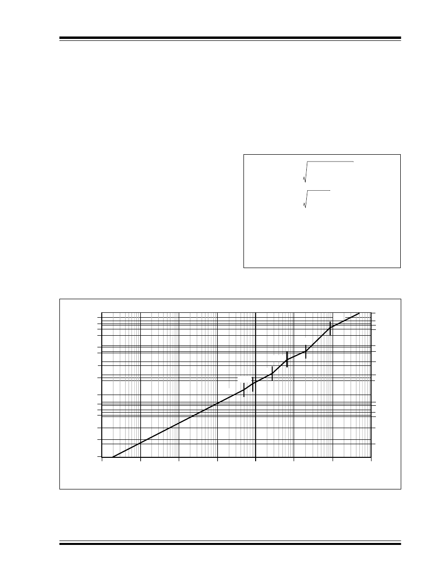
© 2007 Microchip Technology Inc.
DS01114A -page 39
AN1114
Inductor Design
An inductor is a magnetic component that has a single
winding in its core and carries a primarily DC current
along with AC ripple, which is generally very small
compared with DC current. For power inductors, a
toroid is the most commonly used core geometry.
For a power inductor design, two parameters must be
known: the inductance required with the DC bias and
the value of the DC current. The following procedure
defines how to choose the core size and the number of
turns required. The design example is based on the
MPP core selector chart from the manufacturer
MAGNETICS (see Figure 37).
1.
Calculate the energy storage requirement for
the inductor. The data provided by the
manufacturer is L • I
2
; therefore, compute E =
L • I
2
, where L is the inductance value and I is
the DC current flowing through the inductor. For
example, the required inductance of 500 µH for
3 amps DC current would be: E = 4.5 mJ.
2.
Locate the value E in the core selector chart, as
shown in Figure 37. This graph is provided by
the manufacturer. Follow this coordinate to the
intersection with the first core size. Here it
passes through the 125µ section of permeability
and the smallest core that can be used is the
55310 MPP core.
3.
Calculate the number of turns from the AL value,
given by the core manufacturer.
4.
Calculate the magnetic field strength in oersteds
from the magnetic data sheet provided by the
manufacturer.
5.
From the permeability versus DC bias curve,
determine the percentage of initial permeability.
6.
Calculate the actual number of turns required,
based on initial permeability value.
EQUATION 30: INDUCTOR NUMBER OF
TURNS
FIGURE 37:
ENERGY VERSUS CORE SIZE
N
L
REQUIRED
10
6
⋅
A
L
------------------------------------------
=
N
0.5
10
6
90
--------
⋅
=
N
75 turns
=
27.8
125
---------- 75 3
50.04
=
⋅
⋅
N
89
=
55868
55440
55091
55083
55071
55586
55310
55378
55045
55035
55275
55285
55235
55175
55135
0.0001
0.001
0.01
0.1
1
10
100
1000
L
I
2
, mH-amperes
2
Cores
Lis
te
d
by Ge
omet
ry Fa
ct
or
55908
55191
55111
55716
55076
55894
55350
55204
55118
55125
55285
55405
55025
55015
55145
300µ
200µ
160µ
125µ
60µ
26µ
MPP Core Selector Chart
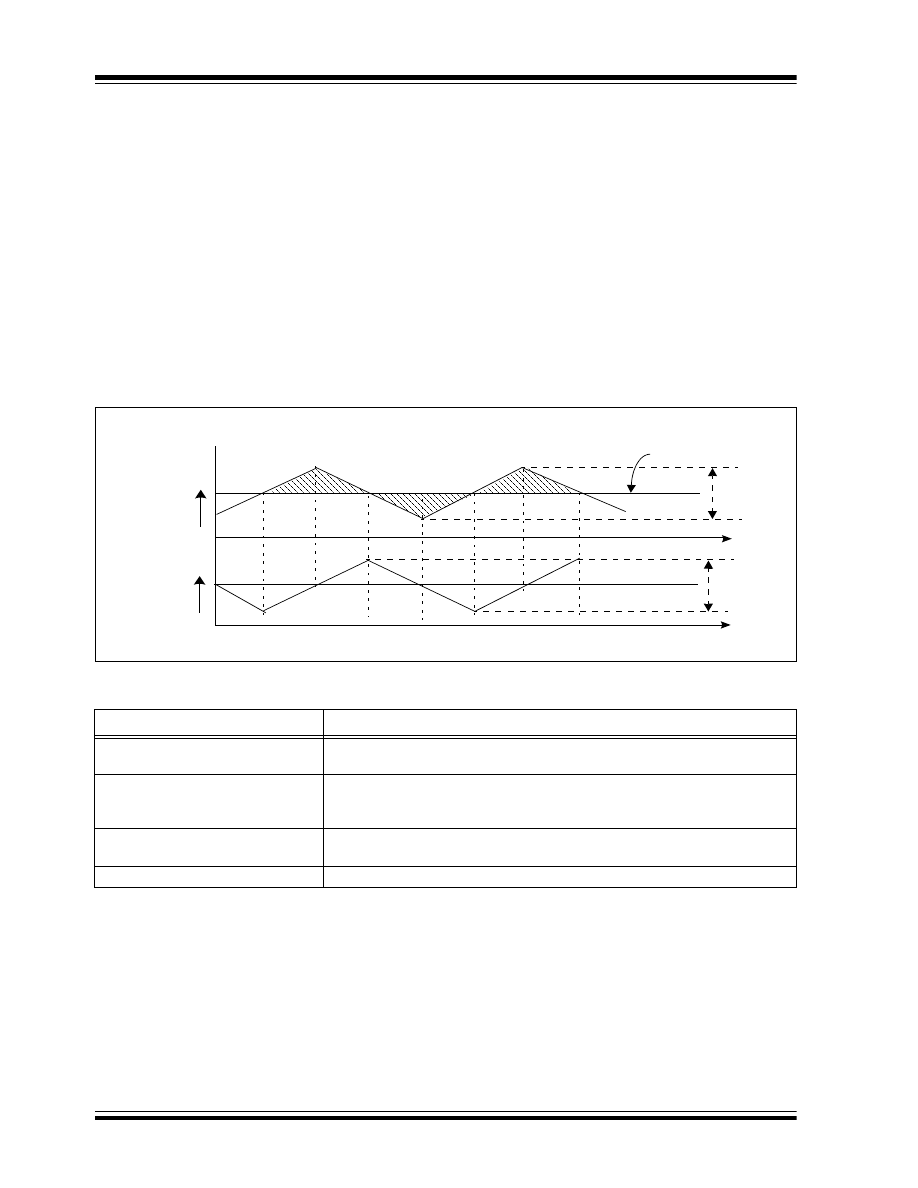
AN1114
DS01114A -page 40
© 2007 Microchip Technology Inc.
Selection of Capacitors
The selection of the input bulk capacitor depends
mainly on the hold-up time required from the power
supply, and the ripple RMS current rating of the
capacitor. Selection of the output capacitor depends on
the maximum operating RMS current, switching
frequency, lifetime and the type of the converter used.
The Equivalent Series Resistor (ESR) of the output
capacitor directly affects the output ripple voltage and
life of the capacitor. Figure 38 shows the current and
voltage waveform across the output capacitor, which
has a
ΔI ripple amplitude centered at the output load
current I
OUT
. The product of
ΔI with the ESR of the
capacitor provides the peak-to-peak ripple voltage
ΔV
at the output voltage.
The life of the capacitor doubles with every 10 degree
drop in temperature from its rated value. For example,
if the capacitor is rated at 5000 hours at 105°C, it would
have a life span of 5000 • 2
4
, which equals 80,000
hours at a 65°C operating temperature.
Table 3 shows the type of capacitors and the
applications where they are typically used.
FIGURE 38:
INDUCTOR CURRENT AND OUTPUT CAPACITOR VOLTAGE WAVEFORM
V
OUT
I
OUT
I
OUT
ΔI
ΔV
TABLE 3:
CAPACITORS AND THEIR CHARACTERISTICS
Type of Capacitor
Typical Application
Aluminum Electrolytic
Generally used at converter input and output where capacitance required is
large and size of the capacitor is not important.
Tantalum
Generally used at output of converter where it requires high ripple current
RMS rating and low ESR of capacitor and size and footprint requirement is
very small. It generally comes in a SMD package.
Ceramic and Multilayer Ceramic
Used for signal and timing application. Used in parallel with electrolytic
capacitor for noise filter.
Film, Polypropylene
Generally used for safety application like X- and Y-type capacitors.

© 2007 Microchip Technology Inc.
DS01114A -page 41
AN1114
ELECTROMAGNETIC
INTERFERENCE (EMI) IN SMPS
One of the biggest challenge faced by a power supply
engineer is to design a power supply that meets the
specification, which calls for EMI and EMC limits. In this
application note, only EMI and more particularly,
practical aspects of EMI are discussed.
There are two types of noise: conducted and radiated.
The most fundamental difference is that the conducted
noise is carried by the conductor and the radiated noise
does not rely on the conductors.
Best Practices
A good PCB layout and good wiring practice drastically
reduces the radiated noise. The high frequency current
loop should be short. A twisted pair of conductors
should be used. A transformer and an inductor with air
gap should be screened to reduce the radiated
magnetic field. The best practice is to keep the line and
return path for any signal as close as possible to each
other, since signal level is directly proportional to the
loop area formed by the signal wires. Also, use metal
for the enclosure box material.
There are two types of conducted noise: the differential
mode noise that flows in one power line and returns on
the other, as shown in Figure 39 (A), and the differential
mode current delivering energy to the load. Common
mode noise flows on both power lines simultaneously,
as shown in Figure 39 (B). Common mode current
does not deliver energy.
FIGURE 39:
COMMON AND
DIFFERENTIAL MODE
NOISE
Place a current probe around both wires to measure
the common mode current in the circuit, as shown in
Figure 40 (A). Now place the power line in the
current probe and make a twist in the returns path,
and then place the current probe to measure the
differential mode current, as shown in Figure 40 (B).
If the common mode current measures 100 µA at
300 kHz, and differential mode current is 1 mA, the
ratio is 1:10. If the total noise voltage measured at
300 kHz is: 101
ΔBµV = 110000 µV = 110 mV, it will
contain 100 mV differential and 10 mV common
mode noise.
FIGURE 40:
MEASUREMENT OF
COMMON AND
DIFFERENTIAL MODE
NOISE
Common Sources of Noise Generation
Figure 41 shows some of the common sources of noise
generation. The conducted electrical noise is mainly
caused by parasitic electrostatic and electromagnetic
coupling between high frequency switching elements
and the ground plane.
The major sources for common mode noise are:
• High
ΔV/Δt switching in the MOSFET
• High-frequency switching transformer
• Output rectifier reverse recovery
The differential noise is suppressed by an input
electrolytic capacitor and a large decoupling capacitor
in parallel with the input bulk capacitor. The common
mode current is introduced to earth ground by
insulation leakage in the transformer and the parasitic
coupling. The maximum value of ground leakage
current (filter capacitor C
Y1
and C
Y2
) that can be placed
is limited by regulatory agencies.
V
IN
V
IN
+
+
Earth
Earth
Noise
Noise
RTN
RTN
(A) Differential mode noise
(B) Common mode noise
V
IN
Current probe
RTN
(B)
V
IN
Current probe
RTN
(A)
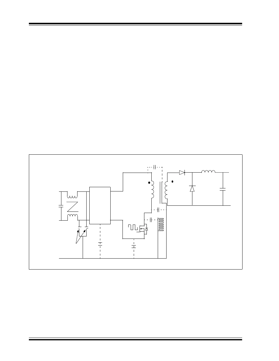
AN1114
DS01114A -page 42
© 2007 Microchip Technology Inc.
NOISE REDUCTION METHODS
The parasitic capacitors, C
P1
through C
P5
, shown in
Figure 41, introduce common mode noise to the
ground line. To reduce noise, the transformer should
have a Faraday screen, which should return to the
input DC line.
The heat sink of the switching device is one of the
major sources of noise. Therefore, an insulating pad
should be used to reduce parasitic capacitance
between the MOSFET and heat sink.
All high voltage components should be isolated from
the ground plane.
To minimize the EMI filter inductor size, the largest
decoupling capacitor value should be used.
To reduce noise generated due to high
ΔV/Δt and
ΔI/Δt, a snubber circuit is sometimes added in
parallel across the switching device.
A high permeability core is used for a common mode
inductor to provide high common mode inductance, as
well as carry the line input current in the smallest core.
The winding of a common mode inductor is physically
separated, and a bobbin with two isolation sections is
used to meet safety requirements and to have leakage
inductance between the two windings. This leakage
inductance will help in suppressing differential noise.
The self-resonant frequency of the common mode
inductor should be as high as possible to maintain good
high frequency rejection. To meet this, interwinding
capacitance should be as low as possible. For this
reason, a high permeability ferrite toroidal core with a
single layer can be used to avoid interwinding
capacitance, and having a one or two turn difference in
the two windings to create leakage inductance to
differential noise.
To know what value of inductor to start with, measure
the value of the largest noise voltage in the system with
only a filter capacitor present, and then decide the
value of the inductor required to bring it down to an
acceptable limit at that frequency. The losses in the
common inductor will be only copper loss, as the core
inductor and skin effect are negligible.
FIGURE 41:
SOURCE OF COMMON AND DIFFERENTIAL MODE NOISE
X-capacitor
C
Y1
C
Y2
C
P3
C
P5
Diode
Bridge
Y-capacitor
C
P4
C
P2
C
P1

© 2007 Microchip Technology Inc.
DS01114A -page 43
AN1114
SUMMARY
The appropriate SMPS topology can be selected based
on input voltage, output power, and output current (see
Table 4).
The selection of topology may differ to meet some of
the specific requirements of the power supply including
cost, size and personal experience of the designer.
TABLE 4:
SMPS TOPOLOGY SELECTION GUIDELINES
Input voltage
Output power
Preferred Topology
Universal input (90-264) V
AC
Po < 150 watt, Load current < 10A Flyback, Forward
Universal input (90-264) V
AC
Po < 150 watt, Load current > 10A Forward
Universal input (90-264) V
AC
150 watt < Po > 350
Two-Switch Forward, Half-Bridge, Push-Pull
Universal input (90-264) V
AC
Po < 500 watt
Half-Bridge, Push-Pull
Vin > 350 VDC
Po < 750 watt
Half-Bridge
Vin < 200 VDC
Po < 500 watt
Push-Pull
Vin > 350 VDC
500 < Po > 1000 watt
Full-Bridge
Vin > 350 VDC
Po > 1000 watt
ZVT Full-Bridge
Vin > 350 VDC
Po > 2000 watt
More than one ZVT full-bridge in parallel,
interleaved with more than one ZVT full-bridge

AN1114
DS01114A -page 44
© 2007 Microchip Technology Inc.
APPENDIX A: GLOSSARY
Bipolar Junction Transistor (BJT)
A BJT is a three-terminal device constructed of doped
semiconductor material and may be used in amplifying
or switching applications.
Boost Converter
A basic SMPS topology in which energy is stored in a
inductor when a switch is ON, and is transferred to the
output when the switch is OFF. It converts an
unregulated input voltage to a regulated output voltage
higher than the input.
Buck Converter
A basic SMPS topology in which a series switch chops
the input voltage and applies the pulses to an
averaging LC filter, which produces a lower output
voltage than the input.
Constant Output Voltage
A mode of operation when output voltage is regulated
regardless of any other parameter changes in the
system.
Current Mode Control
A control method which is using a dual loop circuit to
adjust the PWM operation.
Electromagnetic Interference (EMI)
Unwanted energy, in the form of electrical noise
generated from the SMPS, which may be conducted or
radiated.
Faraday Shield
An electrostatic shield between input and output
windings of a transformer. This is used to reduce
primary to secondary coupling capacitance, which in
turn will reduce output common mode noise.
Feed Forward
A term describing a system that reacts to changes in its
environment, usually to maintain some desired state of
the system. Also, it is a system that exhibits
feed-forward behavior that responds to a measured
disturbance in a predefined way, in contrast with a
feedback system.
Flyback Converter (FBT)
An isolated Buck-Boost SMPS topology in which,
during the first period of a switching cycle, the energy
is stored in a magnetizing inductance of the
transformer. Then, during the second period, this
energy is transferred to a secondary winding of the
same half-bridge resonant converter where the load is
connected in series with the resonant tank capacitor, C,
and into the load.
Forward Converter
A Buck-derived SMPS topology in which energy is
transferred to the secondary of a transformer winding
and into the load, when the switching transistor is ON.
Full-Bridge Converter
An SMPS topology in which four switches are
connected in a bridge configuration to drive the primary
of a transformer. This is also known as an H-Bridge
Converter.
H-Bridge Converter
See Full-Bridge Converter.
Half-Bridge Converter
A SMPS topology similar to a full-bridge converter in
which only two switches are used. The other two are
replaced by capacitors.
Half-Bridge LLC Resonant Converter
A SMPS half-bridge topology where the series
resonant tank consisting of the inductor, L, and the
capacitor, C, which is used to generate another
resonant frequency with transformer magnetizing
inductance.
Half-Bridge Resonant Converter
A half-bridge converter using an LC resonant tank to
reduce the switching losses in the MOSFET.
H-Bridge Phase-Shift ZVT Converter
A full-bridge converter using the phase-shift ZVS
technique is known as an H-Bridge Phase-Shift ZVT
topology. In this topology, the parasitic output capacitor
of the MOSFETs and the leakage inductance of the
switching transformer are used as a resonant tank
circuit to achieve zero voltage across the MOSFET at
the turn-on transition.

© 2007 Microchip Technology Inc.
DS01114A -page 45
AN1114
LLC Resonant Converter
A full-bridge converter with an LC resonant tank, which
is used to reduce switching losses and the phase shift
between the two leg gate pulse defined in the output
power flow.
Parallel Resonant Converter (PRC)
A half-bridge resonant converter where the load is
connected in parallel with the resonant tank capacitor, C.
Power Diode
A power diode is a unidirectional semiconductor switch,
which has only one PN junction. A power diode is able
to carry a large amount of current and typically is able
to support a large reverse-bias voltage in the OFF
state.
Power Factor Correction (PFC)
PFC is a technique of counteracting the undesirable
effects of electric loads that create a power factor that
is less than 1.
Push-Pull Converter
An SMPS topology which is using usually a center-tap
transformer and two switches that are driven ON and
OFF alternately.
Series Resonant Converter (SRC)
A half-bridge resonant converter where the load is
connected in series with the resonant tank capacitor, C.
Snubber
A component or a circuit, active or passive, dissipative
or regenerative used in a SMPS to reduce components
stress by limiting peak voltage or current,
ΔV/Δt, ΔI/Δt.
Switch Mode Power Supply (SMPS)
A power supply technology in which a switching device,
along with a passive component, is used to process the
power flow.
Total Harmonic Distortion (THD)
The total harmonic distortion or THD, of a signal is a
measurement of the harmonic distortion present and is
defined as the ratio of the sum of the powers of all
harmonic components to the power of the fundamental.
Two-Switch Forward Converter
Used in series with the transformer primary to reduce
the reverse blocking voltage of the switch.
Voltage Mode Control
A control method that uses a single loop to control the
output.

AN1114
DS01114A -page 46
© 2007 Microchip Technology Inc.
NOTES:

© 2007 Microchip Technology Inc.
DS01114A -page 47
Information contained in this publication regarding device
applications and the like is provided only for your convenience
and may be superseded by updates. It is your responsibility to
ensure that your application meets with your specifications.
MICROCHIP MAKES NO REPRESENTATIONS OR
WARRANTIES OF ANY KIND WHETHER EXPRESS OR
IMPLIED, WRITTEN OR ORAL, STATUTORY OR
OTHERWISE, RELATED TO THE INFORMATION,
INCLUDING BUT NOT LIMITED TO ITS CONDITION,
QUALITY, PERFORMANCE, MERCHANTABILITY OR
FITNESS FOR PURPOSE. Microchip disclaims all liability
arising from this information and its use. Use of Microchip
devices in life support and/or safety applications is entirely at
the buyer’s risk, and the buyer agrees to defend, indemnify and
hold harmless Microchip from any and all damages, claims,
suits, or expenses resulting from such use. No licenses are
conveyed, implicitly or otherwise, under any Microchip
intellectual property rights.
Trademarks
The Microchip name and logo, the Microchip logo, Accuron,
dsPIC, K
EE
L
OQ
, K
EE
L
OQ
logo, microID, MPLAB, PIC,
PICmicro, PICSTART, PRO MATE, rfPIC and SmartShunt
are registered trademarks of Microchip Technology
Incorporated in the U.S.A. and other countries.
AmpLab, FilterLab, Linear Active Thermistor, Migratable
Memory, MXDEV, MXLAB, SEEVAL, SmartSensor and The
Embedded Control Solutions Company are registered
trademarks of Microchip Technology Incorporated in the
U.S.A.
Analog-for-the-Digital Age, Application Maestro, CodeGuard,
dsPICDEM, dsPICDEM.net, dsPICworks, dsSPEAK, ECAN,
ECONOMONITOR, FanSense, FlexROM, fuzzyLAB,
In-Circuit Serial Programming, ICSP, ICEPIC, Mindi, MiWi,
MPASM, MPLAB Certified logo, MPLIB, MPLINK, PICkit,
PICDEM, PICDEM.net, PICLAB, PICtail, PowerCal,
PowerInfo, PowerMate, PowerTool, REAL ICE, rfLAB, Select
Mode, Smart Serial, SmartTel, Total Endurance, UNI/O,
WiperLock and ZENA are trademarks of Microchip
Technology Incorporated in the U.S.A. and other countries.
SQTP is a service mark of Microchip Technology Incorporated
in the U.S.A.
All other trademarks mentioned herein are property of their
respective companies.
© 2007, Microchip Technology Incorporated, Printed in the
U.S.A., All Rights Reserved.
Printed on recycled paper.
Note the following details of the code protection feature on Microchip devices:
•
Microchip products meet the specification contained in their particular Microchip Data Sheet.
•
Microchip believes that its family of products is one of the most secure families of its kind on the market today, when used in the
intended manner and under normal conditions.
•
There are dishonest and possibly illegal methods used to breach the code protection feature. All of these methods, to our
knowledge, require using the Microchip products in a manner outside the operating specifications contained in Microchip’s Data
Sheets. Most likely, the person doing so is engaged in theft of intellectual property.
•
Microchip is willing to work with the customer who is concerned about the integrity of their code.
•
Neither Microchip nor any other semiconductor manufacturer can guarantee the security of their code. Code protection does not
mean that we are guaranteeing the product as “unbreakable.”
Code protection is constantly evolving. We at Microchip are committed to continuously improving the code protection features of our
products. Attempts to break Microchip’s code protection feature may be a violation of the Digital Millennium Copyright Act. If such acts
allow unauthorized access to your software or other copyrighted work, you may have a right to sue for relief under that Act.
Microchip received ISO/TS-16949:2002 certification for its worldwide
headquarters, design and wafer fabrication facilities in Chandler and
Tempe, Arizona; Gresham, Oregon and design centers in California
and India. The Company’s quality system processes and procedures
are for its PIC
®
MCUs and dsPIC
®
DSCs, K
EE
L
OQ
®
code hopping
devices, Serial EEPROMs, microperipherals, nonvolatile memory and
analog products. In addition, Microchip’s quality system for the design
and manufacture of development systems is ISO 9001:2000 certified.

DS01114A -page 48
© 2007 Microchip Technology Inc.
AMERICAS
Corporate Office
2355 West Chandler Blvd.
Chandler, AZ 85224-6199
Tel: 480-792-7200
Fax: 480-792-7277
Technical Support:
http://support.microchip.com
Web Address:
www.microchip.com
Atlanta
Duluth, GA
Tel: 678-957-9614
Fax: 678-957-1455
Boston
Westborough, MA
Tel: 774-760-0087
Fax: 774-760-0088
Chicago
Itasca, IL
Tel: 630-285-0071
Fax: 630-285-0075
Dallas
Addison, TX
Tel: 972-818-7423
Fax: 972-818-2924
Detroit
Farmington Hills, MI
Tel: 248-538-2250
Fax: 248-538-2260
Kokomo
Kokomo, IN
Tel: 765-864-8360
Fax: 765-864-8387
Los Angeles
Mission Viejo, CA
Tel: 949-462-9523
Fax: 949-462-9608
Santa Clara
Santa Clara, CA
Tel: 408-961-6444
Fax: 408-961-6445
Toronto
Mississauga, Ontario,
Canada
Tel: 905-673-0699
Fax: 905-673-6509
ASIA/PACIFIC
Asia Pacific Office
Suites 3707-14, 37th Floor
Tower 6, The Gateway
Harbour City, Kowloon
Hong Kong
Tel: 852-2401-1200
Fax: 852-2401-3431
Australia - Sydney
Tel: 61-2-9868-6733
Fax: 61-2-9868-6755
China - Beijing
Tel: 86-10-8528-2100
Fax: 86-10-8528-2104
China - Chengdu
Tel: 86-28-8665-5511
Fax: 86-28-8665-7889
China - Fuzhou
Tel: 86-591-8750-3506
Fax: 86-591-8750-3521
China - Hong Kong SAR
Tel: 852-2401-1200
Fax: 852-2401-3431
China - Nanjing
Tel: 86-25-8473-2460
Fax: 86-25-8473-2470
China - Qingdao
Tel: 86-532-8502-7355
Fax: 86-532-8502-7205
China - Shanghai
Tel: 86-21-5407-5533
Fax: 86-21-5407-5066
China - Shenyang
Tel: 86-24-2334-2829
Fax: 86-24-2334-2393
China - Shenzhen
Tel: 86-755-8203-2660
Fax: 86-755-8203-1760
China - Shunde
Tel: 86-757-2839-5507
Fax: 86-757-2839-5571
China - Wuhan
Tel: 86-27-5980-5300
Fax: 86-27-5980-5118
China - Xian
Tel: 86-29-8833-7252
Fax: 86-29-8833-7256
ASIA/PACIFIC
India - Bangalore
Tel: 91-80-4182-8400
Fax: 91-80-4182-8422
India - New Delhi
Tel: 91-11-4160-8631
Fax: 91-11-4160-8632
India - Pune
Tel: 91-20-2566-1512
Fax: 91-20-2566-1513
Japan - Yokohama
Tel: 81-45-471- 6166
Fax: 81-45-471-6122
Korea - Daegu
Tel: 82-53-744-4301
Fax: 82-53-744-4302
Korea - Seoul
Tel: 82-2-554-7200
Fax: 82-2-558-5932 or
82-2-558-5934
Malaysia - Kuala Lumpur
Tel: 60-3-6201-9857
Fax: 60-3-6201-9859
Malaysia - Penang
Tel: 60-4-646-8870
Fax: 60-4-646-5086
Philippines - Manila
Tel: 63-2-634-9065
Fax: 63-2-634-9069
Singapore
Tel: 65-6334-8870
Fax: 65-6334-8850
Taiwan - Hsin Chu
Tel: 886-3-572-9526
Fax: 886-3-572-6459
Taiwan - Kaohsiung
Tel: 886-7-536-4818
Fax: 886-7-536-4803
Taiwan - Taipei
Tel: 886-2-2500-6610
Fax: 886-2-2508-0102
Thailand - Bangkok
Tel: 66-2-694-1351
Fax: 66-2-694-1350
EUROPE
Austria - Wels
Tel: 43-7242-2244-39
Fax: 43-7242-2244-393
Denmark - Copenhagen
Tel: 45-4450-2828
Fax: 45-4485-2829
France - Paris
Tel: 33-1-69-53-63-20
Fax: 33-1-69-30-90-79
Germany - Munich
Tel: 49-89-627-144-0
Fax: 49-89-627-144-44
Italy - Milan
Tel: 39-0331-742611
Fax: 39-0331-466781
Netherlands - Drunen
Tel: 31-416-690399
Fax: 31-416-690340
Spain - Madrid
Tel: 34-91-708-08-90
Fax: 34-91-708-08-91
UK - Wokingham
Tel: 44-118-921-5869
Fax: 44-118-921-5820
W
ORLDWIDE
S
ALES
AND
S
ERVICE
09/10/07
Document Outline
- Introduction
- Why SMPS?
- Selection of SMPS Topologies
- Buck Converter
- Boost Converter
- Forward Converter
- Two-Switch Forward Converter
- Flyback Converter (FBT)
- Push-Pull Converter
- Half-Bridge Converter
- Half-Bridge Resonant Converter
- FIGURE 18: series resonant converter
- FIGURE 19: DC Characteristics
- FIGURE 20: Current and Voltage Waveform
- FIGURE 21: Parallel Resonant Converter
- FIGURE 22: DC Characteristics
- FIGURE 23: Current and Voltage Wave Form
- FIGURE 24: Half-Bridge LLC Resonant Converter
- EQUATION 18: LLC RESONANT Frequencies
- FIGURE 25: DC Characteristic of LLC Resonant Converter
- FIGURE 26: LLC Resonant Converter
- Full-Bridge Converter
- Method of Control
- Magnetics Design
- Electromagnetic Interference (EMI) in SMPS
- Summary
- Appendix A: Glossary
- Bipolar Junction Transistor (BJT)
- Boost Converter
- Buck Converter
- Constant Output Voltage
- Current Mode Control
- Electromagnetic Interference (EMI)
- Faraday Shield
- Feed Forward
- Flyback Converter (FBT)
- Forward Converter
- Full-Bridge Converter
- H-Bridge Converter
- Half-Bridge Converter
- Half-Bridge LLC Resonant Converter
- Half-Bridge Resonant Converter
- H-Bridge Phase-Shift ZVT Converter
- LLC Resonant Converter
- Parallel Resonant Converter (PRC)
- Power Diode
- Power Factor Correction (PFC)
- Push-Pull Converter
- Series Resonant Converter (SRC)
- Snubber
- Switch Mode Power Supply (SMPS)
- Total Harmonic Distortion (THD)
- Two-Switch Forward Converter
- Voltage Mode Control
Wyszukiwarka
Podobne podstrony:
A 12kw Switching Mode Power Supply With Free Input Voltage
DESIGN OF A SWITCHING MODE POWER SUPPLY WITH UPS FEATURES
17V 10A Switch Mode Power Supply (PCB layout) 020054 3
SI 8033JD, SI 8050JD, SI 8090JD Surface Mount, Separate Excitation Switching Type Power Supply ICes
SWITCHING POWER SUPPLY DESIGN CONTINUOUS MODE FLYBACK CONVERTER
(Wydruk – ATX Switching Power Supply 13,8 V Proste zmiany w celu zwiększenia napięcia wyjściowego Ja
300W, 300Khz Current Mode Half Bridge Power Supply With Multiple Outputs Using Coupled Inductors
Power MOS FET in Switching Power Supply
Power Supply Topologies
Layout guidlines for switching power supply
Switching Power Supply Tutorial
Digital Control Of Switching Power Supply Power Factor Correction Stage
Switching Power Supply 2
Convert Computer ATX Power Supply to Lab Power Supply
Jvc Power Supply Description And Trouble Shooting Procedure
Battery Inverter For Modularly Structured Pv Power Supply Systems
0 50V 2A LM10C, 0 50V 2A Bench power supply circuit diagrams, schematics, electronic projects
więcej podobnych podstron