
F. Sherman, S. Tung, C-J. Kim, C-M Ho, and J. Woo
1
Flow Control by Using High-Aspect-Ratio, In-plane
Microactuators
Faiz Sherman, Steve Tung**, Chang-Jin “CJ” Kim, Chih-Ming Ho, and Jason Woo
*
Mechanical and Aerospace Engineering Department
*
Electrical Engineering Department
University of California, Los Angeles,
Los Angeles, CA 90095-1597, U.S.A. (E-mail: cjkim@seas.ucla.edu)
**Presently with Litton Guidance and Control Systems
5500 Canoga, Woodland Hills, CA 91367

F. Sherman, S. Tung, C-J. Kim, C-M Ho, and J. Woo
2
ABSTRACT
The successful design, modeling, fabrication, and testing of high-aspect-ratio large deflection in-
plane microactuators are presented. The large displacement, in-plane actuator has a unique
application in the area of fluid flow control. Unlike previously used electromagnetically actuated
microflap in which motion was normal to the substrate, we introduce a novel design that alters the
local fluid flow by moving the actuators parallel to the substrate. This new approach of “in-plane
motion” allows for a condition free of “form drag.” Furthermore, electrostatic drive allows for
lower power consumption (
µW). The actuator includes microplates that are 60 µm X 200 µm.
These microplates, when moved parallel to the substrate surface, induces a “spanwise velocity”
into the flow field above them. This induced velocity field, when applied to the near-wall streaks
(regions of high shear drag), would increase the transport of high-speed fluid away from the wall,
therefore causing reduction in viscous drag. The actuators are made from silicon-on-insulator
(SOI) wafers using a one mask deep reactive-ion-etching (DRIE) process. The microplates are
suspended by a high-aspect-ratio cantilever structure (2
µm wide, 6-18 µm thick silicon) to ensure
robustness against any disturbances in the out-of-plane direction. We present experimental
verification of both the induced Stoke’s flow and a local fluid flow created by our in-plane
microactuators.
Key words: Silicon-on-insulator, high aspect ratio, deep reactive ion etching, viscous drag
reduction, in-plane actuator, large deflection

F. Sherman, S. Tung, C-J. Kim, C-M Ho, and J. Woo
3
INTRODUCTION
Conventional techniques for active control of fluid flow consist of changing the skin friction by wall motion, heating
and cooling the wall, and injecting mass. These techniques are all being implemented in macroscale [1]. However,
they suffer from severe limitation in the areas of spatial resolution, operational frequency of the actuator, and the
power consumption. It therefore becomes apparent that MEMS actuators offer a very attractive solution for active
control of fluid flow [2]. The inherent nature of MEMS devices offers excellent spatial resolution and high operational
frequency with low power consumption.
Recently published work on magnetically actuated microflaps moving in the out-of-plane direction has shown the
feasibilty of active control of “streaks” (high speed fluid approaching the wall region) in microscale [2-5]. The control
was done by displacing a microflap in the out-of–plane direction so as to produce an upward velocity against the
streaks. This induced velocity field counteracts a streak, thereby reducing the viscous drag caused by the high speed
fluid. The size of the microflaps used was of millimeter scale and magnetically driven. The operational frequency is
thus limited (~100 Hz), and the power consumption was relatively high (mW).
The goal of this paper is to realize the induction of a local fluid flow caused by in-plane actuation of an array of
electrostatically driven microdevices. Modeling results have indicated that the induced local fluid flow due to the in-
plane actuators can eventually serve to reduce viscous drag. The devices are made flush to the substrate and operate in
the in-plane direction to be free from “form drag” (drag induced due to a physical presence of an object obstructing a
flow). This is in contrast to the microflaps [4]. The reported in-plane microactuators are electrostatically driven and
are approximately 10 times smaller than the magnetic microflap actuator, allowing for low power consumption (< 1
µ
W) and high operating frequency (500-1000 Hz).

F. Sherman, S. Tung, C-J. Kim, C-M Ho, and J. Woo
4
THEORY AND MODELING
Flow Theory
Generally, the presence of a counter-rotating vortex pair gives rise to a region of high viscous drag, Fig. 1. These
occurrences are known as “streaks”. Streaks bring in high speed fluid downward to the wall region increasing drag.
It is expected that the viscous wall drag will be reduced if an upward flow is induced to counteract this downward
motion of the high speed flow.
The physical sizes of the streaks are a function of Reynolds number. For this paper we choose a Reynolds number that
is 10,000 (a parameter value similar to test conditions of the magnetic microflap [3]). With a Reynolds number of
10,000 the streaks have an average width of 900
µ
m and an average length of 30 mm. These physical feature sizes of
the streaks dictate the design criteria of the microdevice. With such values of streak width and length, three criteria
for the in-plane microactuator are required. The first is that the actuator end plates be as long as possible in order to
interact with as much of the streak (from their length point of view). Secondly, the actuators should produce large
enough plate displacement in order to affect the streaks (from their width point of view); otherwise, they would not
have an effect on the streaks. Thirdly, the induced flow velocity must be large enough to interfere with the down flow
of the incoming high speed fluid. The last condition dictates the actuators operate at relatively high frequency (~1
kHz).
An important parameter obtained from a previous modeling effort [6] and data from the magnetic microflap actuator
[3] suggest an induced velocity on the order of 1-10 cm/s to be sufficient to cause substantial reduction in viscous drag
(> 20%). To satisfy the criteria imposed by the flow conditions, our actuators are made to move long microplates (200
µ
m long) a distance over 100
µ
m with high operating frequency (0.5–1.2 kHz) and low power requirements (nW).
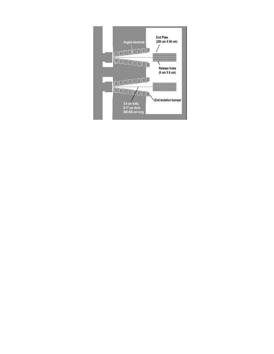
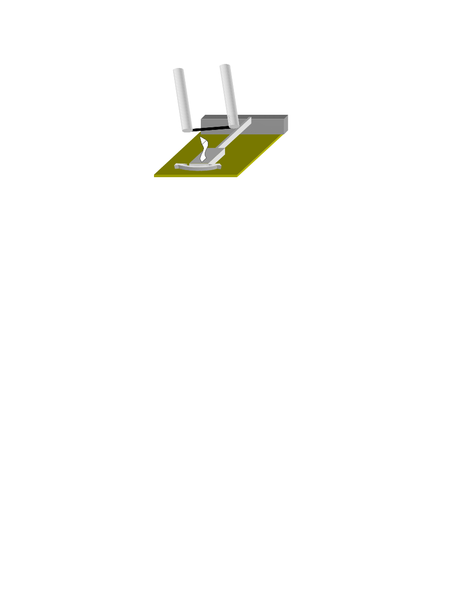
Design of the Actuator

F. Sherman, S. Tung, C-J. Kim, C-M Ho, and J. Woo
5
The actuators consist of large microplates (60
µ
m wide, 200
µ
m long) attached at the end of long cantilever beams
(500-800
µ
m), see Fig. 2. The cantilever beams are electrostatically driven using angled electrodes [7,8]. Isolation
bumpers (40
µ
m X 40
µ
m) are embedded within these electrodes to prevent shorting between the cantilever beams and
driving electrodes. The size of the bumpers are designed to be large enough to allow for a timed release of the
actuators while still ensuring good anchor to the substrate. The length of the supporting cantilever beams range from
500 to 800
µ
m and width and thickness range from 2-4
µ
m and 6-18
µ
m, respectively. These dimensions constitute a
high-aspect ratio device that is rigid in the out-of-plane direction and yet flexible in the in-plane direction. The
microplates have within them 6
µ
m X 6
µ
m etch holes to control the HF etching time for release process. The
actuators are configured in an array format in pair formation as shown in Fig. 2. This pair formation allows for
maximum induction of fluid flow. They are also designed to be in a recessed area so that the top surface of the plates
and the electrodes are on the same plane as the substrate surface (wall) to prevent any interference on the oncoming
fluid.
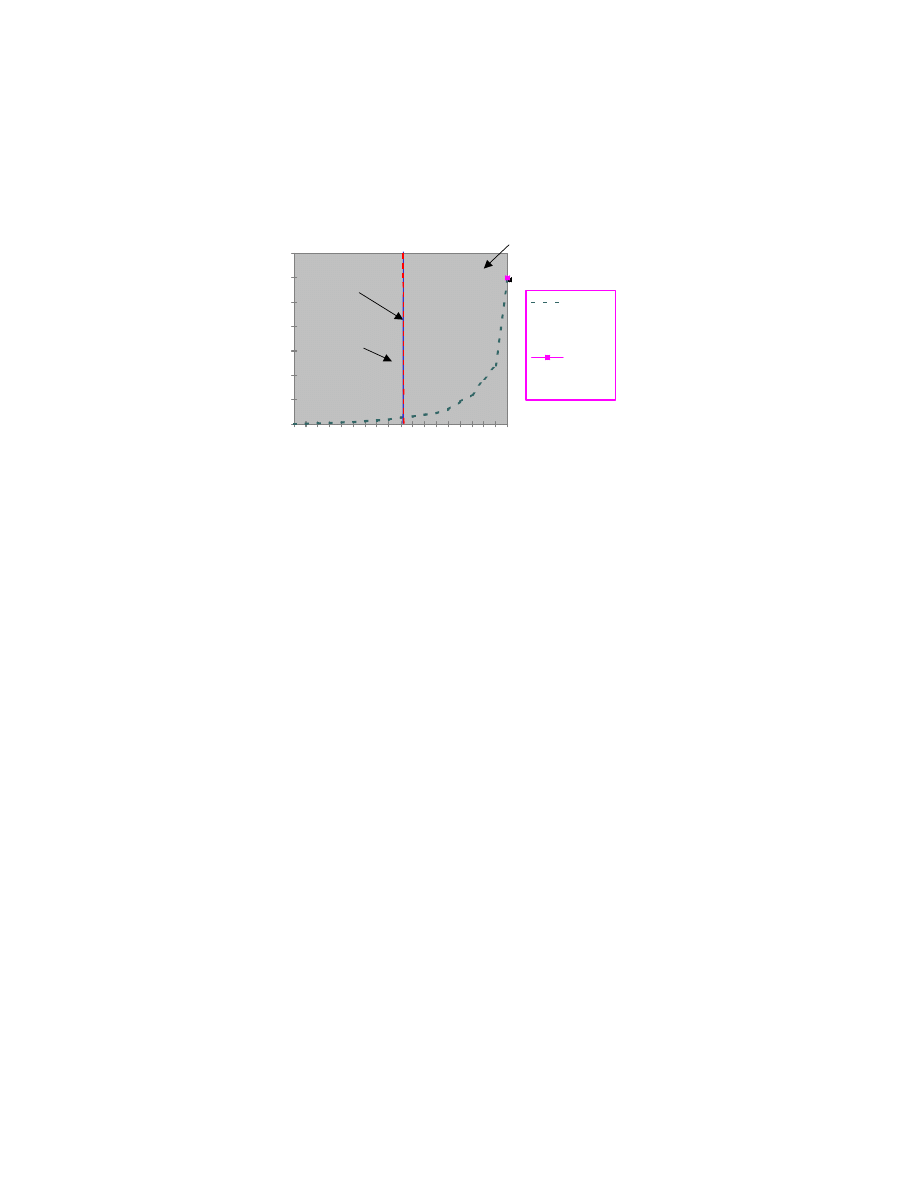
Modeling of the Actuator
Electrostatic performance, resonance modes, and frequencies require rigorous analysis due to the fact that our
actuators are operated under large deflection and high frequency conditions. An understanding of the effect of the
large end plate on the dynamic response of the actuators is also necessary for the successful operation of the actuators.
Electrostatic modeling was performed via the coupling of a commercial finite element software (ANSYS) and a
Fortran program. The material properties used for the modeling are: Young’s modulus of 180 GPa, density of 2330
kg/m
3
, and Poisson’s ratio of 0.27. Our modeling effort was compared with both previous experimental data [7] and
data that was obtained by our in-plane actuators. Fig. 3 shows merit of predictability of our model with respect to the
data.

F. Sherman, S. Tung, C-J. Kim, C-M Ho, and J. Woo
6
Finite element model using ANSYS is done to determine the dynamic response of the cantilever-plate system. Both a
modal analysis and a harmonic response analysis are performed for the case of a 4
µ
m wide, 18
µ
m thick, and 500
µ
m
long actuator with an end plate that is 60
µ
m wide and 200
µ
m long. Fig. 4(a) shows the first resonance mode of the
actuator, occurring at 2.5 kHz. Up to the actuator’s fundamental frequency, the end plate follows the beam without
any relative rotation to the cantilever tip and does not attenuate the amplitude. The second mode of the device is in the
out-of-plane direction, Fig. 4(b), at 6.2 kHz. The third mode occurs at 34.7 kHz. At this mode, the rotational effect of
the end plate keeps the overall in-plane motion of the end plate almost stationary, Fig. 4(c).
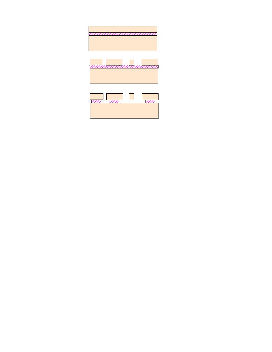
FABRICATION
Fabrication of the in-plane microactuators is done on commercially available, custom-ordered, Silicon-On-Insulator
(SOI) wafers (a sandwich structure that consists of Silicon/Oxide/Silicon). The wafers had to meet three constraints
imposed on them; a certain level of conductivity, thickness of sacrificial oxide, and the thickness of the top silicon.
First, the high conductivity is required in order to have both a driving signal on the top silicon and a ground potential
on the bottom silicon carried without metalization. Therefore the wafers needed to be heavily doped on both the
handle wafer (i.e., the main substrate) and the device wafer (i.e., top layer). Second, the thickness of sacrificial oxide
on the SOI wafer needs to be thick such that the cantilever and end plates are released, safety bumpers anchored, and
the gap large enough to ensure long travel over the substrate during operation. Electrical breakdown through the
oxide layer under high actuation voltage is yet another consideration. We used 3
µ
m thick oxide. Third, we varied the
thickness of the top silicon (device layer) from 6
µ
m to 18
µ
m in order to fabricate high-aspect-ratio structures with
narrow beam width (as small as 2
µ
m).

F. Sherman, S. Tung, C-J. Kim, C-M Ho, and J. Woo
7
The fabrication consists of a single mask and three processing steps. We begin by using a Bond and Etch Back
Silicon-On-Insulator (BESOI) wafer, Fig. 5 (a). The SOI wafer is made from two highly doped (100) 4 inch wafers
(0.005
Ω
.cm). Wet oxide of 1.5
µ
m is grown on each wafer, and the wafers are then bonded, oxide to oxide, at room
temperature. They are then placed in an 800
0
C furnace to strengthen the bond. On completion of the annealing, one
side of the bonded wafer undergoes grinding to the target device thickness. Once the target thickness is reached, the
wafers are polished to give a finished surface.
After photoresist is patterned to define the device, the wafers are sent to MCNC [9] for a deep reactive-ion etch (DRIE)
which is performed through the device layer to the sacrificial oxide, Fig. 5(b). To account for non-uniformity across
the wafer, a 15% over etch was used in combination with an end-point detection system. The photoresist is then
stripped in-house and the wafers are diced to 1 cm X 1 cm dies which are used for actual flow experiments. Finally,
the test chips undergo a release process, Fig 5(c).
The release process is a timed etch of the sacrificial oxide. The
oxide underneath the actuators is removed in 8 minutes of 49% HF. All the other structures have significantly larger
anchor areas, therefore allowing them to remain anchored after the cantilevers and end plates have been released.
Releasing/drying was a challenge, despite the thickness of the beam (over 10 µm), due to the length (up to 1000
µ
m
overall) and the existence of large plates at the end. The standard CO
2
supercritical drying [10] and surface
passivation by self-assembled monolayer (SAM) coating (Octadecyl Trichloro Silane) [11,12], both proven effective
for simple beams [13], produced a dismal result (< 10% yield) for the in-plane microactuators. For the CO
2
drying, it
is speculated that the difficulty stemmed from replacing the methanol under the large plates with the CO
2
liquid
through the narrow and deep trenches made by DRIE. Similar problems also make the SAM coating method
ineffective.
A dramatic improvement has been found for the CO
2
drying when the chip was loaded “upside down” on completion
of the methanol soak, apparently helping the methanol drip by gravity in lighter CO
2
liquid. Rinsing times are also
increased to provide longer time for diffusion. The release process consists of 8 min in 49% HF followed by 30
minutes deionized (DI) water rinse in three successive baths (10 minutes each). The chips are then transferred to

F. Sherman, S. Tung, C-J. Kim, C-M Ho, and J. Woo
8
methanol and kept for yet another 30 minutes before CO
2
drying. Twenty CO
2
rinses are done with a dwelling time of
3 minutes in between each rinse. This release method provided a success close to 100% yield.
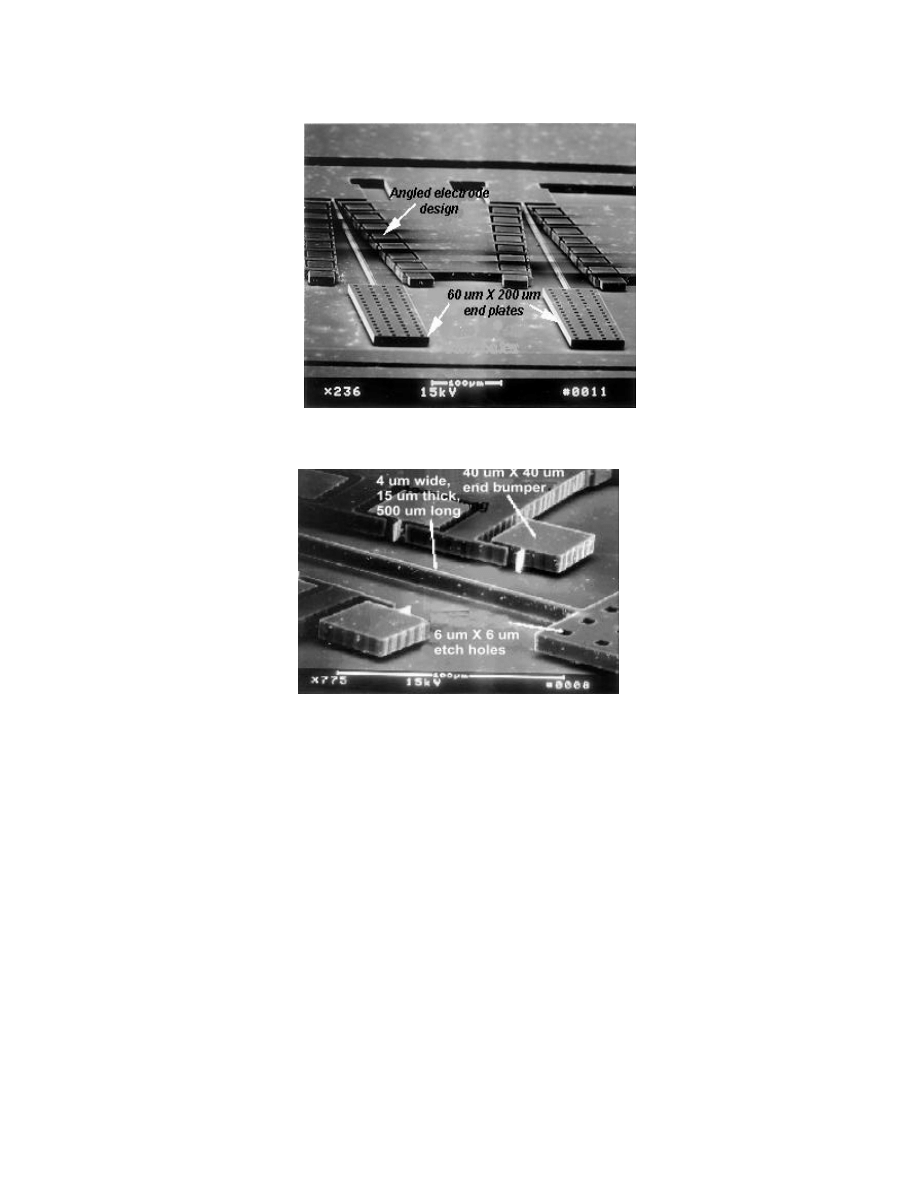
Fig. 6 (a) shows a pair of the recessed released actuator with the angled electrode configuration used to drive it. The
recess serves a function of preventing any unwanted effects on the on-coming fluid flow. In addition, this design type
shields the actuators against any perturbation in the flow that might cause the devices to break off. Fig. 6 (b) is the
close-up showing the high-aspect-ratio beam, the end plate, release holes on it, angled drive electrodes, and
electrostatic isolation bumpers.
TESTING
The two goals of this work were to verify Stoke’s flow and net induced local flow in the direction opposite to the flow
being brought in by a vortex pair. Verification of Stoke’s flow was done by standard micro hot-wire, while that of the
induced flow was done by a flow visualization technique.
To verify Stoke’s flow, a hot-wire anemometer is placed 400
µ
m above the microactuator’s end plate, Fig. 7. The hot-
wire is turned on and a signal is recorded before activating the actuator. Then the actuator is turned on and made to
displace the end plate 100
µ
m peak-to-peak at a frequency of 500 Hz. While the signal from the hot-wire is being
recorded, the actuator is turned off again, Fig. 8. Fig. 8 clearly indicates that the signal obtained from the hot-wire is
that of the induced Stoke’s flow following the frequency of the actuator.
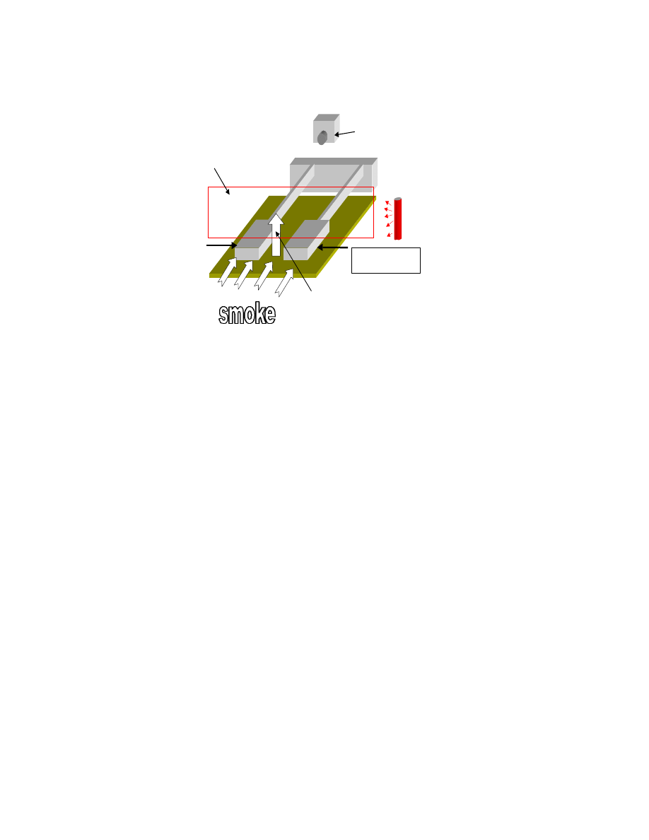
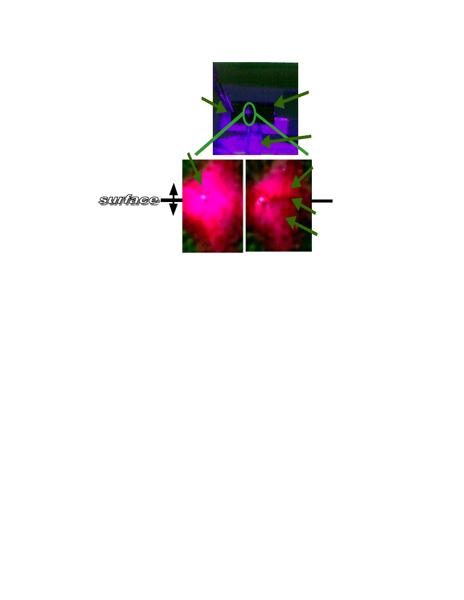
In the second experiment, a smoke generator introduces smoke onto a pair of actuators. A laser sheet shining through
the smoke is placed on top of the actuators, Fig. 9. The entire experiment is enclosed in a controlled environment that
allows for stagnant fluid. Once the smoke is introduced onto the actuators, it can be seen as a white feature, Fig. 10
(a). Fig. 10 (b) shows a zoomed up view of the smoke on top of the end plates. A reflection on the silicon is also seen.
When the actuators are turned on, it was clearly seen that the smoke is displaced upward, therefore verifying net

F. Sherman, S. Tung, C-J. Kim, C-M Ho, and J. Woo
9
induced flow, Fig. 10(c). The upward flow is indicated by the clear separation that exist between the smoke and the
die.
SUMMARY
Successful modeling, fabrication, and flow experiments have been presented in this paper. Our electrostatic and
modal models accurately predict the performance of our microactuators. Using SOI wafers, we also demonstrated the
one mask process required to fabricate the microdevices. In addition, the realization of both Stoke’s flow and a net
induced flow has been presented. These induced flows were verified by the use of a hot-wire and a flow visualization
technique, respectively. It is through the successful design and fabrication of high-aspect-ratio, in-plane
microactuators that made flow experiments possible. The unique MEMS design enabled a large enough induced flow
to be detected via conventional fluid mechanics tools (hot-wire and flow visualization). The next step is to let the
microactuator induce a fluid flow so that the induced flow ultimately act to counter the high speed fluid generated by
an artificial vortex pair moving along a wall region; thus verifying reduction in viscous drag [14].
ACKNOWLEDGEMENTS
We would like to thank Prof. John Kim for the helpful discussions and James Liu for his help in conducting the flow
visualization experiments. This work is partially supported by AFOSR-URI project.
REFERENCES

F. Sherman, S. Tung, C-J. Kim, C-M Ho, and J. Woo
10
[1] J. N. Hefner and D. M Bushell, “Viscous Drag Reduction in Boundary Layers”, Progress in Astronautics and
Aeronautics, Vol. 123, pp. 203-324, 1990.
[2] C.-M. Ho, S. Tung,, G.-B Lee, Y.-C Tai, F. Jiang, and T. Tsao, “MEMS – A Technology for Advancements in
Aerospace Engineering”, 35
th
Aerospace Science Meeting & Exhibit, Reno, NV, pp. 1-10, Jan 6-10, 1997.
[3] T. Tsao, C. Liu, Y.-C. Tai, and C-M. Ho, “Micromachined Magnetic Actuator for Active Fluid Control”, ASME
Int. Mech. Eng. Congress and Expo., Chicago, Il, pp.31-38, 1994.
[4] C.-M. Ho, and Y.-C. Tai, “REVIEW: MEMS and its Application for Flow Control”, J. Fluids Engineering, Vol.
118, pp. 437-447, Sept., 1996.
[5] C.-M. Ho, and Y.-C. Tai, “Micro-Electro-Mechanical Systems (MEMS) and Fluid Flows”, Annual Review of Fluid
Mechanics, Vol. 30 pp. 579-612, 1998.
[6] C. Lee and J. Kim, “Application of Neural Networks to Turbulence Control for Drag”, Paper submitted to Journal
of Fluid Mechanics.
[7] R. Legtenberg, E. Berenschot, M. Elwenspock, and J. Fluitman, “Electrostatic Curved Electrode Actuators”, Proc.
IEEE Micro Electro Mechanical System Workshop, Amsterdam, Netherlands, pp. 37-42, Feb., 1995.
[8] S. Saffer, J. Simon, C.-J. Kim, “Mercury-Contact Switch with Gap-Closing Microcantilever,” SPIE
Micromachined Devices & Components II, Austin, TX, pp. 204-209, Oct. 1996.
[9] MCNC Center for Microelectronics Systems Technologies, Research Triangle Park, NC, U.S.A.

F. Sherman, S. Tung, C-J. Kim, C-M Ho, and J. Woo
11
[10] G. Mulher, D. Soane, and R. Howe, “Supercritical Carbon Dioxide Drying of Microstructures”, Proc. 7
th
Int.
Conf. Solid-State Sensors and Actuators (Transducer ’93), Yokohama, Japan, pp. 296-299, June, 1993.
[11] U. Srinivasan, M. Houston, R. Howe, and R. Moboudian, “Self-assembled Fluorocarbon Films for Enhanced
Stiction Reduction”, Proc 9
th
Int. Conf. Solid-State Sensors and Actuators (Transducer ’97), Chicago, pp. 1399-1402,
June, 1997.
[12] B. Sridharan, “A Study of Packaging and Surface Passivation for MEMS Devices” Masters Thesis, UCLA, June,
1998.
[13] J. Kim and C-J. Kim, “Comparative Study of Various Release Methods For Polysilicon Surface Micromachining”,
Proc. IEEE Micro Electro Mechanical System Workshop, Nagoya, Japan , pp. 442-447, Jan., 1997.
[14] Lee, C. and Kim, J., “Application of Neural Network to Turbulence Control for Drag,” Paper submitted to
Journal of Fluid Mechanics, 1998.

F. Sherman, S. Tung, C-J. Kim, C-M Ho, and J. Woo
12
Biography:
Faiz Sherman received the B.S. and M.S. degree in mechanical engineering from the University of California, Los
Angeles, in 1993 and 1995 respectively. In 1993 he was the departmental scholar, allowing him to pursue graduate
studies and research as an undergraduate. In 1996 he was an Institute of Plasma and Fusion Research (IPFR) scholar.
Coming from a background in experimental and theoretical heat transfer, he is now pursuing a Ph.D. candidate in
MEMS. His research interests included in-plane microactuators for fluid flow control and Radio Frequency MEMS
switches.
Steve Tung is an engineer specialist at Litton Guidance and Control Systems. His research interests include
micromachining technology, fluid dynamics, and inertial guidance systems. He is currently working on the
development of a bulk micromachined vibratory gyroscope. Dr. Tung received his B.S. degree in 1984 from the
National Taiwan University and his Ph.D. degree in 1992 from the University of Houston, both in mechanical
engineering. From 1992 to 1993, he was a lecturer in fluid mechanics at the mechanical engineering department of
the University of Houston. In September 1993, he joined the fluid mechanics laboratory at the University of
California, Los Angeles as a postdoctoral researcher. His research at UCLA focused on the development of an
integrated system of micromachined sensors and actuators for active flow control.
Chang-Jin (CJ) Kim received the Ph.D. degree in mechanical engineering from the University of California at
Berkeley in 1991 with a study on MEMS (Topic: Polysilicon Microgrippers). He received the B.S. degree from Seoul
National University and M.S. from Iowa State University with the Graduate Research Excellence Award. He joined the
faculty at UCLA in Mechanical and Aerospace Engineering Department in 1993 after post-doctoral work at UC
Berkeley and the University of Tokyo. His research is in MEMS, especially the issues related to mechanical
engineering, including design and fabrication of microstructures, microactuators and systems, use of surface tension in
microscale, and micromanufacturing. He has developed three graduate courses in MEMS at UCLA and is also active
in various MEMS professional courses. He is the recipient of the 1995 TRW Outstanding Young Teacher Award and
the 1997 NSF CAREER Award.
He served as Chairman of the Micromechanical Systems Panel of the ASME Dynamic Systems and Control Division
in 1996 and co-organized the Symposium on Micromechanical Systems since 1994 for the ASME International
Mechanical Engineering Congress & Exposition, for which he edited the Proceedings of MEMS in 1996 and 1997.
Prof. Kim also organized the 1996 ASME Satellite Broadcast Program, RMEMS: Case Studies of Commercial
ProductsS and served as General Co-chairman of the 6th IEEE International Conference on Emerging Technologies
and Factory Automation (ETFA'97). He is currently serving in the Technical Program Committees of the IEEE Micro
Electro Mechanical Systems Workshop and the SPIE Symposium on Micromachining and Microfabrication.
Professor Ho, Chih-Ming received his Ph.D. in Mechanics from The Johns Hopkins University and his BS in
Mechanical Engineering from National Taiwan University. He is the Ben Rich - Lockheed Martin Professor and the
Director of the Center for Micro Systems at UCLA. Professor Ho was elected a member of National Academy of
Engineering. He is a Fellow of the American Physical Society and a Fellow of the American Institute of Aeronautics
and Astronautics. He was an Associate Editor of the ASME Journal of Fluids Engineering from 1990 to 1993 and was
an Associate Editor of the AIAA Journal from 1985 to 1987.
Jason C. S. Woo received the B. A. Sc. (Hons) degree in engineering science from the University of Toronto, Canada,
in 1981, and the M. S. and Ph. D. degrees in electrical engineering from Stanford University in 1982 and 1987,
respectively. He joined the department of electrical engineering of UCLA in 1987 and is currently a professor. He
served on the IEEE IEDM program committee from 1989-1990, 1994-1996, and was the publicity vice chairman in
1992 and the publicity chairman in 1993. He is also the workshop chairman and a technical committee member of the
VLSI Technology Symposium since 1992. He received a faculty development from IBM from 1987-1989.

F. Sherman, S. Tung, C-J. Kim, C-M Ho, and J. Woo
13
His research interests are in the physics and technology of novel device and device modeling. He has done work on
low temperature device for VLSI and space applications, SOI BiCMOS and GeSi BiCMOS. Significant achievements
include the analysis and fabrication of cryogenic Bipolar transistors, the identification of hot-carrier reliability failure
modes at reduced temperatures, the first demonstration of GeSi quantum-well MOSFET's, and the investigation of
device physics/technology for deep submicron SOI CMOS. He has also worked on technology such as drain
engineering and alternative gate dielectrics to improve cryogenic CMOS performance and reliability. He has authored
or co-authored over 90 papers in technical journals and refereed conference proceedings in these areas.

F. Sherman, S. Tung, C-J. Kim, C-M Ho, and J. Woo
14
FIGURE CAPTIONS
Fig. 1
Formation and counteraction of streaks
Fig. 2
Design layout of in-plane microactuators
Fig. 3
Pull-in voltage prediction
Fig. 4
Modes of in-plane microactuator
(a) Fundamental mode (top view), (b) Second resonance mode, (c) Third resonance mode (top view)
Fig. 5
Flow Process (a) SOI wafer, (b) DRIE on device layer, (c) releasing structure by timed etch
Fig. 6
SEM pictures of the fabricated in-plane microactuators
(a) a pair of microactuators, (b) close-up view near the cantilever end and the plate
Fig. 7
Experimental set-up to verify induction of Stoke’s flow
Fig. 8
Detection of Stoke’s flow (500 Hz)
Fig. 9
Experimental set-up to detect induced flow
Fig. 10 Flow visualization of induced flow by actuator pair
(a) Smoke on full die, (b) Zoomed view of smoke on top of actuator pair (actuator is off), (c) Upward
displacement of smoke when actuator is turned on
F. Sherman, S. Tung, C-J. Kim, C-M Ho, and J. Woo
15
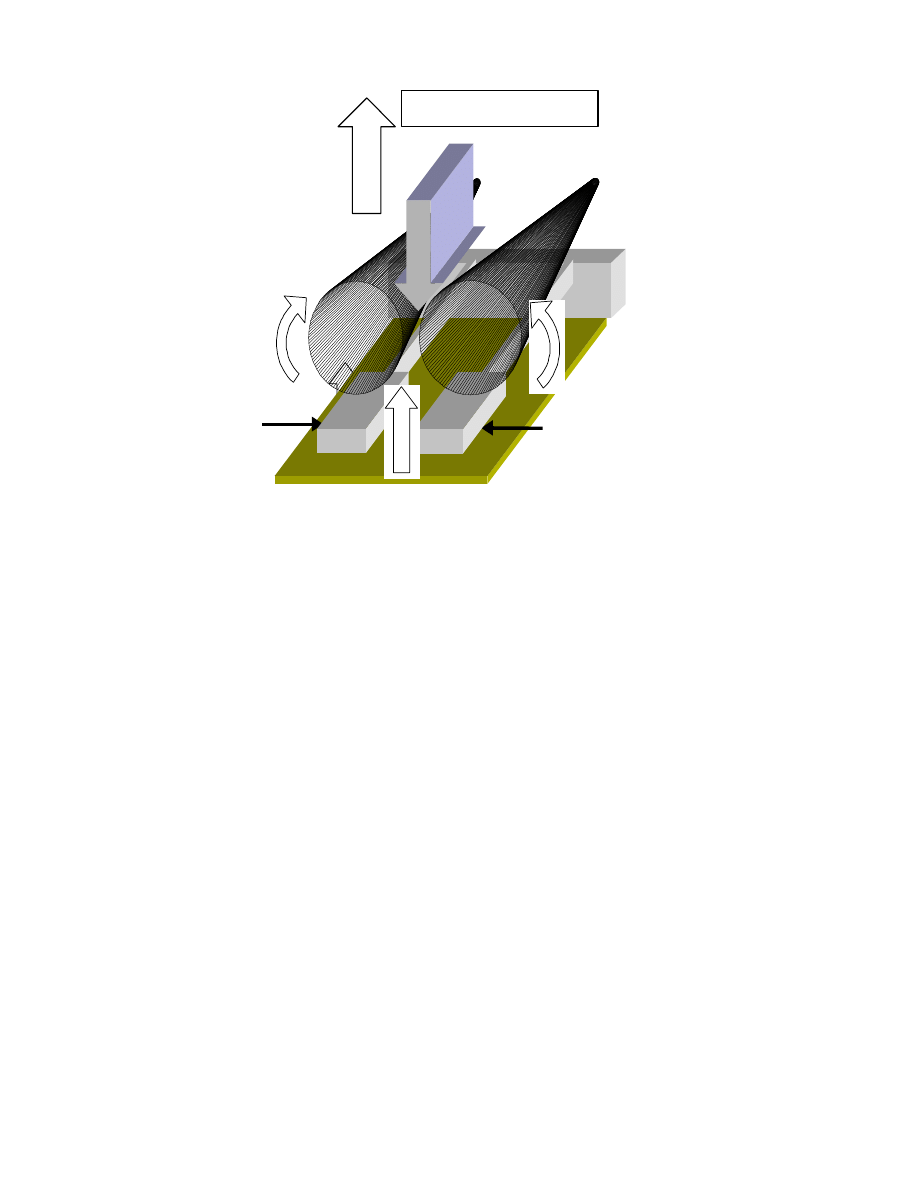
Flow Direction
Vortex
pair
Induced
flow
Actuator
motion
high speed
Vortex
pair
Actuator
motion
Induced
flow
Fig. 1
F. Sherman, S. Tung, C-J. Kim, C-M Ho, and J. Woo
16
Fig. 2
F. Sherman, S. Tung, C-J. Kim, C-M Ho, and J. Woo
17
0
5
10
15
20
25
30
35
0
20
40
60
80
100
120
140
160
180
Voltage (V)
Tip Deflection (um)
2 um width
with Ground
Effect
included
In-plane
actuator
Current
experimental
value
Legtenberg's
experimental [7]
Ansys results
with 1.6 um width
and ground
effect included
Fig. 3

F. Sherman, S. Tung, C-J. Kim, C-M Ho, and J. Woo
18
(a)
(b)
f=34.7 kHz
(c)
Fig. 4
F. Sherman, S. Tung, C-J. Kim, C-M Ho, and J. Woo
19
Silicon
(10-15
µ
m)
Oxide
(3
µ
m)
Deep RIE
(10-15
µ
m)
Timed etch
release
(a)
(b)
(c)
Fig. 5
F. Sherman, S. Tung, C-J. Kim, C-M Ho, and J. Woo
20
(a)
(b)
Fig. 6
F. Sherman, S. Tung, C-J. Kim, C-M Ho, and J. Woo
21
Flow
Actuator
Induced flow
Hot-wire
Fig. 7

F. Sherman, S. Tung, C-J. Kim, C-M Ho, and J. Woo
22
Fig. 8
Average Value
+ 0.1 Volt
- 0.1 Volt
Hot-wire output (volts)
0
2
4
6
8
Time (sec) (10
-3
)
Actuator off
Actuator on
F. Sherman, S. Tung, C-J. Kim, C-M Ho, and J. Woo
23
CCD camera
Laser sheet
Laser
source
Induced Flow
Fig. 9
Actuation
F. Sherman, S. Tung, C-J. Kim, C-M Ho, and J. Woo
24
Probe tip
Smoke delivery
system
1 cm X 1 cm
chip
Separation
Reflection
Stagnant
smoke
Up-lifted
smoke
Real
image
Reflective
image
Fig. 10
(b)
(c)
Wyszukiwarka
Podobne podstrony:
więcej podobnych podstron