PROJECTS
MICROCONTROLLERS
22
elektor - 12/2008
Bits on Parade
An I
2
C bus tester
Udo Jürsz and Wolfgang Rudolph (Germany)
This project puts the Elektor ATM18 AVR board to use as a tester for the Inter-Integrated Circuit bus. This
two-wire bus goes by various names, including IIC, I
2
C, and (at Atmel) TWI (for ‘two-wire interface’).
As this bus is very widely used, many microcontrollers have a built-in interface for it. The tool described
here can be used to perform quick, simple tests on I
2
C ICs and modules.
When engineers at Philips developed
the I
2
C bus 20 years ago, they prob-
ably didn’t have any idea how wide-
spread and important it would become.
Nowadays it forms an essential part
of many types of diagnostic and con-
trol systems and other products. It is
also used in most embedded applica-
tions. The reasons for this success are
readily apparent: with a data transmis-
sion rate of up to 3.4 Mbit/s and low
cost, it is an attractive option. It was
designed right from the start to enable
networking of multiple components. As
a bidirectional bus with a master/slave
architecture, the I
2
C bus does a very
good job of fulfilling this task.
Although its sof tware addressing
scheme and integrated protocol may
make it appear complex and cumber-
some at first, it is easy to use in prac-
tice. Its two signal lines, consisting of
a serial clock line (SCL) and a serial
data line (SDA), can be used to control
a large number of sensors or implement
communication tasks between micro-
controllers. The original data transfer
rate was 100 kbit/s, but in 1992 it was
increased by a factor of 4, and 1998 it
was boosted to a healthy 3.4 Mbit/s.
Its ‘clock stretching’ capability also
allows the bus to be used to service
very slow bus devices. With the lat-
est developments, it is now possible
to control well over 30 devices on each
bus segment.
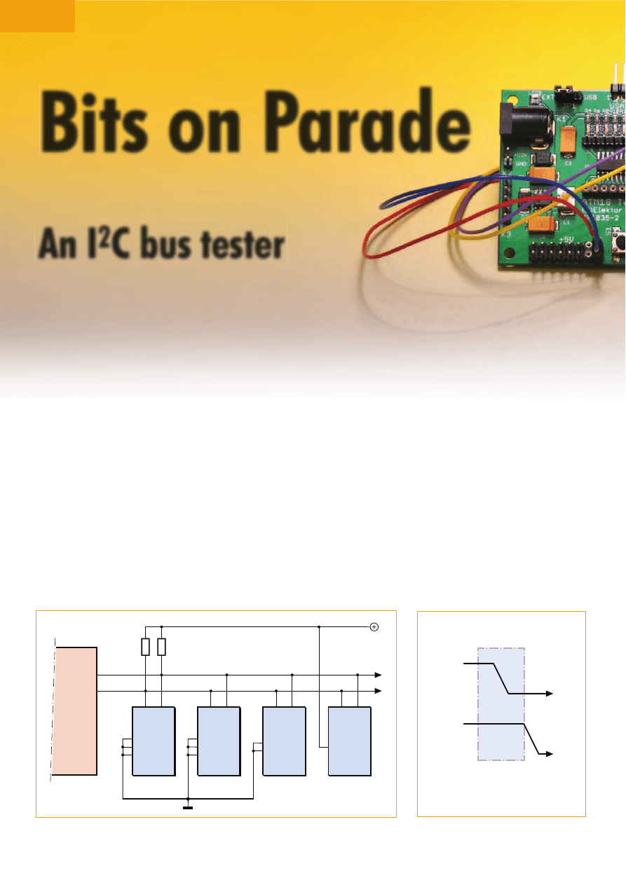
PCF8574
addr. 64
SCL
S
D
A
A0
A1
A2
addr. 144
PCF8591
SCL
S
D
A
A0
A1
A2
addr. 162
PCF8583
SCL
S
D
A
A0
addr. 160
24C512
SCL
S
D
A
A0
A1
2
k
2
2
k
2
Mega88
SDA
SCL
V
CC
PC5
PC4
080317 - 11
Figure 1. I
2
C bus with four slaves.
SDA
SCL
080317 - 12
start condition
Figure 2. Start condition: SDA goes low while SCL is high.
23
12/2008 - elektor
Protocol
Data is transmitted in both directions
on the bus. To enable access to indi-
vidual target devices, each I
2
C bus
IC has its own address. The I²C bus
protocol has a set of precisely defined
situations that allow each bus device
(slave) to recognise the start and end
of a transmission and whether it is
being addressed by the master device
(microcontroller). Both lines (SDA and
SCL) are high in the quiescent state
and thus inactive.
Start condition
The start condition indicates to the
devices on the bus that a data trans-
mission will follow. The start condition
is generated by changing the state of
the SDA line from high to low while
SCL is high (
Figure 1).
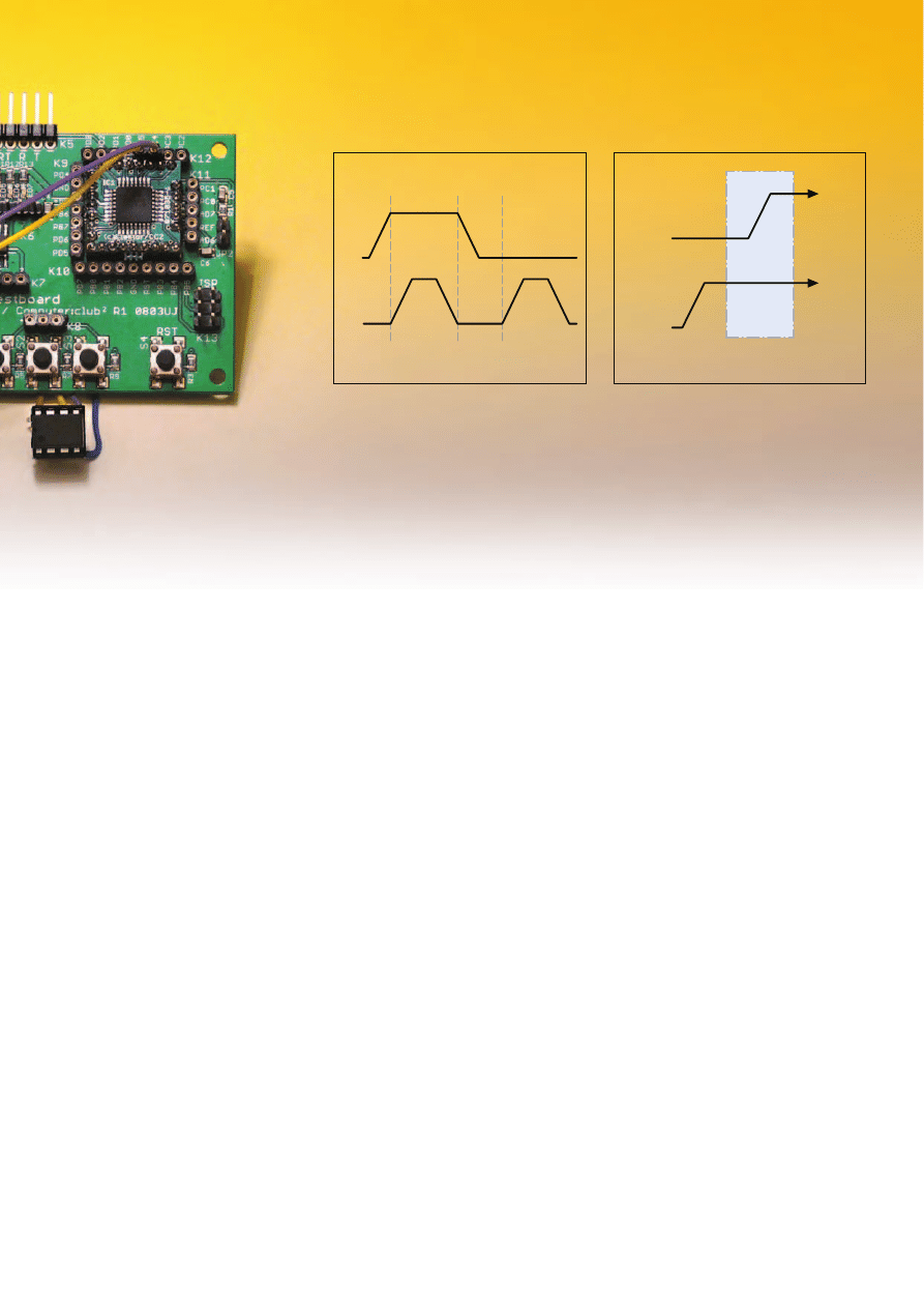
Data transmission
The currently active transmitter places
eight data bits on the data line (SDA),
which are shifted serially by the clock
signal pulses on the SCL line gener-
ated by the master (
Figure 3). The
data transfer starts with the most sig-
nificant bit.
Acknowledge
The currently active receiver acknowl-
edges the receipt of a byte pulling the
SDA line low while the master gen-
erates the ninth clock pulse on the
SCL line. This means that SDA goes
low during the ninth clock pulse on
the SCL line. The acknowledgement
also means that the receiver expects
to receive another byte. If the receiver
wishes to end the transmission, it must
indicate this by omitting the acknowl-
edgement. The actual end of the trans-
mission is achieved by generating the
stop condition.
Stop condition
The stop condition is the reverse of the
start condition with regard to the level
on the SDA line. In this case, SDA must
change from low to high while SCL is
high (
Figure 4). This ends the data
transmission.
Addresses are transmitted and
acknowledged in exactly the same
way as data. The following process
occurs in the simplest case, which is
a data transfer from the master to a
slave (such as a PCF8574 output port).
First, the master generates a start con-
dition and then transmits the address
of the port IC in bits 7–1, with the
desired data transmission direction
set in bit 0 (in this case ‘0’ for ‘write’).
The address is acknowledged by the
addressed slave device. The master
then sends a data byte, which is also
acknowledged. It can break the con-
nection now by generating a stop con-
dition, or it can send additional data
bytes to the same slave device.
This is all we want to say here about
the basic operation of the I
2
C bus.
There are many other interesting
things about the bus that could be
described, such as using several mas-
ters on a single bus, reserving the bus
(repeat start condition), byte trans-
fers and acknowledgement. Wikipe-
dia is a good source of further basic
information.
Addresses
In order to use the tester, you need
to know the device addresses. Every
type of IC has a base address. Some
examples are:
8574 port expander: 0x40 = 64 (decimal)
PCF8591 A/D converter: 0x90 = 144 (decimal)
EEPROMs: 0xA0 = 160 (decimal)
PCF8583 clock IC: 0xA0 = 160 (decimal)
The address byte contains eight
bits. With the usual 7-bit addressing
scheme, the remaining bit is used to
control the data transfer direction.
The master uses this bit to indicate
whether it wishes to send or receive
data, and it is called the ‘R/W bit’. For
example, ‘A1’ (decimal 161) can be
used to address an EEPROM for read-
ing. When an address is placed on the
bus, the addressed device acknowl-
edges receipt of the address, which
also indicates that it is ready to receive
or send data. If the master does not
receive an acknowledgement form the
addressed slave, the address was not
received correctly or the slave cannot
receive or send data.
Many types of ICs allow the last three
bits to be used as subaddresses. They
thus have three pins that can be con-
nected to GND (‘0’) or V
CC
(‘1’) as
appropriate. For example, you can con-
nect eight PCF8574 ICs to the same
bus and address them individually.
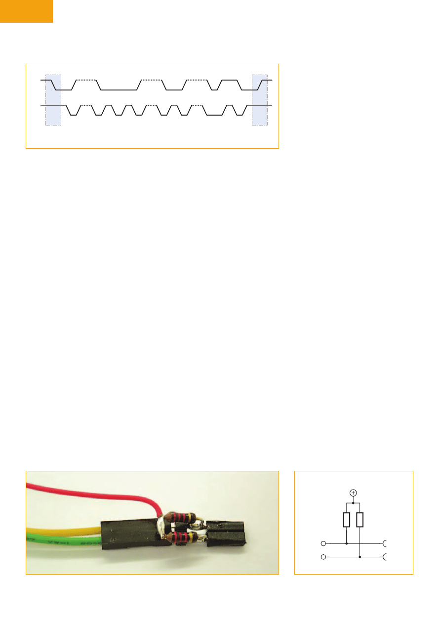
A full bus cycle is shown in schematic
form in
Figure 5. It begins with a start
SDA
SDA constant
SDA allowed to change
bit valid
SCL
080317 - 13
Figure 3. Each data bit is transferred when the signal on the
clock line (SCL) indicates that the data is valid.
SDA
SCL
080317 - 14
stop condition
Figure 4. Stop condition:
SDA goes high while SCL is high.
PROJECTS
MICROCONTROLLERS
24
elektor - 12/2008
condition, which is followed by the
address and R/W bit. After this, you
can see the acknowledgement, which
is followed by a byte transmitted by
the master. After this byte is acknowl-
edged, the master sends the next byte.
It is also acknowledged by the slave.
As the master does not have any more
data to send, it generates the stop
condition.
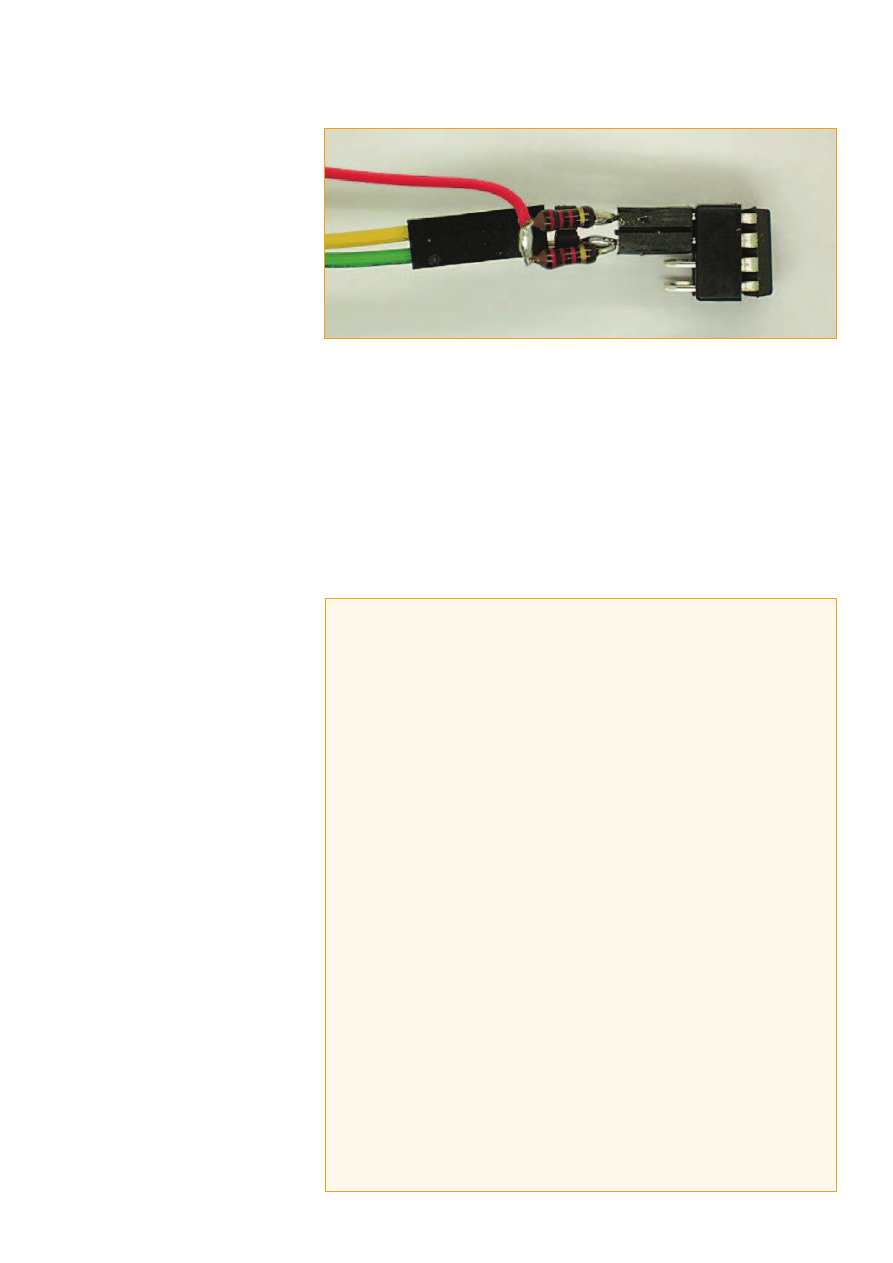
Minimal hardware
In order to use the I
2
C bus, you have
to put together a pull-up adapter (
Fig-
ure 6). A 2.2-k
7 resistor must be con-
nected to each of the two bus lines
(serial clock (SCL) on PC5 and serial
data (SDA) on PC4) to pull them up to
+5 V (
Figure 7).
If you want to connect more than one
device to the bus, the bus port must
have more than one socket or one set
of pins.
Figure 8 shows a serial EEP-
ROM with a capacity of 4 Kbits (such
as an ST24C04MN) connected to the
bus. Here the test adapter is connected
directly to the IC socket. In other situ-
ations, you could connect the tester to
one or more ICs on a prototyping strip-
board or a printed circuit board.
Tester software
STA = Set start condition
STP = Set stop condition
DRB = Direct read byte
DWB = Direct write byte
In theory, you can control any I
2
C IC
with these commands. For example,
suppose you want to send a byte to a
PCF8574 port expander to define the
states of its eight outputs.
Here you must remember that all data
is output in hexadecimal form, so the
address is ‘40’ (short for ‘0x40’) rather
than ‘64’. The data byte is ‘55’ (deci-
mal 85 or binary 01010101), which
means that after the transfer is com-
pleted alternating port pins are high
and low, which you can easily check
with a meter or logic tester.
Command:
Response:
STA // Start condition
0 // Executed
DWB 40 // Slave address
0 // Executed
DWB 55 // Data byte
0 // Executed
STP // Stop condition
0 // Executed
Now you can also read data from the
IC. Naturally, you expect the output
states you read back be the same as
what you sent. Here the address is
‘0x41’ because the R/W bit must be set
to 1. And indeed, you see that the read
byte is ‘0x55’.
Command:
Response:
STA // Start condition
0 // Executed
DWB 41 // Slave address
0 // Executed
DRB 0 // Read without ack
55 // Port data
STP // Stop condition
0 // Executed
For another example of using low-level
commands, you can write a byte to a
24C04 EEPROM with address ‘0x00’ as
follows:
A program that you can use for initial
testing is available for download from
the Elektor website or the Computer:
club² website. It supports several sim-
ple commands that can be used for
communication with the I
2
C bus inter-
face via the serial port of a PC. Load
the program
ATM18_I2C_Tester in the
microcontroller and connect the system
under test to a terminal emulator pro-
gram using communication port set-
tings 38400, N, 8, 1.
The following star t message will
appear after a reset:
ATM18 I2C_Tester V1.2
If you press the question mark key
(?) in response, a list of the available
commands will be displayed. There
are two types of commands: low-level
commands and high-level commands,
which are specifically designed for
controlling EEPROMs. The command
interpreter acknowledges each issued
command with a number in the range
of 0–3:
0 = Command executed
1 = Unknown command
2 = Incorrect or missing parameter(s)
3 = Error during command execution
The most important
low-level com-
mands are:
SDA
SCL
1- 7
address
acknowledgement
acknowledgement
(no)
acknowledgement
R/W
data
(1 Byte)
data
(1 Byte)
8
9
1- 8
9
1- 8
9
080317 - 15
start condition
stop condition
Figure 5. Data transfer with addressing and acknowledgement.
Figure 6. Test adapter construction.
2k2
2k2
V
CC
PC5
SCL
PC4
SDA
080317 - 16
Figure 7. Schematic diagram of the adapter.
25
12/2008 - elektor
Command:
Response:
STA // Start condition
0 // Executed
DWB A0 // Slave address
0 // Executed
DWB 00 // Byte address
0 // Executed
DWB 11 // Data byte
0 // Executed
STP // Stop condition
0 // Executed
To read data from the EEPROM, you
must first send the internal address of
the desired data with the R/W bit set
to ‘write’. After this, you must send
the address again with the R/W bit set
to ‘read’ in order to read one or more
bytes. The following example with
low-level commands demonstrates
reading one byte from address ‘0x00’:
Command:
Response:
STA // Start condition
0 // Executed
DWB A0 // Slave address
0 // Executed
DWB 00 // Byte address
0 // Executed
STA // Restart
0 // Executed
DWB A1 // Slave address
0 // Executed
DRB 0 // Read without ack
11 // EEPROM
data
STP // Stop condition
0 // Executed
High-level commands
With the high-level commands, you
only have to specify the slave address
and the byte address in order to read
or write an EEPROM directly. The
interpreter handles the addressing
and generates the start and stop con-
ditions all on its own. Here again, all
data is communicated in hexadecimal
form.
RSB = Read single byte
RDB = Read double byte
RMB = Read multiple bytes
WSB = Write single byte
WDB = Write double byte
WMB = Write multiple bytes
‘Set’ commands:
SA = Set slave Address
BA = Set byte address
‘Get’ commands:
SA? = Get slave address
BA? = Get byte address
IDN? = Get identity string
? = Get help
High-level examples
Writing several bytes to a 24C04 EEP-
ROM starting at address ‘0x00’:
Command:
Response:
SA A0 // Slave address
0 // Executed
BA 00 // Byte address
0 // Executed
WMB 11 22 33 44 55 // 5 bytes
0 // Executed
Reading several bytes from a 24C04
EEPROM starting at address ‘0x00’:
Command:
Response:
SA A0 // Slave address
0 // Command
execution acknowledgement
BA 00 // Byte address
0 // Command
execution acknowledgement
RMB 5 // Read 5 bytes
11,22,33,44,55// EEPROM data
Figure 8. Testing a 14V04 EEPROM.
Reserved addresses and 10-bit addressing
Certain I
2
C addresses are reserved and cannot be used for connected devices. Due to these
reserved addresses, only 112 of the 128 addresses possible with 7-bit addressing are avail-
able for use.
Address
R/W bit
Description
0000000
0
General call address
0000001
x
CBUS address
0000010
x
Reserved for a different bus format
0000011
x
Reserved for future expansion
00001xx
x
Reserved for future expansion
11111xx
x
Reserved for future expansion
11110xx
x
R8C/13 applications
In order to handle a growing number of new I
2
C ICs, 10-bit addresses were introduced. This
makes it possible to address up to 1024 devices on a single bus. Thanks to the use of previ-
ously unused addresses in the ‘1111 ‘0xx’ range together with the R/W bit, there is no interfer-
ence to 7-bit devices on the same bus, so 7-bit and 10-bit devices can be used together on
the same bus.
10-bit marker
Address part 1
R/W bit
Address part 2
11110
XX
X
Acknowledge 1
XXXXXXXX
Acknowledge 2
The five bits of the reserved address ‘11110’ are sent first, followed by the first two bits of the
device address. The R/W bit is sent next, since an acknowledgement follows every byte. Of
course, more than one device may respond to the first part of the address, and they can all
send an acknowledgement. The second part of the address is sent after the acknowledgement.
All bus devices selected by the first part of the address also decode the second address byte. In
a properly configured network, there can be only one device that generates an acknowledge-
ment after this. Now the communication can begin.

PROJECTS
MICROCONTROLLERS
26
elektor - 12/2008
Finding addresses with Bascom
In a situation where several ICs with
jumper-programmable subaddresses
are present on a bus or you want to
investigate an unknown system,
you often do not know the I
2
C slave
addresses. A small program written
with Bascom can help here. It tries
each address in turn to see whether a
device responds. Each time an address
is sent, the system variable ERR is
assigned a ‘1’ if no acknowledgement
is received or to ‘0’ if an acknowledge-
ment is received, which means that the
address is valid. The program tests all
even-numbered addresses in the range
of 0 to 254, since the corresponding
odd-numbered addresses would be the
read address of the same ICs.
This program (see
Listing 1) generates
a list of addresses in decimal notation,
such as the following example:
ATM18 I2C address test
64
144
160
162
Here the ICs show in
Figure 1 were
found. Although the PCF8583 clock IC
has the same base address as every
EEPROM, in order to avoid an address
conflict its subaddress is altered by
connecting its A0 pin to V
CC
so that
a basic tool for software control of all
types of devices and machinery. The
program (see
Listing 3) also transmits
the data via the serial interface for
auditing or checking.
Reading the individual bytes from the
EEPROM requires the same actions
as for low-level control of the 24C04,
except that here the byte address is
transmitted in two parts (high byte and
low byte). After this, the I
2
C address
must be sent again with the R/W bit
set to ‘read’(address ‘161’ instead of
‘160’) in order to read the data. ACK is
used in I2CRBYTE for the actual read-
ing process, and if more than one byte
must be transferred, the final byte is
fetched with NACK.
(080317-I)
it appears at address ‘162’ instead of
address ‘160’.
Writing data to an EEPROM
Here we use a 24C512 EEPROM, which
has a total capacity of 64 KB. This rel-
atively large address space requires
using a 16-bit address for the stored
data. Consequently, two internal
address bytes are sent after the I
2
C
addressing cycle. They are followed
by one or more data bytes. The pro-
gram (see
Listing 2) receives individ-
ual bytes from the serial interface and
stores them in the EEPROM starting at
address ‘0’.
Data output to a port expander
The objective here is to read data
from an EEPROM and transfer it to a
PDF9574 port expander. This gives you
Listing 1
Finding addresses with Bascom
‘ATM18 I2C tester
‘I2C: SCL = PC5, SDA = PC4
$regfile = “m88def.dat”
$crystal = 16000000
Baud = 38400
Dim N As Byte
Config Portb = Output
Config Scl = Portc.5
Config Sda = Portc.4
Print “ATM18 I2C ad-
dress test”
For N = 2 To 254 Step 2
I2cstart
I2cwbyte N
If Err = 0 Then Print N
I2cwbyte 0x55
I2cstop
Next N
End
The ATM18 project at Computer:club
2
ATM18 is a joint project of Elektor and Computer:club2 (www.cczwei.de) in collaboration with
Udo Jürß, the editor in chief of www.microdrones.de. The latest developments and applica-
tions of the ATM18 are presented by Computer:club
2
member Wolfgang Rudolph in the CC2-
tv programme broadcast on the German NRW-TV channel. The ATM18-AVR board with the
I
2
C tester was featured in instalment 24 of CC
2
-tv, which was first broadcast on 23 October
2008.
CC2-tv is broadcast live by NRW-TV via the cable television network in North Rhine–West-
phalia and as a LiveStream programme via the Internet (www.nrw.tv/home/cc2). CC2-tv is
also available as a podcast from www.cczwei.de and – a few days later – from sevenload.de.
Listing 2
Writing data to an EEPROM
$regfile = “m88def.dat”
$crystal = 16000000
Baud = 38400
Dim N As Byte
Dim Adr As Word
Dim H As Byte
Dim L As Byte
Dim Dat As Byte
Config Portb = Output
Config Scl = Portc.5
Config Sda = Portc.4
Print “ATM18 24C512 write”
For Adr = 0 To 1000
Input Dat ‘start
I2cstart
I2cwbyte 160 ‘slave adsress 24C512
H = High(adr)
L = Low(adr)
I2cwbyte H ‘high address
I2cwbyte L ‘low address
I2cwbyte Dat ‘write byte
I2cstop ‘stop
Next Adr
End
Wyszukiwarka
Podobne podstrony:
I2C bus specificaion 2000 id 20 Nieznany
I2C Bus Implementierung
I2C BUS SPECIFICATION 2
Automotive On Board Diagnostics II Bus, ODBII Description
I2C BUS SPECIFICATION 3
Rage Against the Machine Bulls on Parade
NXP i2c bus specification
Don t turn your back on science An open letter
Galvanische Trennung fuer I2C Bus
Interruption of the blood supply of femoral head an experimental study on the pathogenesis of Legg C
Pancharatnam A Study on the Computer Aided Acoustic Analysis of an Auditorium (CATT)
An Essay on Mozambique
AVT 5321 Szukacz i tester układów na magistrali I2C
comment on 'Quantum creation of an open universe' by Andrei Linde
więcej podobnych podstron