LM137/LM337
3-Terminal Adjustable Negative Regulators
General Description
The LM137/LM337 are adjustable 3-terminal negative volt-
age regulators capable of supplying in excess of −1.5A over
an output voltage range of −1.2V to −37V. These regulators
are exceptionally easy to apply, requiring only 2 external
resistors to set the output voltage and 1 output capacitor for
frequency compensation. The circuit design has been opti-
mized for excellent regulation and low thermal transients.
Further, the LM137 series features internal current limiting,
thermal shutdown and safe-area compensation, making
them virtually blowout-proof against overloads.
The LM137/LM337 serve a wide variety of applications in-
cluding local on-card regulation, programmable-output volt-
age regulation or precision current regulation. The LM137/
LM337 are ideal complements to the LM117/LM317
adjustable positive regulators.
Features
n
Output voltage adjustable from −1.2V to −37V
n
1.5A output current guaranteed, −55˚C to +150˚C
n
Line regulation typically 0.01%/V
n
Load regulation typically 0.3%
n
Excellent thermal regulation, 0.002%/W
n
77 dB ripple rejection
n
Excellent rejection of thermal transients
n
50 ppm/˚C temperature coefficient
n
Temperature-independent current limit
n
Internal thermal overload protection
n
P
+
Product Enhancement tested
n
Standard 3-lead transistor package
n
Output is short circuit protected
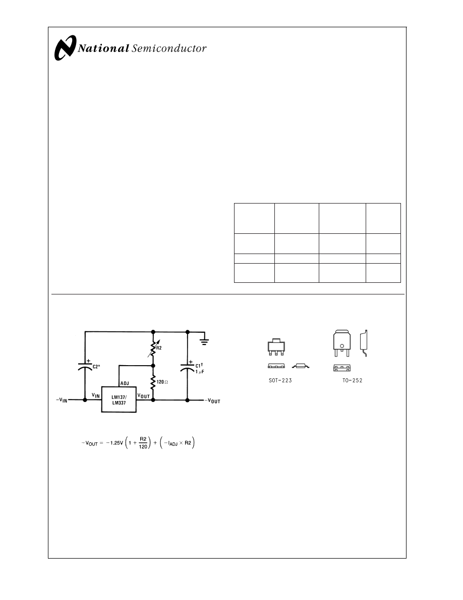
LM137 Series Packages and Power Capability
Rated
Design
Device
Package
Power
Load
Dissipation
Current
LM137/337
TO-3 (K)
20W
1.5A
TO-39 (H)
2W
0.5A
LM337
TO-220 (T)
15W
1.5A
LM337
SOT-223
(MP)
2W
1A
Typical Applications
Adjustable Negative Voltage Regulator
00906701
Full output current not available at high input-output voltages
†
C1 = 1 µF solid tantalum or 10 µF aluminum electrolytic required for
stability
*C2 = 1 µF solid tantalum is required only if regulator is more than 4" from
power-supply filter capacitor
Output capacitors in the range of 1 µF to 1000 µF of aluminum or tantalum
electrolytic are commonly used to provide improved output impedance and
rejection of transients
Comparison between SOT-223 and
D-Pak (TO-252) Packages
00906731
Scale 1:1
November 2001
LM137/LM337
3-T
erminal
Adjustable
Negative
Regulators
© 2001 National Semiconductor Corporation
DS009067
www.national.com
Absolute Maximum Ratings
(Notes 1,
If Military/Aerospace specified devices are required,
please contact the National Semiconductor Sales Office/
Distributors for availability and specifications.
Power Dissipation
Internally Limited
Input-Output Voltage Differential
40V
Operating Junction Temperature
Range
LM137
−55˚C to +150˚C
LM337
0˚C to +125˚C
LM337I
−40˚C to +125˚C
Storage Temperature
−65˚C to +150˚C
Lead Temperature (Soldering, 10 sec.)
300˚C
Plastic Package (Soldering, 4 sec.)
260˚C
ESD Rating
2k Volts
Electrical Characteristics
Parameter
Conditions
LM137
LM337
Units
Min
Typ
Max
Min
Typ
Max
Line Regulation
T
j
= 25˚C, 3V
≤
|V
IN
− V
OUT
|
≤
40V
0.01
0.02
0.01
0.04
%/V
(Note 2) I
L
= 10 mA
Load Regulation
T
j
= 25˚C, 10 mA
≤
I
OUT
≤
I
MAX
0.3
0.5
0.3
1.0
%
Thermal Regulation
T
j
= 25˚C, 10 ms Pulse
0.002
0.02
0.003
0.04
%/W
Adjustment Pin Current
65
100
65
100
µA
Adjustment Pin Current Charge
10 mA
≤
I
L
≤
I
MAX
2
5
2
5
µA
3.0V
≤
|V
IN
− V
OUT
|
≤
40V,
T
A
= 25˚C
Reference Voltage
T
j
= 25˚C (Note 3)
−1.225 −1.250 −1.275 −1.213 −1.250 −1.287
V
3V
≤
|V
IN
− V
OUT
|
≤
40V, (Note 3)
−1.200 −1.250 −1.300 −1.200 −1.250 −1.300
V
10 mA
≤
I
OUT
≤
I
MAX
, P
≤
P
MAX
Line Regulation
3V
≤
|V
IN
− V
OUT
|
≤
40V, (Note 2)
0.02
0.05
0.02
0.07
%/V
Load Regulation
10 mA
≤
I
OUT
≤
I
MAX
, (Note 2)
0.3
1
0.3
1.5
%
Temperature Stability
T
MIN
≤
T
j
≤
T
MAX
0.6
0.6
%
Minimum Load Current
|V
IN
− V
OUT
|
≤
40V
2.5
5
2.5
10
mA
|V
IN
− V
OUT
|
≤
10V
1.2
3
1.5
6
mA
Current Limit
|V
IN
− V
OUT
|
≤
15V
K, MP and T Package
1.5
2.2
3.5
1.5
2.2
3.7
A
H Package
0.5
0.8
1.8
0.5
0.8
1.9
A
|V
IN
− V
OUT
| = 40V, T
j
= 25˚C
K, MP and T Package
0.24
0.4
0.15
0.4
A
H Package
0.15
0.17
0.10
0.17
A
RMS Output Noise, % of V
OUT
T
j
= 25˚C, 10 Hz
≤
f
≤
10 kHz
0.003
0.003
%
Ripple Rejection Ratio
V
OUT
= −10V, f = 120 Hz
60
60
dB
C
ADJ
= 10 µF
66
77
66
77
dB
Long-Term Stability
T
j
= 125˚C, 1000 Hours
0.3
1
0.3
1
%
Thermal Resistance, Junction to
Case
H Package
12
15
12
15
˚C/W
K Package
2.3
3
2.3
3
˚C/W
T Package
4
˚C/W
Thermal Resistance, Junction to
Ambient (No Heat Sink)
H Package
140
140
˚C/W
K Package
35
35
˚C/W
T Package
MP Package
50
170
˚C/W
˚C/W
Note 1: Unless otherwise specified, these specifications apply −55˚C
≤
T
j
≤
+150˚C for the LM137, 0˚C
≤
T
j
≤
+125˚C for the LM337; V
IN
− V
OUT
= 5V; and I
OUT
= 0.1A for the TO-39 package and I
OUT
= 0.5A for the TO-3, SOT-223 and TO-220 packages. Although power dissipation is internally limited, these specifications
are applicable for power dissipations of 2W for the TO-39 and SOT-223 (see Application Hints), and 20W for the TO-3, and TO-220. I
MAX
is 1.5A for the TO-3,
SOT-223 and TO-220 packages, and 0.2A for the TO-39 package.
Note 2: Regulation is measured at constant junction temperature, using pulse testing with a low duty cycle. Changes in output voltage due to heating effects are
covered under the specification for thermal regulation. Load regulation is measured on the output pin at a point
1
⁄
8
" below the base of the TO-3 and TO-39 packages.
LM137/LM337
www.national.com
2
Electrical Characteristics
(Note 1) (Continued)
Note 3: Selected devices with tightened tolerance reference voltage available.
Note 4: Refer to RETS137H drawing for LM137H or RETS137K drawing for LM137K military specifications.
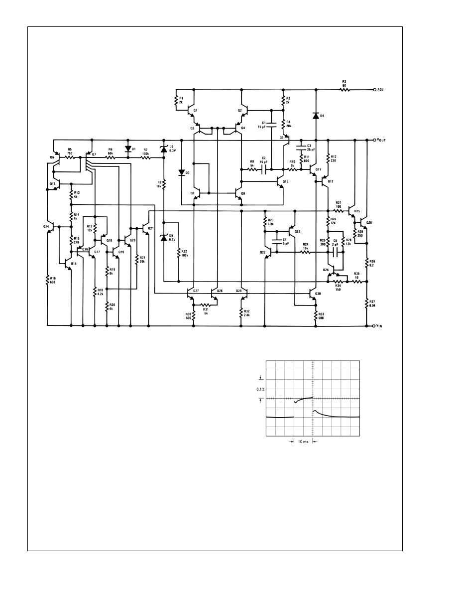
Schematic Diagram
00906702
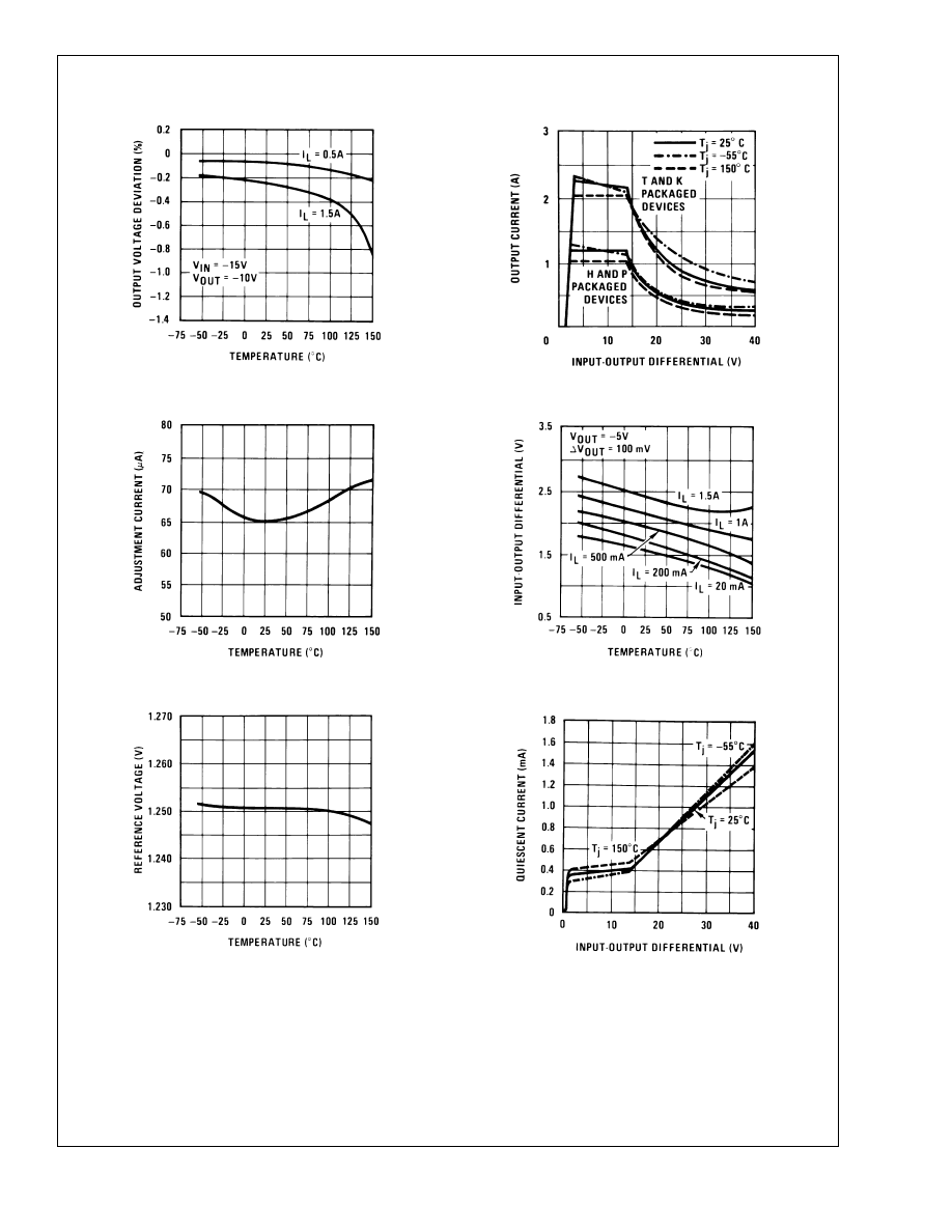
Thermal Regulation
When power is dissipated in an IC, a temperature gradient
occurs across the IC chip affecting the individual IC circuit
components. With an IC regulator, this gradient can be es-
pecially severe since power dissipation is large. Thermal
regulation is the effect of these temperature gradients on
output voltage (in percentage output change) per Watt of
power change in a specified time. Thermal regulation error is
independent of electrical regulation or temperature coeffi-
cient, and occurs within 5 ms to 50 ms after a change in
power dissipation. Thermal regulation depends on IC layout
as well as electrical design. The thermal regulation of a
voltage regulator is defined as the percentage change of
V
OUT
, per Watt, within the first 10 ms after a step of power is
applied. The LM137’s specification is 0.02%/W, max.
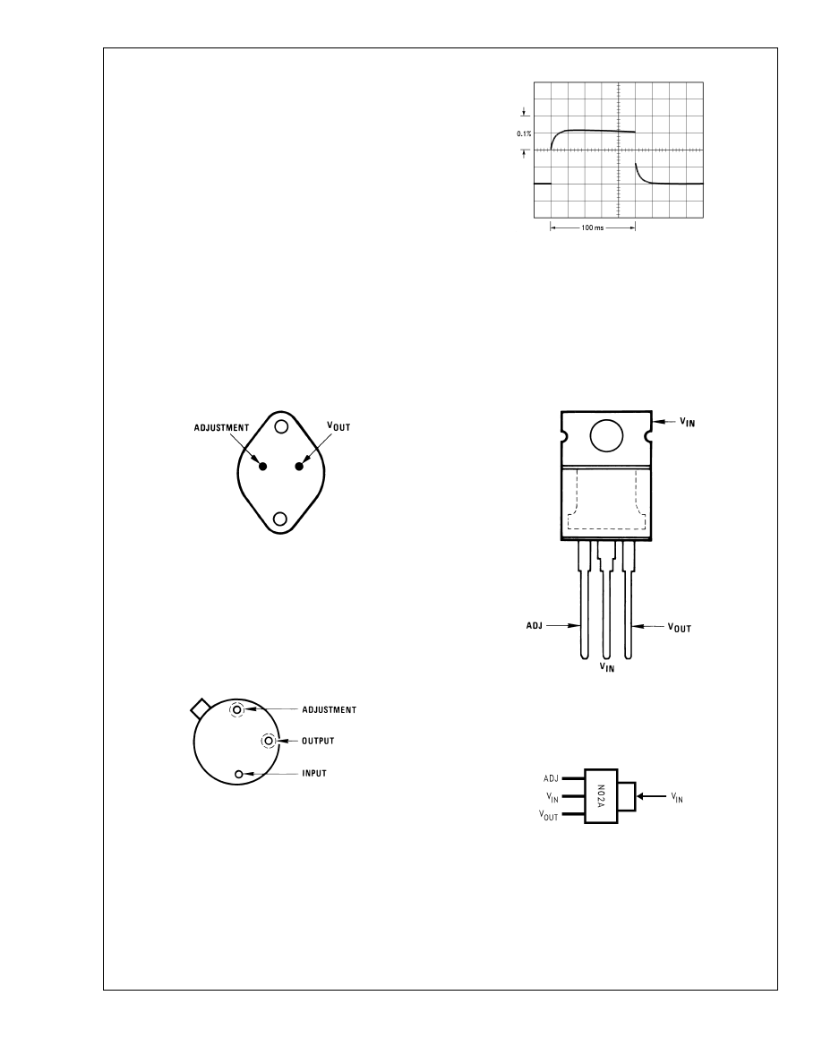
00906703
LM137, V
OUT
= −10V
V
IN
− V
OUT
= −40V
I
IL
= 0A
→
0.25A
→
0A
Vertical sensitivity, 5 mV/div
FIGURE 1.
LM137/LM337
www.national.com
3
Thermal Regulation
(Continued)
In
Figure 1, a typical LM137’s output drifts only 3 mV (or
0.03% of V
OUT
= −10V) when a 10W pulse is applied for
10 ms. This performance is thus well inside the specification
limit of 0.02%/W x 10W = 0.2% max. When the 10W pulse is
ended, the thermal regulation again shows a 3 mV step at
the LM137 chip cools off. Note that the load regulation error
of about 8 mV (0.08%) is additional to the thermal regulation
error. In
Figure 2, when the 10W pulse is applied for 100 ms,
the output drifts only slightly beyond the drift in the first
10 ms, and the thermal error stays well within 0.1% (10 mV).
Connection Diagrams
TO-3
Metal Can Package
00906705
Bottom View
Order Number LM137K/883
LM137KPQML and LM137KPQMLV(Note 5)
See NS Package Number K02C
Order Number LM337K STEEL
See NS Package Number K02A
Case is Input
TO-39
Metal Can Package
00906706
Bottom View
Order Number LM137H, LM137H/883 or LM337H
LM137HPQML and LM137HPQMLV(Note 5)
See NS Package Number H03A
Case Is Input
Note 5: See STD Mil DWG 5962P99517 for Radiation Tolerant Devices
TO-220
Plastic Package
00906707
Front View
Order Number LM337T
See NS Package Number T03B
3-Lead SOT-223
00906734
Front View
Order Number LM337IMP
Package Marked N02ASee NS Package Number MA04A
00906704
LM137, V
OUT
= −10V
V
IN
− V
OUT
= −40V
I
L
= 0A
→
0.25A
→
0A
Horizontal sensitivity, 20 ms/div
FIGURE 2.
LM137/LM337
www.national.com
4
Application Hints
When a value for
θ
(H−A)
is found using the equation shown,
a heatsink must be selected that has a value that is less than
or equal to this number.
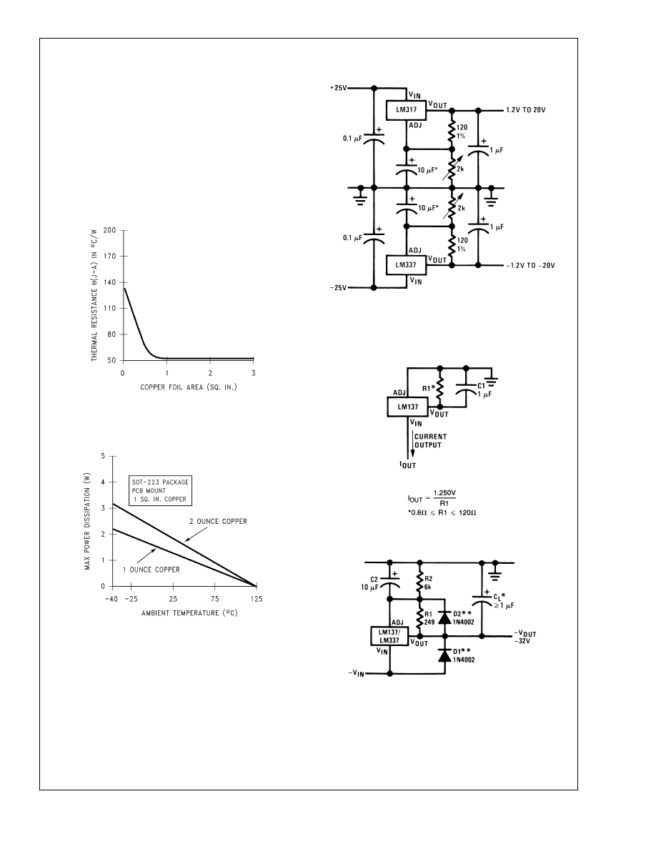
HEATSINKING SOT-223 PACKAGE PARTS
The SOT-223 (“MP”) packages use a copper plane on the
PCB and the PCB itself as a heatsink. To optimize the heat
sinking ability of the plane and PCB, solder the tab of the
package to the plane.
Figures 3, 4 show the information for the SOT-223 package.
Figure 4 assumes a
θ
(J−A)
of 75˚C/W for 1 ounce copper and
51˚C/W for 2 ounce copper and a maximum junction tem-
perature of 125˚C.
Please see AN1028 for power enhancement techniques to
be used with the SOT-223 package.
Typical Applications
Adjustable Lab Voltage Regulator
00906709
Full output current not available
at high input-output voltages
*The 10 µF capacitors are optional to improve ripple rejection
Current Regulator
00906711
Negative Regulator with Protection Diodes
00906713
*
When C
L
is larger than 20 µF, D1 protects the LM137 in case the input
supply is shorted
**
When C2 is larger than 10 µF and −V
OUT
is larger than −25V, D2
protects the LM137 in case the output is shorted
00906732
FIGURE 3.
θ
(J−A)
vs Copper (2 ounce) Area for the
SOT-223 Package
00906733
FIGURE 4. Maximum Power Dissipation vs. T
AMB
for
the SOT-223 Package
LM137/LM337
www.national.com
5
Typical Applications
(Continued)
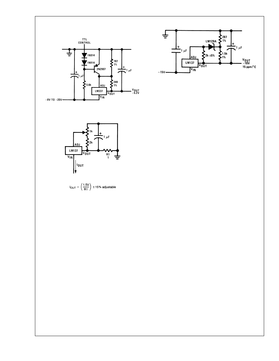
−5.2V Regulator with Electronic Shutdown
*
00906710
*Minimum output
.
−1.3V when control input is low
Adjustable Current Regulator
00906712
High Stability −10V Regulator
00906714
LM137/LM337
www.national.com
6
Typical Performance Characteristics
(K Steel and T Packages)
Load Regulation
Current Limit
00906716
00906717
Adjustment Current
Dropout Voltage
00906718
00906719
Temperature Stability
Minimum Operating Current
00906720
00906721
LM137/LM337
www.national.com
7
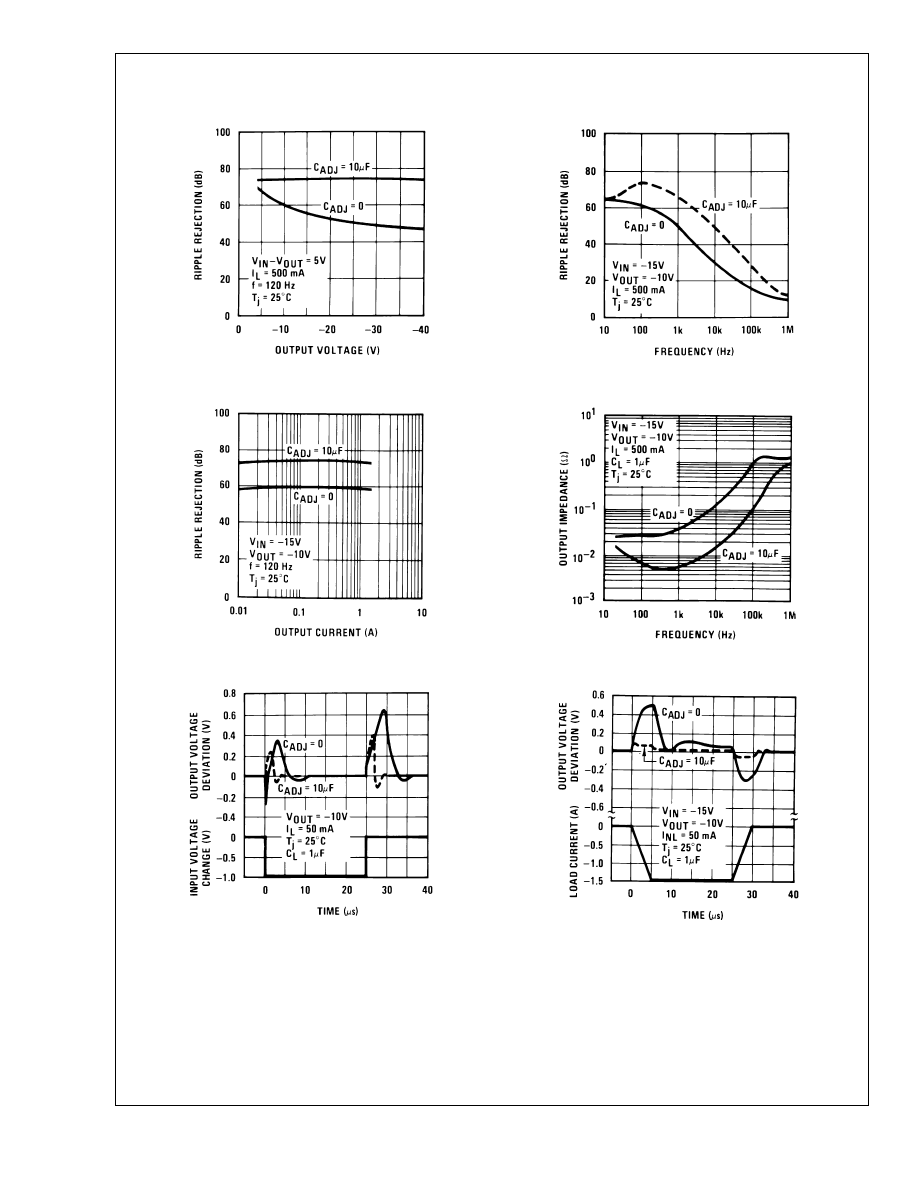
Typical Performance Characteristics
(K Steel and T Packages) (Continued)
Ripple Rejection
Ripple Rejection
00906722
00906723
Ripple Rejection
Output Impedance
00906724
00906725
Line Transient Response
Load Transient Response
00906726
00906727
LM137/LM337
www.national.com
8
Physical Dimensions
inches (millimeters)
unless otherwise noted
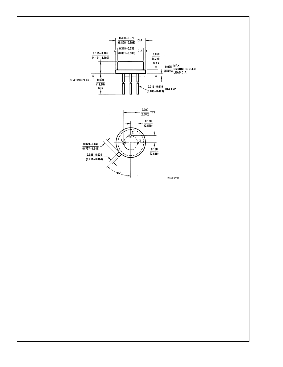
Metal Can Package (H)
Order Number LM137H, LM137H/883 or LM337H
NS Package Number H03A
LM137/LM337
www.national.com
9
Physical Dimensions
inches (millimeters) unless otherwise noted (Continued)
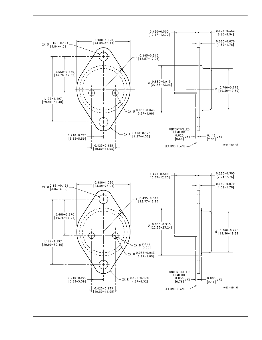
Metal Can Package (K)
Order Number LM337K STEEL
NS Package Number K02A
Mil-Aero Metal Can Package (K)
Order Number LM137K/883
NS Package Number K02C
LM137/LM337
www.national.com
10
Physical Dimensions
inches (millimeters) unless otherwise noted (Continued)
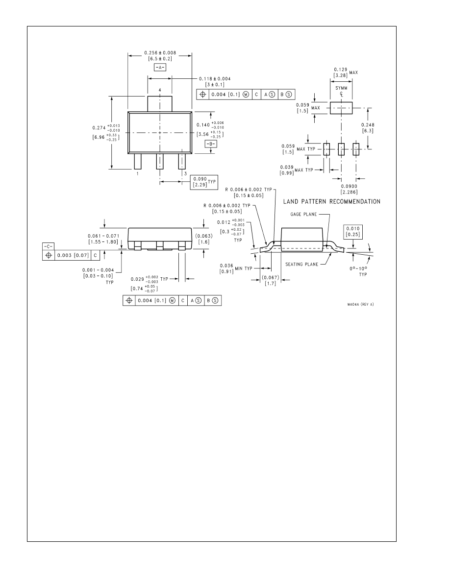
3-Lead SOT-223 Package
Order Number LM337IMP
NS Package Number M04A
LM137/LM337
www.national.com
11
Physical Dimensions
inches (millimeters) unless otherwise noted (Continued)
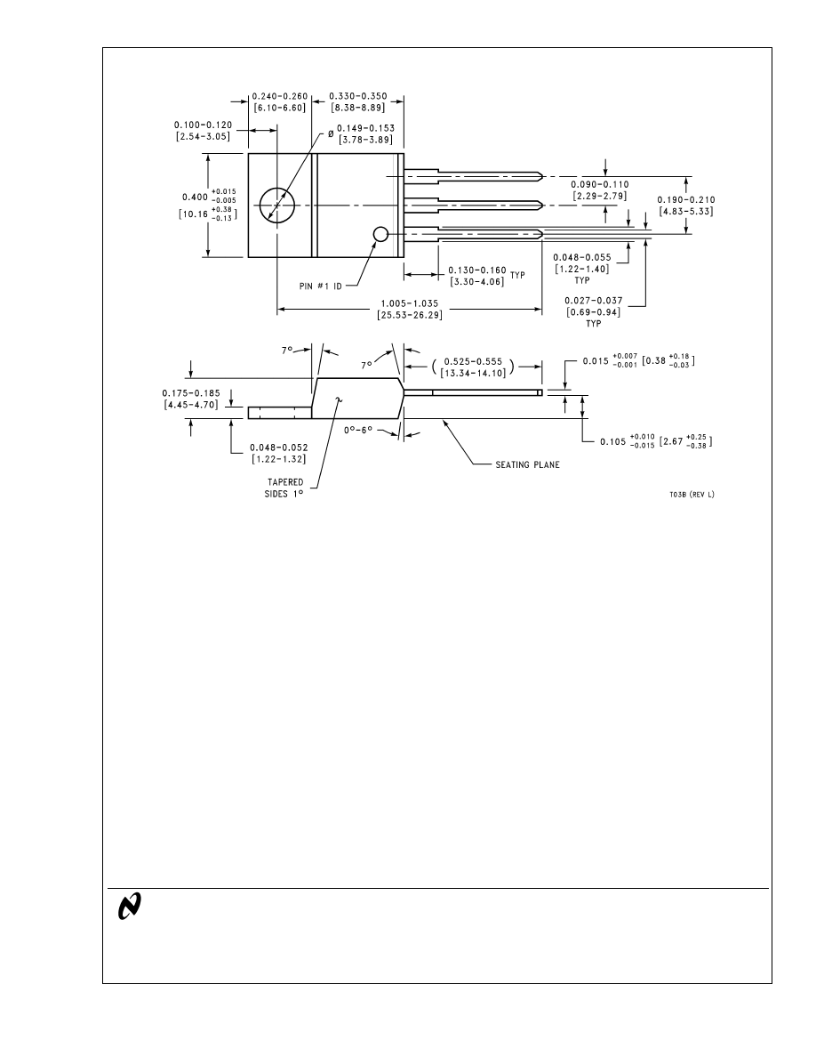
TO-220 Plastic Package (T)
Order Number LM337T
NS Package Number T03B
LIFE SUPPORT POLICY
NATIONAL’S PRODUCTS ARE NOT AUTHORIZED FOR USE AS CRITICAL COMPONENTS IN LIFE SUPPORT
DEVICES OR SYSTEMS WITHOUT THE EXPRESS WRITTEN APPROVAL OF THE PRESIDENT AND GENERAL
COUNSEL OF NATIONAL SEMICONDUCTOR CORPORATION. As used herein:
1. Life support devices or systems are devices or
systems which, (a) are intended for surgical implant
into the body, or (b) support or sustain life, and
whose failure to perform when properly used in
accordance with instructions for use provided in the
labeling, can be reasonably expected to result in a
significant injury to the user.
2. A critical component is any component of a life
support device or system whose failure to perform
can be reasonably expected to cause the failure of
the life support device or system, or to affect its
safety or effectiveness.
National Semiconductor
Corporation
Americas
Email: support@nsc.com
National Semiconductor
Europe
Fax: +49 (0) 180-530 85 86
Email: europe.support@nsc.com
Deutsch Tel: +49 (0) 69 9508 6208
English
Tel: +44 (0) 870 24 0 2171
Français Tel: +33 (0) 1 41 91 8790
National Semiconductor
Asia Pacific Customer
Response Group
Tel: 65-2544466
Fax: 65-2504466
Email: ap.support@nsc.com
National Semiconductor
Japan Ltd.
Tel: 81-3-5639-7560
Fax: 81-3-5639-7507
www.national.com
LM137/LM337
3-T
erminal
Adjustable
Negative
Regulators
National does not assume any responsibility for use of any circuitry described, no circuit patent licenses are implied and National reserves the right at any time without notice to change said circuitry and specifications.
Document Outline
- LM137/LM337
- General Description
- Features
- Typical Applications
- Comparison between SOT-223 and D-Pak (TO-252) Packages
- Absolute Maximum Ratings
- Electrical Characteristics (Note 1)
- Schematic Diagram
- Thermal Regulation
- Connection Diagrams
- Application Hints
- Typical Applications
- Typical Performance Characteristics
- Physical Dimensions
Wyszukiwarka
Podobne podstrony:
LM137 337
LM137
LM337
lm337
LM137,237,337
LM337N LM137
LM337
więcej podobnych podstron