
Chapter 2
Review of Circuit Theory
Literature Number SLOA074
Excerpted from
Op Amps for Everyone
Literature Number: SLOD006A

2-1
Review of Circuit Theory
Ron Mancini
2.1
Introduction
Although this book minimizes math, some algebra is germane to the understanding of
analog electronics. Math and physics are presented here in the manner in which they are
used later, so no practice exercises are given. For example, after the voltage divider rule
is explained, it is used several times in the development of other concepts, and this usage
constitutes practice.
Circuits are a mix of passive and active components. The components are arranged in
a manner that enables them to perform some desired function. The resulting arrangement
of components is called a circuit or sometimes a circuit configuration. The art portion of
analog design is developing the circuit configuration. There are many published circuit
configurations for almost any circuit task, thus all circuit designers need not be artists.
When the design has progressed to the point that a circuit exists, equations must be writ-
ten to predict and analyze circuit performance. Textbooks are filled with rigorous methods
for equation writing, and this review of circuit theory does not supplant those textbooks.
But, a few equations are used so often that they should be memorized, and these equa-
tions are considered here.
There are almost as many ways to analyze a circuit as there are electronic engineers, and
if the equations are written correctly, all methods yield the same answer. There are some
simple ways to analyze the circuit without completing unnecessary calculations, and
these methods are illustrated here.
2.2
Laws of Physics
Ohm’s law is stated as V=IR, and it is fundamental to all electronics. Ohm’s law can be
applied to a single component, to any group of components, or to a complete circuit. When
the current flowing through any portion of a circuit is known, the voltage dropped across
that portion of the circuit is obtained by multiplying the current times the resistance (Equa-
tion 2–1).
Chapter 2

Laws of Physics
2-2
(2–1)
V
+
IR
In Figure 2–1, Ohm’s law is applied to the total circuit. The current, (I) flows through the
total resistance (R), and the voltage (V) is dropped across R.
V
R
I
Figure 2–1. Ohm’s Law Applied to the Total Circuit
In Figure 2–2, Ohm’s law is applied to a single component. The current (I
R
) flows through
the resistor (R) and the voltage (V
R
) is dropped across R. Notice, the same formula is used
to calculate the voltage drop across R even though it is only a part of the circuit.
V
R
IR
VR
Figure 2–2. Ohm’s Law Applied to a Component
Kirchoff’s voltage law states that the sum of the voltage drops in a series circuit equals
the sum of the voltage sources. Otherwise, the source (or sources) voltage must be
dropped across the passive components. When taking sums keep in mind that the sum
is an algebraic quantity. Kirchoff’s voltage law is illustrated in Figure 2–3 and Equations
2–2 and 2–3.
V
R2
R1
VR1
VR2
Figure 2–3. Kirchoff’s Voltage Law
(2–2)
ȍ
V
SOURCES
+
ȍ
V
DROPS
(2–3)
V
+
V
R1
)
V
R2
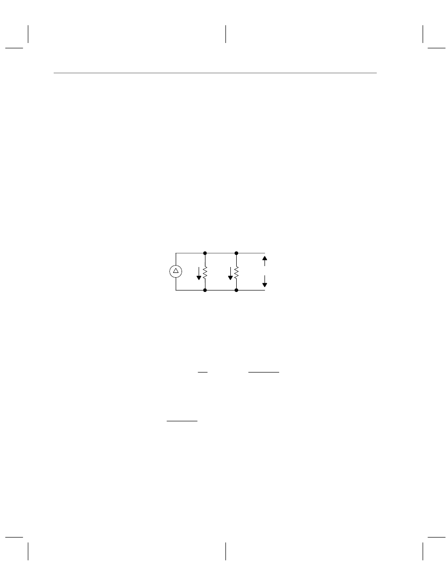
Kirchoff’s current law states: the sum of the currents entering a junction equals the sum
of the currents leaving a junction. It makes no difference if a current flows from a current

Voltage Divider Rule
2-3
Review of Circuit Theory
source, through a component, or through a wire, because all currents are treated identi-
cally. Kirchoff’s current law is illustrated in Figure 2–4 and Equations 2–4 and 2–5.
I4
I3
I1
I2
Figure 2–4. Kirchoff’s Current Law
(2–4)
ȍ
I
IN
+
ȍ
I
OUT
(2–5)
I
1
)
I
2
+
I
3
)
I
4
2.3
Voltage Divider Rule
When the output of a circuit is not loaded, the voltage divider rule can be used to calculate
the circuit’s output voltage. Assume that the same current flows through all circuit ele-
ments (Figure 2–5). Equation 2–6 is written using Ohm’s law as V = I (R
1
+ R
2
). Equation
2–7 is written as Ohm’s law across the output resistor.
V
R2
I
VO
R1
I
Figure 2–5. Voltage Divider Rule
(2–6)
I
+
V
R
1
)
R
2
(2–7)
V
OUT
+
IR
2
Substituting Equation 2–6 into Equation 2–7, and using algebraic manipulation yields
Equation 2–8.
(2–8)
V
OUT
+
V
R
2
R
1
)
R
2
A simple way to remember the voltage divider rule is that the output resistor is divided by
the total circuit resistance. This fraction is multiplied by the input voltage to obtain the out-
Current Divider Rule
2-4
put voltage. Remember that the voltage divider rule always assumes that the output resis-
tor is not loaded; the equation is not valid when the output resistor is loaded by a parallel
component. Fortunately, most circuits following a voltage divider are input circuits, and
input circuits are usually high resistance circuits. When a fixed load is in parallel with the
output resistor, the equivalent parallel value comprised of the output resistor and loading
resistor can be used in the voltage divider calculations with no error. Many people ignore
the load resistor if it is ten times greater than the output resistor value, but this calculation
can lead to a 10% error.
2.4
Current Divider Rule
When the output of a circuit is not loaded, the current divider rule can be used to calculate
the current flow in the output branch circuit (R
2
). The currents I
1
and I
2
in Figure 2–6 are
assumed to be flowing in the branch circuits. Equation 2–9 is written with the aid of Kirch-
off’s current law. The circuit voltage is written in Equation 2–10 with the aid of Ohm’s law.
Combining Equations 2–9 and 2–10 yields Equation 2–11.
I
R2
V
I2
I1
R1
Figure 2–6. Current Divider Rule
(2–9)
I
+
I
1
)
I
2
(2–10)
V
+
I
1
R
1
+
I
2
R
2
(2–11)
I
+
I
1
)
I
2
+
I
2
R
2
R
1
)
I
2
+
I
2
ǒ
R
1
)
R
2
R
1
Ǔ
Rearranging the terms in Equation 2–11 yields Equation 2–12.
(2–12)
I
2
+
I
ǒ
R
1
R
1
)
R
2
Ǔ
The total circuit current divides into two parts, and the resistance (R
1
) divided by the total
resistance determines how much current flows through R
2
. An easy method of remember-
ing the current divider rule is to remember the voltage divider rule. Then modify the voltage
divider rule such that the opposite resistor is divided by the total resistance, and the frac-
tion is multiplied by the input current to get the branch current.

Thevenin’s Theorem
2-5
Review of Circuit Theory
2.5
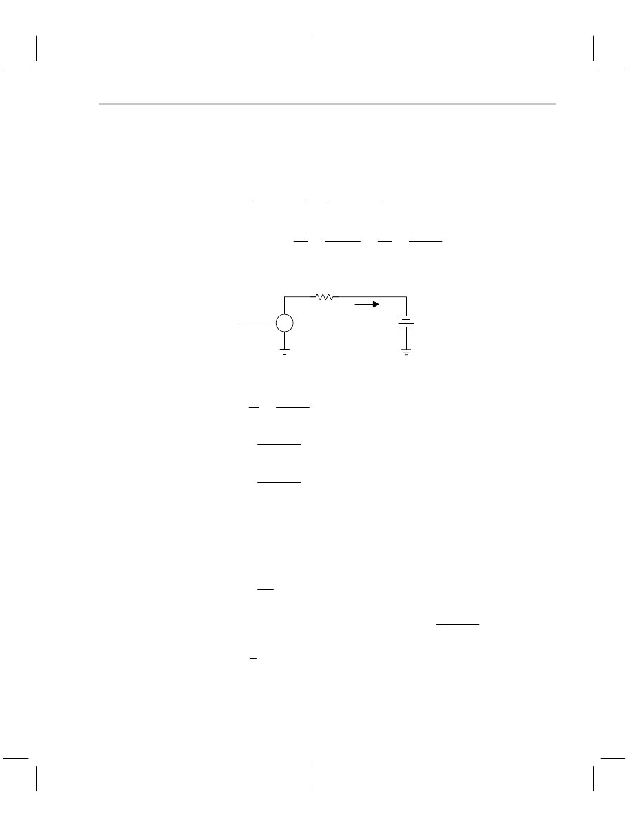
Thevenin’s Theorem
There are times when it is advantageous to isolate a part of the circuit to simplify the analy-
sis of the isolated part of the circuit. Rather than write loop or node equations for the com-
plete circuit, and solving them simultaneously, Thevenin’s theorem enables us to isolate
the part of the circuit we are interested in. We then replace the remaining circuit with a
simple series equivalent circuit, thus Thevenin’s theorem simplifies the analysis.
There are two theorems that do similar functions. The Thevenin theorem just described
is the first, and the second is called Norton’s theorem. Thevenin’s theorem is used when
the input source is a voltage source, and Norton’s theorem is used when the input source
is a current source. Norton’s theorem is rarely used, so its explanation is left for the reader
to dig out of a textbook if it is ever required.
The rules for Thevenin’s theorem start with the component or part of the circuit being re-
placed. Referring to Figure 2–7, look back into the terminals (left from C and R
3
toward
point XX in the figure) of the circuit being replaced. Calculate the no load voltage (V
TH
)
as seen from these terminals (use the voltage divider rule).
V
R3
C
R1
R2
X
X
Figure 2–7. Original Circuit
Look into the terminals of the circuit being replaced, short independent voltage sources,
and calculate the impedance between these terminals. The final step is to substitute the
Thevenin equivalent circuit for the part you wanted to replace as shown in Figure 2–8.
VTH
R3
C
RTH
X
X
Figure 2–8. Thevenin’s Equivalent Circuit for Figure 2–7
The Thevenin equivalent circuit is a simple series circuit, thus further calculations are sim-
plified. The simplification of circuit calculations is often sufficient reason to use Thevenin’s

Thevenin’s Theorem
2-6
theorem because it eliminates the need for solving several simultaneous equations. The
detailed information about what happens in the circuit that was replaced is not available
when using Thevenin’s theorem, but that is no consequence because you had no interest
in it.
As an example of Thevenin’s theorem, let’s calculate the output voltage (V
OUT
) shown in
Figure 2–9A. The first step is to stand on the terminals X–Y with your back to the output
circuit, and calculate the open circuit voltage seen (V
TH
). This is a perfect opportunity to
use the voltage divider rule to obtain Equation 2–13.
V
VOUT
R2
R1
R3
X
Y
(a) The Original Circuit
VTH
VOUT
RTH
R3
X
Y
(b) The Thevenin Equivalent Circuit
R4
R4
Figure 2–9. Example of Thevenin’s Equivalent Circuit
(2–13)
V
TH
+
V
R
2
R
1
)
R
2
Still standing on the terminals X-Y, step two is to calculate the impedance seen looking
into these terminals (short the voltage sources). The Thevenin impedance is the parallel
impedance of R
1
and R
2
as calculated in Equation 2–14. Now get off the terminals X-Y
before you damage them with your big feet. Step three replaces the circuit to the left of
X-Y with the Thevenin equivalent circuit V
TH
and R
TH
.
(2–14)
R
TH
+
R
1
R
2
R
1
)
R
2
+
R
1
Ŧ
R
2
Note:
Two parallel vertical bars ( || ) are used to indicate parallel components as
shown in Equation 2–14.
The final step is to calculate the output voltage. Notice the voltage divider rule is used
again. Equation 2–15 describes the output voltage, and it comes out naturally in the form
of a series of voltage dividers, which makes sense. That’s another advantage of the volt-
age divider rule; the answers normally come out in a recognizable form rather than a
jumble of coefficients and parameters.

Thevenin’s Theorem
2-7
Review of Circuit Theory
(2–15)
V
OUT
+
V
TH
R
4
R
TH
)
R
3
)
R
4
+
V
ǒ
R
2
R
1
)
R
2
Ǔ
R
4
R
1
R
2
R
1
)
R
2
)
R
3
)
R
4
The circuit analysis is done the hard way in Figure 2–10, so you can see the advantage
of using Thevenin’s Theorem. Two loop currents, I
1
and I
2
, are assigned to the circuit.
Then the loop Equations 2–16 and 2–17 are written.
V
R3
VOUT
I1
R1
I2
R4
R2
Figure 2–10. Analysis Done the Hard Way
(2–16)
V
+
I
1
ǒ
R
1
)
R
2
Ǔ
*
I
2
R
2
(2–17)
I
2
ǒ
R
2
)
R
3
)
R
4
Ǔ
+
I
1
R
2
Equation 2–17 is rewritten as Equation 2–18 and substituted into Equation 2–16 to obtain
Equation 2–19.
(2–18)
I
1
+
I
2
R
2
)
R
3
)
R
4
R
2
(2–19)
V
+
I
2
ǒ
R
2
)
R
3
)
R
4
R
2
Ǔ
ǒ
R
1
)
R
2
Ǔ
*
I
2
R
2
The terms are rearranged in Equation 2–20. Ohm’s law is used to write Equation 2–21,
and the final substitutions are made in Equation 2–22.
(2–20)
I
2
+
V
R
2
)
R
3
)
R
4
R
2
ǒ
R
1
)
R
2
Ǔ
*
R
2
(2–21)
V
OUT
+
I
2
R
4
(2–22)
V
OUT
+
V
R
4
ǒ
R
2
)
R
3
)
R
4
Ǔ ǒ
R
1
)
R
2
Ǔ
R
2
*
R
2
This is a lot of extra work for no gain. Also, the answer is not in a usable form because
the voltage dividers are not recognizable, thus more algebra is required to get the answer
into usable form.

Superposition
2-8
2.6
Superposition
Superposition is a theorem that can be applied to any linear circuit. Essentially, when
there are independent sources, the voltages and currents resulting from each source can
be calculated separately, and the results are added algebraically. This simplifies the cal-
culations because it eliminates the need to write a series of loop or node equations. An
example is shown in Figure 2–11.
V1
VOUT
R1
R2
R3
V2
Figure 2–11.Superposition Example
When V
1
is grounded, V
2
forms a voltage divider with R
3
and the parallel combination of
R
2
and R
1
. The output voltage for this circuit (V
OUT2
) is calculated with the aid of the volt-
age divider equation (2–23). The circuit is shown in Figure 2–12. The voltage divider rule
yields the answer quickly.
V2
VOUT2
R3
R2
R1
Figure 2–12. When V
1
is Grounded
(2–23)
V
OUT2
+
V
2
R
1
ø
R
2
R
3
)
R
1
ø
R
2
Likewise, when V
2
is grounded (Figure 2–13), V
1
forms a voltage divider with R
1
and the
parallel combination of R
3
and R
2
, and the voltage divider theorem is applied again to cal-
culate V
OUT
(Equation 2–24).
V1
VOUT1
R1
R2
R3
Figure 2–13. When V
2
is Grounded

Calculation of a Saturated Transistor Circuit
2-9
Review of Circuit Theory
(2–24)
V
OUT1
+
V
1
R
2
ø
R
3
R
1
)
R
2
ø
R
3
After the calculations for each source are made the components are added to obtain the
final solution (Equation 2–25).
(2–25)
V
OUT
+
V
1
R
2
ø
R
3
R
1
)
R
2
ø
R
3
)
V
2
R
1
ø
R
2
R
3
)
R
1
ø
R
2
The reader should analyze this circuit with loop or node equations to gain an appreciation
for superposition. Again, the superposition results come out as a simple arrangement that
is easy to understand. One looks at the final equation and it is obvious that if the sources
are equal and opposite polarity, and when R
1
= R
3
, then the output voltage is zero. Conclu-
sions such as this are hard to make after the results of a loop or node analysis unless con-
siderable effort is made to manipulate the final equation into symmetrical form.
2.7
Calculation of a Saturated Transistor Circuit
The circuit specifications are: when V
IN
= 12 V, V
OUT
<0.4 V at I
SINK
<10 mA, and V
IN
<0.05
V, V
OUT
>10 V at I
OUT
= 1 mA. The circuit diagram is shown in Figure 2–14.
IC
12 V
VOUT
IB
RB
VIN
RC
Figure 2–14. Saturated Transistor Circuit
The collector resistor must be sized (Equation 2–26) when the transistor is off, because
it has to be small enough to allow the output current to flow through it without dropping
more than two volts to meet the specification for a 10-V output.
(2–26)
R
C
v
V
)
12
*
V
OUT
I
OUT
+
12
*
10
1
+
2 k
When the transistor is off, 1 mA can be drawn out of the collector resistor without pulling
the collector or output voltage to less than ten volts (Equation 2–27). When the transistor
is on, the base resistor must be sized (Equation 2–28) to enable the input signal to drive
enough base current into the transistor to saturate it. The transistor beta is 50.
Transistor Amplifier
2-10
(2–27)
I
C
+ b
I
B
+
V
)
12
*
V
CE
R
C
)
I
L
[
V
)
12
R
C
)
I
L
(2–28)
R
B
v
V
IN
*
V
BE
I
B
Substituting Equation 2–27 into Equation 2–28 yields Equation 2–29.
(2–29)
R
B
v
ǒ
V
IN
*
V
BE
Ǔ
b
I
C
+
(12
*
0.6) 50 V
ƪ
12
2
)
(10)
ƫ
mA
+
35.6 k
When the transistor goes on it sinks the load current, and it still goes into saturation. These
calculations neglect some minor details, but they are in the 98% accuracy range.
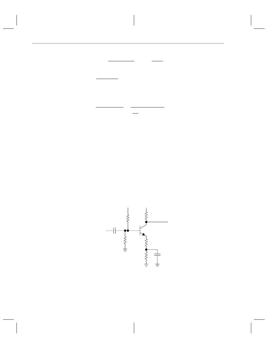
2.8
Transistor Amplifier
The amplifier is an analog circuit (Figure 2–15), and the calculations, plus the points that
must be considered during the design, are more complicated than for a saturated circuit.
This extra complication leads people to say that analog design is harder than digital de-
sign (the saturated transistor is digital i.e.; on or off). Analog design is harder than digital
design because the designer must account for all states in analog, whereas in digital only
two states must be accounted for. The specifications for the amplifier are an ac voltage
gain of four and a peak-to-peak signal swing of 4 volts.
12 V
VOUT
VIN
RC
CE
RE2
RE1
R1
R2
12 V
CIN
Figure 2–15. Transistor Amplifier
I
C
is selected as 10 mA because the transistor has a current gain (
β
) of 100 at that point.
The collector voltage is arbitrarily set at 8 V; when the collector voltage swings positive
Transistor Amplifier
2-11
Review of Circuit Theory
2 V (from 8 V to 10 V) there is still enough voltage dropped across R
C
to keep the transistor
on. Set the collector-emitter voltage at 4 V; when the collector voltage swings negative
2 V (from 8 V to 6 V) the transistor still has 2 V across it, so it stays linear. This sets the
emitter voltage (V
E
) at 4 V.
(2–30)
R
C
v
V
)
12
*
V
C
I
C
+
12 V
*
8 V
10 mA
+
400
W
(2–31)
R
E
+
R
E1
)
R
E2
+
V
E
I
E
+
V
E
I
B
)
I
C
^
V
E
I
C
+
4 V
10 mA
+
400
W
Use Thevenin’s equivalent circuit to calculate R
1
and R
2
as shown in Figure 2–16.
IB
R1 || R2
VB = 4.6 V
R2
R1 + R2
12
Figure 2–16. Thevenin Equivalent of the Base Circuit
(2–32)
I
B
+
I
C
b +
10 mA
100
+
0.1 mA
(2–33)
V
TH
+
12R
2
R
1
)
R
2
(2–34)
R
TH
+
R
1
R
2
R
1
)
R
2
We want the base voltage to be 4.6 V because the emitter voltage is then 4 V. Assume
a voltage drop of 0.4 V across R
TH
, so Equation 2–35 can be written. The drop across R
TH
may not be exactly 0.4 V because of beta variations, but a few hundred mV does not mat-
ter is this design. Now, calculate the ratio of R
1
and R
2
using the voltage divider rule (the
load current has been accounted for).
(2–35)
R
TH
+
0.4
0.1
k
+
4 k
(2–36)
V
TH
+
I
B
R
Th
)
V
B
+
0.4
)
4.6
+
5
+
12
R
2
R
1
)
R
2
(2–37)
R
2
+
7
5
R
1
R
1
is almost equal to R
2
, thus selecting R
1
as twice the Thevenin resistance yields approx-
imately 4 K as shown in Equation 2–35. Hence, R
1
= 11.2 k and R
2
= 8 k. The ac gain is

Transistor Amplifier
2-12
approximately R
C
/R
E1
because C
E
shorts out R
E2
at high frequencies, so we can write
Equation 2–38.
(2–38)
R
E1
+
R
C
G
+
400
4
+
100
W
(2–39)
R
E2
+
R
E
*
R
E1
+
400
*
100
+
300
W
The capacitor selection depends on the frequency response required for the amplifier, but
10
µ
F for C
IN
and 1000
µ
F for C
E
suffice for a starting point.

IMPORTANT NOTICE
Texas Instruments Incorporated and its subsidiaries (TI) reserve the right to make corrections, modifications,
enhancements, improvements, and other changes to its products and services at any time and to discontinue
any product or service without notice. Customers should obtain the latest relevant information before placing
orders and should verify that such information is current and complete. All products are sold subject to TI’s terms
and conditions of sale supplied at the time of order acknowledgment.
TI warrants performance of its hardware products to the specifications applicable at the time of sale in
accordance with TI’s standard warranty. Testing and other quality control techniques are used to the extent TI
deems necessary to support this warranty. Except where mandated by government requirements, testing of all
parameters of each product is not necessarily performed.
TI assumes no liability for applications assistance or customer product design. Customers are responsible for
their products and applications using TI components. To minimize the risks associated with customer products
and applications, customers should provide adequate design and operating safeguards.
TI does not warrant or represent that any license, either express or implied, is granted under any TI patent right,
copyright, mask work right, or other TI intellectual property right relating to any combination, machine, or process
in which TI products or services are used. Information published by TI regarding third–party products or services
does not constitute a license from TI to use such products or services or a warranty or endorsement thereof.
Use of such information may require a license from a third party under the patents or other intellectual property
of the third party, or a license from TI under the patents or other intellectual property of TI.
Reproduction of information in TI data books or data sheets is permissible only if reproduction is without
alteration and is accompanied by all associated warranties, conditions, limitations, and notices. Reproduction
of this information with alteration is an unfair and deceptive business practice. TI is not responsible or liable for
such altered documentation.
Resale of TI products or services with statements different from or beyond the parameters stated by TI for that
product or service voids all express and any implied warranties for the associated TI product or service and
is an unfair and deceptive business practice. TI is not responsible or liable for any such statements.
Mailing Address:
Texas Instruments
Post Office Box 655303
Dallas, Texas 75265
Copyright
2001, Texas Instruments Incorporated
Wyszukiwarka
Podobne podstrony:
Review of Wahl&Amman
Grzegorz Ziółkowski Review of MEN IN BLACK
Notes on the?onomics of Game Theory
Book Review of The Color Purple
A Review of The Outsiders Club Screened on?C 2 in October
A review of molecular techniques to type C glabrata isolates
Short review of the book entitled E for?stasy
F J Yndurain Elements of Group Theory
Lamarcks Influence on the?velopment Of?rwins Theory Of E
Book Review of The Burning Man
SHSBC403 A Review of Study
Part8 Review of Objectives, Points to Remember
Outline of Relevance Theory
więcej podobnych podstron