
Chapter 6
Development of the Non Ideal Op Amp Equations
Literature Number SLOA078
Excerpted from
Op Amps for Everyone
Literature Number: SLOD006A

6-1
Development of the Non Ideal Op Amp
Equations
Ron Mancini
6.1
Introduction
There are two types of error sources in op amps, and they fall under the general classifica-
tion of dc and ac errors. Examples of dc errors are input offset voltage and input bias cur-
rent. The dc errors stay constant over the usable op amp frequency range; therefore, the
input bias current is 10 pA at 1 kHz and it is 10 pA at 10 kHz. Because of their constant
and controlled behavior, dc errors are not considered until later chapters.
AC errors are flighty, so we address them here by developing a set of nonideal equations
that account for ac errors. The ac errors may show up under dc conditions, but they get
worse as the operating frequency increases. A good example of an ac error is common–
mode rejection ration (CMRR). Most op amps have a guaranteed CMRR specification,
but this specification is only valid at dc or very low frequencies. Further inspection of the
data sheet reveals that CMRR decreases as operating frequency increases. Several oth-
er specifications that fall into the category of ac specifications are output impedance,
power-supply rejection-ratio, peak-to-peak output voltage, differential gain, differential
phase, and phase margin.
Differential gain is the most important ac specification because the other ac specifications
are derived from the differential gain. Until now, differential gain has been called op amp
gain or op amp open loop gain, and we shall continue with that terminology. Let the data
sheet call it differential gain.
As shown in prior chapters, when frequency increases, the op amp gain decreases and
errors increase. This chapter develops the equations that illustrate the effects of the gain
changes. We start with a review of the basic canonical feedback system stability because
the op amp equations are developed using the same techniques.
Amplifiers are built with active components such as transistors. Pertinent transistor pa-
rameters like transistor gain are subject to drift and initial inaccuracies from many
sources, so amplifiers being built from these components are subject to drift and inaccura-
Chapter 6
Review of the Canonical Equations
6-2
cies. The drift and inaccuracy is minimized or eliminated by using negative feedback. The
op amp circuit configuration employs feedback to make the transfer equation of the circuit
independent of the amplifier parameters (well almost), and while doing this, the circuit
transfer function is made dependent on external passive components. The external pas-
sive components can be purchased to meet almost any drift or accuracy specification;
only the cost and size of the passive components limit their use.
Once feedback is applied to the op amp it is possible for the op amp circuit to become
unstable. Certain amplifiers belong to a family called internally compensated op amps;
they contain internal capacitors that are sometimes advertised as precluding instabilities.
Although internally compensated op amps should not oscillate when operated under spe-
cified conditions, many have relative stability problems that manifest themselves as poor
phase response, ringing, and overshoot. The only absolutely stable internally compen-
sated op amp is the one lying on the workbench without power applied! All other internally
compensated op amps oscillate under some external circuit conditions.
Noninternally compensated or externally compensated op amps are unstable without the
addition of external stabilizing components. This situation is a disadvantage in many
cases because they require additional components, but the lack of internal compensation
enables the top-drawer circuit designer to squeeze the last drop of performance from the
op amp. You have two options: op amps internally compensated by the IC manufacturer,
or op amps externally compensated by you. Compensation, except that done by the op
amp manufacturer, must be done external to the IC. Surprisingly enough, internally com-
pensated op amps require external compensation for demanding applications.
Compensation is achieved by adding external components that modify the circuit transfer
function so that it becomes unconditionally stable. There are several different methods
of compensating an op amp, and as you might suspect, there are pros and cons
associated with each method of compensation. After the op amp circuit is compensated,
it must be analyzed to determine the effects of compensation. The modifications that com-
pensation have on the closed loop transfer function often determine which compensation
scheme is most profitably employed.
6.2
Review of the Canonical Equations
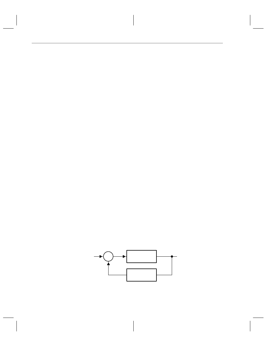
A block diagram for a generalized feedback system is repeated in Figure 6–1. This simple
block diagram is sufficient to determine the stability of any system.
A
β
Σ
+
–
VIN
VOUT
E
Figure 6–1. Feedback System Block Diagram

Review of the Canonical Equations
6-3
Development of the Non Ideal Op Amp Equations
The output and error equation development is repeated below.
(6–1)
V
OUT
+
EA
(6–2)
E
+
V
IN
* b
V
OUT
Combining Equations 6–1 and 6–2 yields Equation 6–3:
(6–3)
V
OUT
A
+
V
IN
* b
V
OUT
Collecting terms yields Equation 6–4:
(6–4)
V
OUT
ǒ
1
A
) b
Ǔ
+
V
IN
Rearranging terms yields the classic form of the feedback equation.
(6–5)
V
OUT
V
IN
+
A
1
)
A
b
Notice that Equation 6–5 reduces to Equation 6–6 when the quantity A
β
in Equation 6–5
becomes very large with respect to one. Equation 6–6 is called the ideal feedback equa-
tion because it depends on the assumption that A
β
>> 1, and it finds extensive use when
amplifiers are assumed to have ideal qualities. Under the conditions that A
β
>>1, the sys-
tem gain is determined by the feedback factor
β.
Stable passive circuit components are
used to implement the feedback factor, thus the ideal closed loop gain is predictable and
stable because
β
is predictable and stable.
(6–6)
V
OUT
V
IN
+
1
b
The quantity A
β
is so important that it has been given a special name, loop gain. Consider
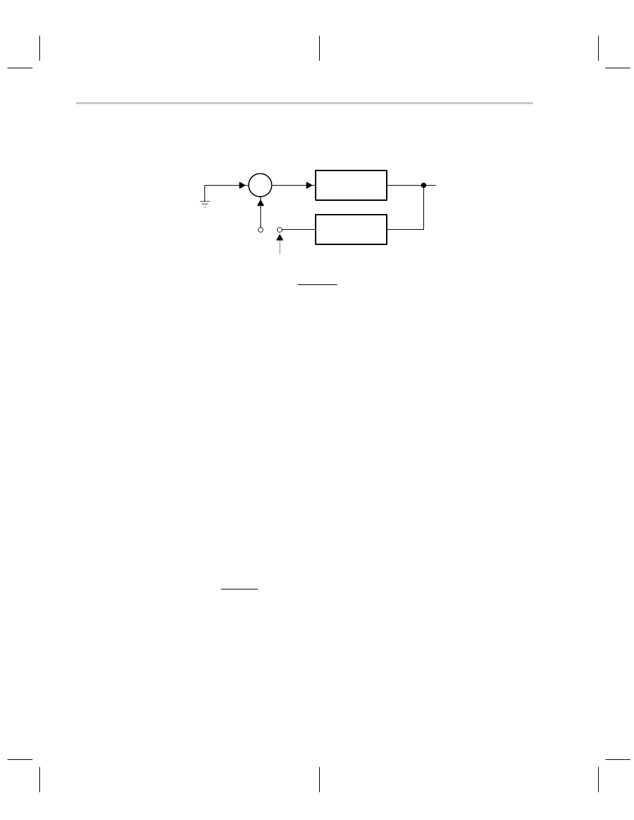
Figure 6–2; when the voltage inputs are grounded (current inputs are opened) and the
loop is broken, the calculated gain is the loop gain, A
β.
Now, keep in mind that this is a
mathematics of complex numbers, which have magnitude and direction. When the loop
gain approaches minus one, or to express it mathematically
1
∠
–180
°
, Equation 6–5 ap-
proaches infinity because 1/0
⇒ ∞
.
The circuit output heads for infinity as fast as it can
Review of the Canonical Equations
6-4
using the equation of a straight line. If the output were not energy limited the circuit would
explode the world, but it is energy limited by the power supplies so the world stays intact.
A
β
Σ
+
–
AVTEST
VTEST
VRETURN
VTEST
VRETURN
= A
β
Figure 6–2. Feedback Loop Broken to Calculate Loop Gain
Active devices in electronic circuits exhibit nonlinear behavior when their output ap-
proaches a power supply rail, and the nonlinearity reduces the amplifier gain until the loop
gain no longer equals
1
∠
–180
°
. Now the circuit can do two things: first, it could become
stable at the power supply limit, or second, it can reverse direction (because stored
charge keeps the output voltage changing) and head for the negative power supply rail.
The first state where the circuit becomes stable at a power supply limit is named lockup;
the circuit will remain in the locked up state until power is removed. The second state
where the circuit bounces between power supply limits is named oscillatory. Remember,
the loop gain, A
β
, is the sole factor that determines stability for a circuit or system. Inputs
are grounded or disconnected when the loop gain is calculated, so they have no effect
on stability. The loop gain criteria is analyzed in depth later.
Equations 6–1 and 6–2 are combined and rearranged to yield Equation 6–7, which gives
an indication of system or circuit error.
(6–7)
E
+
V
IN
1
)
A
b
First, notice that the error is proportional to the input signal. This is the expected result
because a bigger input signal results in a bigger output signal, and bigger output signals
require more drive voltage. Second, the loop gain is inversely proportional to the error.
As the loop gain increases the error decreases, thus large loop gains are attractive for
minimizing errors. Large loop gains also decrease stability, thus there is always a tradeoff
between error and stability.
Noninverting Op Amps
6-5
Development of the Non Ideal Op Amp Equations
6.3
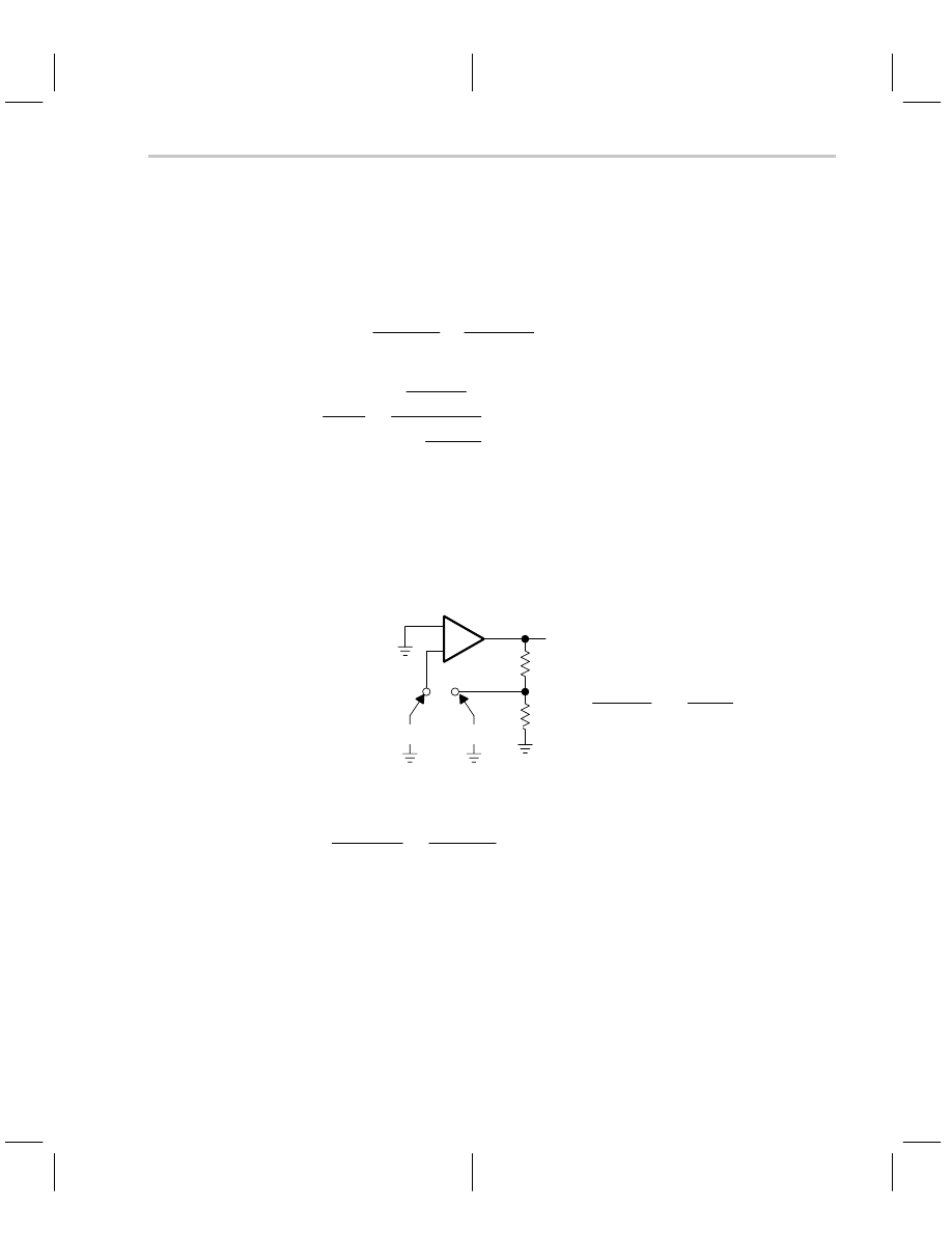
Noninverting Op Amps
A noninverting op amp is shown in Figure 6–3. The dummy variable, V
B
, is inserted to
make the calculations easier and a is the op amp gain.
_
+
VIN
VOUT
ZF
ZG
VB
a
Figure 6–3. Noninverting Op Amp
Equation 6–8 is the amplifier transfer equation.
(6–8)
V
OUT
+
a
ǒ
V
IN
*
V
B
Ǔ
The output equation is developed with the aid of the voltage divider rule. Using the voltage
divider rule assumes that the op amp impedance is low.
(6–9)
V
B
+
V
OUT
Z
G
Z
F
)
Z
G
for I
B
+
0
Combining Equations 6–8 and 6–9 yields Equation 6–10.
(6–10)
V
OUT
+
aV
IN
*
a Z
G
V
OUT
Z
G
)
Z
F
Rearranging terms in Equation 6–10 yields Equation 6–11, which describes the transfer
function of the circuit.
(6–11)
V
OUT
V
IN
+
a
1
)
aZ
G
Z
G
)
Z
F
Equation 6–5 is repeated as Equation 6–12 to make a term by term comparison of the
equations easy.
(6–12)
V
OUT
V
IN
+
A
1
)
A
β
By virtue of the comparison we get Equation 6–13, which is the loop-gain equation for the
noninverting op amp. The loop-gain equation determines the stability of the circuit. The
Inverting Op Amps
6-6
comparison also shows that the open loop gain, A, is equal to the op amp open loop gain,
a, for the noninverting circuit.
(6–13)
A
b +
aZ
G
Z
G
)
Z
F
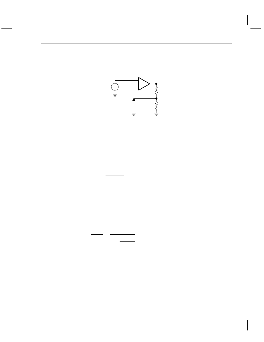
Equation 6–13 is also derived with the aid of Figure 6–4, which shows the open loop non-
inverting op amp.
_
+
aVTEST
ZF
ZG
a
VRETURN
VTEST
Figure 6–4. Open Loop Noninverting Op Amp
The test voltage, V
TEST
, is multiplied by the op amp open loop gain to obtain the op amp
output voltage, aV
TEST
. The voltage divider rule is used to calculate Equation 6–15, which
is identical to Equation 6–14 after some algebraic manipulation.
(6–14)
V
RETURN
+
aV
TEST
Z
G
Z
F
)
Z
G
(6–15)
V
RETURN
V
TEST
+
A
b +
aZ
G
Z
F
)
Z
G
6.4
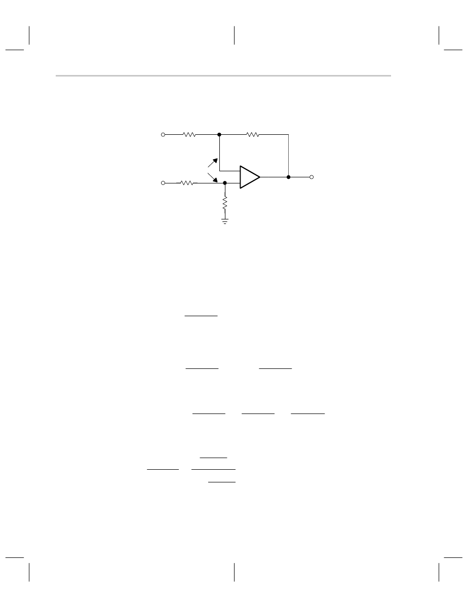
Inverting Op Amps
The inverting op amp circuit is shown in Figure 6–5. The dummy variable (V
A
) is inserted
to make the calculations easier, and a is the op amp open loop gain.
_
+
IB
VIN
VOUT
ZF
ZG
VA
a
Figure 6–5. Inverting Op Amp
Inverting Op Amps
6-7
Development of the Non Ideal Op Amp Equations
The transfer equation is given in Equation 6–16:
(6–16)
V
OUT
+ *
aV
A
The node voltage (Equation 6–17) is obtained with the aid of superposition and the volt-
age divider rule. Equation 6–18 is obtained by combining Equations 6–16 and 6–17.
(6–17)
V
A
+
V
IN
Z
F
Z
G
)
Z
F
)
V
OUT
Z
G
Z
G
)
Z
F
for I
B
+
0
(6–18)
V
OUT
V
IN
+
–aZ
F
Z
G
)
Z
F
1
)
aZ
G
Z
G
)
Z
F
Equation 6–16 is the transfer function of the inverting op amp. By virtue of the comparison
between Equations 6–18 and 6–14, we get Equation 6–15 again, which is also the loop
gain equation for the inverting op amp circuit. The comparison also shows that the open
loop gain (A) is different from the op amp open loop gain (a) for the noninverting circuit.
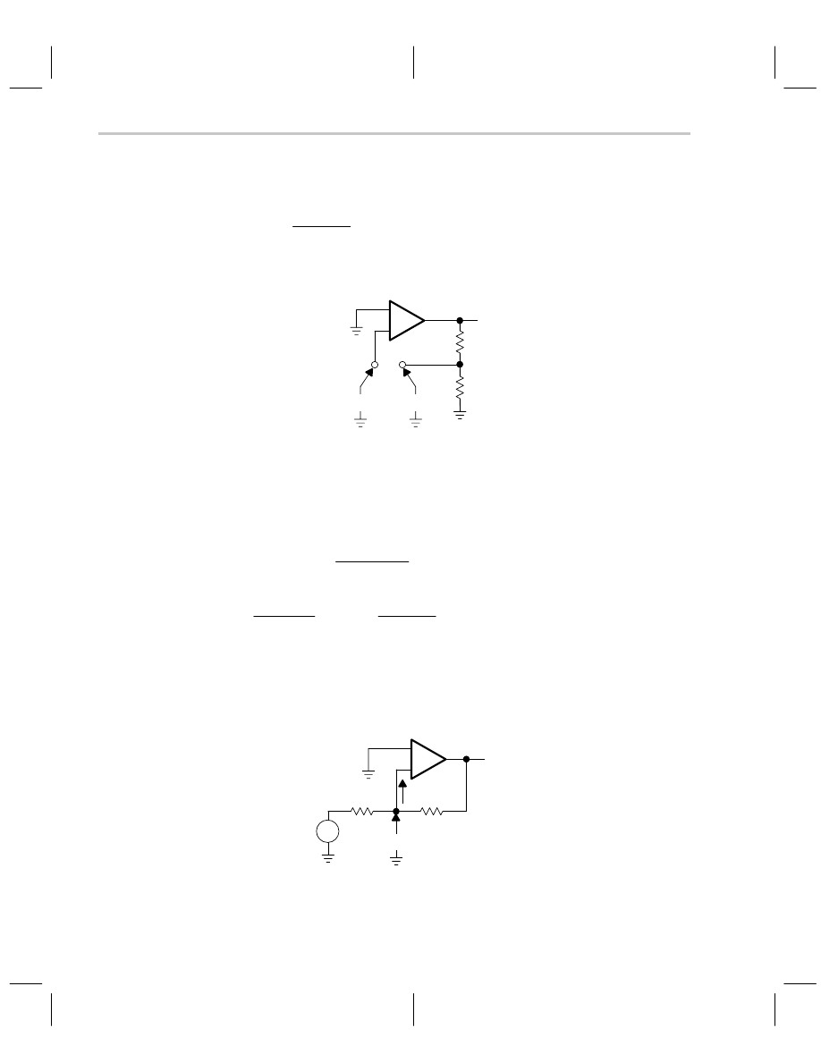
The inverting op amp with the feedback loop broken is shown in Figure 6–6, and this circuit
is used to calculate the loop-gain given in Equation 6–19.
_
+
VOUT
ZF
ZG
a
VRETURN
VTEST
VTEST
VRETURN
= a
ZF + ZG
ZG
Figure 6–6. Inverting Op Amp: Feedback Loop Broken for Loop Gain Calculation
(6–19)
V
RETURN
V
TEST
+
aZ
G
Z
G
)
Z
F
+
A
b
Several things must be mentioned at this point in the analysis. First, the transfer functions
for the noninverting and inverting Equations, 6–13 and 6–18, are different. For a common
set of Z
G
and Z
F
values, the magnitude and polarity of the gains are different. Second,
the loop gain of both circuits, as given by Equations 6–15 and 6–19, is identical. Thus,
the stability performance of both circuits is identical although their transfer equations are
different. This makes the important point that stability is not dependent on the circuit in-
puts. Third, the A gain block shown in Figure 6–1 is different for each op amp circuit. By
comparison of Equations 6–5, 6–11, and 6–18 we see that A
NON–INV
= a and A
INV
= aZ
F
÷
(Z
G
+ Z
F
).
Differential Op Amps
6-8
6.5
Differential Op Amps
The differential amplifier circuit is shown in Figure 6–7. The dummy variable, V
E
, is in-
serted to make the calculations easier, and a is the open loop gain.
_
+
ZF
VOUT
ZG
VE
ZF
ZG
V–
V+
a
V1
V2
Figure 6–7. Differential Amplifier Circuit
Equation 6–20 is the circuit transfer equation.
(6–20)
V
OUT
+
a V
E
+
V
)
*
V
*
The positive input voltage, V
+
, is written in Equation 6–21 with the aid of superposition and
the voltage divider rule.
(6–21)
V
)
+
V
2
Z
F
Z
F
)
Z
G
The negative input voltage, V
–
, is written in Equation 6–22 with the aid of superposition
and the voltage divider rule.
(6–22)
V
*
+
V
1
Z
F
Z
F
)
Z
G
*
V
OUT
Z
G
Z
F
)
Z
G
Combining Equations 6–20, 6–21, and 6–22 yields Equation 6–23.
(6–23)
V
OUT
+
a
ƪ
V
2
Z
F
Z
F
)
Z
G
*
V
1
Z
F
Z
F
)
Z
G
*
V
OUT
Z
G
Z
F
)
Z
G
ƫ
After algebraic manipulation, Equation 6–23 reduces to Equation 6–24.
(6–24)
V
OUT
V
2
*
V
1
+
aZ
F
Z
F
)
Z
G
1
)
a Z
G
Z
F
)
Z
G
The comparison method reveals that the loop gain as shown in Equation 6–25 is identical
to that shown in Equations 6–13 and 6–19.

Differential Op Amps
6-9
Development of the Non Ideal Op Amp Equations
(6–25)
A
b +
aZ
G
Z
G
)
Z
F
Again, the loop gain, which determines stability, is only a function of the closed loop, and
independent of the inputs.

6-10

IMPORTANT NOTICE
Texas Instruments Incorporated and its subsidiaries (TI) reserve the right to make corrections, modifications,
enhancements, improvements, and other changes to its products and services at any time and to discontinue
any product or service without notice. Customers should obtain the latest relevant information before placing
orders and should verify that such information is current and complete. All products are sold subject to TI’s terms
and conditions of sale supplied at the time of order acknowledgment.
TI warrants performance of its hardware products to the specifications applicable at the time of sale in
accordance with TI’s standard warranty. Testing and other quality control techniques are used to the extent TI
deems necessary to support this warranty. Except where mandated by government requirements, testing of all
parameters of each product is not necessarily performed.
TI assumes no liability for applications assistance or customer product design. Customers are responsible for
their products and applications using TI components. To minimize the risks associated with customer products
and applications, customers should provide adequate design and operating safeguards.
TI does not warrant or represent that any license, either express or implied, is granted under any TI patent right,
copyright, mask work right, or other TI intellectual property right relating to any combination, machine, or process
in which TI products or services are used. Information published by TI regarding third–party products or services
does not constitute a license from TI to use such products or services or a warranty or endorsement thereof.
Use of such information may require a license from a third party under the patents or other intellectual property
of the third party, or a license from TI under the patents or other intellectual property of TI.
Reproduction of information in TI data books or data sheets is permissible only if reproduction is without
alteration and is accompanied by all associated warranties, conditions, limitations, and notices. Reproduction
of this information with alteration is an unfair and deceptive business practice. TI is not responsible or liable for
such altered documentation.
Resale of TI products or services with statements different from or beyond the parameters stated by TI for that
product or service voids all express and any implied warranties for the associated TI product or service and
is an unfair and deceptive business practice. TI is not responsible or liable for any such statements.
Mailing Address:
Texas Instruments
Post Office Box 655303
Dallas, Texas 75265
Copyright
2001, Texas Instruments Incorporated
Wyszukiwarka
Podobne podstrony:
94 Development of the Ideal Op Amp Equations
EFFECTS OF CAFFEINE AND AMINOPHYLLINE ON ADULT DEVELOPMENT OF THE CECROPIA
Jakobsson, The Taxonomy of the Non Existent Some M
The Development of the Case System in French
The development of the English novel in the 18th century
9 The development of the English novel in the 18th century
Rick Strassman Subjective effects of DMT and the development of the Hallucinogen Rating Scale
Brzechczyn, Krzysztof In the Trap of Post Socialist Stagnation On Political Development of the Bela
Genesis for the New Space Age Secret Development of the Round Wing Plane the Extra Terrestrials Ins
1 Development of the Lithium Ion Battery and Recent T 2014 Lithium Ion Bat
Andersson, T Displacement of the Heroic Ideal in the Family Sagas
Invention And Development Of The Flag Antenna
Brzechczyn, Krzysztof On the Application of non Marxian Historical Materialism to the Development o
fitopatologia, Microarrays are one of the new emerging methods in plant virology currently being dev
Aristoteles # Guthrie (The Development of Aristotle's Theology 1) BB
An experimental study on the development of a b type Stirling engine
więcej podobnych podstron