BD243, BD243A, BD243B, BD243C
NPN SILICON POWER TRANSISTORS
1
JUNE 1973 - REVISED SEPTEMBER 2002
Specifications are subject to change without notice.
●
Designed for Complementary Use with the
BD244 Series
●
65 W at 25°C Case Temperature
●
6 A Continuous Collector Current
●
10 A Peak Collector Current
●
Customer-Specified Selections Available
absolute maximum ratings at 25°C case temperature (unless otherwise noted)
NOTES: 1. This value applies for t
p
≤ 0.3 ms, duty cycle ≤ 10%.
2. Derate linearly to 150°C case temperature at the rate of 0.52 W/°C.
3. Derate linearly to 150°C free air temperature at the rate of 16 mW/°C.
4. This rating is based on the capability of the transistor to operate safely in a circuit of: L = 20 mH, I
B(on)
= 0.4 A, R
BE
= 100
Ω,
V
BE(off)
= 0, R
S
= 0.1
Ω, V
CC
= 20 V.
RATING
SYMBOL
VALUE
UNIT
Collector-emitter voltage (R
BE
= 100
Ω)
BD243
BD243A
BD243B
BD243C
V
CER
55
70
90
115
V
Collector-emitter voltage (I
C
= 30 mA)
BD243
BD243A
BD243B
BD243C
V
CEO
45
60
80
100
V
Emitter-base voltage
V
EBO
5
V
Continuous collector current
I
C
6
A
Peak collector current (see Note 1)
I
CM
10
A
Continuous base current
I
B
3
A
Continuous device dissipation at (or below) 25°C case temperature (see Note 2)
P
tot
65
W
Continuous device dissipation at (or below) 25°C free air temperature (see Note 3)
P
tot
2
W
Unclamped inductive load energy (see Note 4)
½LI
C
2
62.5
mJ
Operating junction temperature range
T
j
-65 to +150
°C
Storage temperature range
T
stg
-65 to +150
°C
Lead temperature 3.2 mm from case for 10 seconds
T
L
250
°C
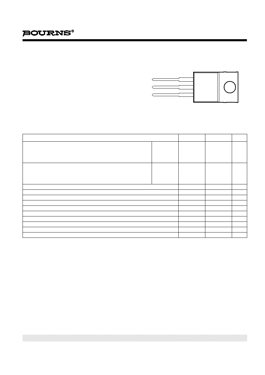
B
C
E
TO-220 PACKAGE
(TOP VIEW)
Pin 2 is in electrical contact with the mounting base.
MDTRACA
1
2
3
BD243, BD243A, BD243B, BD243C
NPN SILICON POWER TRANSISTORS
2
JUNE 1973 - REVISED SEPTEMBER 2002
Specifications are subject to change without notice.
NOTES: 5. These parameters must be measured using pulse techniques, t
p
= 300 µs, duty cycle
≤ 2%.
6. These parameters must be measured using voltage-sensing contacts, separate from the current carrying contacts.
†
Voltage and current values shown are nominal; exact values vary slightly with transistor parameters.
electrical characteristics at 25°C case temperature
PARAMETER
TEST CONDITIONS
MIN
TYP
MAX
UNIT
V
(BR)CEO
Collector-emitter
breakdown voltage
I
C
= 30 mA
(see Note 5)
I
B
= 0
BD243
BD243A
BD243B
BD243C
45
60
80
100
V
I
CES
Collector-emitter
cut-off current
V
CE
= 55 V
V
CE
= 70 V
V
CE
= 90 V
V
CE
= 115 V
V
BE
= 0
V
BE
= 0
V
BE
= 0
V
BE
= 0
BD243
BD243A
BD243B
BD243C
0.4
0.4
0.4
0.4
mA
I
CEO
Collector cut-off
current
V
CE
= 30 V
V
CE
= 60 V
I
B
= 0
I
B
= 0
BD243/243A
BD243B/243C
0.7
0.7
mA
I
EBO
Emitter cut-off
current
V
EB
= 5 V
I
C
= 0
1
mA
h
FE
Forward current
transfer ratio
V
CE
= 4 V
V
CE
= 4 V
I
C
= 0.3 A
I
C
= 3 A
(see Notes 5 and 6)
30
15
V
CE(sat)
Collector-emitter
saturation voltage
I
B
= 1 A
I
C
= 6 A
(see Notes 5 and 6)
1.5
V
V
BE
Base-emitter
voltage
V
CE
= 4 V
I
C
= 6 A
(see Notes 5 and 6)
2
V
h
fe
Small signal forward
current transfer ratio
V
CE
= 10 V
I
C
= 0.5 A
f = 1 kHz
20
|
h
fe
|
Small signal forward
current transfer ratio
V
CE
= 10 V
I
C
= 0.5 A
f = 1 MHz
3
thermal characteristics
PARAMETER
MIN
TYP
MAX
UNIT
R
θJC
Junction to case thermal resistance
1.92
°C/W
R
θJA
Junction to free air thermal resistance
62.5
°C/W
resistive-load-switching characteristics at 25°C case temperature
PARAMETER
TEST CONDITIONS
†
MIN
TYP
MAX
UNIT
t
on
Turn-on time
I
C
= 1 A
V
BE(off)
= -3.7 V
I
B(on)
= 0.1 A
R
L
= 20
Ω
I
B(off)
= -0.1 A
t
p
= 20 µs, dc
≤ 2%
0.3
µs
t
off
Turn-off time
1
µs
BD243, BD243A, BD243B, BD243C
NPN SILICON POWER TRANSISTORS
3
JUNE 1973 - REVISED SEPTEMBER 2002
Specifications are subject to change without notice.
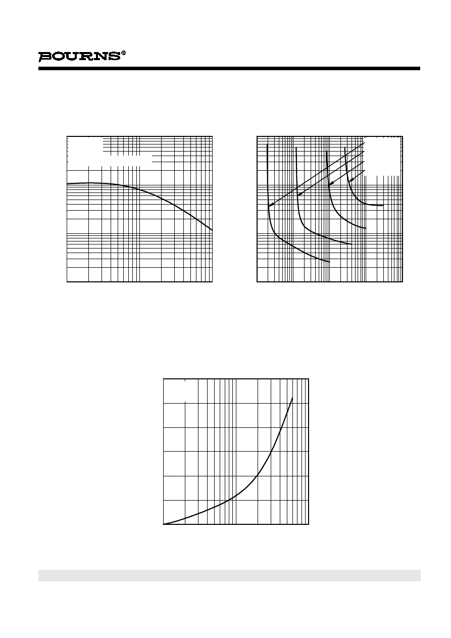
TYPICAL CHARACTERISTICS
Figure 1.
Figure 2.
Figure 3.
TYPICAL DC CURRENT GAIN
vs
COLLECTOR CURRENT
I
C
- Collector Current - A
0·1
1·0
10
h
FE
-
D
C
C
u
rre
n
t
Ga
in
1·0
10
100
1000
TCS633AH
V
CE
= 4 V
T
C
= 25°C
t
p
= 300 µs, duty cycle < 2%
COLLECTOR-EMITTER SATURATION VOLTAGE
vs
BASE CURRENT
I
B
- Base Current - A
0·001
0·01
0·1
1·0
10
V
CE
(s
a
t)
- Co
ll
e
c
to
r-Em
itte
r Sa
tu
ra
ti
o
n
V
o
lt
a
g
e
- V
0·01
0·1
1·0
10
TCS633AE
I
C
= 300 mA
I
C
= 1 A
I
C
= 3 A
I
C
= 6 A
BASE-EMITTER VOLTAGE
vs
COLLECTOR CURRENT
I
C
- Collector Current - A
0·1
1·0
10
V
BE
- Ba
s
e
-E
m
itte
r Vo
lt
a
g
e
- V
0·6
0·7
0·8
0·9
1·0
1·1
1·2
TCS633AF
V
CE
= 4 V
T
C
= 25°C
BD243, BD243A, BD243B, BD243C
NPN SILICON POWER TRANSISTORS
4
JUNE 1973 - REVISED SEPTEMBER 2002
Specifications are subject to change without notice.
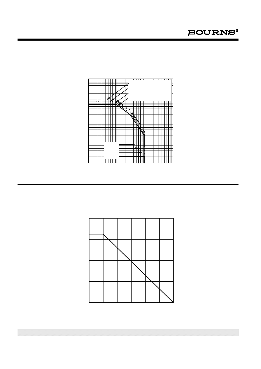
MAXIMUM SAFE OPERATING REGIONS
Figure 4.
THERMAL INFORMATION
Figure 5.
MAXIMUM FORWARD-BIAS
SAFE OPERATING AREA
V
CE
- Collector-Emitter Voltage - V
1·0
10
100
1000
I
C
- Co
ll
e
c
to
r Cu
rre
n
t - A
0·01
0·1
1·0
10
100
SAS633AD
BD243
BD243A
BD243B
BD243C
t
p
= 300 µs, d = 0.1 = 10%
t
p
= 1 ms, d = 0.1 = 10%
t
p
= 10 ms, d = 0.1 = 10%
DC Operation
MAXIMUM POWER DISSIPATION
vs
CASE TEMPERATURE
T
C
- Case Temperature - °C
0
25
50
75
100
125
150
P
to
t
-
Ma
xi
mu
m
P
o
w
e
r D
is
s
ip
at
io
n
-
W
0
10
20
30
40
50
60
70
80
TIS633AB
BD243, BD243A, BD243B, BD243C
NPN SILICON POWER TRANSISTORS
5
JUNE 1973 - REVISED SEPTEMBER 2002
Specifications are subject to change without notice.
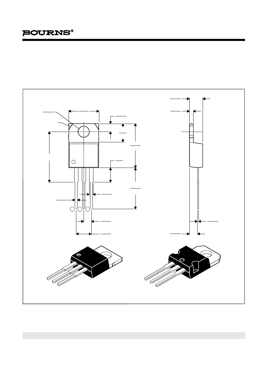
TO-220
3-pin plastic flange-mount package
This single-in-line package consists of a circuit mounted on a lead frame and encapsulated within a plastic
compound. The compound will withstand soldering temperature with no deformation, and circuit performance
characteristics will remain stable when operated in high humidity conditions. Leads require no additional
cleaning or processing when used in soldered assembly.
MECHANICAL DATA
TO220
ALL LINEAR DIMENSIONS IN MILLIMETERS
ø
1,23
1,32
4,20
4,70
1
2
3
0,97
0,61
see Note C
see Note B
10,0
10,4
2,54
2,95
6,0
6,6
14,55
15,90
12,7
14,1
3,5
6,1
1,07
1,70
2,34
2,74
4,88
5,28
3,71
3,96
0,41
0,64
2,40
2,90
VERSION 2
VERSION 1
NOTES: A. The centre pin is in electrical contact with the mounting tab.
B. Mounting tab corner profile according to package version.
C. Typical fixing hole centre stand off height according to package version.
Version
1,
18.0
mm.
Version
2,
17.6
mm.
MDXXBE
Wyszukiwarka
Podobne podstrony:
więcej podobnych podstron