
Chapter 5
Feedback and Stability Theory
Literature Number SLOA077
Excerpted from
Op Amps for Everyone
Literature Number: SLOD006A

5-1
Feedback and Stability Theory
Ron Mancini
5.1
Why Study Feedback Theory?
The gain of all op amps decreases as frequency increases, and the decreasing gain re-
sults in decreasing accuracy as the ideal op amp assumption (a
⇒ ∝
) breaks down. In
most real op amps the open loop gain starts to decrease before 10 Hz, so an understand-
ing of feedback is required to predict the closed loop performance of the op amp. The real
world application of op amps is feedback controlled, and depends on op amp open loop
gain at a given frequency. A designer must know theory to be able to predict the circuit
response regardless of frequency or open loop gain.
Analysis tools have something in common with medicine because they both can be dis-
tasteful but necessary. Medicine often tastes bad or has undesirable side effects, and
analysis tools involve lots of hard learning work before they can be applied to yield results.
Medicine assists the body in fighting an illness; analysis tools assist the brain in learning/
designing feedback circuits.
The analysis tools given here are a synopsis of salient points; thus they are detailed
enough to get you where you are going without any extras. The references, along with
thousands of their counterparts, must be consulted when making an in-depth study of the
field. Aspirin, home remedies, and good health practice handle the majority of health prob-
lems, and these analysis tools solve the majority of circuit problems.
Ideal op amp circuits can be designed without knowledge of feedback analysis tools, but
these circuits are limited to low frequencies. Also, an understanding of feedback analysis
tools is required to understand AC effects like ringing and oscillations.
5.2
Block Diagram Math and Manipulations
Electronic systems and circuits are often represented by block diagrams, and block dia-
grams have a unique algebra and set of transformations[1]. Block diagrams are used be-
cause they are a shorthand pictorial representation of the cause-and-effect relationship
between the input and output in a real system. They are a convenient method for charac-
terizing the functional relationships between components. It is not necessary to under-
stand the functional details of a block to manipulate a block diagram.
Chapter 5
Block Diagram Math and Manipulations
5-2
The input impedance of each block is assumed to be infinite to preclude loading. Also,
the output impedance of each block is assumed to be zero to enable high fan-out. The
systems designer sets the actual impedance levels, but the fan-out assumption is valid
because the block designers adhere to the system designer’s specifications. All blocks
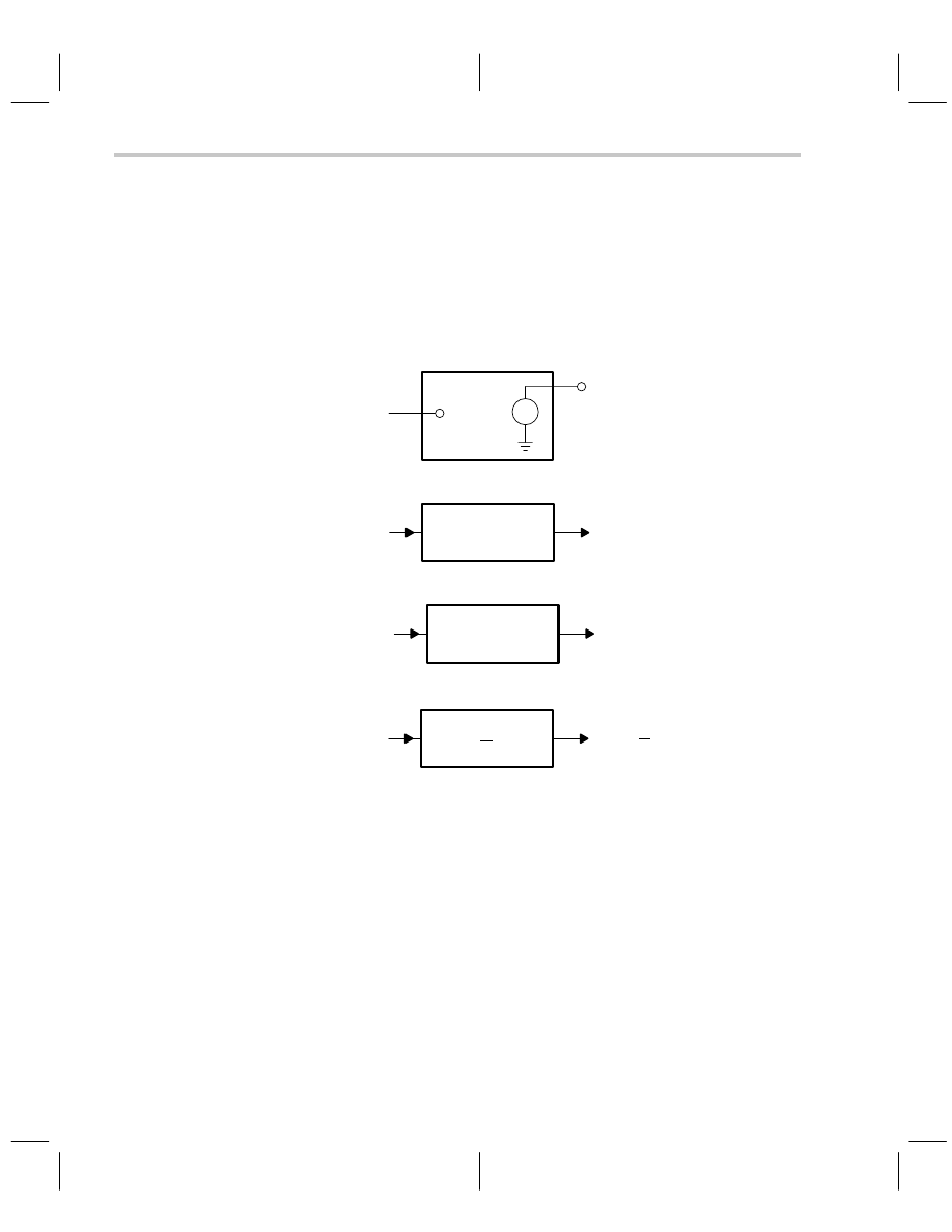
multiply the input times the block quantity (see Figure 5–1) unless otherwise specified
within the block. The quantity within the block can be a constant as shown in Figure
5–1(c), or it can be a complex math function involving Laplace transforms. The blocks can
perform time-based operations such as differentiation and integration.
VO
INPUT
OUTPUT
(a) Input/Output Impedance
A
Block
Description
B
(b) Signal Flow Arrows
A
K
B
B = AK
(c) Block Multiplication
VI
d
dt
VO =
dVI
dt
(d) Blocks Perform Functions as Indicated
Figure 5–1. Definition of Blocks
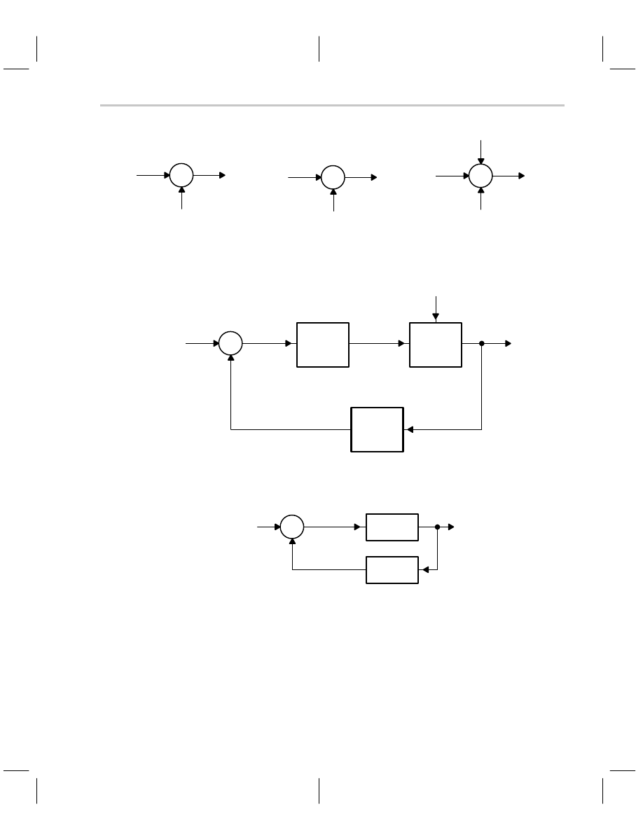
Adding and subtracting are done in special blocks called summing points. Figure 5–2
gives several examples of summing points. Summing points can have unlimited inputs,
can add or subtract, and can have mixed signs yielding addition and subtraction within
a single summing point. Figure 5–3 defines the terms in a typical control system, and Fig-
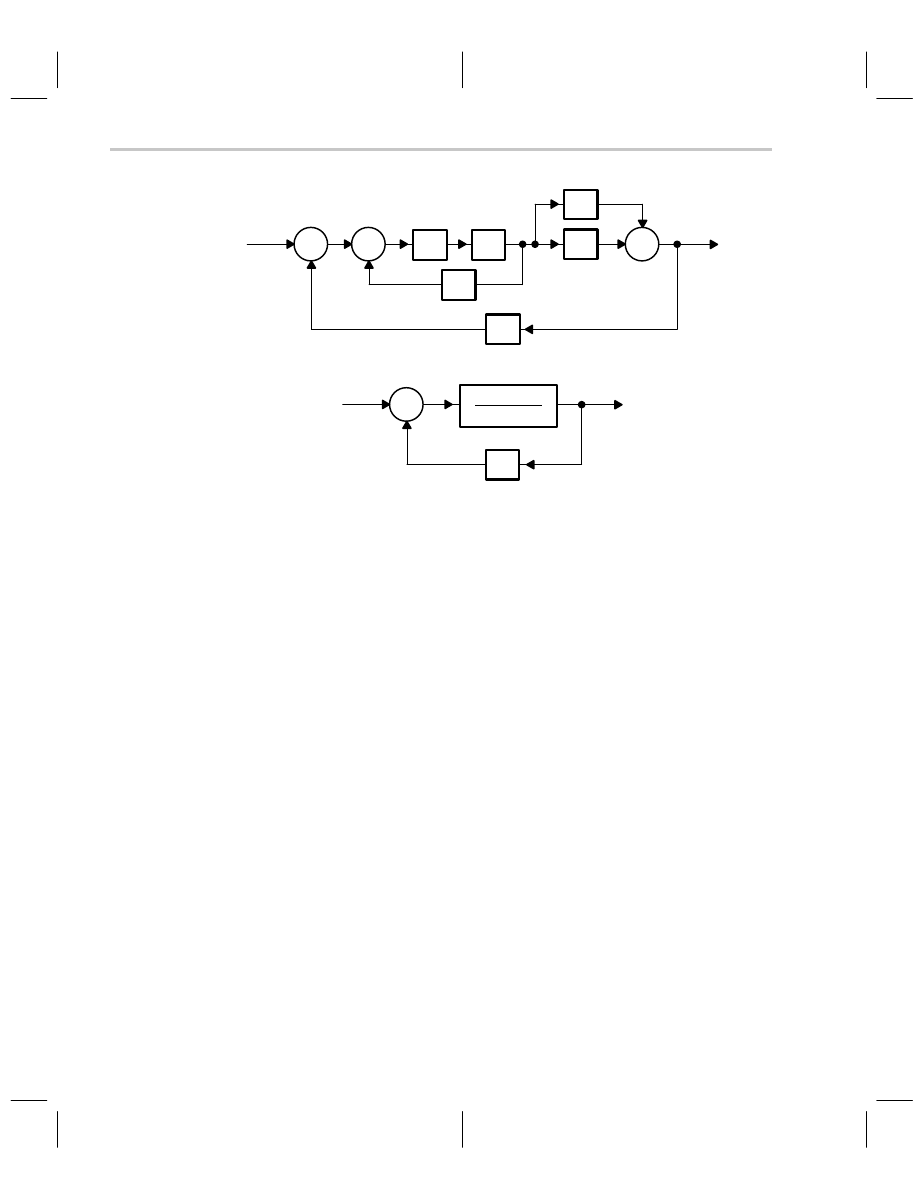
ure 5–4 defines the terms in a typical electronic feedback system. Multiloop feedback sys-
tems (Figure 5–5) are intimidating, but they can be reduced to a single loop feedback sys-
tem, as shown in the figure, by writing equations and solving for V
OUT
/V
IN
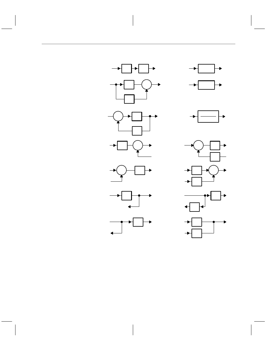
. An easier meth-
od for reducing multiloop feedback systems to single loop feedback systems is to follow
the rules and use the transforms given in Figure 5–6.
Block Diagram Math and Manipulations
5-3
Feedback and Stability Theory
(a) Additive Summary Point
(b) Subtractive Summary Point
(c) Multiple Input Summary Points
+
+
A
A+B
B
+
–
A
A–B
B
+
+
A
A+B–C
B
–
C
Figure 5–2. Summary Points
+
±
R
E = R
±
B
B
Reference
Input
Actuating
Signal
Control
Elements
G1
Manipulated
Variable
M
Plant
G1
U
Disturbance
Controlled
Output
C
Feedback
Elements
H
Forward Path
Feedback Path
Primary
Feedback
Signal
Σ
Figure 5–3. Definition of Control System Terms
E
VIN
A
Σ
β
VOUT
ERROR
Figure 5–4. Definition of an Electronic Feedback Circuit
Block Diagram Math and Manipulations
5-4
+
R
G1
C
–
+
+
G4
H1
G3
G2
+
H2
+
+
R
–
H2
G1G4(G2 + G3)
1 – G1G4H1
C
Figure 5–5. Multiloop Feedback System
Block diagram reduction rules:
D
Combine cascade blocks.
D
Combine parallel blocks.
D
Eliminate interior feedback loops.
D
Shift summing points to the left.
D
Shift takeoff points to the right.
D
Repeat until canonical form is obtained.
Figure 5–6 gives the block diagram transforms. The idea is to reduce the diagram to its
canonical form because the canonical feedback loop is the simplest form of a feedback
loop, and its analysis is well documented. All feedback systems can be reduced to the
canonical form, so all feedback systems can be analyzed with the same math. A canonical
loop exists for each input to a feedback system; although the stability dynamics are inde-
pendent of the input, the output results are input dependent. The response of each input
of a multiple input feedback system can be analyzed separately and added through super-
position.
Block Diagram Math and Manipulations
5-5
Feedback and Stability Theory
K1
K2
K2
A
B
Transformation
Before Transformation
After Transformation
K1
Σ
+
±
B
A
Combine Cascade
Blocks
Combine Parallel
Blocks
K1 K2
A
B
K1
±
K2
A
B
K2
K1
B
A
Eliminate a
Feedback Loop
K1
1
±
K1 K2
A
B
Σ
+
±
K
Σ
+
±
C
A
Move Summer
In Front of a Block
B
K
Σ
+
±
C
A
B
1/K
K
Σ
+
±
C
A
Move Summer
Behind a Block
B
K
Σ
+
±
C
A
B
K
K
B
A
Move Pickoff In
Front of a Block
B
K
B
A
B
K
K
B
A
Move Pickoff
Behind a Block
A
K
B
A
A
I/K
Figure 5–6. Block Diagram Transforms
Feedback Equation and Stability
5-6
5.3
Feedback Equation and Stability
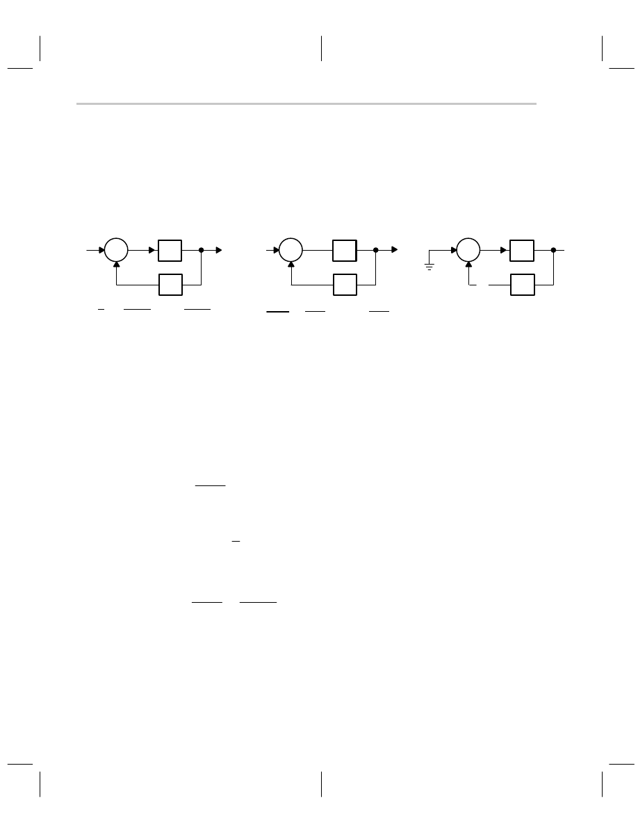
Figure 5–7 shows the canonical form of a feedback loop with control system and electron-
ic system terms. The terms make no difference except that they have meaning to the sys-
tem engineers, but the math does have meaning, and it is identical for both types of terms.
The electronic terms and negative feedback sign are used in this analysis, because sub-
sequent chapters deal with electronic applications. The output equation is written in Equa-
tion 5–1.
H
G
C
R
Σ
+
–
E
C
R
=
G
1 + GH
E =
R
1 + GH
(a) Control System Terminology
(b) Electronics Terminology
(c) Feedback Loop is Broken to
Calculate the Loop Gain
β
A
VOUT
VIN
Σ
+
–
E
VOUT
VIN
=
A
1 + A
β
E =
VIN
1 + A
β
β
A
Σ
+
E
–
X
Figure 5–7. Comparison of Control and Electronic Canonical Feedback Systems
(5–1)
V
OUT
+
EA
The error equation is written in Equation 5–2.
(5–2)
E
+
V
IN
* b
V
OUT
Combining Equations 5–1 and 5–2 yields Equation 5–3.
(5–3)
V
OUT
A
+
V
IN
* b
V
OUT
Collecting terms yields Equation 5–4.
(5–4)
V
OUT
ǒ
1
A
) b
Ǔ
+
V
IN
Rearranging terms yields the classic form of the feedback Equation 5–5.
(5–5)
V
OUT
V
IN
+
A
1
)
A
b
When the quantity A
β
in Equation 5–5 becomes very large with respect to one, the one
can be neglected, and Equation 5–5 reduces to Equation 5–6, which is the ideal feedback
equation. Under the conditions that A
β
>>1, the system gain is determined by the feed-
back factor
β
. Stable passive circuit components are used to implement the feedback fac-
tor, thus in the ideal situation, the closed loop gain is predictable and stable because
β
is predictable and stable.

Bode Analysis of Feedback Circuits
5-7
Feedback and Stability Theory
(5–6)
V
OUT
V
IN
+
1
b
The quantity A
β
is so important that it has been given a special name: loop gain. In Figure
5–7, when the voltage inputs are grounded (current inputs are opened) and the loop is
broken, the calculated gain is the loop gain, A
β
. Now, keep in mind that we are using com-
plex numbers, which have magnitude and direction. When the loop gain approaches mi-
nus one, or to express it mathematically 1
∠
–180
°
, Equation 5–5 approaches 1/0
⇒
∝
.
The circuit output heads for infinity as fast as it can using the equation of a straight line.
If the output were not energy limited, the circuit would explode the world, but happily, it
is energy limited, so somewhere it comes up against the limit.
Active devices in electronic circuits exhibit nonlinear phenomena when their output ap-
proaches a power supply rail, and the nonlinearity reduces the gain to the point where the
loop gain no longer equals 1
∠
–180
°
. Now the circuit can do two things: first it can become
stable at the power supply limit, or second, it can reverse direction (because stored
charge keeps the output voltage changing) and head for the negative power supply rail.
The first state where the circuit becomes stable at a power supply limit is named lockup;
the circuit will remain in the locked up state until power is removed and reapplied. The
second state where the circuit bounces between power supply limits is named oscillatory.
Remember, the loop gain, A
β
, is the sole factor determining stability of the circuit or sys-
tem. Inputs are grounded or disconnected, so they have no bearing on stability.
Equations 5–1 and 5–2 are combined and rearranged to yield Equation 5–7, which is the
system or circuit error equation.
(5–7)
E
+
V
IN
1
)
A
b
First, notice that the error is proportional to the input signal. This is the expected result
because a bigger input signal results in a bigger output signal, and bigger output signals
require more drive voltage. As the loop gain increases, the error decreases, thus large
loop gains are attractive for minimizing errors.
5.4
Bode Analysis of Feedback Circuits
H. W. Bode developed a quick, accurate, and easy method of analyzing feedback amplifi-
ers, and he published a book about his techniques in 1945.[2] Operational amplifiers had
not been developed when Bode published his book, but they fall under the general classi-
fication of feedback amplifiers, so they are easily analyzed with Bode techniques. The
mathematical manipulations required to analyze a feedback circuit are complicated be-
cause they involve multiplication and division. Bode developed the Bode plot, which sim-
plifies the analysis through the use of graphical techniques.
Bode Analysis of Feedback Circuits
5-8
The Bode equations are log equations that take the form 20LOG(F(t)) = 20LOG(|F(t)|) +
phase angle. Terms that are normally multiplied and divided can now be added and sub-
tracted because they are log equations. The addition and subtraction is done graphically,
thus easing the calculations and giving the designer a pictorial representation of circuit
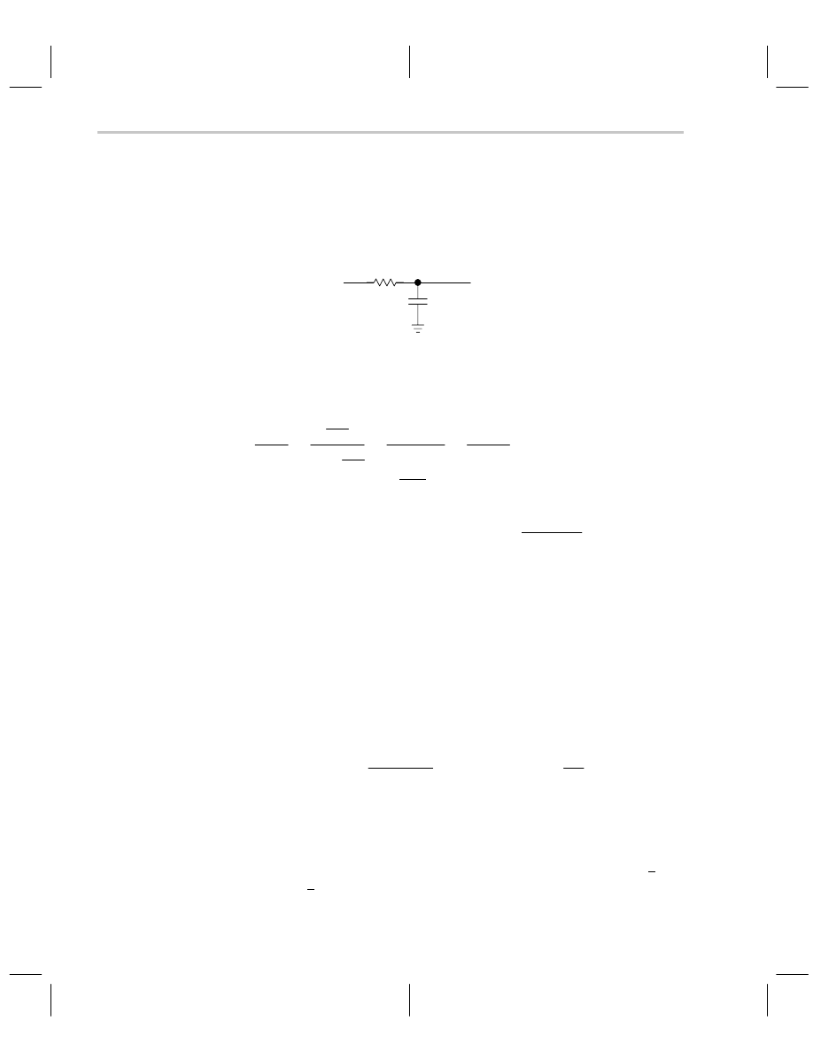
performance. Equation 5–8 is written for the low pass filter shown in Figure 5–8.
VI
VO
R
C
Figure 5–8. Low-Pass Filter
(5–8)
V
OUT
V
IN
+
1
C s
R
)
1
C s
+
1
1
)
RCs
+
1
1
) t
s
Where: s = j
ω
, j =
√
(–1), and RC =
τ
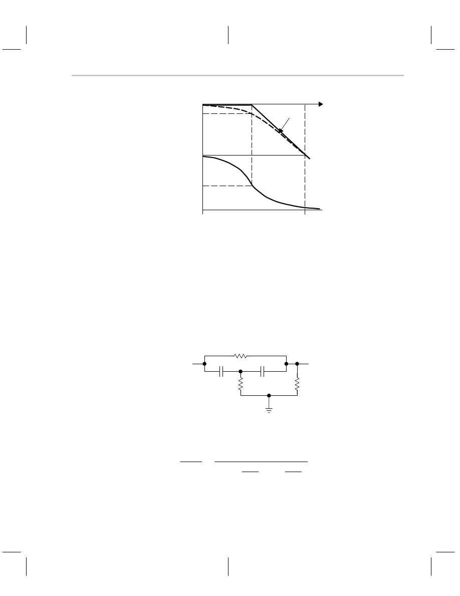
The magnitude of this transfer function is
|
V
OUT
ń
V
IN
|
+
1
ń
1
2
)
(
tw
)
2
Ǹ
. This magnitude,
|V
OUT
/V
IN
|
≅
1 when
ω
= 0.1/
τ
, it equals 0.707 when
ω
= 1/
τ
, and it is approximately = 0.1
when
ω
= 10/
τ
.
These points are plotted in Figure 5–9 using straight line approximations.
The negative slope is –20 dB/decade or –6 dB/octave. The magnitude curve is plotted as
a horizontal line until it intersects the breakpoint where
ω
= 1/
τ
. The negative slope begins
at the breakpoint because the magnitude starts decreasing at that point. The gain is equal
to 1 or 0 dB at very low frequencies, equal to 0.707 or –3 dB at the break frequency, and
it keeps falling with a –20 dB/decade slope for higher frequencies.
The phase shift for the low pass filter or any other transfer function is calculated with the
aid of Equation 5–9.
(5–9)
f +
tangent
*
1
ǒ
Real
Imaginary
Ǔ
+ *
tangent
*
1
ǒ
wt
1
Ǔ
The phase shift is much harder to approximate because the tangent function is nonlinear.
Normally the phase information is only required around the 0 dB intercept point for an ac-
tive circuit, so the calculations are minimized. The phase is shown in Figure 5–9, and it
is approximated by remembering that the tangent of 90
°
is 1, the tangent of 60
°
is
√
3 , and
the tangent of 30
°
is
√
3/3.
Bode Analysis of Feedback Circuits
5-9
Feedback and Stability Theory
ω
= 0.1/
τ
ω
= 1/
τ
ω
= 10/
τ
0 dB
–3 dB
–20 dB
0
°
–45
°
–90
°
Phase Shift
–20 dB/Decade
20 Log (V
O
/V
I)
Figure 5–9. Bode Plot of Low-Pass Filter Transfer Function
A breakpoint occurring in the denominator is called a pole, and it slopes down. Converse-
ly, a breakpoint occurring in the numerator is called a zero, and it slopes up. When the
transfer function has multiple poles and zeros, each pole or zero is plotted independently,
and the individual poles/zeros are added graphically. If multiple poles, zeros, or a pole/
zero combination have the same breakpoint, they are plotted on top of each other. Multiple
poles or zeros cause the slope to change by multiples of 20 dB/decade.
An example of a transfer function with multiple poles and zeros is a band reject filter (see
Figure 5–10). The transfer function of the band reject filter is given in Equation 5–10.
R
C
C
R
R
VOUT
VIN
RC =
τ
Figure 5–10. Band Reject Filter
(5–10)
G
+
V
OUT
V
IN
+
(1
) t
s)(1
) t
s)
2
ǒ
1
) t
s
0.44
Ǔ ǒ
1
) t
s
4.56
Ǔ
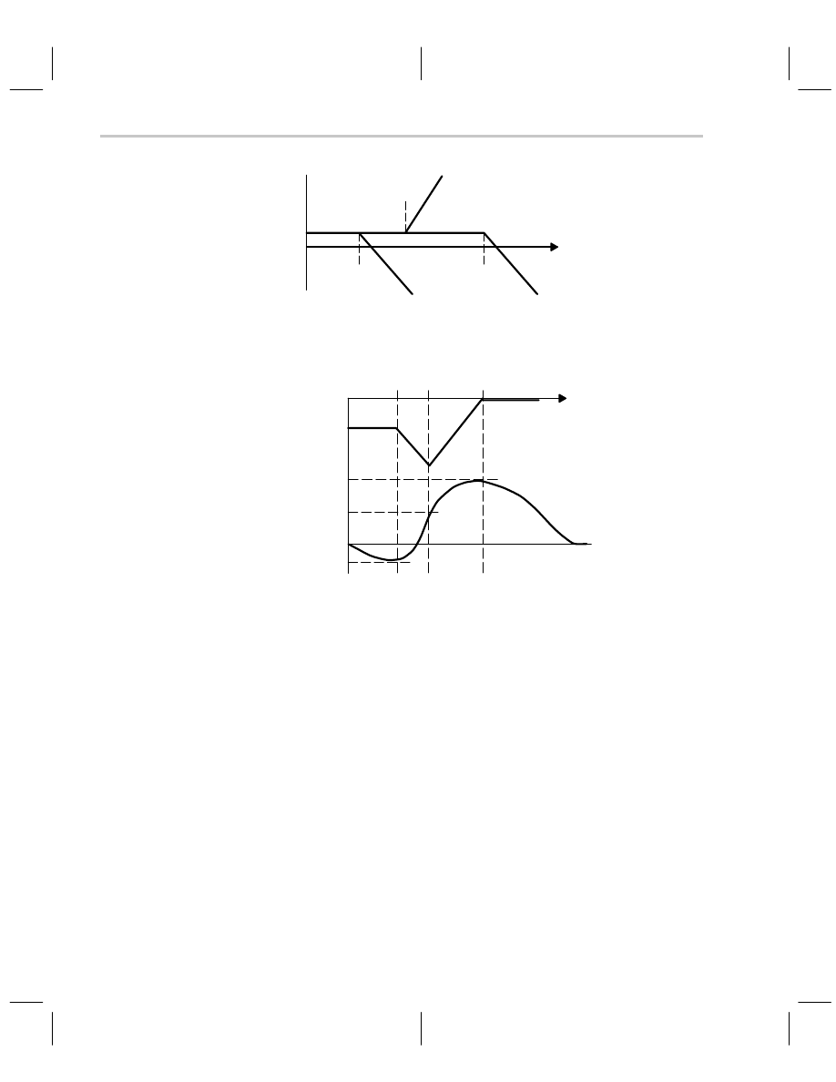
The pole zero plot for each individual pole and zero is shown in Figure 5–11, and the com-
bined pole zero plot is shown in Figure 5–12.
Bode Analysis of Feedback Circuits
5-10
ω
= 1/
τ
40 dB/Decade
LOG (
ω
)
–20 dB/Decade
ω
= 4.56/
τ
ω
= 0.44/
τ
–20 dB/Decade
dB
0
–6
Amplitude
Figure 5–11.Individual Pole Zero Plot of Band Reject Filter
0 dB
–6 dB
12
°
0
Phase Shift
LOG (
ω
)
ω
= 1/
τ
ω
= 0.44/
τ
ω
= 4.56/
τ
25
°
–5
°
Amplitude
Figure 5–12. Combined Pole Zero Plot of Band Reject Filter
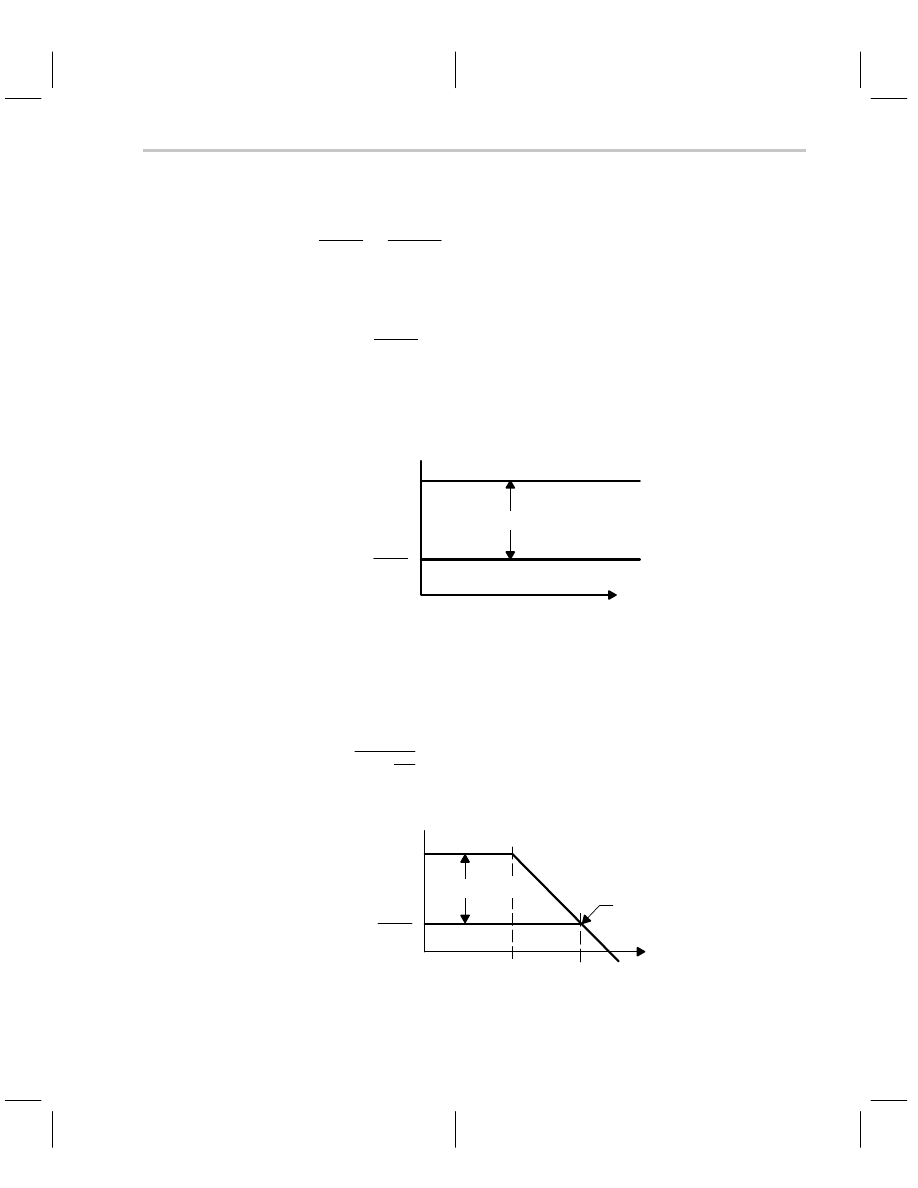
The individual pole zero plots show the dc gain of 1/2 plotting as a straight line from the
–6 dB intercept. The two zeros occur at the same break frequency, thus they add to a
40-dB/decade slope. The two poles are plotted at their breakpoints of
ω
= 0.44/
τ
and
ω
= 4.56/
τ
. The combined amplitude plot intercepts the amplitude axis at –6 dB because
of the dc gain, and then breaks down at the first pole. When the amplitude function gets
to the double zero, the first zero cancels out the first pole, and the second zero breaks
up. The upward slope continues until the second pole cancels out the second zero, and
the amplitude is flat from that point out in frequency.
When the separation between all the poles and zeros is great, a decade or more in fre-
quency, it is easy to draw the Bode plot. As the poles and zeros get closer together, the
plot gets harder to make. The phase is especially hard to plot because of the tangent func-
tion, but picking a few salient points and sketching them in first gets a pretty good approxi-
mation.[3] The Bode plot enables the designer to get a good idea of pole zero placement,
and it is valuable for fast evaluation of possible compensation techniques. When the situa-
tion gets critical, accurate calculations must be made and plotted to get an accurate result.
Bode Analysis of Feedback Circuits
5-11
Feedback and Stability Theory
Consider Equation 5–11.
(5–11)
V
OUT
V
IN
+
A
1
)
A
b
Taking the log of Equation 5–11 yields Equation 5–12.
(5–12)
20Log
ǒ
V
OUT
V
IN
Ǔ
+
20Log(A)–20Log(1
)
A
b
)
If A and
β
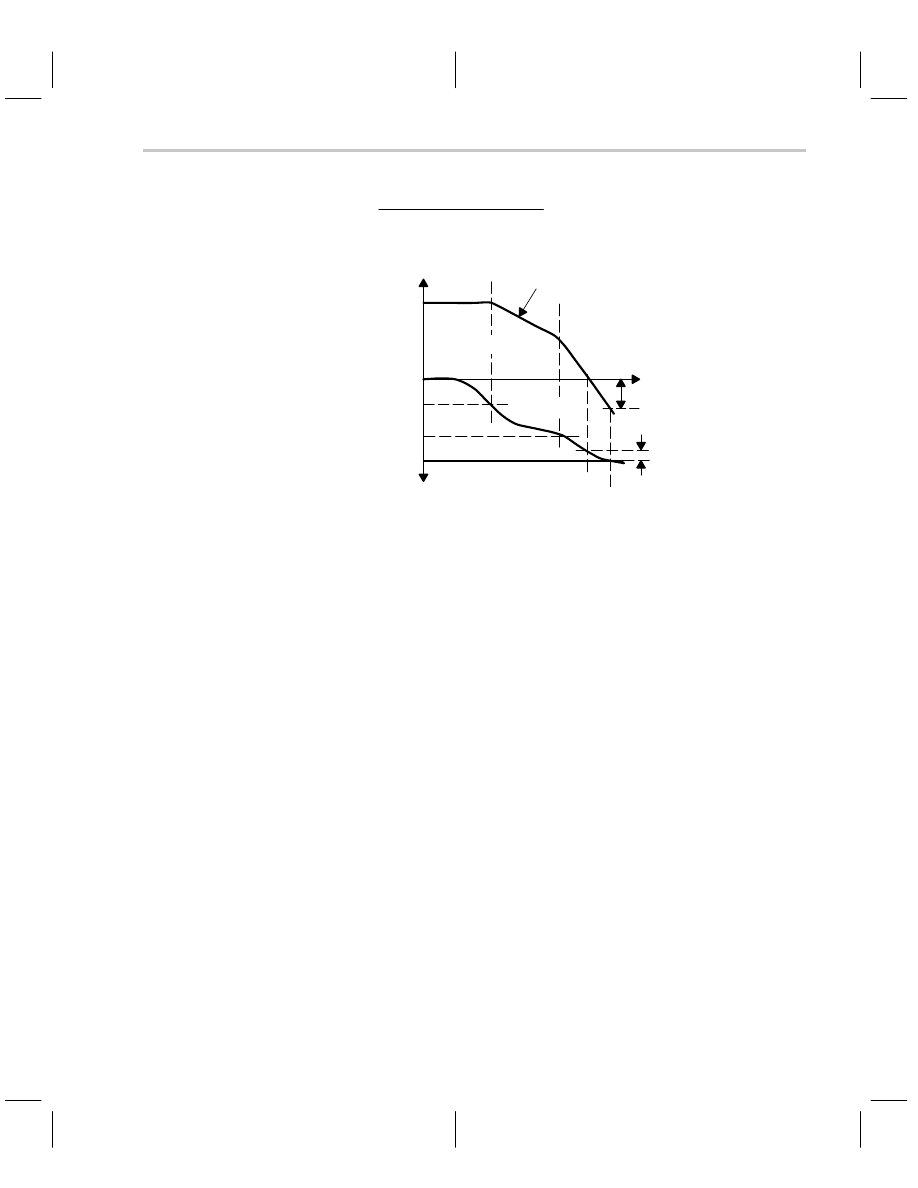
do not contain any poles or zeros there will be no break points. Then the Bode
plot of Equation 5–12 looks like that shown in Figure 5–13, and because there are no
poles to contribute negative phase shift, the circuit cannot oscillate.
20 LOG(1 + A
β
)
dB
20 LOG(A)
0 dB
LOG(
ω
)
Amplitude 20 LOG
ǒ
V
OUT
V
IN
Ǔ
Figure 5–13. When No Pole Exists in Equation (5–12)
All real amplifiers have many poles, but they are normally internally compensated so that
they appear to have a single pole. Such an amplifier would have an equation similar to
that given in Equation 5–13.
(5–13)
A
+
a
1
)
j
w
w
a
The plot for the single pole amplifier is shown in Figure 5–14.
ω
=
ω
a
ω
dB
0 dB
20 LOG(1 + A
β
)
LOG(
ω
)
Amplitude
20 LOG(A)
x
20 LOG
ǒ
V
OUT
V
IN
Ǔ
Figure 5–14. When Equation 5–12 has a Single Pole

Loop Gain Plots are the Key to Understanding Stability
5-12
The amplifier gain, A, intercepts the amplitude axis at 20Log(A), and it breaks down at a
slope of –20 dB/decade at
ω
=
ω
a
. The negative slope continues for all frequencies greater
than the breakpoint,
ω
=
ω
a
. The closed loop circuit gain intercepts the amplitude axis at
20Log(V
OUT
/V
IN
), and because
β
does not have any poles or zeros, it is constant until its
projection intersects the amplifier gain at point X. After intersection with the amplifier gain
curve, the closed loop gain follows the amplifier gain because the amplifier is the control-
ling factor.
Actually, the closed loop gain starts to roll off earlier, and it is down 3 dB at point X. At point
X the difference between the closed loop gain and the amplifier gain is –3 dB, thus accord-
ing to Equation 5–12 the term –20Log(1+A
β
) = –3 dB. The magnitude of 3 dB is
√
2 , hence
1
)
(A
b
)
2
Ǹ
+
2
Ǹ
, and elimination of the radicals shows that A
β
= 1. There is a method
[4] of relating phase shift and stability to the slope of the closed loop gain curves, but only
the Bode method is covered here. An excellent discussion of poles, zeros, and their inter-
action is given by M. E Van Valkenberg,[5] and he also includes some excellent prose to
liven the discussion.
5.5
Loop Gain Plots are the Key to Understanding Stability
Stability is determined by the loop gain, and when A
β
= –1 = |1|
∠
–180
°
instability or os-
cillation occurs. If the magnitude of the gain exceeds one, it is usually reduced to one by
circuit nonlinearities, so oscillation generally results for situations where the gain magni-
tude exceeds one.
Consider oscillator design, which depends on nonlinearities to decrease the gain magni-
tude; if the engineer designed for a gain magnitude of one at nominal circuit conditions,
the gain magnitude would fall below one under worst case circuit conditions causing os-
cillation to cease. Thus, the prudent engineer designs for a gain magnitude of one under
worst case conditions knowing that the gain magnitude is much more than one under opti-
mistic conditions. The prudent engineer depends on circuit nonlinearities to reduce the
gain magnitude to the appropriate value, but this same engineer pays a price of poorer
distortion performance. Sometimes a design compromise is reached by putting a nonlin-
ear component, such as a lamp, in the feedback loop to control the gain without introduc-
ing distortion.
Some high gain control systems always have a gain magnitude greater than one, but they
avoid oscillation by manipulating the phase shift. The amplifier designer who pushes the
amplifier for superior frequency performance has to be careful not to let the loop gain
phase shift accumulate to 180
°
. Problems with overshoot and ringing pop up before the
loop gain reaches 180
°
phase shift, thus the amplifier designer must keep a close eye on
loop dynamics. Ringing and overshoot are handled in the next section, so preventing os-
cillation is emphasized in this section. Equation 5–14 has the form of many loop gain
transfer functions or circuits, so it is analyzed in detail.
Loop Gain Plots are the Key to Understanding Stability
5-13
Feedback and Stability Theory
(5–14)
(A)
b +
(K)
ǒ
1
) t
1
(s)
Ǔǒ
1
) t
2
(s)
Ǔ
dB
20 LOG(K)
0 dB
–45
–135
–180
LOG(f)
Phase (A
β
)
Amplitude (A
β
)
20 LOG(A
β
)
GM
φ
M
1/
τ
1
1/
τ
2
Figure 5–15. Magnitude and Phase Plot of Equation 5–14
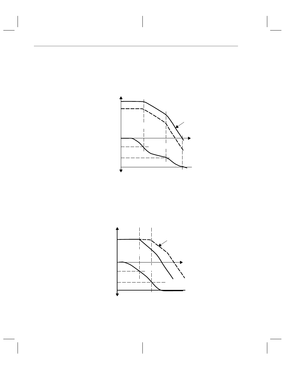
The quantity, K, is the dc gain, and it plots as a straight line with an intercept of 20Log(K).
The Bode plot of Equation 5–14 is shown in Figure 5–15. The two break points,
ω
=
ω
1
= 1/
τ
1
and
ω
=
ω
2
= 1/
τ
2
, are plotted in the Bode plot. Each breakpoint adds –20 dB/decade
slope to the plot, and 45
°
phase shift accumulates at each breakpoint. This transfer func-
tion is referred to as a two slope because of the two breakpoints. The slope of the curve
when it crosses the 0 dB intercept indicates phase shift and the ability to oscillate. Notice
that a one slope can only accumulate 90
°
phase shift, so when a transfer function passes
through 0 dB with a one slope, it cannot oscillate. Furthermore, a two-slope system can
accumulate 180
°
phase shift, therefore a transfer function with a two or greater slope is
capable of oscillation.
A one slope crossing the 0 dB intercept is stable, whereas a two or greater slope crossing
the 0 dB intercept may be stable or unstable depending upon the accumulated phase
shift. Figure 5–15 defines two stability terms; the phase margin,
φ
M
, and the gain margin,
G
M
. Of these two terms the phase margin is much more important because phase shift
is critical for stability. Phase margin is a measure of the difference in the actual phase shift
and the theoretical 180
°
required for oscillation, and the phase margin measurement or
calculation is made at the 0 dB crossover point. The gain margin is measured or calcu-
lated at the 180
°
phase crossover point. Phase margin is expressed mathematically in
Equation 5–15.
(5–15)
f
M
+
180
*
tangent
–1
(A
b
)
Loop Gain Plots are the Key to Understanding Stability
5-14
The phase margin in Figure 5–15 is very small, 20
°
, so it is hard to measure or predict from
the Bode plot. A designer probably doesn’t want a 20
°
phase margin because the system
overshoots and rings badly, but this case points out the need to calculate small phase mar-
gins carefully. The circuit is stable, and it does not oscillate because the phase margin is
positive. Also, the circuit with the smallest phase margin has the highest frequency re-
sponse and bandwidth.
20 LOG(K + C)
0 dB
–45
–135
–180
LOG(f)
Phase (A
β
)
Amplitude (A
β
)
20 LOG(A
β
)
φ
M = 0
20 LOG(K)
1/
τ
1
1/
τ
2
Figure 5–16. Magnitude and Phase Plot of the Loop Gain Increased to (K+C)
Increasing the loop gain to (K+C) as shown in Figure 5–16 shifts the magnitude plot up.
If the pole locations are kept constant, the phase margin reduces to zero as shown, and
the circuit will oscillate. The circuit is not good for much in this condition because produc-
tion tolerances and worst case conditions ensure that the circuit will oscillate when you
want it to amplify, and vice versa.
LOG(f)
Phase (A
β
)
Amplitude (A
β
)
20 LOG(A
β
)
φ
M = 0
0 dB
–45
–135
–180
20 LOG(K)
dB
1/
τ
1
1/
τ
2
Figure 5–17. Magnitude and Phase Plot of the Loop Gain With Pole Spacing Reduced

The Second Order Equation and Ringing/Overshoot Predictions
5-15
Feedback and Stability Theory
The circuit poles are spaced closer in Figure 5–17, and this results in a faster accumula-
tion of phase shift. The phase margin is zero because the loop gain phase shift reaches
180
°
before the magnitude passes through 0 dB. This circuit oscillates, but it is not a very
stable oscillator because the transition to 180
°
phase shift is very slow. Stable oscillators
have a very sharp transition through 180
°
.
When the closed loop gain is increased the feedback factor,
β
, is decreased because
V
OUT
/V
IN
= 1/
β
for the ideal case. This in turn decreases the loop gain, A
β
, thus the stabil-
ity increases. In other words, increasing the closed loop gain makes the circuit more
stable. Stability is not important except to oscillator designers because overshoot and
ringing become intolerable to linear amplifiers long before oscillation occurs. The over-
shoot and ringing situation is investigated next.
5.6
The Second Order Equation and Ringing/Overshoot Predictions
The second order equation is a common approximation used for feedback system analy-
sis because it describes a two-pole circuit, which is the most common approximation
used. All real circuits are more complex than two poles, but except for a small fraction,
they can be represented by a two-pole equivalent. The second order equation is exten-
sively described in electronic and control literature
[
6
]
.
(5–16)
(1
)
A
b
)
+
1
)
K
ǒ
1
) t
1
s
Ǔ ǒ
1
) t
2
s
Ǔ
After algebraic manipulation Equation 5–16 is presented in the form of Equation 5–17.
(5–17)
s
2
)
S
t
1
) t
2
t
1
t
2
)
1
)
K
t
1
t
2
+
0
Equation 5–17 is compared to the second order control Equation 5–18, and the damping
ratio,
ζ
, and natural frequency, w
N
are obtained through like term comparisons.
(5–18)
s
2
)
2
zw
N
s
) w
2
N
Comparing these equations yields formulas for the phase margin and per cent overshoot
as a function of damping ratio.
(5–19)
w
N
+
1
)
K
t
1
t
2
Ǹ
(5–20)
c +
t
1
) t
2
2
w
N
t
1
t
2
When the two poles are well separated, Equation 5–21 is valid.
References
5-16
(5–21)
f
M
+
tangent
*
1
(2
c
)
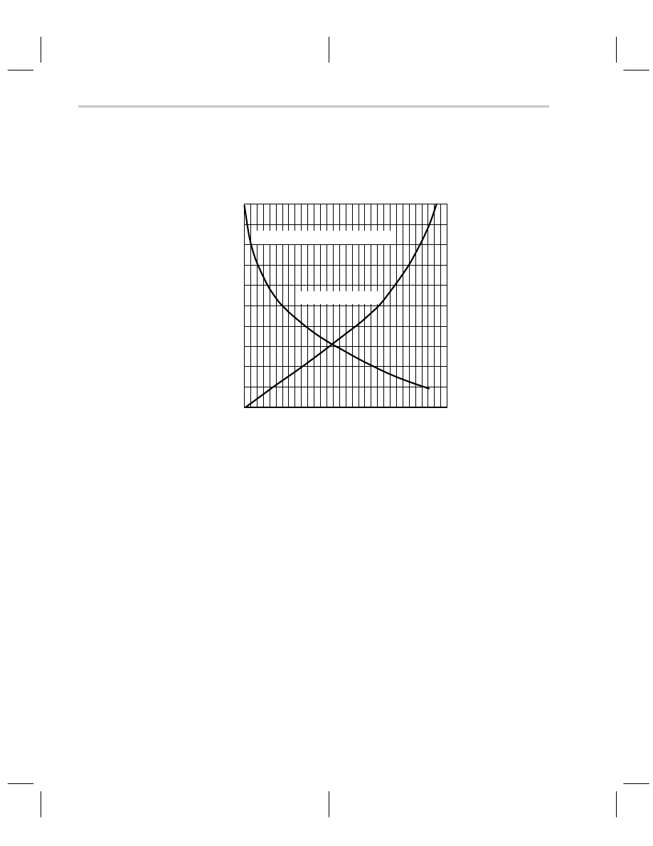
The salient equations are plotted in Figure 5–18, which enables a designer to determine
the phase margin and overshoot when the gain and pole locations are known.
Phase Margin,
φ
M
Percent Maximum Overshoot
0.4
0.2
0
0
10
20
30
40
50
60
Damping Ratio,
0.6
0.8
1
70
80
Figure 5–18. Phase Margin and Overshoot vs Damping Ratio
Enter Figure 5–18 at the calculated damping ratio, say 0.4, and read the overshoot at 25%
and the phase margin at 42
°
. If a designer had a circuit specification of 5% maximum over-
shoot, then the damping ratio must be 0.78 with a phase margin of 62
°
.
5.7
References
1. DiStefano, Stubberud, and Williams, Theory and Problems of
Feedback and Control Systems, Schaum’s Outline Series, Mc
Graw Hill Book Company, 1967
2. Bode, H. W., Network Analysis And Feedback Amplifier Design,
D. Van Nostrand, Inc., 1945
3. Frederickson, Thomas, Intuitive Operational Amplifiers,
McGraw Hill Book Company, 1988
4. Bower, J. L. and Schultheis, P. M., Introduction To The Design Of
Servomechanisms, Wiley, 1961
5. Van Valkenberg, M. E., Network Analysis, Prentice-Hall, 1964
6. Del Toro, V., and Parker, S., Principles of Control Systems
Engineering, McGraw–Hill, 1960.

IMPORTANT NOTICE
Texas Instruments Incorporated and its subsidiaries (TI) reserve the right to make corrections, modifications,
enhancements, improvements, and other changes to its products and services at any time and to discontinue
any product or service without notice. Customers should obtain the latest relevant information before placing
orders and should verify that such information is current and complete. All products are sold subject to TI’s terms
and conditions of sale supplied at the time of order acknowledgment.
TI warrants performance of its hardware products to the specifications applicable at the time of sale in
accordance with TI’s standard warranty. Testing and other quality control techniques are used to the extent TI
deems necessary to support this warranty. Except where mandated by government requirements, testing of all
parameters of each product is not necessarily performed.
TI assumes no liability for applications assistance or customer product design. Customers are responsible for
their products and applications using TI components. To minimize the risks associated with customer products
and applications, customers should provide adequate design and operating safeguards.
TI does not warrant or represent that any license, either express or implied, is granted under any TI patent right,
copyright, mask work right, or other TI intellectual property right relating to any combination, machine, or process
in which TI products or services are used. Information published by TI regarding third–party products or services
does not constitute a license from TI to use such products or services or a warranty or endorsement thereof.
Use of such information may require a license from a third party under the patents or other intellectual property
of the third party, or a license from TI under the patents or other intellectual property of TI.
Reproduction of information in TI data books or data sheets is permissible only if reproduction is without
alteration and is accompanied by all associated warranties, conditions, limitations, and notices. Reproduction
of this information with alteration is an unfair and deceptive business practice. TI is not responsible or liable for
such altered documentation.
Resale of TI products or services with statements different from or beyond the parameters stated by TI for that
product or service voids all express and any implied warranties for the associated TI product or service and
is an unfair and deceptive business practice. TI is not responsible or liable for any such statements.
Mailing Address:
Texas Instruments
Post Office Box 655303
Dallas, Texas 75265
Copyright
2001, Texas Instruments Incorporated
Wyszukiwarka
Podobne podstrony:
Microstructures and stability of retained austenite in TRIP steels
Civil Society and Political Theory in the Work of Luhmann
Marxism and?onomic Theory
Model Loading and stability manual
Glaser Naturalist Inquiry and Grounded Theory
NUCLEAR PHYSICS AND REACTOR THEORY vol2
Prywes Mathematics Of Magic A Study In Probability, Statistics, Strategy And Game Theory Fixed
MERTON Social Problems and Sociological Theory
Fileds and Galois Theory [jnl article] J Milne
NUCLEAR PHYSICS AND REACTOR THEORY vol1
Microstructures and stability of retained austenite in TRIP steels
5 Diversity and Stability in Language
Matlab Tutorial for Systems and Control Theory (MIT) (1999) WW
Einstein A Relativity the special and general theory (free web version, Methuen, 1920) (115s)
Algebra and Number Theory A Baker (2003) WW
Black Holes In Supergravity And String Theory
Narrative Form and Chaos Theory in Sterne, Proust, Woolf, and Faulkner
więcej podobnych podstron