Circuit Operation:
IC1 is an Infra Red module. IR modulated pulses are received and buffered by this IC. It has a standard TTL output, the
output with no signal is logic 1. One gate of a CMOS inverter and drives Red LED1 as a visible switching aid. Another gate
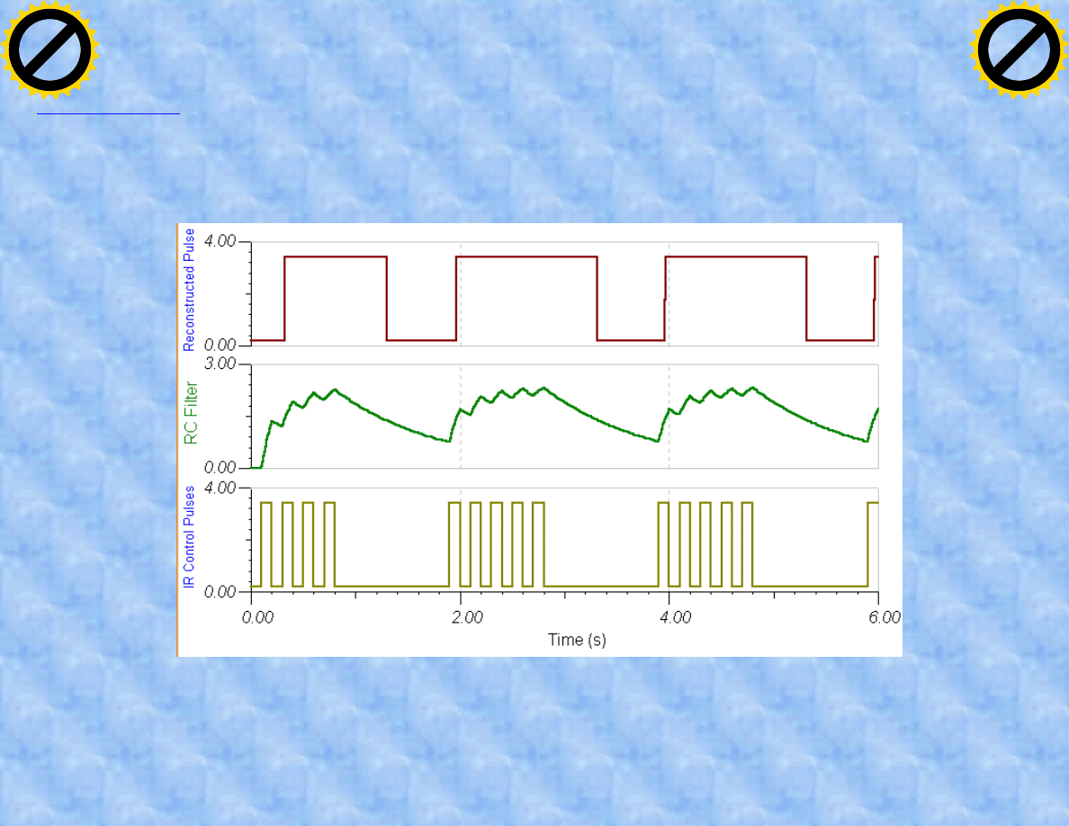
buffers the signal and applies it to the time constant circuit, comprising R3,C2,R4 and D1. C2 charges via R3, and
discharges via R4, D1 prevents quick discharge via the low output impedance of the CMOS buffer.
The pulses are further buffered and contain "jaggered edges" as shown above. These edges are produced by the
modulated IR data, which has to be removed. This is achieved using IC3, a 555 timer wired as a monostable, pulse duration
R5, C4. These cleanly reconstructs a single clean pulse to activate the bistable latch. A D type flip flop, IC4 is configured as
a bistable. The input is applied to the clock pin, the inverted output fed back to the data input and clear and preset lines are
tied to ground. For every pulse the relay will operate and latch, the next pulse will turn off the relay and so on. Note that
Wyszukiwarka
Podobne podstrony:
a lot of various circuits index 9028613 25 4790
a lot of various circuits index 2628613 25 4526
a lot of various circuits index 7528613 25 4775
a lot of various circuits index 8228613 25 4782
a lot of various circuits index 8528613 25 4785
a lot of various circuits index 27628613 25 52276
a lot of various circuits index 25328613 25 51253
a lot of various circuits index 16028613 25 49160
a lot of various circuits index 19228613 25 50192
a lot of various circuits index 2428613 25 4524
a lot of various circuits index 9828613 25 4798
a lot of various circuits index 6328613 25 4663
a lot of various circuits index 17728613 25 49177
a lot of various circuits index 5328613 25 4653
a lot of various circuits index 328613 25 453
a lot of various circuits index 4428613 25 4644
a lot of various circuits index 928613 25 459
a lot of various circuits index 428613 25 454
więcej podobnych podstron