
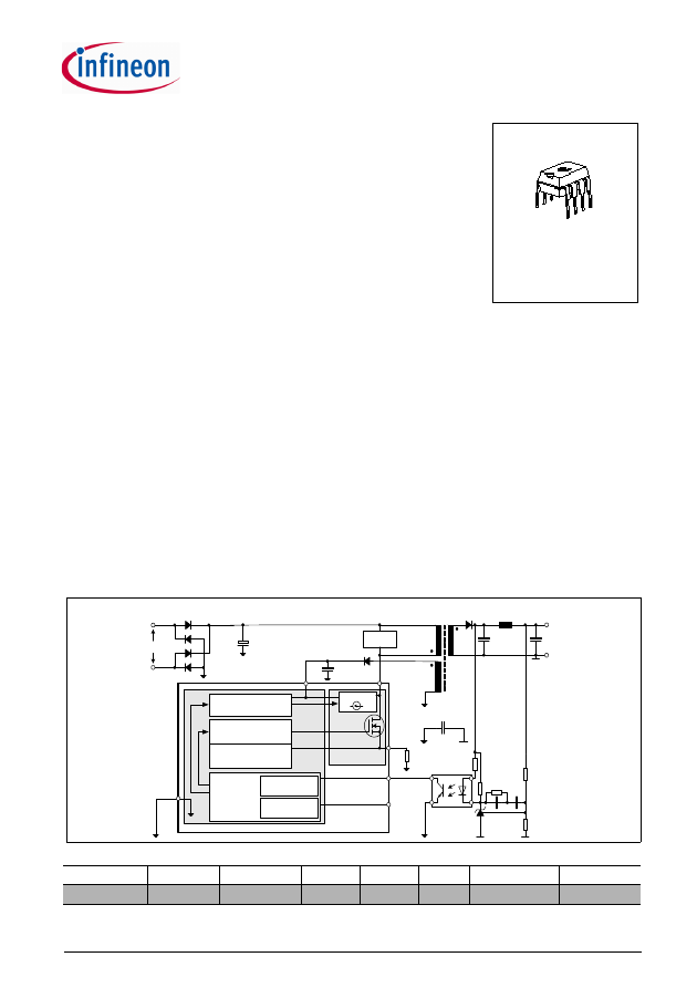
CoolSET
®
-F3R
ICE3BR1765J
Off-Line SMPS Current Mode
Controller with integrated 650V
CoolMOS
®
and Startup cell
(frequency jitter Mode) in DIP-8
N e v e r s t o p t h i n k i n g .
Power Management & Supply
Version 2.3, 19 Nov 2012

Edition 2012-11-19
Published by
Infineon Technologies AG,
81726 Munich, Germany,
©
2012 Infineon Technologies AG.
All Rights Reserved.
Legal disclaimer
The information given in this document shall in no event be regarded as a guarantee of conditions or
characteristics. With respect to any examples or hints given herein, any typical values stated herein and/or any
information regarding the application of the device, Infineon Technologies hereby disclaims any and all warranties
and liabilities of any kind, including without limitation, warranties of non-infringement of intellectual property rights
of any third party.
Information
For further information on technology, delivery terms and conditions and prices, please contact your nearest
Infineon Technologies Office (www.infineon.com).
Warnings
Due to technical requirements, components may contain dangerous substances. For information on the types in
question, please contact your nearest Infineon Technologies Office.
Infineon Technologies Components may be used in life-support devices or systems only with the express written
approval of Infineon Technologies, if a failure of such components can reasonably be expected to cause the failure
of that life-support device or system or to affect the safety or effectiveness of that device or system. Life support
devices or systems are intended to be implanted in the human body or to support and/or maintain and sustain
and/or protect human life. If they fail, it is reasonable to assume that the health of the user or other persons may
be endangered.
For questions on technology, delivery and prices please contact the Infineon Technologies Offices in Germany or
the Infineon Technologies Companies and Representatives worldwide: see our webpage at http://
www.infineon.com
CoolMOS
®
, CoolSET
®
are trademarks of Infineon Technologies AG.
CoolSET
®
-F3R
ICE3BR1765J
Revision History:
2012-11-19
Datasheet
Previous Version:
2.2
Page
Subjects (major changes since last revision)
27
revised outline dimension for PG-DIP-8 package
Type
Package
Marking
V
DS
F
OSC
R
DSon
1)
1)
typ @ T
j
=25°C
230VAC ±15%
2)
2)
Calculated maximum input power rating at T
a
=50°C, T
i
=125°C and without copper area as heat sink. Refer to input power curve for other T
a
.
85-265 VAC
2)
ICE3BR1765J
PG-DIP-8
ICE3BR1765J
650V
65kHz
1.70
46W
31W
CoolSET
®
-F3R
ICE3BR1765J
Version 2.3
3
19 Nov 2012
Off-Line SMPS Current Mode Controller with
integrated 650V CoolMOS
®
and Startup cell
(frequency jitter Mode) in DIP-8
PG-DIP-8
Description
The CoolSET
®
-F3R jitter series (ICE3BRxx65J) is the
latest version of CoolSET
®
-F3. It targets for the Off-Line
battery adapters and low cost SMPS for lower power
range such as application for DVD R/W, DVD Combi, Blue
ray DVD player, set top box, etc. Besides inherited the
outstanding performance of the CoolSET
®
-F3 in the
BiCMOS technology, active burst mode, auto-restart
protection, propagation delay compensation, etc.,
CoolSET
®
-F3R series has some new features such as
built-in soft start time, built-in blanking window, built-in
frequency jitter, soft gate driving, etc. In case a longer
blanking time is needed for high load application, a simple
addition of capacitor to BA pin can serve the purpose.
Furthermore, an external auto-restart enable feature can
provide extra protection when there is a need of
immediate stop of power switching.
Product Highlights
• Active Burst Mode to reach the lowest Standby Power
Requirements < 50mW
• Auto Restart protection for overload, overtemperature, overvoltage
• External auto-restart enable function
• Built-in soft start and blanking window
• Extendable blanking Window for high load jumps
• Built-in frequency jitter and soft driving for low EMI
• Green Mould Compound
• Pb-free lead plating; RoHS compliant
Features
• 650V avalanche rugged CoolMOS
®
with built-in
Startup Cell
• Active Burst Mode for lowest Standby Power
• Fast load jump response in Active Burst Mode
• 65kHz internally fixed switching frequency
• Auto Restart Protection Mode for Overload, Open
Loop, VCC Undervoltage, Overtemperature &
Overvoltage
• Built-in Soft Start
• Built-in blanking window with extendable blanking
time for short duration high current
• External auto-restart enable pin
• Max Duty Cycle 75%
• Overall tolerance of Current Limiting
< ±5%
• Internal PWM Leading Edge Blanking
• BiCMOS technology provide wide VCC range
• Built-in Frequency jitter and soft driving for low EMI
C
VCC
C
Bulk
Converter
DC Output
+
Snubber
Power Management
PWM Controller
Current Mode
85 ... 270 VAC
Typical Application
R
Sense
BA
FB
GND
Active Burst Mode
Auto Restart Mode
Control
Unit
-
CS
VCC
Startup Cell
Precise Low Tolerance Peak
Current Limitation
Drain
CoolSET
®
™
-F3R
(Jitter Mode)
CoolMOS
®

CoolSET
®
-F3R
ICE3BR1765J
Table of Contents
Page
Version 2.3
4
19 Nov 2012
1
Pin Configuration and Functionality . . . . . . . . . . . . . . . . . . . . . . . . . . . . .6
Pin Configuration with PG-DIP-8 . . . . . . . . . . . . . . . . . . . . . . . . . . . . . . . . . .6
2
Representative Blockdiagram . . . . . . . . . . . . . . . . . . . . . . . . . . . . . . . . . .7
3
Functional Description . . . . . . . . . . . . . . . . . . . . . . . . . . . . . . . . . . . . . . . .8
PWM-Comparator . . . . . . . . . . . . . . . . . . . . . . . . . . . . . . . . . . . . . . . . . .10
Leading Edge Blanking . . . . . . . . . . . . . . . . . . . . . . . . . . . . . . . . . . . . . .14
Propagation Delay Compensation . . . . . . . . . . . . . . . . . . . . . . . . . . . . . .14
Basic and Extendable Blanking Mode . . . . . . . . . . . . . . . . . . . . . . . . . . .15
Entering Active Burst Mode . . . . . . . . . . . . . . . . . . . . . . . . . . . . . . . . .15
Working in Active Burst Mode . . . . . . . . . . . . . . . . . . . . . . . . . . . . . . .16
Leaving Active Burst Mode . . . . . . . . . . . . . . . . . . . . . . . . . . . . . . . . .16
Auto Restart mode with extended blanking time . . . . . . . . . . . . . . . . .17
Auto Restart without extended blanking time . . . . . . . . . . . . . . . . . . .18
4
Electrical Characteristics . . . . . . . . . . . . . . . . . . . . . . . . . . . . . . . . . . . . .19
Absolute Maximum Ratings . . . . . . . . . . . . . . . . . . . . . . . . . . . . . . . . . . . . .19
Internal Voltage Reference . . . . . . . . . . . . . . . . . . . . . . . . . . . . . . . . . . .21
4.3.7
Section . . . . . . . . . . . . . . . . . . . . . . . . . . . . . . . . . . . . . . . . .23
5
®
Performance Characteristic . . . . . . . . . . . . . . . . . . .24

CoolSET
®
-F3R
ICE3BR1765J
Version 2.3
5
19 Nov 2012
6
Input Power Curve . . . . . . . . . . . . . . . . . . . . . . . . . . . . . . . . . . . . . . . . . . .26
7
Outline Dimension . . . . . . . . . . . . . . . . . . . . . . . . . . . . . . . . . . . . . . . . . . .27
8
Marking . . . . . . . . . . . . . . . . . . . . . . . . . . . . . . . . . . . . . . . . . . . . . . . . . . . .28
9
Schematic for recommended PCB layout . . . . . . . . . . . . . . . . . . . . . . . .29
Version 2.3
6
19 Nov 2012
CoolSET
®
-F3R
ICE3BR1765J
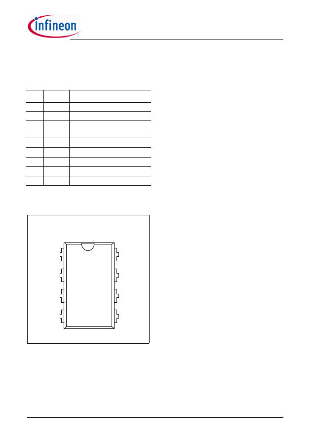
Pin Configuration and Functionality
1
Pin Configuration and Functionality
1.1
Pin Configuration with PG-DIP-8
Pin
Symbol
Function
1
BA
extended Blanking & Auto-restart
2
FB
FeedBack
3
CS
Current Sense/
650V
1)
1)
at T
j
=110°C
CoolMOS
®
Source
4
Drain
650V
1)
CoolMOS
®
Drain
5
Drain
650V
1)
CoolMOS
®
Drain
6
n.c.
Not connected
7
VCC
Controller Supply Voltage
8
GND
Controller GrouND
Package PG-DIP-8
1
6
7
8
4
3
2
5
GND
BA
FB
CS
VCC
n.c.
Drain
Drain
Figure 1
Pin Configuration PG-DIP-8 (top view)
Note: Pin 4 and 5 are shorted
1.2
Pin Functionality
BA (extended Blanking & Auto-restart)
The BA pin combines the functions of extendable
blanking time for over load protection and the external
auto-restart enable. The extendable blanking time
function is to extend the built-in 20 ms blanking time by
adding an external capacitor at BA pin to ground. The
external auto-restart enable function is an external
access to stop the gate switching and force the IC enter
auto-restart mode. It is triggered by pulling down the
BA pin to less than 0.33V.
FB (Feedback)
The information about the regulation is provided by the
FB Pin to the internal Protection Unit and to the internal
PWM-Comparator to control the duty cycle. The FB-
Signal is the only control signal in case of light load at
the Active Burst Mode.
CS (Current Sense)
The Current Sense pin senses the voltage developed
on the series resistor inserted in the source of the
integrated CoolMOS
®
If voltage in CS pin reaches the
internal threshold of the Current Limit Comparator, the
Driver output is immediately switched off. Furthermore
the current information is provided for the PWM-
Comparator to realize the Current Mode.
Drain (Drain of integrated CoolMOS
®
)
Drain pin is the connection to the Drain of the
integrated CoolMOS
®
.
VCC (Power Supply)
VCC pin is the positive supply of the IC. The operating
range is between 10.5V and 25V.
GND (Ground)
GND pin is the ground of the controller.
CoolSET
®
-F3R
ICE3BR1765J
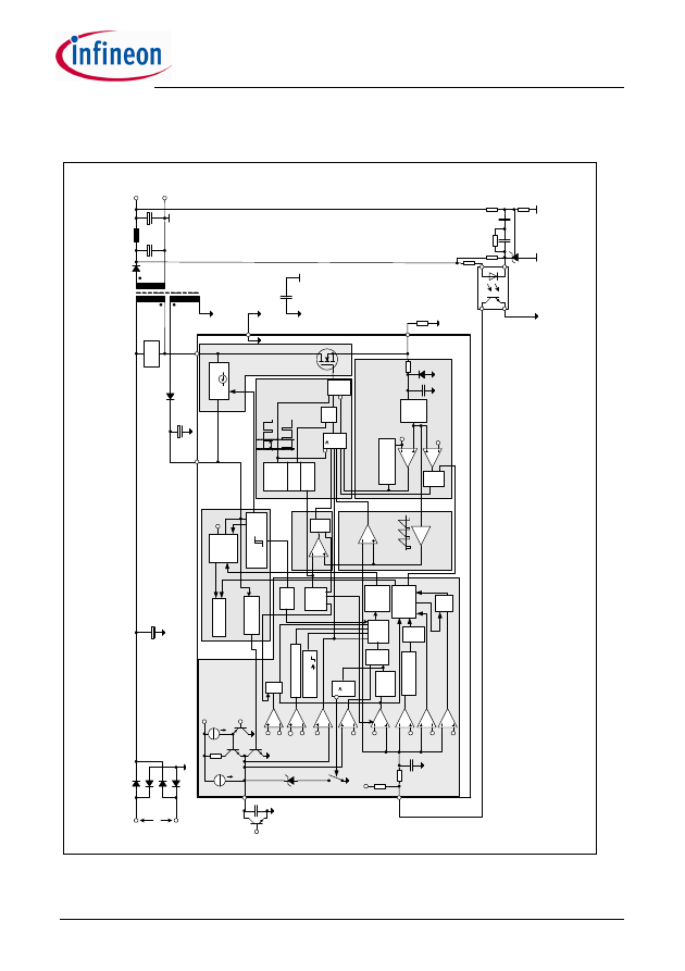
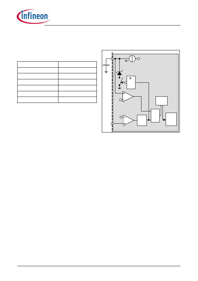
Representative Blockdiagram
Version 2.3
7
19 Nov 2012
2
Representative Blockdiagram
In
te
rn
al
B
ia
s
Vo
lta
ge
Ref
er
e
nce
O
sci
lla
tor
Dut
y Cy
cl
e
ma
x
x3
.3
Cur
re
nt
Li
m
iti
ng
PW
M
O
P
Cu
rr
en
t Mo
de
S
oft
S
ta
rt
C2
C1
20.
5V
25.
5V
R
FB
P
owe
r Man
agem
en
t
C
BK
C
VCC
85 .
..
270 V
A
C
C
Bul
k
+
C
onv
ert
er
D
C
Out
put
V
OUT
PW
M
Co
mpa
rat
or
C3
4.
0V
C4
4.
0V
Ga
te
Dr
iv
er
0.
72
Cl
oc
k
R
S
ense
10
kΩ
D1
C6
a
3.
0
V
C5
1.
35V
C1
0
R
S
Q
A
uto
R
est
ar
t
M
ode
&
G7
&
G5
&
G9
1
G8
& G1
Th
erm
al
Sh
ut
d
own
0.
9V
S1
1
Pow
er
-Do
wn
Res
et
CS
BA
GN
D
VC
C
C7
C8
FB
PW
M
Sect
ion
C
ont
rol
U
ni
t
FF1
C1
2
&
0.
34
V
Le
adi
ng
Edge
B
lan
ki
ng
220
ns
25
kΩ
2p
F
5.
0V
G1
0
1pF
Pr
opa
gat
ion
-D
el
a
y
C
om
pensa
tio
n
5.
0V
U
nder
vol
tag
e Lo
ckou
t
V
csth
G2
-
ICE3BRxx
6
5J /
Coo
lSET
®
™
-F
3R
( J
itt
er M
o
de )
Snu
bber
VC
C
Dr
ai
n
Co
ol
M
O
S
®
S
tartu
p C
ell
C6
b
&
G6
3.
5V
&
G1
1
A
cti
ve
B
ur
st
Mo
de
0.
67V
10.
5V
18
V
#1
#
: opt
ion
al exte
rnal com
p
one
nt
s;
#1 : C
BK
is
us
ed
to
ex
te
nd
th
e B
la
n
ki
ng
T
im
e
#2 : T
AE
is used t
o ena
ble t
he ext
erna
l Au
to
-rest
art f
eat
ure
Fr
eq
. jit
te
r
20
ms
B
lank
ing
Ti
me
20
m
s B
lan
ki
ng
Ti
me
12
0u
s Bl
an
ki
ng
T
im
e
Sof
t
St
ar
t
Bl
oc
k
Sof
t-
S
ta
rt
Co
mp
ara
tor
Spi
ke
B
lank
ing
30u
s
T2
3.
25k
Ω
5.
0V
T1
T3
0.
6V
I
BK
VC
C
A
uto
-r
es
ta
rt
Ena
bl
e
S
ign
al
T
AE
C9
0.
33V
1 ms
coun
ter
T
j
>13
0
°C
#2
Figure 2
Representative Blockdiagram
Version 2.3
8
19 Nov 2012
CoolSET
®
-F3R
ICE3BR1765J
Functional Description
3
Functional Description
All values which are used in the functional description
are typical values. For calculating the worst cases the
min/max values which can be found in section 4
Electrical Characteristics have to be considered.
3.1
Introduction
CoolSET
®
-F3R jitter series (ICE3BRxx65J) is the latest
version of the CoolSET
®
-F3 for the lower power
application. The particular enhanced features are the
built-in features for soft start, blanking window and
frequency jitter. It provides the flexibility to increase the
blanking window by simply addition of a capacitor in BA
pin. In order to further increase the flexibility of the
protection feature, an external auto-restart enable
features are added. Moreover, the proven outstanding
features in CoolSET
®
-F3 are still remained such as the
active burst mode, propagation delay compensation,
modulated gate driving, auto-restart protection for Vcc
overvoltage, over temperature, over load, open loop,
etc.
The intelligent Active Burst Mode can effectively obtain
the lowest Standby Power at light load and no load
conditions. After entering the burst mode, there is still a
full control of the power conversion to the output
through the optocoupler, that is used for the normal
PWM control. The response on load jumps is optimized
and the voltage ripple on V
out
is minimized. The V
out
is
on well controlled in this mode.
The usually external connected RC-filter in the
feedback line after the optocoupler is integrated in the
IC to reduce the external part count.
Furthermore a high voltage Startup Cell is integrated
into the IC which is switched off once the Undervoltage
Lockout on-threshold of 18V is exceeded. This Startup
Cell is part of the integrated CoolMOS
®
. The external
startup resistor is no longer necessary as this Startup
Cell is connected to the Drain. Power losses are
therefore reduced. This increases the efficiency under
light load conditions drastically.
Adopting the BiCMOS technology, it can increase the
design flexibility as the Vcc voltage range is increased
to 25V.
The CoolSET
®
-F3R has a built-in 20ms soft start
function. It can further save external component
counts.
There are 2 modes of blanking time for high load
jumps; the basic mode and the extendable mode. The
blanking time for the basic mode is set at 20ms while
the extendable mode will increase the blanking time by
adding an external capacitor at the BA pin in addition to
the basic mode blanking time. During this blanking time
window the overload detection is disabled. With this
concept no further external components are necessary
to adjust the blanking window.
In order to increase the robustness and safety of the
system, the IC provides Auto Restart protection. The
Auto Restart Mode reduces the average power
conversion to a minimum level under unsafe operating
conditions. This is necessary for a prolonged fault
condition which could otherwise lead to a destruction of
the SMPS over time. Once the malfunction is removed,
normal operation is automatically retained after the
next Start Up Phase. To make the protection more
flexible, an external auto-restart enable pin is provided.
When the pin is triggered, the switching pulse at gate
will stop and the IC enters the auto-restart mode after
the pre-defined spike blanking time.
The internal precise peak current control reduces the
costs for the transformer and the secondary diode. The
influence of the change in the input voltage on the
maximum power limitation can be avoided together
with the integrated Propagation Delay Compensation.
Therefore the maximum power is nearly independent
on the input voltage, which is required for wide range
SMPS. Thus there is no need for the over-sizing of the
SMPS, e.g. the transformer and the output diode.
Furthermore, this F3R series implements the
frequency jitter mode to the switching clock such that
the EMI noise will be effectively reduced.
3.2
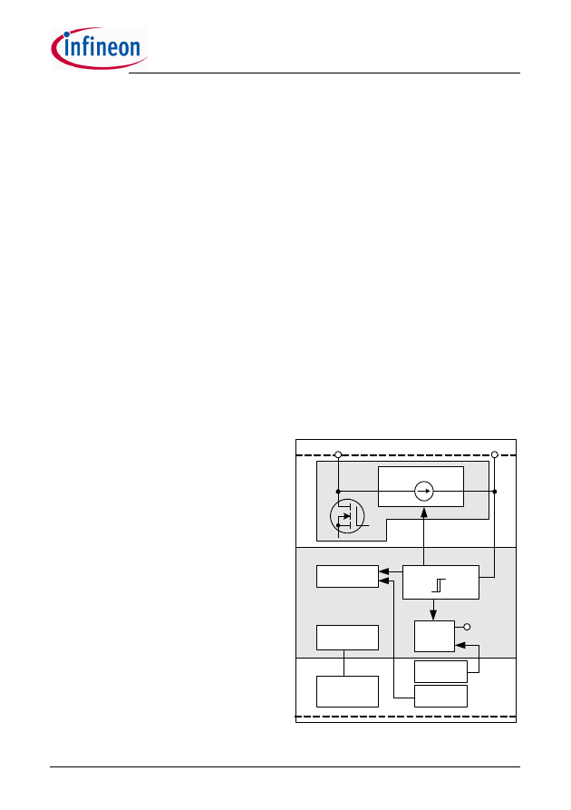
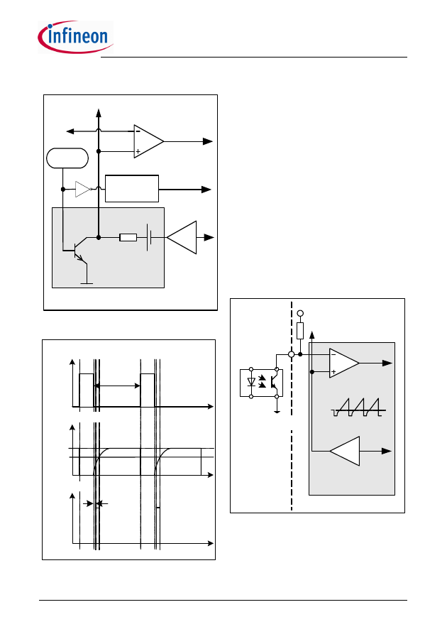
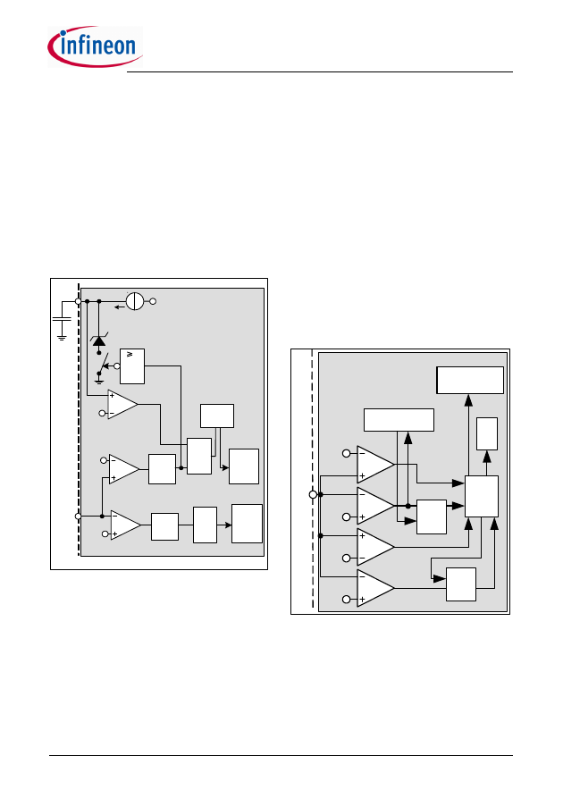
Power Management
Internal Bias
Voltage
Reference
Power Management
5.0V
Undervoltage Lockout
18V
10.5V
Power-Down Reset
Active Burst
Mode
Auto Restart
Mode
Startup Cell
VCC
Drain
Depl. CoolMOS™
Soft Start block
Figure 3
Power Management
CoolSET
®
-F3R
ICE3BR1765J
Functional Description
Version 2.3
9
19 Nov 2012
The Undervoltage Lockout monitors the external
supply voltage V
VCC
. When the SMPS is plugged to the
main line the internal Startup Cell is biased and starts
to charge the external capacitor C
VCC
which is
connected to the VCC pin. This VCC charge current is
controlled to 0.9mA by the Startup Cell. When the V
VCC
exceeds the on-threshold V
CCon
=18V the bias circuit
are switched on. Then the Startup Cell is switched off
by the Undervoltage Lockout and therefore no power
losses present due to the connection of the Startup Cell
to the Drain voltage. To avoid uncontrolled ringing at
switch-on, a hysteresis start up voltage is implemented.
The switch-off of the controller can only take place
when V
VCC
falls below 10.5V after normal operation
was entered. The maximum current consumption
before the controller is activated is about 150
μA.
When V
VCC
falls below the off-threshold V
CCoff
=10.5V,
the bias circuit is switched off and the soft start counter
is reset. Thus it is ensured that at every startup cycle
the soft start starts at zero.
The internal bias circuit is switched off if Auto Restart
Mode is entered. The current consumption is then
reduced to 150
μA.
Once the malfunction condition is removed, this block
will then turn back on. The recovery from Auto Restart
Mode does not require re-cycling the AC line.
When Active Burst Mode is entered, the internal Bias is
switched off most of the time but the Voltage Reference
is kept alive in order to reduce the current consumption
below 450
μA.
3.3
Improved Current Mode
x3.3
PWM OP
Improved
Current Mode
0.67V
C8
PWM-Latch
CS
FB
R
S
Q
Q
Driver
Soft-Start Comparator
Figure 4
Current Mode
Current Mode means the duty cycle is controlled by the
slope of the primary current. This is done by comparing
the FB signal with the amplified current sense signal.
t
FB
Amplified Current Signal
t
on
t
0.67V
Driver
Figure 5
Pulse Width Modulation
In case the amplified current sense signal exceeds the
FB signal the on-time T
on
of the driver is finished by
resetting the PWM-Latch (see Figure 5).
The primary current is sensed by the external series
resistor R
Sense
inserted in the source of the integrated
CoolMOS
®
. By means of Current Mode regulation, the
secondary output voltage is insensitive to the line
variations. The current waveform slope will change with
the line variation, which controls the duty cycle.
The external R
Sense
allows an individual adjustment of
the maximum source current of the integrated
CoolMOS
®
.
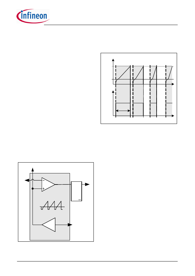
To improve the Current Mode during light load
conditions the amplified current ramp of the PWM-OP
is superimposed on a voltage ramp, which is built by
the switch T2, the voltage source V1 and a resistor R1
(see Figure 6). Every time the oscillator shuts down for
maximum duty cycle limitation the switch T2 is closed
by V
OSC
. When the oscillator triggers the Gate Driver,
T2 is opened so that the voltage ramp can start.
In case of light load the amplified current ramp is too
small to ensure a stable regulation. In that case the
Voltage Ramp is a well defined signal for the
comparison with the FB-signal. The duty cycle is then
controlled by the slope of the Voltage Ramp.
By means of the time delay circuit which is triggered by
the inverted V
OSC
signal, the Gate Driver is switched-off
until it reaches approximately 156ns delay time (see
Figure 7). It allows the duty cycle to be reduced
continuously till 0% by decreasing V
FB
below that
threshold.
PWM OP
0.67V
10k
Ω
Oscillator
C8
T
2
R
1
C
1
FB
PWM-Latch
V
1
Gate Driver
Voltage Ramp
V
OSC
Soft-Start Comparator
time delay
circuit (156ns)
X3.3
PWM Comparator
CoolSET
®
-F3R
ICE3BR1765J
Functional Description
Version 2.3
10
19 Nov 2012
Figure 6
Improved Current Mode
t
t
V
OSC
0.67V
FB
t
max.
Duty Cycle
Gate Driver
Voltage Ramp
156ns time delay
Figure 7
Light Load Conditions
3.3.1
PWM-OP
The input of the PWM-OP is applied over the internal
leading edge blanking to the external sense resistor
R
Sense
connected to pin CS. R
Sense
converts the source
current into a sense voltage. The sense voltage is
amplified with a gain of 3.3 by PWM OP. The output of
the PWM-OP is connected to the voltage source V
1
.
The voltage ramp with the superimposed amplified
current signal is fed into the positive inputs of the PWM-
Comparator C8 and the Soft-Start-Comparator (see
Figure 6).
3.3.2
PWM-Comparator
The PWM-Comparator compares the sensed current
signal of the integrated CoolMOS
®
with the feedback
signal V
FB
(see Figure 8). V
FB
is created by an external
optocoupler or external transistor in combination with
the internal pull-up resistor R
FB
and provides the load
information of the feedback circuitry. When the
amplified current signal of the integrated CoolMOS
®
exceeds the signal V
FB
the PWM-Comparator switches
off the Gate Driver.
X3.3
PWM OP
Improved
Current Mode
PWM Comparator
CS
Soft-Start Comparator
5V
C8
0.67V
FB
Optocoupler
R
FB
PWM-Latch
Figure 8
PWM Controlling
CoolSET
®
-F3R
ICE3BR1765J
Functional Description
Version 2.3
11
19 Nov 2012
3.4
Startup Phase
S o ft-S ta rt
C o m p a ra to r
S o ft S ta rt
&
G 7
C 7
G a te D riv e r
0 .6 7 V
x 3 .3
P W M O P
C S
S o ft S ta rt c o u n te r
S o ft S ta rt
S
oft
St
ar
t f
inis
h
S o ftS
Figure 9
Soft Start
In the Startup Phase, the IC provides a Soft Start
period to control the primary current by means of a duty
cycle limitation. The Soft Start function is a built-in
function and it is controlled by an internal counter.
.
V
SoftS
V
SoftS2
V
SoftS1
Figure 10
Soft Start Phase
When the V
VCC
exceeds the on-threshold voltage, the
IC starts the Soft Start mode (see Figure 10).
The function is realized by an internal Soft Start
resistor, an current sink and a counter. And the
amplitude of the current sink is controlled by the
counter (see Figure 11).
5V
R
SoftS
Soft Start
Counter
I
2I
4I
SoftS
8I
32I
Figure 11
Soft Start Circuit
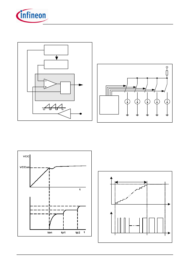
After the IC is switched on, the V
SFOFTS
voltage is
controlled such that the voltage is increased step-
wisely (32 steps) with the increase of the counts. The
Soft Start counter would send a signal to the current
sink control in every 600us such that the current sink
decrease gradually and the duty ratio of the gate drive
increases gradually. The Soft Start will be finished in
20ms (t
Soft-Start
) after the IC is switched on. At the end of
the Soft Start period, the current sink is switched off.
t
V
SOFTS32
V
SoftS
Gate
Driver
t
t
Soft-Start
Figure 12 Gate drive signal under Soft-Start Phase
CoolSET
®
-F3R
ICE3BR1765J
Functional Description
Version 2.3
12
19 Nov 2012
Within the soft start period, the duty cycle is increasing
from zero to maximum gradually (see Figure 12).
In addition to Start-Up, Soft-Start is also activated at
each restart attempt during Auto Restart.
t
t
V
SoftS
t
V
SOFTS32
4.0V
t
Soft-Start
V
OUT
V
FB
V
OUT
t
Start-Up
Figure 13 Start Up Phase
The Start-Up time t
Start-Up
before the converter output
voltage V
OUT
is settled, must be shorter than the Soft-
Start Phase t
Soft-Start
(see Figure 13).
By means of Soft-Start there is an effective
minimization of current and voltage stresses on the
integrated CoolMOS
®
, the clamp circuit and the output
overshoot and it helps to prevent saturation of the
transformer during Start-Up.
3.5
PWM Section
Oscillator
Duty Cycle
max
Gate Driver
0.75
Clock
&
G9
1
G8
PWM Section
FF1
R
S
Q
Soft Start
Comparator
PWM
Comparator
Current
Limiting
CoolMOS
®
Gate
Frequency
Jitter
Soft Start
Block
Figure 14
PWM Section Block
3.5.1
Oscillator
The oscillator generates a fixed frequency of 65KHz
with frequency jittering of ±4% (which is ±2.6KHz) at a
jittering period of 4ms.
A capacitor, a current source and current sink which
determine the frequency are integrated. In order to
achieve a very accurate switching frequency, the
charging and discharging current of the implemented
oscillator capacitor are internally trimmed. The ratio of
controlled charge to discharge current is adjusted to
reach a maximum duty cycle limitation of D
max
=0.75.
Once the Soft Start period is over and when the IC goes
into normal operating mode, the switching frequency of
the clock is varied by the control signal from the Soft
Start block. Then the switching frequency is varied in
range of 65KHz ± 2.6KHz at period of 4ms.
3.5.2
PWM-Latch FF1
The output of the oscillator block provides continuous
pulse to the PWM-Latch which turns on/off the
integrated CoolMOS
®
. After the PWM-Latch is set, it is
reset by the PWM comparator, the Soft Start
comparator or the Current -Limit comparator. When it is
in reset mode, the output of the driver is shut down
immediately.
CoolSET
®
-F3R
ICE3BR1765J
Functional Description
Version 2.3
13
19 Nov 2012
3.5.3
Gate Driver
VCC
1
PWM-Latch
CoolMOS
®
Gate Driver
Gate
Figure 15
Gate Driver
The driver-stage is optimized to minimize EMI and to
provide high circuit efficiency. The switch on speed is
slowed down before it reaches the integrated
CoolMOS
®
turn on threshold. That is a slope control of
the rising edge at the output of the driver (see Figure
16).
t
(internal)
V
Gate
5V
ca. t = 130ns
Figure 16
Gate Rising Slope
Thus the leading switch on spike is minimized.
Furthermore the driver circuit is designed to eliminate
cross conduction of the output stage.
During power up, when VCC is below the undervoltage
lockout threshold V
VCCoff
, the output of the Gate Driver
is set to low in order to disable power transfer to the
secondary side.
3.6
Current Limiting
Current Limiting
C10
C12
&
0.34V
Leading
Edge
Blanking
220ns
G10
Propagation-Delay
Compensation
V
csth
Active Burst
Mode
PWM Latch
FF1
10k
D1
1pF
PWM-OP
CS
Figure 17
Current Limiting Block
There is a cycle by cycle peak current limiting operation
realized by the Current-Limit comparator C10. The
source current of the integrated CoolMOS
®
is sensed
via an external sense resistor R
Sense
. By means of
R
Sense
the source current is transformed to a sense
voltage V
Sense
which is fed into the CS pin. If the voltage
V
Sense
exceeds the internal threshold voltage V
csth,
the
comparator C10 immediately turns off the gate drive by
resetting the PWM Latch FF1.
A Propagation Delay Compensation is added to
support the immediate shut down of the integrated
CoolMOS
®
with very short propagation delay. Thus the
influence of the AC input voltage on the maximum
output power can be reduced to minimal.
In order to prevent the current limit from distortions
caused by leading edge spikes, a Leading Edge
Blanking is integrated in the current sense path for the
comparators C10, C12 and the PWM-OP.
The output of comparator C12 is activated by the Gate
G10 if Active Burst Mode is entered. When it is
activated, the current limiting is reduced to 0.34V. This
voltage level determines the maximum power level in
Active Burst Mode.
CoolSET
®
-F3R
ICE3BR1765J
Functional Description
Version 2.3
14
19 Nov 2012
3.6.1
Leading Edge Blanking
t
V
Sense
V
csth
t
LEB
= 220ns
Figure 18
Leading Edge Blanking
Whenever the integrated CoolMOS
®
is switched on, a
leading edge spike is generated due to the primary-
side capacitances and reverse recovery time of the
secondary-side rectifier. This spike can cause the gate
drive to switch off unintentionally. In order to avoid a
premature termination of the switching pulse, this spike
is blanked out with a time constant of t
LEB
= 220ns.
3.6.2
Propagation Delay Compensation
In case of over-current detection, there is always
propagation delay to switch off the integrated
CoolMOS
®
. An overshoot of the peak current I
peak
is
induced to the delay, which depends on the ratio of dI/
dt of the peak current (see Figure 19).
t
I
Sense
I
Limit
t
Propagation Delay
I
Overshoot1
I
peak1
Signal1
Signal2
I
Overshoot2
I
peak2
Figure 19
Current Limiting
The overshoot of Signal2 is larger than of Signal1 due
to the steeper rising waveform. This change in the
slope depends on the AC input voltage. Propagation
Delay Compensation is integrated to reduce the
overshoot due to dI/dt of the rising primary current.
Thus the propagation delay time between exceeding
the current sense threshold V
csth
and the switching off
of the integrated CoolMOS
®
is compensated over
temperature within a wide range. Current Limiting is
then very accurate.
For example, I
peak
= 0.5A with R
Sense
= 2. The current
sense threshold is set to a static voltage level V
csth
=1V
without Propagation Delay Compensation. A current
ramp of dI/dt = 0.4A/µs, or dV
Sense
/dt = 0.8V/µs, and a
propagation delay time of t
Propagation Delay
=180ns leads
to an I
peak
overshoot of 14.4%. With the propagation
delay compensation, the overshoot is only around 2%
(see Figure 20).
0,9
0,95
1
1,05
1,1
1,15
1,2
1,25
1,3
0
0,2
0,4
0,6
0,8
1
1,2
1,4
1,6
1,8
2
with compensation
without compensation
dt
dV
Sense
s
V
μ
Sen
se
V
V
Figure 20
Overcurrent Shutdown
The Propagation Delay Compensation is realized by
means of a dynamic threshold voltage V
csth
(see Figure
21). In case of a steeper slope the switch off of the
driver is earlier to compensate the delay.
t
V
csth
V
OSC
Signal1
Signal2
V
Sense
Propagation Delay
max. Duty Cycle
off time
t
Figure 21
Dynamic Voltage Threshold V
csth
CoolSET
®
-F3R
ICE3BR1765J
Functional Description
Version 2.3
15
19 Nov 2012
3.7
Control Unit
The Control Unit contains the functions for Active Burst
Mode and Auto Restart Mode. The Active Burst Mode
and the Auto Restart Mode both have 20ms internal
Blanking Time. For the Auto Restart Mode, a further
extendable Blanking Time is achieved by adding
external capacitor at BA pin. By means of this Blanking
Time, the IC avoids entering into these two modes
accidentally. Furthermore those buffer time for the
overload detection is very useful for the application that
works in low current but requires a short duration of
high current occasionally.
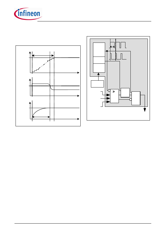
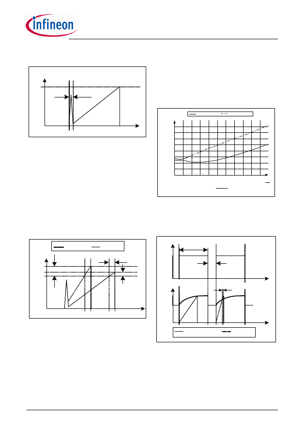
3.7.1
Basic and Extendable Blanking Mode
C3
4.0V
C4
4.0V
C5
1.35V
&
G5
&
G6
0.9V
S1
1
G2
Control Unit
Active
Burst
Mode
Auto
Restart
Mode
5.0V
BA
FB
C
BK
20ms
Blanking
Time
20ms
Blanking
Time
Spike
Blanking
30us
#
I
BK
Figure 22
Basic and Extendable Blanking Mode
There are 2 kinds of Blanking mode; basic mode and
the extendable mode. The basic mode is just an
internal set 20ms blanking time while the extendable
mode has an extra blanking time by connecting an
external capacitor to the BA pin in addition to the pre-
set 20ms blanking time. For the extendable mode, the
gate G5 is blocked even though the 20ms blanking time
is reached if an external capacitor C
BK
is added to BA
pin. While the 20ms blanking time is passed, the switch
S1 is opened by G2. Then the 0.9V clamped voltage at
BA pin is charged to 4.0V through the internal I
BK
constant current. G5 is enabled by comparator C3.
After the 30us spike blanking time, the Auto Restart
Mode is activated.
For example, if C
BK
= 0.22uF, I
BK
= 13uA
Blanking time = 20ms + C
BK
x (4.0 - 0.9) / I
BK
= 72ms
In order to make the startup properly, the maximum C
BK
capacitor is restricted to less than 0.65uF.
The Active Burst Mode has basic blanking mode only
while the Auto Restart Mode has both the basic and the
extendable blanking mode.
3.7.2
Active Burst Mode
The IC enters Active Burst Mode under low load
conditions. With the Active Burst Mode, the efficiency
increases significantly at light load conditions while still
maintaining a low ripple on V
OUT
and a fast response on
load jumps. During Active Burst Mode, the IC is
controlled by the FB signal. Since the IC is always
active, it can be a very fast response to the quick
change at the FB signal. The Start up Cell is kept OFF
in order to minimize the power loss.
C4
4.0V
C6a
3.5V
C5
1.35V
FB
Control Unit
Active
Burst
Mode
Internal Bias
&
G10
Current
Limiting
&
G6
C6b
3.0V
&
G11
20 ms Blanking
Time
Figure 23
Active Burst Mode
The Active Burst Mode is located in the Control Unit.
Figure 23 shows the related components.
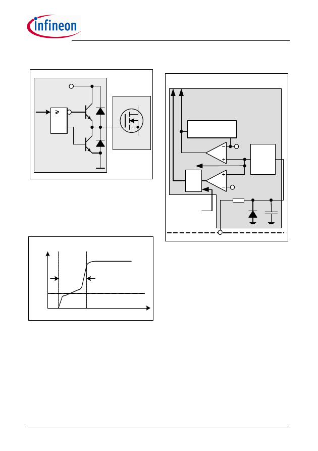
3.7.2.1
Entering Active Burst Mode
The FB signal is kept monitoring by the comparator C5.
During normal operation, the internal blanking time
counter is reset to 0. Once the FB signal falls below
1.35V, it starts to count. When the counter reach 20ms
CoolSET
®
-F3R
ICE3BR1765J
Functional Description
Version 2.3
16
19 Nov 2012
and FB signal is still below 1.35V, the system enters
the Active Burst Mode. This time window prevents a
sudden entering into the Active Burst Mode due to
large load jumps.
After entering Active Burst Mode, a burst flag is set and
the internal bias is switched off in order to reduce the
current consumption of the IC to approx. 450uA.
It needs the application to enforce the VCC voltage
above the Undervoltage Lockout level of 10.5V such
that the Startup Cell will not be switched on
accidentally. Or otherwise the power loss will increase
drastically. The minimum VCC level during Active Burst
Mode depends on the load condition and the
application. The lowest VCC level is reached at no load
condition.
3.7.2.2
Working in Active Burst Mode
After entering the Active Burst Mode, the FB voltage
rises as V
OUT
starts to decrease, which is due to the
inactive PWM section. The comparator C6a monitors
the FB signal. If the voltage level is larger than 3.5V, the
internal circuit will be activated; the Internal Bias circuit
resumes and starts to provide switching pulse. In
Active Burst Mode the gate G10 is released and the
current limit is reduced to 0.34V, which can reduce the
conduction loss and the audible noise. If the load at
V
OUT
is still kept unchanged, the FB signal will drop to
3.0V. At this level the C6b deactivates the internal
circuit again by switching off the internal Bias. The gate
G11 is active again as the burst flag is set after entering
Active Burst Mode. In Active Burst Mode, the FB
voltage is changing like a saw tooth between 3.0V and
3.5V (see figure 24).
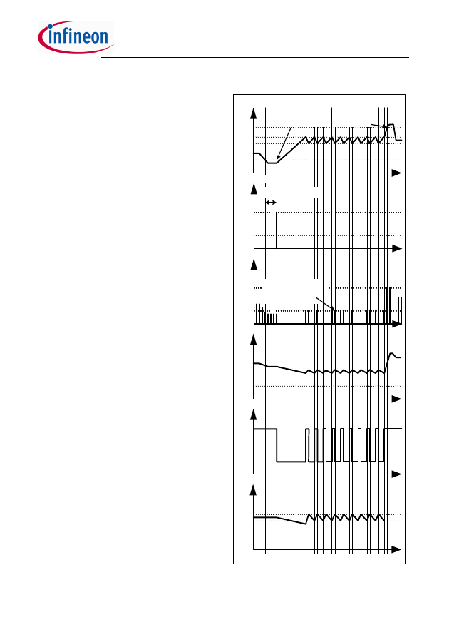
3.7.2.3
Leaving Active Burst Mode
The FB voltage will increase immediately if there is a
high load jump. This is observed by the comparator C4.
Since the current limit is app. 34% during Active Burst
Mode, it needs a certain load jump to rise the FB signal
to exceed 4.0V. At that time the comparator C4 resets
the Active Burst Mode control which in turn blocks the
comparator C12 by the gate G10. The maximum
current can then be resumed to stabilize the V
OUT.
1.35V
3.5V
4.0V
V
FB
t
t
0.34V
1.03V
V
CS
10.5V
V
VCC
t
t
450uA
I
VCC
t
2.7mA
V
OUT
t
20ms Blanking Time
Current limit level
during Active Burst
Mode
3.0V
Entering
Active Burst
Mode
Leaving
Active Burst
Mode
Blanking Timer
Figure 24
Signals in Active Burst Mode
CoolSET
®
-F3R
ICE3BR1765J
Functional Description
Version 2.3
17
19 Nov 2012
3.7.3
Protection Modes
The IC provides Auto Restart Mode as the protection
feature. Auto Restart mode can prevent the SMPS from
destructive states. The following table shows the
relationship between possible system failures and the
corresponding protection modes.
VCC Overvoltage
Auto Restart Mode
Overtemperature
Auto Restart Mode
Overload
Auto Restart Mode
Open Loop
Auto Restart Mode
VCC Undervoltage
Auto Restart Mode
Short Optocoupler
Auto Restart Mode
Auto restart enable
Auto Restart Mode
Before entering the Auto Restart protection mode,
some of the protections can have extended blanking
time to delay the protection and some needs to fast
react and will go straight to the protection. Overload
and open loop protection are the one can have
extended blanking time while Vcc Overvoltage, Over
temperature, Vcc Undervoltage, short opto-coupler
and external auto restart enable will go to protection
right away.
After the system enters the Auto-restart mode, the IC
will be off. Since there is no more switching, the Vcc
voltage will drop. When it hits the Vcc turn off threshold,
the start up cell will turn on and the Vcc is charged by
the startup cell current to Vcc turn on threshold. The IC
is on and the startup cell will turn off. At this stage, it will
enter the startup phase (soft start) with switching
cycles. After the Start Up Phase, the fault condition is
checked. If the fault condition persists, the IC will go to
auto restart mode again. If, otherwise, the fault is
removed, normal operation is resumed.
3.7.3.1
Auto Restart mode with extended
blanking time
Figure 25
Auto Restart Mode
In case of Overload or Open Loop, the FB exceeds
4.0V which will be observed by comparator C4. Then
the internal blanking counter starts to count. When it
reaches 20ms, the switch S1 is released. Then the
clamped voltage 0.9V at V
BA
can increase. When there
is no external capacitor C
BK
connected, the V
BA
will
reach 4.0V immediately. When both the input signals at
AND gate G5 is positive, the Auto Restart Mode will be
activated after the extra spike blanking time of 30us is
elapsed. However, when an extra blanking time is
needed, it can be achieved by adding an external
capacitor, C
BK
. A constant current source of I
BK
will start
to charge the capacitor C
BK
from 0.9V to 4.0V after the
switch S1 is released. The charging time from 0.9V to
4.0V are the extendable blanking time. If C
BK
is 0.22uF
and I
BK
is 13uA, the extendable blanking time is around
52ms and the total blanking time is 72ms. In combining
the FB and blanking time, there is a blanking window
generated which prevents the system to enter Auto
Restart Mode due to large load jumps.
C3
4.0V
C4
4.0V
&
G5
0.9V
S1
1
G2
Control Unit
Auto
Restart
Mode
5.0V
BA
FB
C
BK
20ms
Blanking
Time
Spike
Blanking
30us
#
I
BK
C1
20.5V
Spike
Blanking
30us
&
G1
Thermal Shutdown
T
j
>140°C
Auto Restart
mode
VCC
C4
4.0V
Voltage
Reference
Control Unit
Auto Restart
Mode Reset
V
VCC
< 10.5V
FB
C2
120us
Blanking
Time
VCC
25.5V
softs_period
BA
Auto-restart
Enable
Signal
T
AE
C9
8us
Blanking
Time
0.3V
Stop
gate
drive
1ms
counter
UVLO
CoolSET
®
-F3R
ICE3BR1765J
Functional Description
Version 2.3
18
19 Nov 2012
3.7.3.2
Auto Restart without extended blanking
time
Figure 26
Auto Restart mode
There are 2 modes of V
CC
overvoltage protection; one
is during soft start and the other is at all conditions.
The first one is V
VCC
voltage is > 20.5V and FB is > 4.0V
and during soft_start period and the IC enters Auto
Restart Mode. The VCC voltage is observed by
comparator C1 and C4. The fault conditions are to
detect the abnormal operating during start up such as
open loop during light load start up, etc. The logic can
eliminate the possible of entering Auto Restart mode if
there is a small voltage overshoots of V
VCC
during
normal operating.
The 2nd one is V
VCC
>25.5V and last for 120us and the
IC enters Auto Restart Mode. This 25.5V Vcc OVP
protection is inactivated during burst mode.
The Thermal Shutdown block monitors the junction
temperature of the IC. After detecting a junction
temperature higher than 130°C, the Auto Restart Mode
is entered.
In case the pre-defined auto-restart features are not
sufficient, there is a customer defined external Auto-
restart Enable feature. This function can be triggered
by pulling down the BA pin to < 0.33V. It can simply add
a trigger signal to the base of the externally added
transistor, T
AE
at the BA pin. When the function is
enabled, the gate drive switching will be stopped and
then the IC will enter auto-restart mode if the signal
persists. To ensure this auto-restart function will not be
mis-triggered during start up, a 1ms delay time is
implemented to blank the unstable signal.
VCC undervoltage is the Vcc voltage drop below Vcc
turn off threshold. Then the IC will turn off and the start
up cell will turn on automatically. And this leads to Auto
Restart Mode.
Short Optocoupler also leads to VCC undervoltage as
there is no self supply after activating the internal
reference and bias.

CoolSET
®
-F3R
ICE3BR1765J
Electrical Characteristics
Version 2.3
19
19 Nov 2012
4
Electrical Characteristics
Note:
All voltages are measured with respect to ground (Pin 5). The voltage levels are valid if other ratings are
not violated.
4.1
Absolute Maximum Ratings
Parameter
Symbol
Limit Values
Unit
Remarks
min.
max.
Switching drain current, pulse width t
p
limited by T
j
=150°C
I
s
-
4.03
A
Pulse drain current, pulse width t
p
limited
by T
j
=150°C
I
D_Puls
-
6.12
A
Avalanche energy, repetitive t
AR
limited by
max. T
j
=150°C
1)
1)
Repetitive avalanche causes additional power losses that can be calculated as P
AV
=E
AR
*f
E
AR
-
0.15
mJ
Avalanche current, repetitive t
AR
limited by
max. T
j
=150°C
1)
I
AR
-
1.5
A
VCC Supply Voltage
V
VCC
-0.3
27
V
FB Voltage
V
FB
-0.3
5.5
V
BA Voltage
V
BA
-0.3
5.5
V
CS Voltage
V
CS
-0.3
5.5
V
Junction Temperature
T
j
-40
150
°C
Controller & CoolMOS
®
Storage Temperature
T
S
-55
150
°C
Thermal Resistance
Junction -Ambient
R
thJA
-
90
K/W
Soldering temperature, wavesoldering
only allowed at leads
T
sold
-
260
°C
1.6mm (0.063in.) from
case for 10s
ESD Capability (incl. Drain Pin)
V
ESD
-
2
kV
Human body model
2)
2)
According to EIA/JESD22-A114-B (discharging a 100pF capacitor through a 1.5k
Ω series resistor)
Note:
Absolute maximum ratings are defined as ratings, which when being exceeded may lead to destruction
of the integrated circuit. For the same reason make sure, that any capacitor that will be connected to pin 4
(VCC) is discharged before assembling the application circuit.T
a
=25
°C unless otherwise specified.

CoolSET
®
-F3R
ICE3BR1765J
Electrical Characteristics
Version 2.3
20
19 Nov 2012
4.2
Operating Range
Note:
Within the operating range the IC operates as described in the functional description.
Parameter
Symbol
Limit Values
Unit
Remarks
min.
max.
VCC Supply Voltage
V
VCC
V
VCCoff
25
V
Max value limited due to Vcc OVP
Junction Temperature of
Controller
T
jCon
-25
130
°C
Max value limited due to thermal
shut down of controller
Junction Temperature of
CoolMOS
®
T
jCoolMOS
-25
150
°C
4.3
Characteristics
4.3.1
Supply Section
Note:
The electrical characteristics involve the spread of values within the specified supply voltage and junction
temperature range T
J
from – 25
°C to 125 °C. Typical values represent the median values, which are
related to 25°C. If not otherwise stated, a supply voltage of V
CC
= 18 V is assumed.
Parameter
Symbol
Limit Values
Unit
Test Condition
min.
typ.
max.
Start Up Current
I
VCCstart
-
150
250
μA
V
VCC
=17V
VCC Charge Current
I
VCCcharge1
-
-
5.0
mA
V
VCC
= 0V
I
VCCcharge2
0.55
0.9
1.60
mA
V
VCC
= 1V
I
VCCcharge3
-
0.7
-
mA
V
VCC
=17V
Leakage Current of
Start Up Cell and CoolMOS
®
I
StartLeak
-
0.2
50
μA
V
Drain
= 450V
at T
j
=100°C
Supply Current with
Inactive Gate
I
VCCsup1
-
1.5
2.5
mA
Supply Current with Active Gate
I
VCCsup2
-
2.7
3.4
mA
I
FB
= 0A
Supply Current in
Auto Restart Mode with Inactive
Gate
I
VCCrestart
-
250
-
μA
I
FB
= 0A
Supply Current in Active Burst
Mode with Inactive Gate
I
VCCburst1
-
450
950
μA
V
FB
= 2.5V
I
VCCburst2
-
450
950
μA
V
VCC
= 11.5V,V
FB
= 2.5V
VCC Turn-On Threshold
VCC Turn-Off Threshold
VCC Turn-On/Off Hysteresis
V
VCCon
V
VCCoff
V
VCChys
17.0
9.8
-
18.0
10.5
7.5
19.0
11.2
-
V
V
V

Version 2.3
21
19 Nov 2012
CoolSET
®
-F3R
ICE3BR1765J
Electrical Characteristics
4.3.2
Internal Voltage Reference
Parameter
Symbol
Limit Values
Unit
Test Condition
min.
typ.
max.
Trimmed Reference Voltage
V
REF
4.90
5.00
5.10
V
measured at pin FB
I
FB
= 0
4.3.3
PWM Section
Parameter
Symbol
Limit Values
Unit
Test Condition
min.
typ.
max.
Fixed Oscillator Frequency
f
OSC1
56.5
65.0
73.5
kHz
f
OSC2
59.8
65.0
70.2
kHz
T
j
= 25°C
Frequency Jittering Range
f
jitter
-
±2.6
-
kHz
T
j
= 25°C
Frequency Jittering period
T
jitter
-
4.0
-
ms
T
j
= 25°C
Max. Duty Cycle
D
max
0.70
0.75
0.80
Min. Duty Cycle
D
min
0
-
-
V
FB
< 0.3V
PWM-OP Gain
A
V
3.1
3.3
3.5
Voltage Ramp Offset
V
Offset-Ramp
-
0.67
-
V
V
FB
Operating Range Min Level V
FBmin
-
0.5
-
V
V
FB
Operating Range Max level V
FBmax
-
-
4.3
V
CS=1V, limited by
Comparator C4
1)
1)
The parameter is not subjected to production test - verified by design/characterization
FB Pull-Up Resistor
R
FB
9
15.4
22
k
Ω
4.3.4
Soft Start time
Parameter
Symbol
Limit Values
Unit
Test Condition
min.
typ.
max.
Soft Start time
t
SS
-
20.0
-
ms

CoolSET
®
-F3R
ICE3BR1765J
Electrical Characteristics
Version 2.3
22
19 Nov 2012
4.3.5
Control Unit
Parameter
Symbol
Limit Values
Unit
Test Condition
min.
typ.
max.
Clamped V
BA
voltage during
Normal Operating Mode
V
BAclmp
0.85
0.9
0.95
V
V
FB
= 4V
Blanking time voltage limit for
Comparator C3
V
BKC3
3.85
4.00
4.15
V
Over Load & Open Loop Detection
Limit for Comparator C4
V
FBC4
3.85
4.00
4.15
V
Active Burst Mode Level for
Comparator C5
V
FBC5
1.25
1.35
1.45
V
Active Burst Mode Level for
Comparator C6a
V
FBC6a
3.35
3.50
3.65
V
After Active Burst
Mode is entered
Active Burst Mode Level for
Comparator C6b
V
FBC6b
2.88
3.00
3.12
V
After Active Burst
Mode is entered
Overvoltage Detection Limit for
Comparator C1
V
VCCOVP1
19.5
20.5
21.5
V
V
FB
= 5V
Overvoltage Detection Limit for
Comparator C2
V
VCCOVP2
25.0
25.5
26.5
V
Auto-restart Enable level at BA pin V
AE
0.25
0.33
0.4
V
>30
μs
Charging current at BA pin
I
BK
10.0
13.0
16.9
μA
Charge starts after the
built-in 20ms blanking
time elapsed
Thermal Shutdown
1)
1)
The parameter is not subjected to production test - verified by design/characterization. The thermal shutdown
temperature refers to the junction temperature of the controller.
T
jSD
130
140
150
°C
Controller
Built-in Blanking Time for
Overload Protection or enter
Active Burst Mode
t
BK
-
20
-
ms
without external
capacitor at BA pin
Inhibit Time for Auto-Restart
enable function during start up
t
IHAE
-
1.0
-
ms
Count when VCC>18V
Spike Blanking Time before Auto-
Restart Protection
t
Spike
-
30
-
μs
Note:
The trend of all the voltage levels in the Control Unit is the same regarding the deviation except V
VCCOVP
.

CoolSET
®
-F3R
ICE3BR1765J
Electrical Characteristics
Version 2.3
23
19 Nov 2012
4.3.6
Current Limiting
Parameter
Symbol
Limit Values
Unit
Test Condition
min.
typ.
max.
Peak Current Limitation
(incl. Propagation Delay)
V
csth
0.96
1.03
1.10
V
dV
sense
/ dt = 0.6V/
μs
(see Figure 20)
Peak Current Limitation during
Active Burst Mode
V
CS2
0.29
0.34
0.38
V
Leading Edge Blanking
t
LEB
-
220
-
ns
CS Input Bias Current
I
CSbias
-1.5
-0.2
-
μA
V
CS
=0V
4.3.7
CoolMOS
®
Section
Parameter
Symbol
Limit Values
Unit
Test Condition
min.
typ.
max.
Drain Source Breakdown Voltage
V
(BR)DSS
650
-
-
V
T
j
= 110°C
Refer to Figure 30 for
other V
(BR)DSS
in
different T
j
Drain Source On-Resistance
R
DSon
-
-
1.70
3.57
1.96
4.12
Ω
Ω
T
j
= 25°C
T
j
=125°C
1)
1)
The parameter is not subjected to production test - verified by design/characterization
at I
D
= 1.5A
Effective output capacitance, energy
related
C
o(er)
-
11.63
-
pF
V
DS
= 0V to 480V
1)
Rise Time
t
rise
-
30
2)
2)
Measured in a Typical Flyback Converter Application
-
ns
Fall Time
t
fall
-
30
2)
-
ns
CoolSET
®
-F3R
ICE3BR1765J
Typical CoolMOS
®
Performance Characteristic
Version 2.3
24
19 Nov 2012
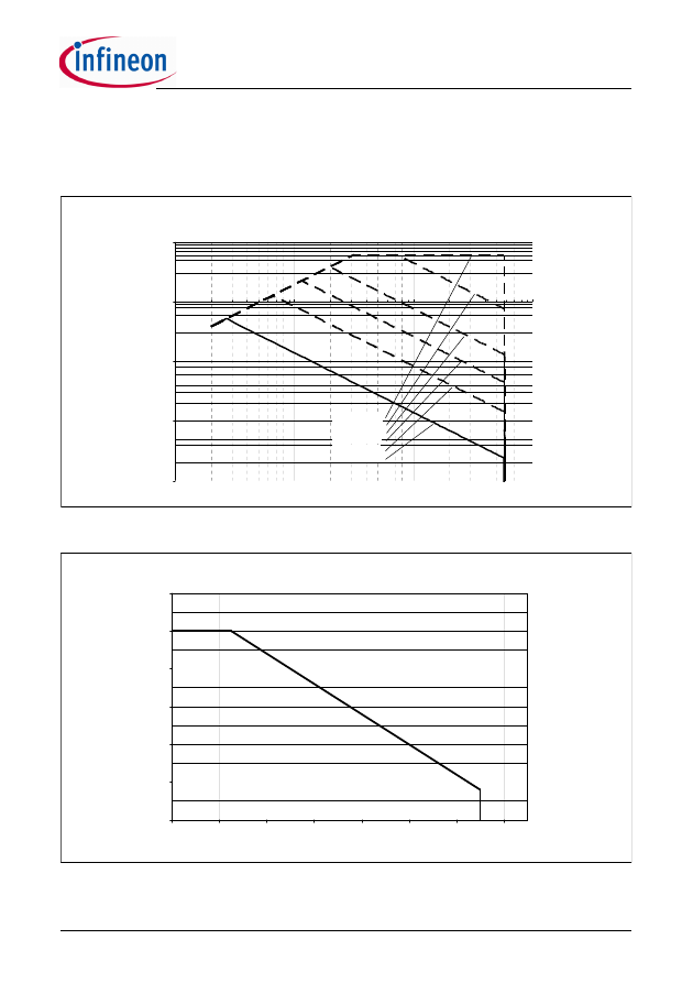
5
Typical CoolMOS
®
Performance Characteristic
Safe Operating Area for
ICE3A(B)R1765J
I
D
= f ( V
DS
)
parameter : D = 0, T
C
= 25deg.C
0.001
0.01
0.1
1
10
1
10
100
1000
V
DS
[V]
I
D
[A]
DC
tp = 100ms
tp = 0.1ms
tp = 1ms
tp = 10ms
tp = 1000ms
Figure 27
Safe Operating area (SOA) curve for ICE3BR1765J
SOA temperature derating coefficient curve
( package dissipation ) for F3 & F2 CoolSET
0
20
40
60
80
100
120
0
20
40
60
80
100
120
140
Ambient/Case temperature Ta/Tc [deg.C]
Ta : DIP, Tc : TO220
SOA tem
per
atur
e der
ati
ng coeffi
ci
ent [%]
Figure 28
SOA temperature derating coefficient curve
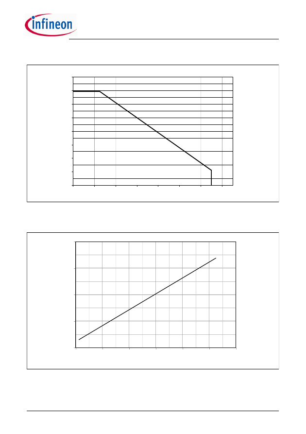
Allowable Power Dissipation for F3 CoolSET in DIP-8 package
0.0
0.2
0.4
0.6
0.8
1.0
1.2
1.4
1.6
0
20
40
60
80
100
120
140
Ambient temperature, T
a
[deg.C]
Allowable Power
Dissipat
ion,
P
tot
[W]
CoolSET
®
-F3R
ICE3BR1765J
Typical CoolMOS
®
Performance Characteristic
Version 2.3
25
19 Nov 2012
Figure 29
Power dissipation; P
tot
=f(T
a
)
540
580
620
660
700
-60
-20
20
60
100
140
180
T
j
[°C]
V
BR(DSS)
[V]
Figure 30
Drain-source breakdown voltage; V
BR(DSS)
=f(T
j
)
CoolSET
®
-F3R
ICE3BR1765J
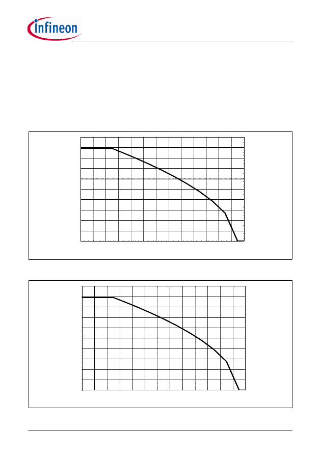
Input Power Curve
Version 2.3
26
19 Nov 2012
6
Input Power Curve
Two input power curves giving the typical input power versus ambient temperature are showed below;
Vin=85Vac~265Vac (Figure 31) and Vin=230Vac+/-15% (Figure 32). The curves are derived based on a typical
discontinuous mode flyback model which considers either 50% maximum duty ratio or 100V maximum secondary
to primary reflected voltage (higher priority). The calculation is based on no copper area as heatsink for the device.
The input power already includes the power loss at input common mode choke, bridge rectifier and the
CoolMOS.The device saturation current (I
D_Puls
@ T
j
=125°C) is also considered.
To estimate the output power of the device, it is simply multiplying the input power at a particular operating ambient
temperature with the estimated efficiency for the application. For example, a wide range input voltage (Figure 31),
operating temperature is 50°C, estimated efficiency is 85%, then the estimated output power is 26W (31W * 85%).
Ambient Temperature [°C]
Input power (85~265Vac)
[W]
P
I-
005-
ICE
3B
R1765J
_85V
ac
0
4
8
12
16
20
24
28
32
36
40
0
10
20
30
40
50
60
70
80
90
100 110 120 130
Figure 31
Input power curve Vin=85~265Vac; P
in
=f(T
a
)
Ambient Temperature [°C]
Input power (230Vac)
[W
]
P
I-
006-
ICE
3B
R1765J
_230V
ac
0
6
12
18
24
30
36
42
48
54
60
0
10
20
30
40
50
60
70
80
90
100 110 120 130
Figure 32
Input power curve Vin=230Vac+/-15%; P
in
=f(T
a
)
CoolSET
®
-F3R
ICE3BR1765J
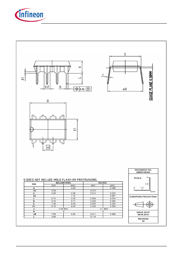
Outline Dimension
Version 2.3
27
19 Nov 2012
7
Outline Dimension
PG-DIP-8
(Plastic Dual In-Line Outline)
Figure 33
PG-DIP-8 (Pb-free lead plating Plastic Dual-in-Line Outline)
CoolSET
®
-F3R
ICE3BR1765J
Marking
Version 2.3
28
19 Nov 2012
8
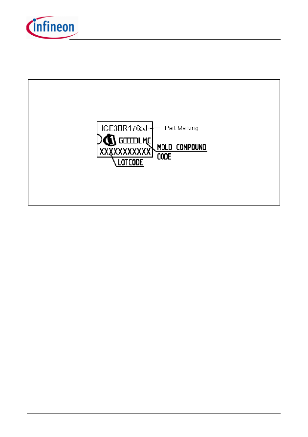
Marking
Marking
Figure 34
Marking for ICE3BR1765J
CoolSET
®
-F3R
ICE3BR1765J
Schematic for recommended PCB layout
Version 2.3
29
19 Nov 2012
9
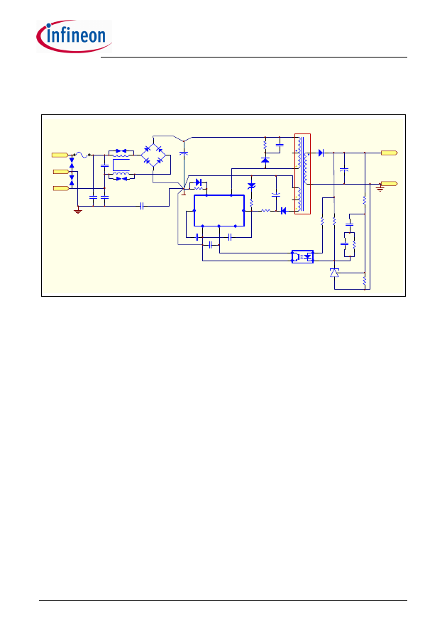
Schematic for recommended PCB layout
C11
bulk cap
R11
D11
C12
IC12
R12
C13
C16
C15
C14
D13
R14
R23
R22
IC21
C23
R24
C22
R21
R25
GND
Vo
D21
C21
F3 CoolSET schematic for recommended PCB layout
R13
Z11
TR1
N
L
BR1
C2
Y-CAP
C3
Y-CAP
C1
X-CAP
L1
FUSE1
C4
Y-CAP
GND
Spark Gap 3
Spark Gap 4
D11
Spark Gap 1
Spark Gap 2
FB
CS
GND
NC
BA
VCC
F3
DRAIN
CoolSET
IC11
*
Figure 35
Schematic for recommended PCB layout
General guideline for PCB layout design using F3/F3R CoolSET
®
(refer to Figure 35):
1. “Star Ground “at bulk capacitor ground, C11:
“Star Ground “means all primary DC grounds should be connected to the ground of bulk capacitor C11
separately in one point. It can reduce the switching noise going into the sensitive pins of the CoolSET
®
device
effectively. The primary DC grounds include the followings.
a. DC ground of the primary auxiliary winding in power transformer, TR1, and ground of C16 and Z11.
b. DC ground of the current sense resistor, R12
c. DC ground of the CoolSET
®
device, GND pin of IC11; the signal grounds from C13, C14, C15 and collector
of IC12 should be connected to the GND pin of IC11 and then “star “connect to the bulk capacitor ground.
d. DC ground from bridge rectifier, BR1
e. DC ground from the bridging Y-capacitor, C4
2. High voltage traces clearance:
High voltage traces should keep enough spacing to the nearby traces. Otherwise, arcing would incur.
a. 400V traces (positive rail of bulk capacitor C11) to nearby trace: > 2.0mm
b. 600V traces (drain voltage of CoolSET
®
IC11) to nearby trace: > 2.5mm
3. Filter capacitor close to the controller ground:
Filter capacitors, C13, C14 and C15 should be placed as close to the controller ground and the controller pin
as possible so as to reduce the switching noise coupled into the controller.
Guideline for PCB layout design when >3KV lightning surge test applied (refer to Figure 35):
1. Add spark gap
Spark gap is a pair of saw-tooth like copper plate facing each other which can discharge the accumulated
charge during surge test through the sharp point of the saw-tooth plate.
a. Spark Gap 3 and Spark Gap 4, input common mode choke, L1:
Gap separation is around 1.5mm (no safety concern)

CoolSET
®
-F3R
ICE3BR1765J
Schematic for recommended PCB layout
Version 2.3
30
19 Nov 2012
b. Spark Gap 1 and Spark Gap 2, Live / Neutral to GROUND:
These 2 Spark Gaps can be used when the lightning surge requirement is >6KV.
230Vac input voltage application, the gap separation is around 5.5mm
115Vac input voltage application, the gap separation is around 3mm
2. Add Y-capacitor (C2 and C3) in the Live and Neutral to ground even though it is a 2-pin input
3. Add negative pulse clamping diode, D11 to the Current sense resistor, R12:
The negative pulse clamping diode can reduce the negative pulse going into the CS pin of the CoolSET
®
and
reduce the abnormal behavior of the CoolSET
®
. The diode can be a fast speed diode such as IN4148.
The principle behind is to drain the high surge voltage from Live/Neutral to Ground without passing through the
sensitive components such as the primary controller, IC11.

Qualität hat für uns eine umfassende
Bedeutung. Wir wollen allen Ihren
Ansprüchen in der bestmöglichen
Weise gerecht werden. Es geht uns also
nicht nur um die Produktqualität –
unsere Anstrengungen gelten
gleichermaßen der Lieferqualität und
Logistik, dem Service und Support
sowie allen sonstigen Beratungs- und
Betreuungsleistungen.
Dazu gehört eine bestimmte
Geisteshaltung unserer Mitarbeiter.
Total Quality im Denken und Handeln
gegenüber Kollegen, Lieferanten und
Ihnen, unserem Kunden. Unsere
Leitlinie ist jede Aufgabe mit „Null
Fehlern“ zu lösen – in offener
Sichtweise auch über den eigenen
Arbeitsplatz hinaus – und uns ständig
zu verbessern.
Unternehmensweit orientieren wir uns
dabei auch an „top“ (Time Optimized
Processes), um Ihnen durch größere
Schnelligkeit den entscheidenden
Wettbewerbsvorsprung zu verschaffen.
Geben Sie uns die Chance, hohe
Leistung durch umfassende Qualität zu
beweisen.
Wir werden Sie überzeugen.
Quality takes on an allencompassing
significance at Semiconductor Group.
For us it means living up to each and
every one of your demands in the best
possible way. So we are not only
concerned with product quality. We
direct our efforts equally at quality of
supply and logistics, service and
support, as well as all the other ways in
which we advise and attend to you.
Part of this is the very special attitude of
our staff. Total Quality in thought and
deed, towards co-workers, suppliers
and you, our customer. Our guideline is
“do everything with zero defects”, in an
open manner that is demonstrated
beyond your immediate workplace, and
to constantly improve.
Throughout the corporation we also
think in terms of Time Optimized
Processes (top), greater speed on our
part to give you that decisive
competitive edge.
Give us the chance to prove the best of
performance through the best of quality
– you will be convinced.
h t t p : / / w w w . i n f i n e o n . c o m
Total Quality Management
Published by Infineon Technologies AG
Document Outline
- 1 Pin Configuration and Functionality
- 2 Representative Blockdiagram
- 3 Functional Description
- 4 Electrical Characteristics
- 5 Typical CoolMOS® Performance Characteristic
- 6 Input Power Curve
- 7 Outline Dimension
- 8 Marking
- 9 Schematic for recommended PCB layout
Wyszukiwarka
Podobne podstrony:
G2 PW S DS Rys 03 05
G2 PW S DS Rys 03 03
G2 PW T DS Rys 03
G2 PW S DS Rys 03 07
G2 PW S DS Rys 03 05
99920 1979 03 EN 2 16
99920 1979 03 EN 2 11
99920 1979 03 EN 2 07
99920 1979 03 EN 2 03
wfhss guideline 03 en
99920 1979 03 EN 2 13
G2 PW T DS Rys 03
99920 1979 03 EN 2 05
G2 PW S DS Rys 03 05
G2 PW S DS Rys 03 07
99920 1979 03 EN 2 15
99920 1979 03 EN 2 12
99920 1979 03 EN 2 14
99920 1979 03 EN 2 04
więcej podobnych podstron