THAT Corporation; 45 Sumner Street; Milford, Massachusetts 01757-1656; USA
Tel: +1 (508) 478-9200; Fax: +1 (508) 478-0990; Web: www.thatcorp.com
A Low Parts Count, Two-Slope Compressor
Abstract
Compressing the dynamic range of an audio
signal can be of significant benefit in certain play-
back applications. In multimedia sound systems,
for example, compressing the subwoofer signal
can lend added richness to the sound, particu-
larly at lower signal levels.
With automotive
sound systems, compression can raise low-level
signals above the relatively high ambient noise
level.
Speaker protection is also important, and a
dynamic range limiter is an essential component
of any system that attempts to handle overloads
gracefully (inaudibly).
This paper describes a combination compres-
sor and limiter, with adjustable threshold and
compression ratio, for just these types of applica-
tions. The basic circuit is built around a single
integrated circuit, the THAT 4311, a low-power,
low-voltage Analog Engine
Ò
IC. The THAT 4311
(like its higher-performance, higher-power cousin,
the THAT 4301) provides a high-quality voltage
controlled amplifier (VCA) and RMS-level detector
with three general purpose op amps. Using either
the THAT 4311 or THAT 4301, the dual-slope
compressor provides a very useful functional
block at reasonable cost and reduced board
space.
T H A T
C o r p o r a t i o n
APPLICATION NOTE 105
A Low Parts Count, Two-Slope Compressor
Introduction
Dynamic range compressors are one of the
most common signal processors used in the de-
velopment and reproduction of audio.
Their
ubiquity is due, in large part, to the wide variety
of applications to which they may be put. They
may be employed, for example, as automatic gain
controls, as noise reduction systems, as "effects",
as loudspeaker protection systems, or as
over-modulation limiters.
Most commercially available compressors
have a fixed or adjustable threshold, below which
no compression occurs. Above the threshold, in-
creases in signal level are reduced by a fixed or
adjustable amount, usually expressed as a ratio
of the change in signal level at the output of the
device (in decibels) over the change in signal level
at the device's input. A 6dB signal increase at the
input of 2:1 compressor, for example, would re-
sult in a 3dB increase at the compressor's output.
The compressor/limiter circuit presented in
this application note is primarily intended for use
in consumer playback products, and is a depar-
ture from the normal "above threshold" compres-
sors described above.
In particular, the
compressor/limiter described herein is a "below
threshold" compressor combined with an "above
threshold" limiter, with the transfer characteris-
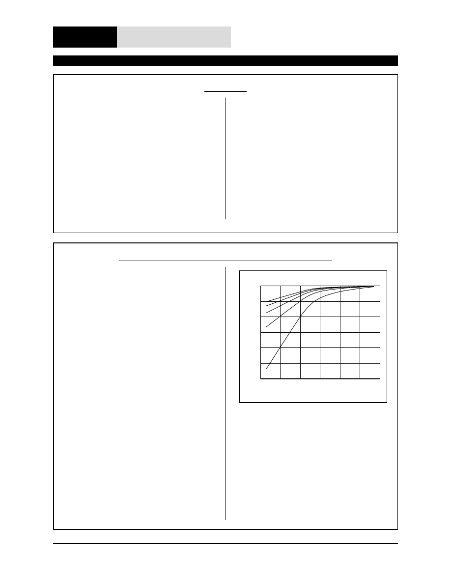
tics shown in Figure 1.
This type of device can be extremely useful in
certain applications. In automotive sound sys-
tems, for example, a constant amount of com-
pression will help overcome the high ambient
noise levels often found in the passenger com-
partment. In another application, the subwoofers
associated with multimedia speaker systems can
-30
-20
-10
0
10
20
30
dB in
-30
-25
-20
-15
-10
-5
0
dB
out
3:1
2.5:1
2:1
1.5:1
1:1 (Compression Ratio)
Figure 1. Two-slope compressor transfer characteristics
be made to sound fuller, particularly at low signal
levels, when they are fed with a compressed
low-frequency signal.
In either case, the speaker drivers need to be pro-
tected from overload, preferably in an inaudible man-
ner. One protection method uses diode clippers to
limit signal excursion. This technique alone, how-
ever, will sound particularly bad so long as the signal
remains above the clipping threshold.
Another technique uses a peak limiter to quickly
reduce the signal level. A common objection to this
method, however, is that peak limiters tend to react
to otherwise inaudible "peaks of short duration", re-
sulting in an audible artifact that has been described
as "punching a hole in the audio".
A less audible technique that better maintains
headroom while limiting harmful signal excursion
combines an RMS-based limiter with a diode clipper.
During peaks of short duration, the diodes clip the
signal. However, because the overload lasts only a few
cycles, the clipping action remains inaudible. Should
the signal remain in the overload region long enough,
however, the RMS-based limiter will act to bring the
signal level into the normal operating regime.
The combination of compressor and limiter, built
around a single VCA and RMS-level detector, deliver
significant and audible benefits to multimedia, auto-
motive, and other types of sound systems. It is this
combination of constant, below threshold compres-
sion, and effective, inaudible limiting protection that
is presented in the sections that follow.
The Feedforward Compressor
The basic feedforward compressor topology is
shown in Figure 1. The gain in dB of block G is set
by way of a control path through the block marked
b
.
If we analyze this circuit in the log domain, we
can see by inspection that,
dB
= dB
G
out
in
dB
+
The control path equation is given by,
G
x dB
dB
in
= - b
where beta is the control constant. Note that the neg-
ative sign is required for compressor action. Note,
too, that the gain (G
dB
) becomes negative (in dB) as
the input goes above 0dB, and is positive when the
signal is below 0dB.
Combining these equations results in:
dB
dB
dB
out
in
in
=
-
´ b
This equation can be rearranged to yield
( )
dBin
dBout
=
-
1
1
b
which is the compression ratio. Thus, if
b
is one,
then the compression ratio will be infinite, and if
b
is
zero, the compression ratio will be one.
If
b
is
one-half, the compression ratio will be 2:1.
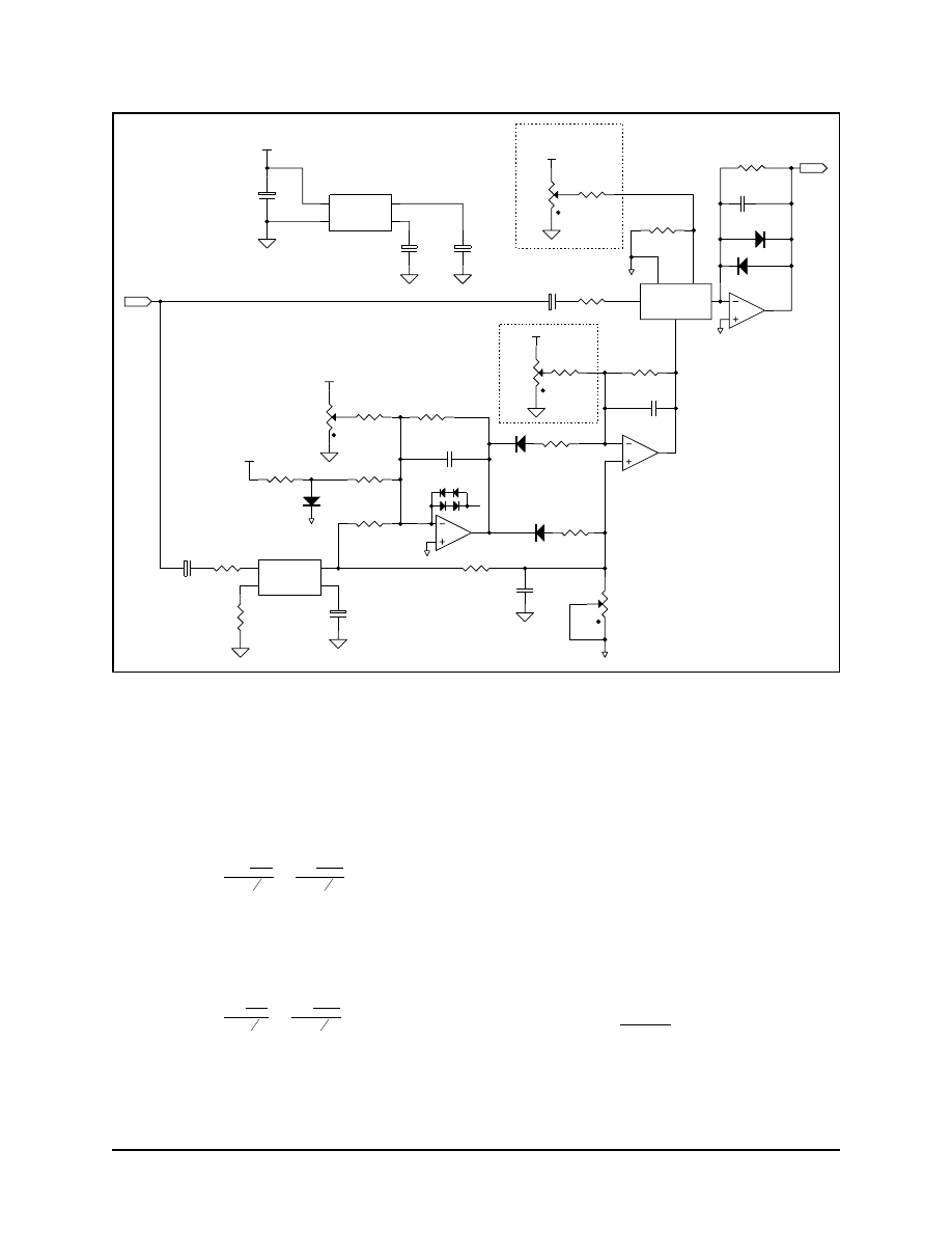
Theory of Operation
The circuit shown in Figure 3, based on the
THAT4311, implements a compressor that com-
presses below threshold and limits above threshold.
This circuit is, in many regards, similar to other
feedforward compressor/limiters, and the equations
derived in the section above apply to its operation.
Below-threshold limiting is accomplished by feed-
ing a portion of the RMS detector’s output through
the non-inverting input of the control port buffer
(U1D).
The below-threshold side-chain gain is a
function of the setting of VR1, and results in a com-
pression ration that varies between 1:1 and approxi-
mately 3:1.
Above-threshold limiting results from driving the
VCA’s Ec- control port from the output of the thresh-
old amplifier (U1C) through the inverting input of the
control port buffer (U1D) for a net side-chain gain of
one. This action results in infinite compression. A
THAT Corporation; 45 Sumner Street; Milford, Massachusetts 01757-1656; USA
Tel: +1 (508) 478-9200; Fax: +1 (508) 478-0990; Web: www.thatcorp.com
Page 2
Application Note 105
A Low Parts Count, Two-Slope Compressor
dBin
G
dBout
-
b
Figure 2: Basic feedforward compressor topology

portion of the threshold amplifier output (which is
inverted) is fed into the below-threshold compression
path which effectively cancels the below-threshold
signal, and keeps its setting from affecting the ulti-
mate above-threshold compression ratio. This ar-
rangement allows the circuit to compress when the
input is below threshold and limit when the input is
above threshold, without the below-threshold adjust-
ment affecting the ratio required for effective limiting.
RMS Detector
THAT Corporation’s RMS-level detectors exhibit
true-rms response, have greater than 80 dB of dy-
namic range, and can handle signals with crest fac-
tors greater than 8. The input of these detectors is
the virtual ground (biased at V
REF
) of an internal
op-amp, and it is at this point that the input voltage
is converted to a current. This current is full-wave
rectified and fed through a series pair of di-
ode-connected transistors.
Drawing the current
through the diode-connected transistors logs and
doubles the signal (Note that doubling the signal in
the log domain is equivalent to squaring the signal in
the linear domain). The signal is then averaged by a
log domain filter consisting of an internal diode bi-
ased by I
Time
and an external capacitor, C
T
(C3). This
circuit performs the “mean” portion of the calcula-
tion. The square root portion of the RMS calculation
is performed implicitly at the exponential control
port of the VCA.
Logging, squaring and rectification of the input
current results in the accumulation of several diode
drops on the signal, one of which is removed by the
diode-connected transistor in the log filter. The addi-
tional diode drops are removed by “bucking them
out” with diodes biased by a fixed current, which in
the case of the THAT 4311, is a replica of the timing
current that is reflected to the log filter. When the
current through the log filter diode and the “bucking”
diodes equals the RMS detector’s input current, the
offsets will cancel exactly, and the output of the detec-
tor will be at V
REF
. This point is referred to as the
0dB reference level.
If we program
I
.
A
T
=
7 5
m
then the current reflected to the “IT” pin will be
I
.
A
time
=
7 5
m
This also sets the 0dB reference current at:
I
.
A
dB
0
7 5
=
m
We can calculate the appropriate timing resistor
to be
R
k
T
V
I
V
. A
ref
T
=
=
»
2
7 5
264
m
W
The desired 0dB reference level for this circuit is
-10 dBu or 245 mV
RMS
. Knowing both this and the
0dB reference current, we can calculate the required
input resistance which is
R
. k
IN
V
I
mV
. mA
dB
dB
RMS
=
=
»
0
0
245
7 5
324
W
Since the rectified signal has already been logged
by the time the “mean” portion of the RMS calcula-
tion is performed, these detectors use a log filter for
averaging. This filter consists of an internal diode,
biased by I
time
, and an external timing capacitor, C
T
.
The time constant can be calculated as,
t =
V
I
T
T
time
C
If we choose 16 ms (which is a compromise be-
tween the best time constants for a compressor and a
limiter, the tradeoff being greater ripple--induced dis-
tortion for faster response time) as
t
, then we can
calculate C
T
:
C
. F
T
I
V
time
T
=
»
t
m
4 7
These values are reflected in Figure 3. If a single
t
for both compression AND limiting is unacceptable,
the designer should consider the “non-linear capaci-
tor”, which is discussed in detail at the end of THAT
Corporation’s Application Note AN103, Signal Lim-
iter for Power Amplifiers.
The Threshold Amplifier
The circuit immediately surrounding U1C is a
soft-knee threshold amplifier. This portion of the cir-
cuit is fundamentally an inverting amplifier with an
output offset adjustment which acts to set the thresh-
old, and a fixed offset, generated by D3, to “buck out”
the forward drops of D1 and D2 in the control port
buffer. D1 and D2 in the control port buffer cause
the circuit to work only above threshold.
THAT Corporation; 45 Sumner Street; Milford, Massachusetts 01757-1656; USA
Tel: +1 (508) 478-9200; Fax: +1 (508) 478-0990; Web: www.thatcorp.com
Rev. 10/6/00
Page 3

The gain for the RMS detector output signal
through the threshold amplifier is
A
40.2 k
10 k
n =
»
-
W
W
4
which results in a control voltage constant at the out-
put of the threshold amplifier of
k
.
.
CV
mV
dB
mV
dB
=
´
=
4
61
24 4
The voltage across D3 (biased by R14) is ampli-
fied by -1, and effectively cancels the offsets of D1
and D2. Thus, neglecting the effect of the threshold
adjustment, when the RMS detector output goes
above zero volts, D1 and D2 will begin to conduct,
and the signal will be above threshold. 75 k
W
was
chosen as the value for R14 since this value resulted
in a current that best compensated for ambient tem-
perature variations and the current variations in D2
that result from changes in the setting of VR1.
VR2 and R23 provide a means to adjust the level
where this action occurs. When VR2 is set fully
clockwise (CW), the threshold offset is:
Adj
threshold
V
V
R
R
mV
dB
k
=
é
ë
ê
ù
û
ú =
-
´
-
´
-
-
2
24 4
2
10
23
40 2
.
.
W
165
24 4
20
k
mV
dB
dB
W
.
»
In this case, the ultimate sign of the result is a
consequence of the voltage polarity, inverting gains of
both the threshold amplifier and the control port
buffer, and the control port polarity. Since this is rel-
ative to the RMS detector’s 0dB reference level, which
is -10 dBu, a fully CW VR2 results in a threshold of
10 dBu.
When VR2 is set fully counter-clockwise (CCW),
the threshold offset is
Adj
threshold
V
V
R
R
mV
dB
k
=
é
ë
ê
ù
û
ú =
´
´
-
-
3
24 4
3
10
23
40 2
16
.
.
W
5
24 4
30
k
mV
dB
dB
W
.
» -
Again, this result is relative to the RMS detector’s
0dB reference level, which is -10 dBu, and as a re-
sult, a fully CCW VR2 results in a threshold of
-40dBu.
The Control Port Buffer
The control port of the VCA is driven by U1D,
which acts as the control port buffer. Buffering is not
strictly required, since the control port can be driven
by a resistive divider with a non-inductive impedance
of less than 51
W
without substantially increasing its
THD+N. Unfortunately, the control voltage required
to achieve 65 dB of attenuation across 51
W
requires
greater than 6 mA of drive current, which is roughly
equal to the quiescent current of the THAT4311, and
in any case, cannot be handled by the on-chip refer-
ence. (This situation is also unacceptable for battery
powered applications, and is generally bad practice).
For this reason, an op-amp is typically used to drive
the control port.
The signal fed to the control port buffer comes
from two sources: the threshold amplifier and di-
rectly from the RMS detector. While the input signal
is below threshold, an attenuated portion of the RMS
output is fed into the non-inverting input of OA1. At
this point in the circuit’s operation, D1 and D2 are
reverse biased, and the non-inverting gain of OA1 is
essentially one. The side chain gain, which deter-
mines the compression ratio, is purely a function of
R7 and the position of VR1.
We can see intuitively that when VR1 is fully coun-
ter-clockwise, the side chain gain is zero, and the
compression ratio can be calculated as,
C R
VR eff
R
VR eff
k
. .
:
=
=
=
-
-
+
+
1
1
1
1
1
7
1
0
10
0
1 1
W
Likewise, when VR1 is fully CW,
C R
VR eff
R
VR eff
k
k
k
. .
:
=
=
=
-
-
+
+
1
1
1
1
1
7
1
20
10
20
3 1
W
W
W
It is easily verified that when VR1 is set at 25%
CW, C.R.=1.5:1; at 50% CW, C.R.=2:1; and at 75%
CW, C.R.=2.5:1.
When the input signal goes above threshold, cur-
rent flows through D1 and D2. OA1’s inverting gain
for this signal approaches
A
OA
R
R
k
k
1
13
12
10
40 2
1
4
=
=
» -
-
-
W
W
.
and this coupled with the gain of -4 in the threshold
amplifier, results in a net gain of one through this
path. The gain through the non-inverting input of
OA1 approaches zero (when the RMS signal is well
above threshold), since the current through R11 ulti-
mately cancels that through R7. The resulting above-
threshold compression ratio is therefore
C R
. .
:
=
= ¥
-
1
1 1
1
which makes the circuit a limiter when the input is
above threshold.
THAT Corporation; 45 Sumner Street; Milford, Massachusetts 01757-1656; USA
Tel: +1 (508) 478-9200; Fax: +1 (508) 478-0990; Web: www.thatcorp.com
Page 4
Application Note 105
A Low Parts Count, Two-Slope Compressor
The control port buffer also has an optional
make-up gain adjustment which is implemented by
adding a voltage offset to the control port. The cur-
rent through R16 is summed into the side chain at
the inverting input of OA1. The amount and polarity
of the current is dependent on the setting of VR2.
When VR2 is set fully CW, the gain is
A
make up
V
V
R
R
mV
dB
k
k
-
-
´
´
= -
é
ë
ê
ù
û
ú =
-
-
2
6 1
2
6
13
16
10
165
.
.
W
W
1
20
mV
dB
dB
» -
The ultimate sign of the result is a consequence of
the voltage polarity, inverting gain, and the control
port polarity. When VR2 is set fully CCW, the gain is
A
make up
V
V
R
R
mV
dB
k
k
-
´
´
= -
é
ë
ê
ù
û
ú =
-
-
3
6 1
3
6 1
13
16
10
165
.
.
W
W
mV
dB
dB
» -
30
The VCA
The THAT 4311 incorporates a log/anti-log VCA.
These devices first log the signal, and then add an
offset to the logged signal (which is equivalent to mul-
tiplication of the un-logged signal). The signal is then
sent through a pair of anti-log diodes and into a
transimpedance amplifier (formed by OA3 and R2),
restoring the signal to the linear domain.
A more
detailed explanation of the internal workings of these
VCAs can be found in the 2150/2180/2181
datasheets.
Mismatches in the log and anti-log diodes (which
are actually transistors) produce 2nd harmonic dis-
tortion which can be as high as 0.7%, though it rarely
exceeds 0.3% in production devices. This level of
performance is often acceptable in computer speaker,
sub-woofer, and some companding applications. For
those applications where this level of performance is
unacceptable, an optional symmetry trim is shown
which can reduce the THD+N to below 0.1% at nomi-
nal input levels and gains.
An often overlooked aspect of limiter design is the
need for a clipper. While infinite compression can ul-
THAT Corporation; 45 Sumner Street; Milford, Massachusetts 01757-1656; USA
Tel: +1 (508) 478-9200; Fax: +1 (508) 478-0990; Web: www.thatcorp.com
Rev. 10/6/00
Page 5
R1
22k
R4
51R
R2
22k
R5
264k
R6
10k0
R9
40k2
R10
40k2
R7
10k0
R11
40k2
R12
40k2
R13
10k0
C1
47u
C3 (C )
T
4u7
C4
22u
C5
100n
C7
47p
VR3
20k
D1
1N4148
D2
1N4148
R14
75k
VR2
50k
Below Threshold
Compression Ratio
R18
32k4
In
Out
10dBu
-40dB
1:1
3:1
C12
100p
R23
165k
C11
100n
VR5
50k
R16
165k
Gain
Threshold
C2
10u
R3
33k
VR6
50k
24.4mV/dB
-20dB
30dB
D1
1N4148
D4
1N4148
D5
1N4148
IN
17
12
OUT
VCA
EC+
SYM
EC-
OA3
Vref
U1A
THAT 4311
Iset
2
TC
5
IN
1
OUT
4
RMS
U1B
THAT 4311
3
7
OA2
Vref
6
U1C
THAT4311
18
19
20
OA1
U1D
THAT 4311
Cap
8
Vee
10
Vref 9
Vcc
11
Vref
U1E
THAT 4311
C8
10u
C6
22u
+5
Vref
Vref
Vref
+5
+5
+5
+5
Vin0=-10dBu
Optional
Make-up
Symmetry
Trim
Optional
15
16
14
13
+
+
+
+
+
+
Figure 3: Multi-slope Compressor / Limiter

timately bring the output signal below overdrive lev-
els, the level detector has a finite response time, and
during this time, subsequent devices in the signal
chain which have poor overload characteristics can
produce audible artifacts. This circuit uses a pair of
1N4148 diodes to implement a clipper, though there
are other, more versatile solutions such as the ad-
justable, transistor-based clipper shown in Figure 2
of the aforementioned Application Note AN103.
The gain cell in the THAT 4311 is current source
biased, and there is approximately 500
m
A available
to handle signal currents. The polarity of the VCA’s
input and output signals is the same, so the total of
the peak input and output currents cannot exceed the
available bias current, or the VCA will clip internally.
The clipping diodes in the feedback loop of OA3
limit the output swing to ±0.6V, and if the limiter is
adjusted properly, we can calculate the maximum
VCA output current
I
A
OUT Max
V
R
V
k
Out
Peak
=
´
=
2
0 6
22
27
.
W
m
This leaves approximately 475
m
A available for in-
put signal current. Therefore, the maximum input
voltage would be
V
k
A
V
In Max Peak
Peak
=
´
=
22
475
10 45
W
m
.
which is 7.4 V
RMS
, or about 20 dBu.
Reference Considerations
The THAT 4311 has an on-chip, 2V reference
about which the VCA, the RMS detector, and OA2 are
internally biased. Pins are provided for filter capaci-
tors at both the input and the output of the buffer,
which are labeled CAP and VREF respectively. Setting
C6=22mF and C8=10mF has proven to be effective
at minimizing reference noise, and little is gained by
making the values larger.
Conclusion
The THAT 4311 and its cousin, the THAT 4301,
provide ideal, single chip solutions to many dynamics
signal processing problems. The circuit discussed
above implements a combination above-threshold
limiter and below-threshold compressor. The low
power consumption of the THAT 4311 make it suit-
able for battery-powered applications such as “stomp
boxes” and “boom boxes”.
THAT Corporation; 45 Sumner Street; Milford, Massachusetts 01757-1656; USA
Tel: +1 (508) 478-9200; Fax: +1 (508) 478-0990; Web: www.thatcorp.com
Page 6
Application Note 105
A Low Parts Count, Two-Slope Compressor
Wyszukiwarka
Podobne podstrony:
Stitch Odd Count Two Bead Peyote
The Splashpower technology comprises two parts
Two low temperature Stirling engines, WSZYSTKO O ENERGII I ENERGETYCE, SILNIK STIRLINGA, WIADMOŚCI
Two Drop Odd Count Peyote
William Tenn Party of the Two Parts
Party of the Two Parts William Tenn(1)
Okidata Okipage 14e Parts Manual
Biochemia TZ wyklad 12 integracja metabolizmu low
Kyocera FS 1010 Parts Manual
All Flesh Must Be Eaten Two Rotted Thumbs Up
Brother PT 2450 Parts Manual
cs175 176 compressed
Brit M Two Men and a Lady Prequel [Ravenous] (pdf)
ŚPIEWNIK HARCERSKI 2 compressed(4)
A10VO Series 31 Size 28 Service Parts list
Akumulator do AMA COMPRESSOR ST180H 1 2
Comprendre
Micele na?lowniku
In literary studies literary translation is a term of two meanings rev ag
więcej podobnych podstron