CAT3626
© Catalyst Semiconductor, Inc.
1
Doc. No. MD-5014 Rev. C
Characteristics subject to change without notice
6-Channel LED Driver with I
2
C™ Interface
FEATURES
Drives 6 LED channels
Independent current on 3 pairs of LEDs
I
2
C serial interface programming
Adjustable current to 32mA in 0.5mA step
Power efficiency up to 91%
Fractional pump 1x/1.5x
Low noise input ripple
Fixed High Frequency Operation 1MHz
“Zero” Current Shutdown Mode
Soft start and current limiting
Short circuit protection
Thermal shutdown protection
APPLICATIONS
RGB LEDs
LCD and keypad Backlighting
Cellular Phones, PDAs
Digital Cameras
ORDERING INFORMATION
Part Number
Package
Quantity
per Reel
Package
Marking
CAT3626HV4-T2 TQFN-16
(1)
2000 G626
CAT3626HV4-GT2 TQFN-16
(2)
2000 CDAJ
Notes: (1) Matte-Tin Plated Finish (RoHS-compliant)
(2) NiPdAu Plated Finish (RoHS-compliant)
PRODUCT DESCRIPTION
The CAT3626 is a high efficiency 1x/1.5x fractional
charge pump with programmable dimming current in
six LED channels. To ensure uniform brightness in
LCD backlight applications, each LED channel delivers
an accurate regulated current.
Low noise and input ripple is achieved by operating at
a constant switching frequency of 1MHz which allows
the use of small external ceramic capacitors. The
1x/1.5x fractional charge pump supports a wide range
of input voltages from 3V to 5.5V with efficiency up to
91%, and is ideal for Li-Ion battery powered devices.
The LED channels are configured into three indepen-
dent pairs, each containing 2 matched channels. Each
pair can be separately programmed from zero to 32mA,
in 0.5mA resolution steps, using the I
2
C serial interface.
Any individual channel can be disabled while others
remain active. When the enable input (EN) is low, the
device is in shutdown mode drawing zero current.
The device is available in a 16-pad thin QFN package
with a max height of 0.8mm.
For Ordering Information details, see page 14.
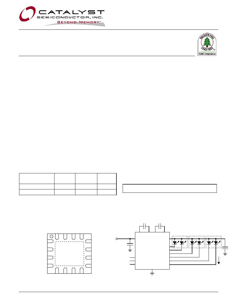
PIN CONFIGURATION
TYPICAL APPLICATION CIRCUIT
TQFN 16-pad 4 x 4mm
(Top View)
I
2
C is a trademark of Philips Corporation. Catalyst Semiconductor is licensed by Philips Corporation to carry the I
2
C bus protocol.
16
15
14
13
12
11
10
9
1
2
3
4
5
6
7
8
LEDA1
SDA
SCL
EN
LEDC2
GND
C2+
C2-
LEDA2 LEDB1 LEDB2 LEDC1
VOUT
VIN
C1-
C1+
GND
V
IN
3V to
5.5V
LEDA1
LEDA2
LEDB1
LEDB2
LEDC1
LEDC2
EN
CAT3626
VIN
VOUT
1µF
1µF
C
IN
C1+
C1-
C2+
C2-
SDA
SCL
1µF
1µF
20mA
pair A
pair B
pair C
C
OUT
ENABLE
I
2
C Interface
CAT3626
Doc. No. MD-5014 Rev. C
2
© Catalyst Semiconductor, Inc.
Characteristics subject to change without notice
ABSOLUTE MAXIMUM RATINGS
Parameters Ratings
Units
VIN, LEDxx voltage
6
V
VOUT, C1±, C2± voltage
7
V
EN, SDA, SCL voltage
VIN + 0.7V
V
Storage Temperature Range
-65 to +160
ºC
Junction Temperature Range
-40 to +150
ºC
Lead Temperature
300
ºC
RECOMMENDED OPERATING CONDITIONS
Parameter Range
Units
VIN
3 to 5.5
V
Ambient Temperature Range
-40 to +85
ºC
LED forward voltage
Up to 4.2
V
I
LED
per LED pin
0 to 32
mA
Typical application circuit with external components is shown on page 1.
ELECTRICAL OPERATING CHARACTERISTICS
V
IN
= 3.6V, EN = High, ambient temperature of 25ºC (over recommended operating conditions unless specified
otherwise)
Symbol Parameter
Test
Conditions
Min
Typ
Max
Units
I
Q
Quiescent
Current
1x mode, all LEDs Off
1x mode, all LEDs On
1.5x mode, all LEDs Off
0.5
2.2
3.5
mA
mA
mA
I
QSHDN
Shutdown
Current
V
EN
= 0V
0
1
µA
I
LED
LED Current Range with 6 LEDs
0
32
mA
I
LED-ACC
LED Current Accuracy
1mA ≤ I
LED
≤ 31mA
±3
%
I
LED-DEV
LED Channel Matching
(I
LED
- I
LEDAVG
) / I
LEDAVG
±3
%
R
OUT
Output Resistance (open loop)
1x mode, I
OUT
= 120mA
1.5x mode, I
OUT
= 120mA
0.5
2.8
Ω
Ω
F
OSC
Charge Pump Frequency
0.8
1
1.3
MHz
I
SC_MAX
Output short circuit Current Limit V
OUT
< 0.5V
60
mA
I
IN_MAX
Input Current Limit
1x mode, V
OUT
> 1V
300
mA
I
EN
V
HI-EN
V
LO-EN
EN Pin
- Input Leakage
- Logic High Level
- Logic Low Level
-1
1.3
1
0.4
µA
V
V
V
HI
V
LO
I
2
C SDA, SCL
- High Level Input Voltage
- Low Level Input Voltage
0.7 x V
IN
0.3 x V
IN
V
V
T
SD
Thermal
Shutdown
165 ºC
T
HYS
Thermal
Hysteresis
20 ºC
V
UVLO
Under-voltage lock out (UVLO)
threshold
2
V
CAT3626
© Catalyst Semiconductor, Inc.
3
Doc. No. MD-5014 Rev. C
Characteristics subject to change without notice
A.C. CHARACTERISTICS
For 3V ≤ V
IN
≤ 5.5V, over full ambient temperature range -40 to +125°C (over recommended operating conditions
unless specified otherwise).
Symbol Parameter
Min
Typ
Max
Unit
f
SCL
Clock
Frequency
400
kHz
t
AA
SCL Low to SDA Data Out and ACK Out
0.9
µs
t
BUF
Bus Free Time Before a New Transmission Can Start
1.2
µs
t
HD:STA
Start Condition Hold Time
0.6
µs
t
LOW
Clock Low Period
1.2
µs
t
HIGH
Clock
High
Period
0.6
µs
t
SU:STA
Start Condition Setup Time (For a Repeated Condition)
0.6
µs
t
HD:DAT
Data In Hold Time
0
ns
t
SU:DAT
Data In Setup Time
100
ns
t
R
SDA and SCL Rise Time
0.3
µs
t
F
SDA and SCL Fall Time
300
ns
t
SU:STO
Stop Condition Setup Time
0.6
µs
t
DH
Data Out Hold Time
50
ns
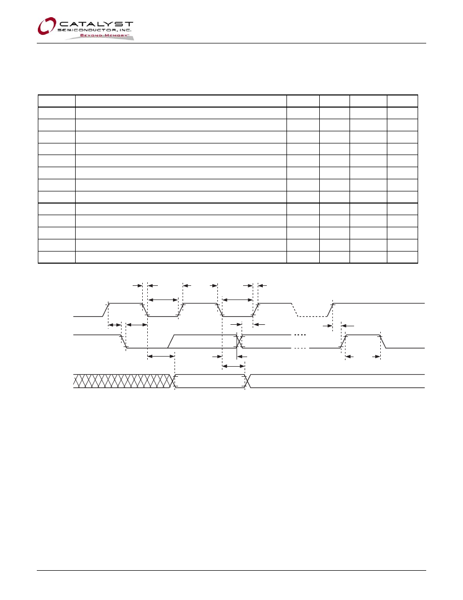
Figure 1. I
2
C Bus Timing Characteristics
t
HIGH
SCL
SDA IN
SDA OUT
t
LOW
t
LOW
t
BUF
t
SU:STO
t
SU:DAT
t
HD:DAT
t
HD:SDA
t
SU:STA
t
F
t
R
t
AA
t
DH
CAT3626
Doc. No. MD-5014 Rev. C
4
© Catalyst Semiconductor, Inc.
Characteristics subject to change without notice
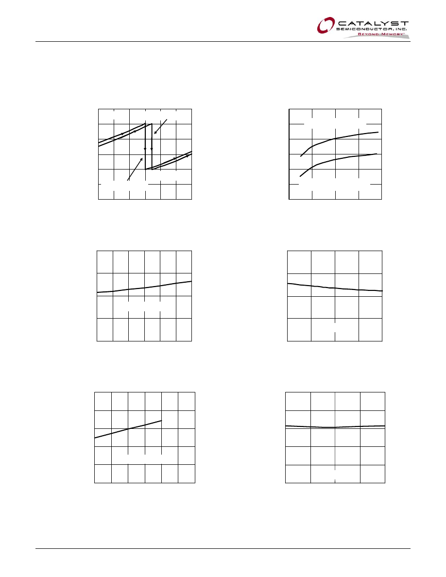
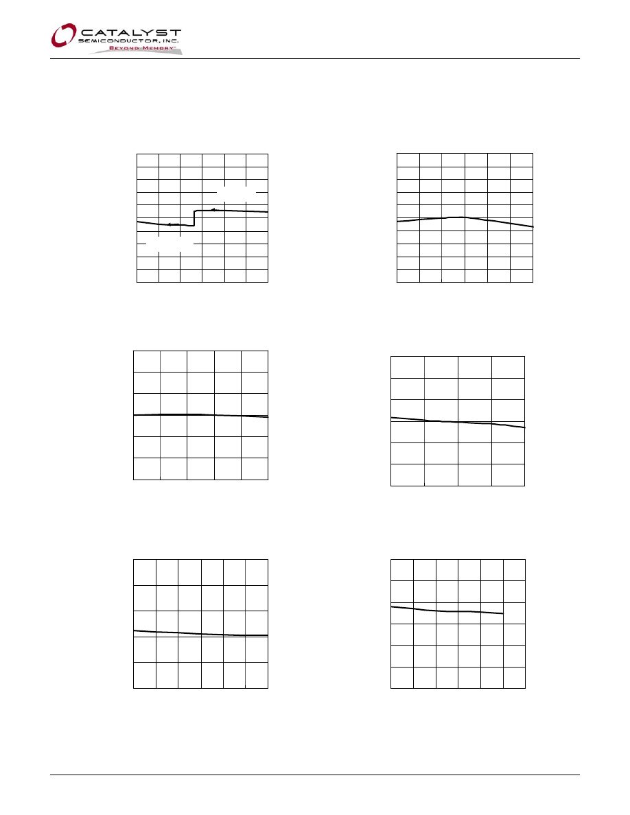
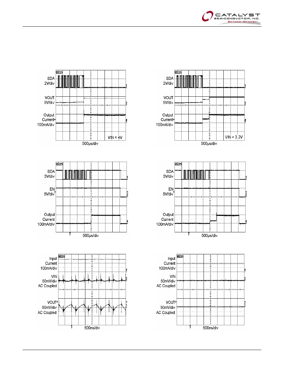
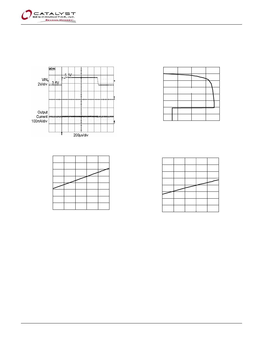
TYPICAL CHARACTERISTICS
V
IN
= 3.6V, I
OUT
= 90mA (6 LEDs at 15mA), EN = V
IN
, C
IN
= C
1
= C
2
= C
OUT
= 1µF, T
AMB
= 25ºC, unless otherwise specified.
Efficiency vs. Supply Voltage (6 LEDs)
40
50
60
70
80
90
100
3.0
3.2
3.4
3.6
3.8
4.0
4.2
SUPPLY VOLTAGE [V]
E
FFI
C
IE
N
C
Y
[
%
]
1x Mode
1.5x Mode
20mA per LED
15mA per LED
Efficiency vs. Total LED Current (6 LEDs)
40
50
60
70
80
90
100
0
50
100
150
200
TOTAL LED CURRENT [mA]
E
F
F
ICI
E
NCY
[
%
]
VIN = 4V (1x mode)
VIN = 3.2V (1.5x mode)
Quiescent Current vs. Supply Voltage (1x Mode)
0
0.2
0.4
0.6
0.8
3.0 3.2 3.4 3.6 3.8 4.0 4.2
SUPPLY VOLTAGE [V]
Q
U
IE
SC
EN
T
C
U
R
R
E
N
T
[
m
A]
6 LEDs OFF
Quiescent Current vs. Temperature (1x Mode)
0.0
0.2
0.4
0.6
0.8
-40
0
40
80
120
TEMPERATURE [°C]
Q
UI
E
S
CE
NT
CURRE
NT
[
m
A
].
6 LEDs OFF
Quiescent Current vs. Supply Voltage (1.5x Mode)
0
1
2
3
4
5
3.0
3.2
3.4
3.6
3.8
4.0
4.2
SUPPLY VOLTAGE [V]
Q
U
IESC
EN
T
C
U
R
R
E
N
T
[m
A].
6 LEDs OFF
Quiescent Current vs. Temperature (1.5x Mode)
0
1
2
3
4
5
-40
0
40
80
120
TEMPERATURE [°C]
Q
UI
E
S
CE
N
T
CU
RRE
NT
[
m
A
].
6 LEDs OFF
CAT3626
© Catalyst Semiconductor, Inc.
5
Doc. No. MD-5014 Rev. C
Characteristics subject to change without notice
TYPICAL CHARACTERISTICS
V
IN
= 3.6V, I
OUT
= 90mA (6 LEDs at 15mA), EN = V
IN
, C
IN
= C
1
= C
2
= C
OUT
= 1µF, T
AMB
= 25ºC, unless otherwise specified.
LED Current Change vs. Supply Voltage
-5.0
-4.0
-3.0
-2.0
-1.0
0.0
1.0
2.0
3.0
4.0
5.0
3.0 3.2 3.4 3.6 3.8 4.0 4.2
SUPPLY VOLTAGE [V]
LE
D
CU
RRE
NT
C
HA
NG
E
[
%
]
1x Mode
1.5x Mode
LED Current Change vs. Temperature
-5.0
-4.0
-3.0
-2.0
-1.0
0.0
1.0
2.0
3.0
4.0
5.0
-40 -20
0
20
40
60
80
TEMPERATURE [°C]
LE
D CURRE
NT
CHA
NG
E
[
%
]
Switching Frequency vs. Supply Voltage
0.7
0.8
0.9
1.0
1.1
1.2
1.3
3.0
3.2
3.4
3.6
3.8
4.0
SUPPLY VOLTAGE [V]
S
W
IT
CHI
NG
F
RE
Q
UE
NCY
[
M
Hz
]
Switching Frequency vs. Temperature
0.7
0.8
0.9
1.0
1.1
1.2
1.3
-40
0
40
80
120
TEMPERATURE [°C]
S
W
IT
CHI
NG
F
R
E
Q
UE
NC
Y
[
M
H
z]
Output Resistance vs. Supply Voltage (1x Mode)
0.0
0.2
0.4
0.6
0.8
1.0
3.0 3.2 3.4
3.6 3.8 4.0 4.2
SUPPLY VOLTAGE [V]
O
U
T
PU
T
R
ESI
ST
AN
C
E [
Ω
]
.
Output Resistance vs. Supply Voltage(1.5x Mode)
1.0
1.5
2.0
2.5
3.0
3.5
4.0
3.0 3.2
3.4 3.6 3.8
4.0 4.2
SUPPLY VOLTAGE [V]
O
U
T
PU
T
R
ESI
ST
AN
C
E [
Ω
]
.
CAT3626
Doc. No. MD-5014 Rev. C
6
© Catalyst Semiconductor, Inc.
Characteristics subject to change without notice
TYPICAL CHARACTERISTICS
V
IN
= 3.6V, I
OUT
= 90mA (6 LEDs at 15mA), EN = V
IN
, C
IN
= C
1
= C
2
= C
OUT
= 1µF, T
AMB
= 25ºC, unless otherwise specified.
Power Up with 6 LEDs at 15mA (1x Mode)
Power Up with 6 LEDs at 15mA (1.5x Mode)
Enable Power Down (1x Mode)
Enable Power Down (1.5x Mode)
Switching Waveforms in 1.5x Mode
Operating Waveforms in 1x Mode
CAT3626
© Catalyst Semiconductor, Inc.
7
Doc. No. MD-5014 Rev. C
Characteristics subject to change without notice
TYPICAL CHARACTERISTICS
V
IN
= 3.6V, I
OUT
= 90mA (6 LEDs at 15mA), EN = V
IN
, C
IN
= C
1
= C
2
= C
OUT
= 1µF, T
AMB
= 25ºC, unless otherwise specified.
Line Transient Response in 1x mode
Foldback Current Limit
0.0
0.5
1.0
1.5
2.0
2.5
3.0
3.5
4.0
0
100
200
300
400
OUTPUT CURRENT [mA]
O
U
T
PU
T
VO
LT
AG
E
[V
]
1x Mode
SDA, SCL V
IH
vs. Supply Voltage
0.0
0.5
1.0
1.5
2.0
2.5
3.0
3.5
4.0
3.0
3.5
4.0
4.5
5.0
5.5
SUPPLY VOLTAGE [V]
V
IH
[V]
SDA, SCL V
IL
vs. Supply Voltage
0.0
0.5
1.0
1.5
2.0
2.5
3.0
3.5
4.0
3.0
3.5
4.0
4.5
5.0
5.5
SUPPLY VOLTAGE [V]
VI
L [
V]
CAT3626
Doc. No. MD-5014 Rev. C
8
© Catalyst Semiconductor, Inc.
Characteristics subject to change without notice
PIN DESCRIPTIONS
Pin #
Name
Function
1
LEDA1
Cathode terminal of LED A1
2 SDA I
2
C Serial data input/output
3 SCL I
2
C Serial clock input
4 EN
Enable
input
5
VOUT
Charge pump output connected to the LED anodes
6 VIN Supply
voltage
7
C1-
Bucket capacitor 1 terminal
8
C1+
Bucket capacitor 1 terminal
9
C2-
Bucket capacitor 2 terminal
10
C2+
Bucket capacitor 2 terminal
11 GND Ground
reference
12
LEDC2
Cathode terminal of LED C2
13
LEDC1
Cathode terminal of LED C1
14
LEDB2
Cathode terminal of LED B2
15
LEDB1
Cathode terminal of LED B1
16
LEDA2
Cathode terminal of LED A2
TAB
Connect to Ground on PCB
PIN FUNCTION
VIN
is the supply pin for the charge pump. A small 1μF
ceramic bypass capacitor is required between the VIN
pin and ground near the device. The operating input
voltage range is from 2.2V to 5.5V. Whenever the input
supply falls below the undervoltage threshold (2V), all
LEDs channels will be automatically disabled.
EN
is the enable logic input for the driver. Guaranteed
levels of logic high and logic low are set at 1.3V and
0.4V respectively. When EN is initially taken high, the
device becomes enabled and all LED currents remain
at 0mA. To place the device into zero current shutdown
mode, the EN pin must be held low.
SDA
is the I
2
C serial data line. This is a bidirectional
line allowing data to be written into and read from the
four registers in the driver. Registers RegA/B/C set the
LED current in each pair of channels, while RegEn sets
the On/Off state independently of each channel.
SCL
is the I
2
C serial clock input.
VOUT
is the charge pump output that is connected to
the LED anodes. A small 1μF ceramic bypass
capacitor is required between the VOUT pin and
ground near the device.
GND
is the ground reference for the charge pump. The
pin must be connected to the ground plane on the
PCB.
C1+, C1-
are connected to each side of the 1μF
ceramic bucket capacitor C1.
C2+, C2-
are connected to each side of the 1μF
ceramic bucket capacitor C2.
LEDxx
provide the internally regulated current to the
six LED cathodes. These pins enter a high-impedance
zero-current state whenever the device is placed in
shutdown mode. In applications using less than six
LEDs, the unused channels should be disabled
through the RegEn register.
TAB
is the exposed pad underneath the package. For
best thermal performance, the tab should be soldered
to the PCB and connected to the ground plane.
CAT3626
© Catalyst Semiconductor, Inc.
9
Doc. No. MD-5014 Rev. C
Characteristics subject to change without notice
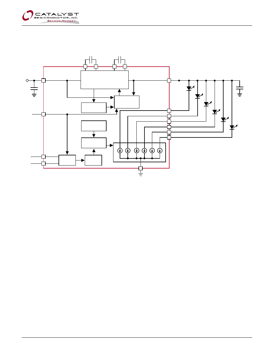
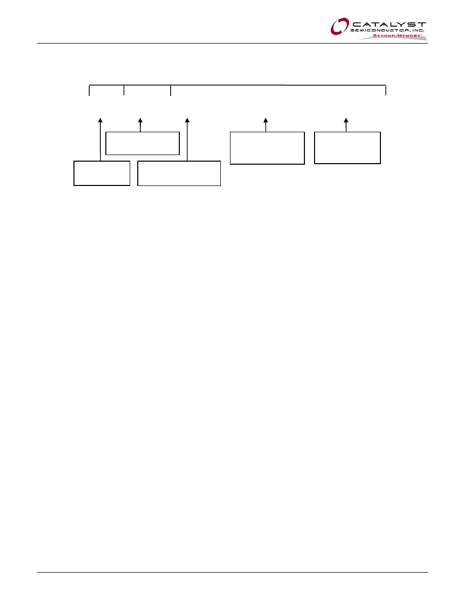
BLOCK DIAGRAM
Figure 2. CAT3626 Functional Block Diagram
BASIC OPERATION
At power-up, the CAT3626 starts operating in 1x mode
where the output will be approximately equal to the
input supply voltage (less any internal voltage losses).
If the output voltage is sufficient to regulate all LEDs
currents the device remains in 1x operating mode.
If the input voltage is insufficient or falls to a level
where the regulated currents cannot be maintained,
the device automatically switches (after a fixed time of
400µs) into 1.5x mode.
In 1.5x mode, the output is approximately equal to 1.5
times the input supply voltage (less any internal
voltage losses).
The above sequence is repeated each and every time
the chip is either powered-up or taken out of shutdown
(via EN pin), or the RegEn register is accessed by
write cycle.
LED CURRENT SETTING
The LED current setting is programmed via the I
2
C
serial interface and is stored in four
8-bit registers RegA, RegB, RegC and RegEn as
follows:
RegA stores the LED current for group A
(LEDA1 and LEDA2 channels),
RegB stores the LED current for group B
(LEDB1 and LEDB2 channels),
RegC stores the LED current for group C
(LEDC1 and LEDC2 channels),
RegEn selects the on/off state of each of the 6
LED channels.
At each write access to RegEn, the driver automatically
reconfigures to the mode (1x or 1.5x) that provides the
highest efficiency.
Mode Control
1MHz
Oscillator
Current
Setting DAC
Serial
Interface
Registers
Reference
Voltage
1x mode (LDO)
1.5x Charge Pump
V
IN
C
1-
C
2-
C
1+
C
2+
V
OUT
C
OUT
C
IN
1µF
1µF
1µF
1µF
EN
LEDA1
LEDA2
LEDB1
LEDB2
LEDC1
LEDC2
GND
6 Current
Sink Regulators
SDA
SCL
CAT3626
Doc. No. MD-5014 Rev. C
10
© Catalyst Semiconductor, Inc.
Characteristics subject to change without notice
Table 1. Register address and data configuration
Bit pattern
Register
name
Register
Address
Bit 7
Bit 6
Bit 5
Bit 4
Bit 3
Bit 2
Bit 1
Bit 0
RegA 0 X
X
RegB 1 X
X
RegC 2 X
X
See Table 2 for values
RegEn 3 X X
LEDC2
On = 1
Off = 0
LEDC1
On = 1
Off = 0
LEDB2
On = 1
Off = 0
LEDB1
On = 1
Off = 0
LEDA2
On = 1
Off = 0
LEDA1
On = 1
Off = 0
The table 2 lists the various LED currents with the associated RegA, RegB, and RegC register values.
Table 2. LED Current Selection and Register Value
(1)
LED
current
(mA)
D7
D6
D5
D4
D3
D2
D1
D0
Dec
LED
current
(mA)
D7
D6
D5
D4
D3
D2
D1
D0
Dec
0.5
X X 0 0 0 0 0 0 0
16.5
X X 1 0 0 0 0 0 32
1.0
X X 0 0 0 0 0 1 1
17.0
X X 1 0 0 0 0 1 33
1.5
X X 0 0 0 0 1 0 2
17.5
X X 1 0 0 0 1 0 34
2.0
X X 0 0 0 0 1 1 3
18.0
X X 1 0 0 0 1 1 35
2.5
X X 0 0 0 1 0 0 4
18.5
X X 1 0 0 1 0 0 36
3.0
X X 0 0 0 1 0 1 5
19.0
X X 1 0 0 1 0 1 37
3.5
X X 0 0 0 1 1 0 6
19.5
X X 1 0 0 1 1 0 38
4.0
X X 0 0 0 1 1 1 7
20.0
X X 1 0 0 1 1 1 39
4.5
X X 0 0 1 0 0 0 8
20.5
X X 1 0 1 0 0 0 40
5.0
X X 0 0 1 0 0 1 9
21.0
X X 1 0 1 0 0 1 41
5.5
X X 0 0 1 0 1 0 10
21.5
X X 1 0 1 0 1 0 42
6.0
X X 0 0 1 0 1 1 11
22.0
X X 1 0 1 0 1 1 43
6.5
X X 0 0 1 1 0 0 12
22.5
X X 1 0 1 1 0 0 44
7.0
X X 0 0 1 1 0 1 13
23.0
X X 1 0 1 1 0 1 45
7.5
X X 0 0 1 1 1 0 14
23.5
X X 1 0 1 1 1 0 46
8.0
X X 0 0 1 1 1 1 15
24.0
X X 1 0 1 1 1 1 47
8.5
X X 0 1 0 0 0 0 16
24.5
X X 1 1 0 0 0 0 48
9.0
X X 0 1 0 0 0 1 17
25.0
X X 1 1 0 0 0 1 49
9.5
X X 0 1 0 0 1 0 18
25.5
X X 1 1 0 0 1 0 50
10.0
X X 0 1 0 0 1 1 19
26.0
X X 1 1 0 0 1 1 51
10.5
X X 0 1 0 1 0 0 20
26.5
X X 1 1 0 1 0 0 52
11.0
X X 0 1 0 1 0 1 21
27.0
X X 1 1 0 1 0 1 53
11.5
X X 0 1 0 1 1 0 22
27.5
X X 1 1 0 1 1 0 54
12.0
X X 0 1 0 1 1 1 23
28.0
X X 1 1 0 1 1 1 55
12.5
X X 0 1 1 0 0 0 24
28.5
X X 1 1 1 0 0 0 56
13.0
X X 0 1 1 0 0 1 25
29.0
X X 1 1 1 0 0 1 57
13.5
X X 0 1 1 0 1 0 26
29.5
X X 1 1 1 0 1 0 58
14.0
X X 0 1 1 0 1 1 27
30.0
X X 1 1 1 0 1 1 59
14.5
X X 0 1 1 1 0 0 28
30.5
X X 1 1 1 1 0 0 60
15.0
X X 0 1 1 1 0 1 29
31.0
X X 1 1 1 1 0 1 61
15.5
X X 0 1 1 1 1 0 30
31.5
X X 1 1 1 1 1 0 62
16.0
X X 0 1 1 1 1 1 31
32.0
X X 1 1 1 1 1 1 63
Notes:
(1) X = not used
1 = logic high
0 = logic low
CAT3626
© Catalyst Semiconductor, Inc.
11
Doc. No. MD-5014 Rev. C
Characteristics subject to change without notice
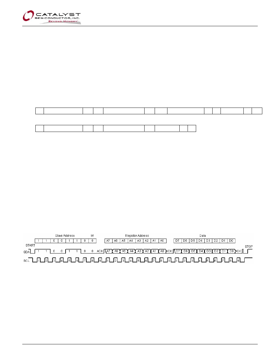
I
2
C INTERFACE
The LED driver is interfaced through a 2-wire serial
I
2
C-bus in order to control the state and the current in
each of the six LED channels. The SDA and SCL lines
comply with the I
2
C electrical specification and should
be terminated with pull-up resistors. When the bus is
not used, both lines are high. The device supports the
maximum bus speed of 400kbit/s. The serial bit
sequence is shown below for read and write operations
into the registers. Read and write instructions are
initiated by the master controller/CPU and
acknowledged by the slave LED driver. The I
2
C
address of the driver is internally fixed to the binary
value 1100110. The protocol requires that the start bit
and the device address are both repeated. For further
details on the I
2
C protocol, please refer to the I
2
C-Bus
Specification, document number 9398 393 40011, from
Philips Semiconductors.
Read
operation:
S
Slave address
W
A
Register address A S Slave
address R A Data A* P
Write
operation:
S
Slave address
W
A
Register address
A
Data
A P
S:
Start
condition
R, W: Read bit (1), Write bit (0)
A: Acknowledge sent by the slave LED driver (SDA high)
A*: Not Acknowledge sent by the master microcontroller (SDA low)
P:
Stop
condition
Slave address: Device address 7 bits (MSB first, slave address is 1100110).
Register address: Device register address 8 bits
Data: Data to read or write 8 bits
Write Instruction Sequence
CAT3626
Doc. No. MD-5014 Rev. C
12
© Catalyst Semiconductor, Inc.
Characteristics subject to change without notice
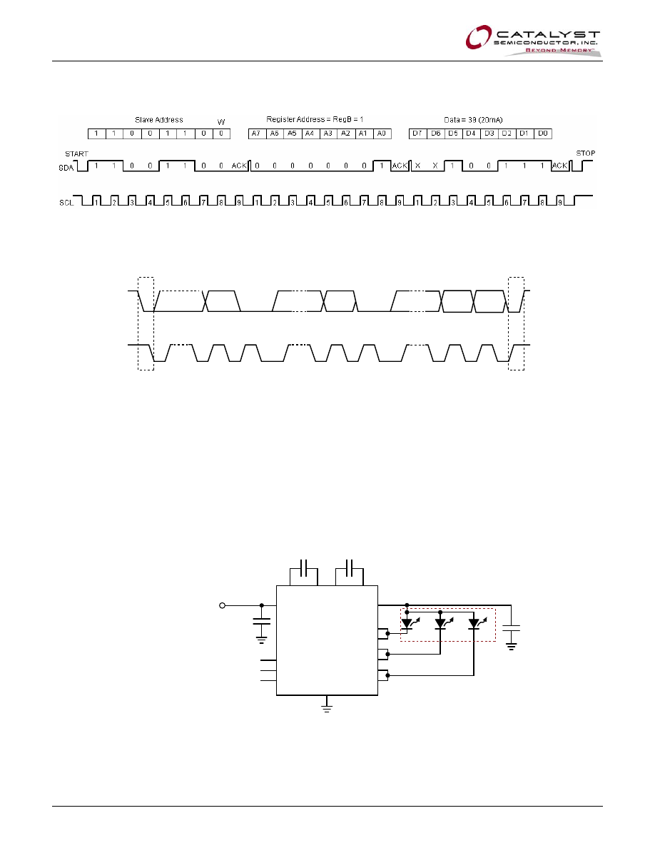
Write Instruction Example setting 20mA current in LEDB1 and LEDB2
I
2
C Bus Protocol
TYPICAL APPLICATION
The CAT3626 is ideal for driving RGB (red green blue)
LEDs with common anode configuration. The individual
LED currents associated with the red, green and blue
LEDs are programmable independently through the I
2
C
interface, allowing to generate an accurate color
mixing. Dimming while maintaining the same color can
be done by reprogramming the RegEn register on and
off with the appropriate duty cycle (PWM mode).
RGB LED
Red
Green
RGB LED
Blue
1µF
C
OUT
GND
V
IN
3V to
5.5V
LEDA1
LEDA2
LEDB1
LEDB2
LEDC1
LEDC2
EN
CAT3626
VIN
VOUT
1µF
1µF
C
IN
C1+
C1-
C2+
C2-
SDA
SCL
1µF
ENABLE
I
2
C Interface
SDA
SCL
START
Condition
ADDRESS
1-7
8
9
8
9
8
9
1-7
1-7
ADDRESS
R/W
ACK
ACK
ACK
DATA
STOP
Condition
CAT3626
© Catalyst Semiconductor, Inc.
13
Doc. No. MD-5014 Rev. C
Characteristics subject to change without notice
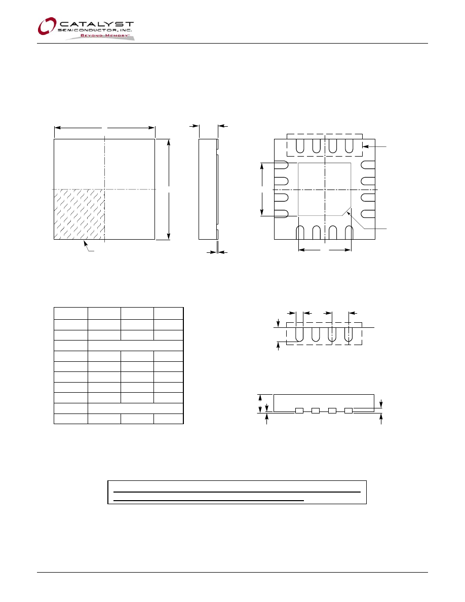
PACKAGE OUTLINE DRAWING
TQFN 16-Pad 4 x 4mm (HV4)
Notes:
(1) All dimensions are in millimeters.
(2) Complies with JEDEC standard MO-220.
E2
A3
e
b
L
A
A1
SIDE VIEW
TOP VIEW
BOTTOM VIEW
E
D
PIN#1 INDEX AREA
PIN#1 ID
DETAIL A
DETAIL A
FRONT VIEW
A1
A
D2
SYMBOL
MIN
NOM
MAX
A
0.70
0.75
0.80
A1
0.00
0.02
0.05
A3
0.20 REF
b
0.25
0.30
0.35
D
3.90
4.00
4.10
D2
2.00
2.10
2.20
E
3.90
4.00
4.10
E2
2.00
2.10
2.20
e
0.60 BSC
L
0.45
0.55
0.65
CAT3626
Doc. No. MD-5014 Rev. C
14
© Catalyst Semiconductor, Inc.
Characteristics subject to change without notice
EXAMPLE OF ORDERING INFORMATION
Notes:
(1) All packages are RoHS-compliant (Lead-free, Halogen-free).
(2) The standard lead finish is NiPdAu.
(3) The device used in the above example is a CAT3626HV4–GT2 (TQFN, NiPdAu Plated Finish, Tape & Reel 2000).
(4) For Matte-Tin package option, please contact your nearest Catalyst Semiconductor Sales office.
Prefix
Device #
Suffix
CAT 3626
HV4
– G
T2
Product Number
3626
Tape & Reel
T: Tape & Reel
2: 2000/Reel
Lead Finish
G:
NiPdAu
Blank: Matte-Tin
(4)
Package
HV4: TQFN 4 x 4mm
Optional
Company ID
REVISION HISTORY
Date Rev.
Reason
03/20/2006 A
Initial
Issue
11/19/2007 B
Added MD- to document number
Update Ordering Information
Update Package Outline Drawing
Added Example of Ordering Information
01/07/2008
C
Add Extended Temperature Range
Catalyst Semiconductor, Inc.
Corporate Headquarters
2975 Stender Way
Santa Clara, CA 95054
Phone: 408.542.1000
Document No: MD-5014
Fax: 408.542.1200
Revision: C
date:
01/07/08
Copyrights, Trademarks and Patents
© Catalyst Semiconductor, Inc.
Trademarks and registered trademarks of Catalyst Semiconductor include each of the following:
Adaptive Analog™, Beyond Memory™, DPP™, EZDim™, LDD™, MiniPot™, Quad-Mode™ and Quantum Charge Programmable™
Catalyst Semiconductor has been issued U.S. and foreign patents and has patent applications pending that protect its products.
CATALYST SEMICONDUCTOR MAKES NO WARRANTY, REPRESENTATION OR GUARANTEE, EXPRESS OR IMPLIED, REGARDING THE SUITABILITY OF ITS
PRODUCTS FOR ANY PARTICULAR PURPOSE, NOR THAT THE USE OF ITS PRODUCTS WILL NOT INFRINGE ITS INTELLECTUAL PROPERTY RIGHTS OR THE
RIGHTS OF THIRD PARTIES WITH RESPECT TO ANY PARTICULAR USE OR APPLICATION AND SPECIFICALLY DISCLAIMS ANY AND ALL LIABILITY ARISING
OUT OF ANY SUCH USE OR APPLICATION, INCLUDING BUT NOT LIMITED TO, CONSEQUENTIAL OR INCIDENTAL DAMAGES.
Catalyst Semiconductor products are not designed, intended, or authorized for use as components in systems intended for surgical implant into the body, or other
applications intended to support or sustain life, or for any other application in which the failure of the Catalyst Semiconductor product could create a situation where
personal injury or death may occur.
Catalyst Semiconductor reserves the right to make changes to or discontinue any product or service described herein without notice. Products with data sheets labeled
"Advance Information" or "Preliminary" and other products described herein may not be in production or offered for sale.
Catalyst Semiconductor advises customers to obtain the current version of the relevant product information before placing orders. Circuit diagrams illustrate typical
semiconductor applications and may not be complete.
Document Outline
- CAT3626
- 6-Channel LED Driver with I2C™ Interface
- FEATURES
- APPLICATIONS
- PRODUCT DESCRIPTION
- ORDERING INFORMATION
- PIN CONFIGURATION
- TYPICAL APPLICATION CIRCUIT
- ABSOLUTE MAXIMUM RATINGS
- RECOMMENDED OPERATING CONDITIONS
- ELECTRICAL OPERATING CHARACTERISTICS
- A.C. CHARACTERISTICS
- TYPICAL CHARACTERISTICS
- PIN DESCRIPTIONS
- PIN FUNCTION
- BLOCK DIAGRAM
- BASIC OPERATION
- LED CURRENT SETTING
- I2C INTERFACE
- TYPICAL APPLICATION
- PACKAGE OUTLINE DRAWING
- EXAMPLE OF ORDERING INFORMATION1
- REVISION HISTORY
Wyszukiwarka
Podobne podstrony:
High Efficiency 12V White Led Driver
ART3653A led driver 6 10szt
HV9910B LED DRIVER
AMC7150 ReferenceDesign LED DRIVER
Diody prostownicze, stabilizacyjne, LED
Oswietlenie LED do akwarium id Nieznany
Kolejny miernik na ICL7107 i wyświetlaczach LED wspólna anoda schemat
30 LED Projects
drivers data tab 1
Embedded Linux Kernel And Drivers
21 Montaż oświetlenia LED przestrzeni stóp
Constant current driving of the RGB LED
alpa led 4 kk EMM7XJKOQ7YNP6ZMH Nieznany
6Ż52P driver
Wyposażenie SHARANA w LED
iody led sprawko
Diody LED
How to install HD Audio driver?ter installation of slipstreamed XP SP3
sprawko led
więcej podobnych podstron