
Frequently Asked Questions
This page is not intended to replace the Design Tutorial in PCB Artist, but to clarify
important items for users. The Design Tutorial is found in the PCB Artist application
itself. It is accessible from the main menu under Help>Design Tutorial.
More information is available in the User Tips Guide for PCB Artist, which can be downloaded
from this
link
:
Email technical support is available at
layouthelp@4pcb.com
Contents
Component Creation and Library Manager
Q: Can I create my own components?
Q: Can I get a quick overview of the Schematic Symbol Wizard?
Q: Can I get a quick overview of the PCB Symbol Wizard?
Q: Can I get a quick overview of the Component Symbol Wizard?
Q: How do I create a connector or other manually created parts?
Q: I cannot find the part I am looking for. Am I not looking in the right place?
Q: How do you make mounting holes?
Q: How big should I make a finished hole size?
Q: How big should I make the pad size?
Q: Do I need to make Soldermask clearances?
Q: How do I place pads dimensionally on my part?
Q: How can I verify that the Component Symbol I created is correct?
Schematic Creation
Q: How do I create a Multipage Schematic?
Q: How do I Implied Connections?
Q: Where can I find power and ground symbols for schematics?
Q: How do I change the values of capacitors, resistors, etc?
Q: I made the symbol, but it doesn’t show on the list for Add Component. Why is that?
Q: How do I display pin logic names on the schematic?
The New PCB Wizard
Q: Can I change the board size later?
Q: What does Unit Precision mean on the Board page of the New PCB Wizard?
Q: What is a Board Template?
Q: I don’t know how many layers I need on the Layers page, what do I do?
Q: I need a split plane and a mixed plane inner layers, how do I specify that on the Layers page?
Q: On the Board Parameters page of the New PCB Wizard, I don’t know the minimum track width and
space I need. How do I handle that?
Q: On the Board Parameters Screen of the New PCB Wizard, I see the options for v-score and Tab rout,
but they are grayed out. How can I select those?
Q: What should I use the Special Requirements text box of the Additional Requirements page for?
Q: On the Production page, must I enter a part number and revision?
Q: I want an array, how do I configure it?
Q: When I ran the New PCB Wizard, I chose some options I need to change. Do I have to start over?
PCB Design Edit
Q: The plane layers are just a bunch of pads, what happened?
Q: How big should I make via pads?
Q: I created plane layers and they don’t have thermal connections. What happened?
Q: How can I change a component to the other side of the board?
Q: How do I display just the layers you want to see?
Q: When I display the Properties of an object the size shows as zero, but that can’t be right.
Q: I can’t seem to draw at odd angles, is it possible to do that?
Q: Can I make Mixed and Split Planes?
Frequently Asked Questions
1 z 33
2010-07-12 18:29

Q: How do I draw on a different layer?
Q: I have a net highlighted. How do I turn off the highlight?
Q: Can I make draws with 45 degree angles to the bends in my traces?
Q: How do I select all the segments of a trace at once?
Q: I need to change a pad (or trace) size universally, is there a faster way that editing the properties on
each one?
Q: How do I set up a Pour Copper area?
Q: I created a copper pour area, but it’s not filled. Is that correct?
Q: I have added new holes and traces in an existing copper pour. They are not on the net of the
copper pour, but they are connected to it. How do I fix this?
Q: I created a copper pour area and filled it. But it looks like the bounding box I drew the shape with is
still there, intersecting traces that aren’t on that net. Is that really shorting the nets?
Q: How close do I need to keep the copper pour from the rout edge?
Q: I cannot select what I wish to select. Other items at the same point keep getting selected. How can I
select the feature I want?
Q: How do I edit the soldermask?
Q: How do I make mounting holes?
Q: How do I create Slots?
Q: How do I put a radius or chamfer on my rout corner?
The Autorouter
Q: I have a fine pitch part that will not autoroute in the PCB. Why not?
Q: How can I prevent the autorouter from drawing in a “keep out” area that I want it to avoid drawing in?
Design Rule Checks
Q: Are there other checks to run besides Tools>Design Rule Checks?
Q: How can I review design rule check errors effectively?
Q: I cannot get rid of all my design rule errors so I can investigate and edit them. How do I do that?
Q: What do these Design Rule Check errors mean?
Arrays
Q: What is an array (also referred to as a sub-panel, palette, etc)?
Q: How do I make an array for a design?
Q: Cant I just Copy and Paste to create the array and skip the other way?
Order Process Questions
Q: How do I place an order?
Q: I clicked on Output>Submit order and it says that I have errors. What should I do?
Q: The order process is looking for a .fab file. What is that?
Installation
Q: I am getting a windows warning saying "Due to a problem initializing a Microsoft OCX control the grid
cannot be displayed. This option has not been turned off in Preferences."
Q: Why do I get an error during installation saying I don’t have permissions to access a file?
Q: I am having an installation problem that may be due to a proxy firewall. How can I deal with this?
Q: I cannot find the directory where my design is stored. Where is it located?
Q: Are other operating systems supported?
Assembly
Q: How do I optimize the design for Advanced Circuits Assembly Services?
Best Practices
v
Do not use Delete to remove tracks for redrawing.
v
Be careful when joining nets.
v
Avoid overlapping copper pours where possible.
v
Do not use copper pours for contact lands.
v
If your surface mount is colored gray, it requires a crucial edit.
v
Make sure your power and ground nets are properly defined in Settings>Nets as Power or
Ground in the Class Column.
v
Plane layers cannot have draws or tracks on them.
v
Always create a new library for any parts you create or modify.
v
In Settings>Spacings, never change the Board row to less than .020” or the Shape row to
less than .010”.
v
Do not create parts with the same name as any other part in any other library.
v
Do not add Vias inside Surface Mount Lands.
v
Always use Thermal Pads in Copper Pours for component holes.
v
Preventing accidental edits.
Frequently Asked Questions
2 z 33
2010-07-12 18:29

Component Creation and Library Manager
Q:
Can I create my own components?
A: Yes. There are millions of parts in circulation; it is not possible to pre-package a library with all
parts in it. There is a downloadable tutorial available for creating parts.
This link will download that
PDF tutorial
.
Procedure for getting maximum benefit from the Part Creation Tutorial:
1.
The tutorial builds a part step-by-step. Build that part in PCB Artist along with the
tutorial.
2.
Refer to the overview of the PCB Symbol Wizard and Manual Part Creation in this
document.
3.
Note down any questions you have in the process.
4.
Email the questions to
layouthelp@4pcb.com
when you have completed the tutorial.
Q:
Can I get a quick overview of the Schematic Symbol Wizard?
A: Here is an overview:
Schematic Symbol Creation
1.
Click on the Schematic Symbols tab in the upper left of the Library Manager.
a.
Click on the New Lib button in the upper right. This will create a new Library for your
part. Always put edited or created symbols of any kind in a library you created or you
risk losing them in the future.
b.
Click the Wizard button in the center column.
c.
i.
Click Next on the 1
st
page
ii.
Choose the Units and make the Precision 4 if you use Inches, Precision
3 if you use mm, and 1 if you use mils. Click Next.
iii.
Choose one of the schematic shape symbols. In the upper right, change
the Origin radio button to Pin1. Click Next
iv.
On the Styles page, leave all at the defaults and click Next.
v.
On the Pins page, distribute the pins on each side of the symbol as you
wish. Leave the Distance between Pins, Width across Symbol, and Length Of
Pin Leg all at the defaults. Click Next.
vi.
On the Finish page, Name the symbol. Click on the Save Symbol to
Library checkbox and change the dropdown to the library you created above.
Click off the Edit Symbol New checkbox. Click Finish.
Q:
Can I get a quick overview of the PCB Symbol Wizard?
A: Here is an overview:
1.
Look up the data sheet of the part you need to create from the distributor or
manufacturer.
a.
Warning: If the data sheet shows a PCB footprint (which is rare), you should
create to that footprint exactly as specified by the manufacturer.
b.
Some types of specified footprints are easier to manually create (see below for
manual part creation), than to create with the wizard.
c.
Parts with no specified PCB footprint are usually easier to create in the PCB
Symbol wizard.
2.
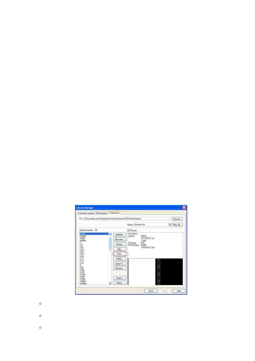
Go to the Library Manager, which is on the top icon bar. It is the fifth icon from the left
that resembles a book.
3.
Click on the PCB Symbols Tab.
4.
Click the Find button in the middle column. Search for the exact name you wish to call
the part you will create. No two parts in the library can have the exact same name.
Confirm the exact name is not used anywhere else.
·
IMPORTANT - All parts you make or edit must be placed in a library of your own
creation. They should never be placed in a library that came pre-packaged in PCB
Artist. When upgrading PCB Artist, all of the pre-packaged libraries will be
overwritten and new or modified parts residing in them. That directory can
be backed up in advance of the upgrade, but the best practice to prevent data loss
is to create your own libraries to store your new parts and also parts you have
modified.
5.
Click the New Lib Button on the upper right. This will create a new library and you will
Frequently Asked Questions
3 z 33
2010-07-12 18:29

be asked to name it.
6.
Click the Wizard button in the center column of buttons.
7.
In the wizard Start page, click the Next button.
8.
In the Technology page of the wizard:
a.
You can choose to use a Technology file. Technology files save many types of
settings from previous parts, such as Styles settings, Units settings, etc.
b.
Units: This can be independently set from the schematic or layout units that you
will use in your design. This should be set to the same units that the part’s data
sheet.
c.
Unit Precision: This controls how many decimal places are shown after the whole
number of any displayed or entered numbers.
i.
For example, if the Precision is set to zero and the Units are inches,
a .250” hole would show as size zero.
ii.
If the Units are set to millimeters and the Precision is set to 1, the
user can enter a .25 grid to in Settings>Grids but the system will change it
to .3.
d. Click the Next button.
9.
On the Type page there are several packages to choose from. Choose SOIC for this
example. Click the Next Tab.
10.
On the Pads page you specify the dimensions of the part from off of the datasheet of the
manufacturer.
a.
A representation of the part is constructed on the right. It adjusts as you change
values.
b.
Notice that if you change the number of pads, the symbol changes on the right to
match.
c.
The gold and gray colored rectangle in the bottom center of the page:
i.
Viewed from looking down upon it.
ii.
The gold is the pcb surface mount land.
iii.
The gray is the actual lead as it will sit on the surface mount land.
iv.
The “H” dimension controls the heel, which in PCB Artist is defined
as the sides and heel.
v.
The “T” dimension controls the toe.
vi.
The “PW” and “PL” dimensions represent the actual size of the
surface mount.
d.
Click Next to continue.
11.
The Silkscreen Shape page is for specifying the details of the silkscreen. Click the Next
Page.
12.
The Placement Outline page is for specification of the part outline that will be placed on
the Document layer. That layer can serve as an assembly drawing. Click the Next
button.
13.
The Finish page is where you save the part and specify its library. Make certain you are
saving to a new library of your own creation.
Q:
Can I get a quick overview of the Component Symbol Wizard?
A: Here is an overview:
1.
Creating the Component. This will join the schematic and PCB Parts.
In the Library Manager, click the Component Symbols tab in the upper left.
d.
Click on the New Lib button in the upper right. This will create a new Library for your
part.
e.
Click the Wizard button in the central column.
f.
i.
Click Next on the Start Page.
ii.
Choose Normal Component and click Next.
iii.
Details page:
1.
Component Name will be the name of the symbol in the library.
2.
Package is the type of package, you can type one in if you do not like
the ones listed in the drop down menu. These names do not have any
particular attributes that impact the part of its function.
3.
Default Reference is the name the reference designator that will show
on the silkscreen in the PCB layout.
4.
Component Pins is as the name suggests. In selecting the part, it will
only show PCB Symbols with this pad count in a particular library.
Frequently Asked Questions
4 z 33
2010-07-12 18:29
5.
Number of Gates. For this type of part, just leave it at the default 1.
6.
Click Next.
iv.
Schematic Symbols page, first choose the library the Schematic Symbol
was saved to, then select that part on the left. Make sure the Preview button
is clicked on. Click Next.
v.
PCB Symbol page works the same as the Schematic Symbols page.
Make sure the Preview button is clicked on. Click Next.
vi.
Assign Pins page, click the Assign 1 to 1 button. Click Next.
vii.
Finish Page, choose the Component Symbol library you had created
above. Make sure the Edit Symbol Now button is checked if you want to assign
logic names to the pins, if you do not want that you must un-check this
checkbox. Click Finish and the Component Symbol Editor will launch.
Manual Component Symbol editing.
2.
The Gates column will be with only one gate, that is as is should be.
a.
The SCH Symbol Name column should be left as is.
b.
The SCH Symbol Terminal Name is where you can enter the logic names of the pins of
the part. You do not have to enter them, but if you do not, they will not show on your
schematic. On a BGA, it will likely be too crowded to display them.
c.
The next three columns are for pin association. They should have the exact same
number in each row.
d.
The Net Class Name column should be empty.
e.
Go to File Save. Exit the part.
f.
Making the logic names show in the schematic.
3.
Select the specific component, right-click and go to Properties.
a.
Click on the Pin Names and Pin Numbers checkboxes to see those items.
b.
Click OK to exit and save your change.
c.
The logic names of a pad can be seen in the Status Bar in the lower left frame of the
application without displaying them in the PCB Design.
d.
Q:
How do I create a connector or other manually created parts?
A: There are no connector templates in the PCB wizard. This is the process to create one. There
are many other types of parts that are so different in footprint variation that they cannot have a
common template in the PCB symbol wizard. These must be created manually.
1.
Look up the data sheet of the part.
a.
Warning: If the data sheet shows a PCB footprint (which is rare), you should
adhere to that exact footprint in regards to hole sizes and any surface mount land
patterns. Thru-hole pads should use a pad that has no less than .014” annular
ring.
2.
Most Data sheets use relative dimensions to define the part. We must manually convert
all of these to absolute dimensions from of a point we can easily reference.
a.
Print out the data sheet, it is recommended to blow up the dimensioned area.
Use a pencil to make the conversions and note these absolute dimensions on the
print-out as seen in the example below (the notes are in red).
Frequently Asked Questions
5 z 33
2010-07-12 18:29
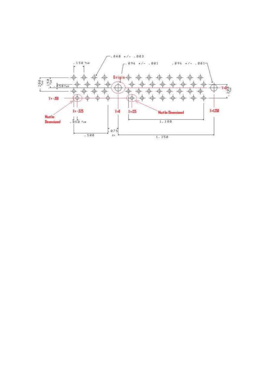
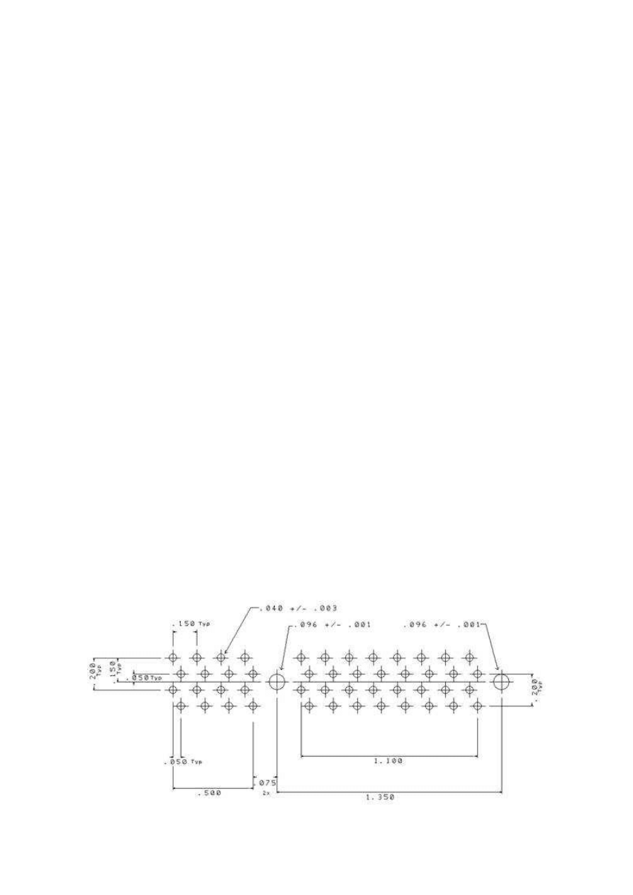
b.
Choose an easily accessible point on the part as the origin from which all absolute
dimensions will reference. In the graphic example below, the indicated hole will
serve as the origin and all manually converted absolute dimensions referencing it
are in red.
c.
You must always determine the x and y location of each mounting hole and also
the lower left component hole of each grid of component holes.
3.
Go to the Library Manager, which is on the top icon bar. It is the fifth icon from the left
that resembles a book.
4.
Click on the PCB Symbols Tab.
5.
Click the New Lib Button on the upper right.
·
All parts you make or edit must be placed in a library you have created.
·
When upgrading PCB Artist, prepackaged libraries will be overwritten (unless they
are backed up in advance). To prevent data loss, the best practice is to make new
libraries.
6.
Click on the New Item button. This opens an editing screen similar to the Edit PCB
screen.
7.
Making your pad and hole sizes.
a.
Go to Settings>Units and set the units to the type used in the part drawing. In
this example, use Inches with Precision set to no less than 3.
b.
Go to Settings>Styles.
c.
Click on the Pads Tab.
d.
Making the Component Pads Style:
i.
Click on the Add Style button
ii.
Give the pad a name. This is its Style Name, which you should
note down. For this example, call this CompPad1.
iii.
Make Drill the finished hole size suggested by the manufacturers
drawing. In this example .040”
iv.
Make the pad (Width) no less than .014” (.36mm) over the hole
size. In this example, the hole is .040” and the pad is going to be no less
than .054”.
v.
Click on OK to add the Style.
e.
Creating the Mounting Holes Style:
i.
Click on the Add Style button
ii.
Give the mounting hole a name. This is its Style Name, which you
should note down. For this example, call this MountingHole1.
iii.
Make Drill the finished hole size suggested by the manufacturers
drawing. In this example .096”
iv.
Make the pad (Width) the same size as the mounting hole, .096” in
this example. The pad exists as a presence on Top Copper for other
features such as Pour Copper to avoid. In manufacturing, the pad will be
removed.
v.
Click off the Plated checkbox.
vi.
Click OK to save and exit the dialog.
vii.
A warning will say that the drill completely removes the pad.
Frequently Asked Questions
6 z 33
2010-07-12 18:29

viii.
Click OK to save and exit the Styles dialog
8.
Place the Mounting holes.
a.
Placing the Origin.
i.
Because the datum is a mounting hole, we must place them first.
The origin position defaults to the first pad placed.
ii.
Click Add Pad, drag the cursor to the work area, but do not add it
yet.
iii.
Click the <s> hotkey to choose the Style of pad to add. Choose the
mounting hole you had made from the list.
iv.
Add the pad.
v.
Change to Select mode by clicking the white cursor arrow far right
icon on the top icon bar. The icon looks like the cursor.
vi.
Select the pad, right-click on it, and choose Origins>Set System
Origin At Item (NOT “At Cursor”) from the right-click context menu.
1.
All dimensions displayed or entered in the design are now based off
the center of this pad.
b.
Placing the second mounting hole.
i.
Click Add Pad.
ii.
The Style will be the same as the last one used, so it’s not
necessary to change it.
iii.
Place it anywhere.
iv.
Change to Select mode by clicking the far right icon of the top icon
bar. The icon looks like the cursor.
v.
Select the pad that was just placed, right-click over it and go to
Properties.
vi.
In Properties, Type its destination X and Y axis coordinates in the
Position fields. In this example, those coordinates are X=1.35, Y=0.
vii.
Click OK. The mounting hole will move to those target coordinates.
9.
Placing the grid of component pads.
a.
Go to Settings>Grids. Click on the Working Grid Tab.
b.
Change the first textbox of the Step Size section to the X axis coordinate of the
lowest component pad in the far left. In this example, that is .525” (the true
coordinate is -.525”, but the grid system does not accept negative numbers and a
negative number is not necessary).
c.
Click on the Different Y checkbox. In that blank type in the Y axis coordinate of
the lowest component pad in the far left. In this example, it is .150” (the true
coordinate is -.150”, but the grid system does not accept negative numbers and a
negative number is not necessary).
d.
Click OK to accept the changes and exit the Grid dialog.
e.
Click on Add Pad. Drag your cursor to the work area, but do not place any pads.
f.
Right Click and choose Add Multiple from the right-click context menu.
g.
The Add Multiple dialog window:
i.
In the Number of Items section, we must set how many pads we
are adding in the X and Y.
Frequently Asked Questions
7 z 33
2010-07-12 18:29
1.
In the X, we are setting 4 component pads (for this purpose, ignore
the stagger on every other row). Set the X to 4
2.
In the Y we are also using 4 in the Y axis. Set the Y to 4.
3.
Many options on this screen that were grayed out are now editable.
ii.
The Step Offset Section.
1.
The X is the center-to-center distance between pads in the X axis.
In this example, enter .150” in the X.
2.
The Y in this example is .100”. Ignore the shift offset for now. In
this example enter .100” in the Y.
iii.
The Insert Order Section.
1.
In this case, make sure the toggle is set to Insert Row. This is due
to the fact that every other row is staggered. (If changed to Insert
Column, then every other column would be staggered.)
2.
Stagger Pitch is to establish how much the 2
nd
row is staggered
from the 1
st
. If set to Insert Row, this is create a stagger (or
indent) an X axis dimension. If set to Insert Column, it would be a
stagger in the Y axis dimension. In this case the stagger is -.050”
(the negative number is allowed and necessary). The negative
number means the 2
nd
row will start further to the left than the 1
st
row. If the drawing showed the second row starting to the right, it
would be a positive number (.050”). Enter -.050”.
iv.
Click Ok to save your settings and exit that screen.
h.
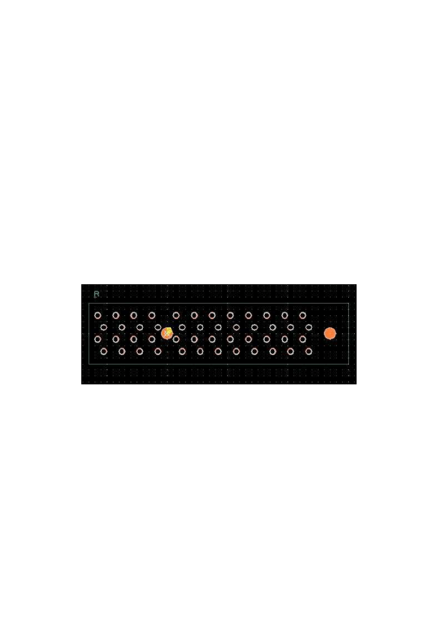
Click the <s> hotkey and choose the appropriate Style for this pad. In this
example, use CompPad1.
i.
Now move your cursor until it is at the correct position. Use the Status Bar
coordinates in the lowest left frame of PCB Artist to ensure you are at the correct
grid coordinates. Then click once to add that grid of component pads.
j.
Add the second grid of component pads using the same process as described
above, with these exceptions:
i.
Go to Settings>Grids and change the grid X to .125” and leave the
y as offset at .15.
ii.
Change the number of items in X from 4 to 8.
Frequently Asked Questions
8 z 33
2010-07-12 18:29
k.
Confirm the Dimensions are correct.
i.
Find each dimensioned pad, right click on it and choose Properties
from the right-click context menu. Confirm that the coordinates displayed
in Properties are correct.
ii.
Use Origins>Set System Origin At Item to change your origin to
confirm that the part data sheets original relative coordinates are correct.
iii.
Warning: Confirm every relative coordinate on the data sheet.
1.
This verifies:
a.
That the conversion to relative coordinates was done
correctly.
b.
That nothing was incorrectly typed in.
c.
That no assumptions or oversights occurred during the
entire process.
2.
Be aware that occasionally a manufacturer’s data sheet is
incorrect, and the numbers do not add up. At this point the part
manufacturer would have to be contacted for the correct
dimensions.
10.
Legend Edits.
a.
Go to Settings>Grids and change your grid to a .050” grid. Click off the Different
Y checkbox and click OK to save the changes and exit the dialog.
b.
Click on Add Shape Rectangle
c.
Hit the <L> hotkey and change your layer to the Top Silkscreen (if it isn’t already
on the Top Silkscreen).
d.
Use Add>Shape Rectangle to add the legend outline of the part by clicking in the
lower left to start the rectangle and double-clicking on the upper right corner.
11.
Go to Add>Reference Origin and Click on any open area. The “+R” is a place holder for
the part’s reference designator. The actual reference designator text “Conn” would be
applied when editing the Component.
12.
Adding the Placement Outline.
a.
The Placement Outline is a box, often a bit bigger than the Legend outline.
b.
Add it in the same manner as the Legend.
c.
This outline will go on the Document1 layer (or the Document 2 layer in some
cases)
d.
The Document layers are usable for Assembly Drawing layers, and the outline can
serve that purpose, or can be used for many other purposes.
13.
Changing the Part Datum
a.
Find Pin 1 on the part Data sheet. In this example, it is the pin in the upper left.
b.
Select that corresponding pad on your part, right click on it and choose
Origins>Set System Origin At Item. That pad is now the 0,0 center.
c.
Select the “+S” symbol that is the Symbol Origin. You many need to use the <n>
hotkey to cycle through the different objects at that location until it is selected.
d.
Right click and choose Properties from the right-click context menu.
e.
Change its Position to 0,0. The Symbol Origin must always be on Pin 1.
i.
It is recommended to always put the System Origin on pin 1 so that
the pads on the PCB Grid. This make it much easier to route tracks to the
pads.
ii.
Some believe that placing the System Origin at the middle of the
PCB Symbol helps CPL file (component position file) generation. The
System Origin has no affect on the determining the center of components.
Placing the System Origin at the center will often cause all pads of the
Frequently Asked Questions
9 z 33
2010-07-12 18:29
component to not be on the PCB grid.
14.
Renumber Pins
a.
Pins are automatically numbered as they are added, including mounting holes.
So when we placed our mounting hole origin for this part, it became pin 1. We
must change this.
i.
To View the Pin Names more clearly, go to View>Colors. Click on
the Other Items tab of the Colors Dialog box in the upper left. Click on the
Pin Names Checkbox.
b.
Go to Edit>Renumber Pins.
c.
Click OK in the Renumber Pins dialog box to start numbering pins.
i.
Notice that in the Status Bar on the lower right application frame is
now in Renumber Pins mode.
ii.
You will also notice in the Status Bar the “Next Number” box
indicates the number 1. This is the number that next pad you click on will
be changed to.
d.
Click on pin 1.
e.
Click on each pin, in sequential order, until all the pins are numbered.
f.
Lastly click on each mounting hole, they also must have a pin number.
g.
Hit the <esc> key to exit Renumber Pins mode.
15.
Save the PCB Symbol to the Library you have created for it.
a.
Make certain that you are using a unique name that is not used anywhere else in
the library.
b.
You must add this new symbol to a Component Symbol to add it to any design,
regardless of whether it is being added to a schematic or a PCB design.
16.
Component Creation
a.
Any part that contains mounting holes cannot be created with the Component
Symbol wizard.
b.
Use the New Item button in the Library Manager’s Component tab to create any
components with mounting holes.
Q:
I cannot find the part I am looking for. Am I not looking in the right place?
A: The most effective search method is using this method:
From the main menu, go to File>Libraries.
1.
Click on the Component Tab.
2.
Use the Find button in the central row of buttons.
3.
Next to the Name field, Change the drop down menu from Is Exactly to Contains.
4.
It can also be very effective to search by pin number, unless the pin count is very small.
If you cannot find the part you are looking for in 5 minutes, you should just create it.
5.
Almost any part can be created in 5-15 minutes in PCB Artist, especially with the PCB
footprint wizard.
That new part can then be saved into a library you create and is organized in a way that
best suits your preferences.
Frequently Asked Questions
10 z 33
2010-07-12 18:29
Q:
How do you make mounting holes?
A: You can make them in two different ways:
1.
The Quick way:
a.
Use Add pad to place the pads.
b.
Use <cntrl> to select all of the pads to be changed.
c.
Right-click on any one of the pads and select Properties from the right-click
context menu.
d.
Change the Drill to the required finished hole size.
e.
Change the Width (which is the pad width) to the same size as the drill.
f.
Click off the Plated checkbox.
g.
A warning will say the drill removes the pad, click OK.
h.
This method will not give a Style name to these holes and will make it difficult to
group select the all of them by the Style name. This technically puts them into
the “Unnamed” Style group with many other shapes making them tedious to have
to select by group in the future.
2.
The Best Practices way:
a.
Go to Settings>Styles.
b.
Click on the Pads tab.
c.
Click the Add Style button.
d.
Enter a Name by which the new style will be referenced.
e.
Enter the Drill Size.
f.
Enter the Width (which refers to the pad width).
g.
Click off the Plated checkbox.
h.
Click the OK button to save and exit.
i.
An error message will say the drill removes the pad, click OK.
j.
Click Add Pad and drag your cursor over the work area, but do not yet add the pad.
k.
Click the <s> hotkey (or right-click and choose Change Style).
l.
In the dialog box that appears, choose the name of the style you created.
m.
Add the Pad(s).
n.
The advantage to creating a style is:
1.
You only need to go to Settings>Styles to edit all the holes in the group at one
time in the future.
2.
You have the ability to select and display all items using the Style in the Goto tab
of the Interaction Bar.
Frequently Asked Questions
11 z 33
2010-07-12 18:29

Q:
How big should I make a finished hole size?
A: Always research the manufacture’s part and use what they recommend.
·
In the event that the manufacturer provides no information and all other information
sources are exhausted, the hole should be make at least .010” over the thickness of the
lead. This is intended as a rule of thumb. The burden of research and verification that
the rule applies to a particular design scenario is upon the designer.
Q:
How big should I make the pad size?
A: The minimum requirement is a pad that is .014” over the hole size. So for a .020” hole, make
at least .034”.
Q:
Do I need to make Soldermask clearances?
A: Here is now the soldermask layer works:
Thru-hole pads are placed on layer [All] automatically. This means they have pads on all
layers when added to or translated into a PCB. This includes an automatically generated
soldermask clearance of exactly the needed size.
If you use the PCB Footprint wizard, it will automatically place surface mount devices on the
[Top] layer. The [Top] layer automatically creates a clearance for the surface mount device
on the Top Copper layer, the Top Soldermask layer, and the Top Solder Paste layers.
If you place a surface mount component on a PCB and use Flip to change it to the solderside,
all [Top] values automatically become [Bottom] and all other relationships to layers are
treated accordingly.
If you need a soldermask clearance that does not correspond to a specific pad, such as a large
soldermask clearance over the whole component, use Add Shape. Use the <L> hotkey to
change your working layer to the Top Soldermask. Draw the polygon and then select any
segment of it, right-click and choose Properties from the right-click context menu. In
Properties, click on the Filled checkbox.
Use the Layers tab of the Interaction Bar to display only the Top Solder Mask layer(s) to
view the shapes.
Be aware that all objects on the soldermask are clearances in the soldermask and everything
that is black in the soldermask layer will have the green soldermask covering.
WARNING: If you create a contact land with copper pour it will NOT have a soldermask
clearance. Copper pour is not the correct tool to make contacts with. A solder mask clearance
would have to be manually created using Add Shape Polygon to create the cleared area on the
appropriate soldermask layer and then go into the polygon’s Properties to click on the Filled
checkbox.
WARNING: If you Add Pad and then use Properties to make it a surface mount, it will be
associated to the [All] layer, where all thru-hole pads live, and will be present on every layer.
Surface mounts must be on layer [Top] or [Bottom]. The netlist will also believe the surface
mounts have an electrical connection to the other surface mount counter parts on the other
layers, were none exists, and will display the ratsnets and autoroute accordingly.
Frequently Asked Questions
12 z 33
2010-07-12 18:29
Q:
How do I place pads dimensionally on my part?
A: This is the process:
Print out your data sheet for the part.
1.
Data sheets usually have relative dimensions. We need to manually create absolute
dimensions to an origin which can be easily referenced on the design. Manually convert all
dimensions to their absolute dimensions from that origin. You can place a pad to serve as the
origin and delete it later if necessary (but this will require the use of Edit>Renumber Pins to
correct).
2.
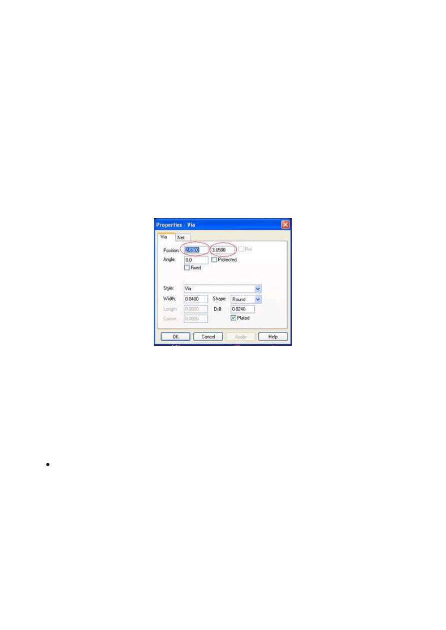
Right click on the datum and click Origins>Set System Origin At Item. The displayed
coordinates and grid will now be snapped to that object.
3.
Go to Settings>Styles of the objects that need to be placed dimensionally.
4.
Click Add Pad, drag the cursor over the work area, and hit the <s> to choose the Style to be
added. Place the objects anywhere in the work area.
5.
Select each object, right-click and choose Properties from the right-click context menu. Type
in their absolute coordinates. When you click OK to save your edit and exit Properties, the
object will move to those coordinates.
6.
When all items are placed, change your origin as necessary to confirm all relative and
absolute coordinates.
7.
Q:
How can I verify that the Component Symbol I created is correct?
A: Use this method:
After creating your part create a blank schematic by clicking on File>New.
1.
Bring up the Interaction Bar (use the <F9> key to bring it up and also to hide it).
2.
Click on the Add Component tab of the interaction bar.
3.
At the top of the Interaction Bar, select the library of the part you created.
4.
Select the part you created and drag it to the blank schematic.
5.
Go to Tools>Schematicß>PCB>Translate To PCB.
6.
Watch for an error message. An error message indicates that something is wrong in the
Component Symbol.
7.
This method allows a new user to verify they have built their first few parts correctly without
finding out there is a problem after the entire schematic is laid out with many components
requiring corrections.
Schematic Creation
Q:
How do I create a Multipage Schematic?
A: Here is the process:
Go to File>New and chose a Project.
1.
Then go to File>New and choose a new Schematic. Check the box at the bottom of the dialog
to Add To Open Project.
2.
Page frames for the schematic can be found in the Schema library.
3.
Off page references between schematic pages are made simply by the nets having the same
4.
Frequently Asked Questions
13 z 33
2010-07-12 18:29
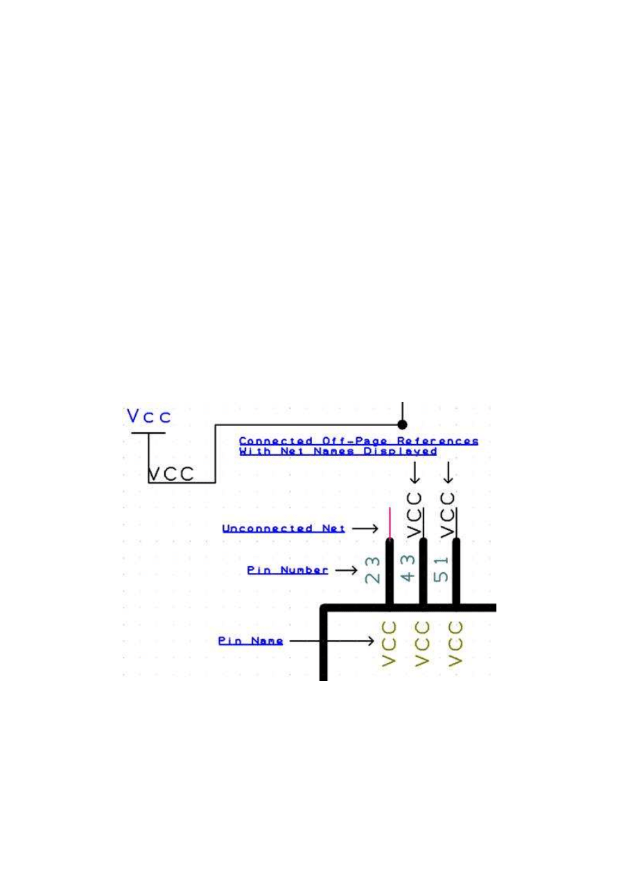
name set in Settings>Nets.
This does not apply to generically named nets (the “N0000” named nets). Generic nets
are local to the page they are on only.
a.
In Settings Nets, if a GND net is created and it exists on another page, they will connect
whether or not a connection or off page reference is drawn.
b.
In the Implied Connection instructions (the topic directly below) also apply to off page
references between Project sheets. However, the hanging connection will turn red
indicating it is unconnected. It will connect due to the net associations, despite
appearing unconnected. To make this clearer and to remove the hanging connection
highlight, use the To and From symbols of the Schema library. Those symbols do not
have any special attributes, the net name itself is all that is needed to make the
connection.
c.
Splitting component gates is best covered in Help section of PCB Artist. Go to Help>Contents
and type into the search blank the “project gates”. Click on the topic “Splitting Components
Across Schematic Designs” for complete details.
5.
Q:
How do I Implied Connections?
A: This is the process:
Draw a connection off of a pin. Drag it a few grid points and double-click to terminate it
there. The connection will turn red to indicate an un-terminated connection.
1.
Select the connection, right-click and choose Change Net from the right-click context menu.
Choose the net that you want it joined to.
2.
The color of the connection should change to black to indicate the connection is no longer
un-terminated.
3.
Right click on the connection again and choose Display Net Name to verify the process was
successful at a glance.
4.
Q:
Where can I find power and ground symbols for schematics?
A: They are located in the Schema component library.
Q:
How do I change the values of capacitors, resistors, etc?
A: Use either a window selection or the <cntrl> button (in the same way you can use it to select
specific files in Windows Explorer) to select all the specific components of that type to have the
value changed. Then right click on any one of them and choose Properties. In the Properties
window, click the Values tab. Select the value in the list and use the Edit button to change it. All
the components will now have the new value.
Frequently Asked Questions
14 z 33
2010-07-12 18:29

Q:
I made the symbol, but it doesn’t show on the list for Add Component. Why is
that?
A: Schematic and PCB Symbols cannot be added to a board directly. They must be first joined into
a Component Symbol. Only Component Symbols can be added to a PCB or Schematic.
Q:
How do I display pin logic names on the schematic?
A: This is actually done at the component level.
Go to the Library Manager
1.
Click on the Component tab.
2.
Go to the correct library and select the part. Click the Edit button
3.
Enter the logic name in the Terminal Name column (third column from the left).
4.
Save and exit.
5.
Open the schematic and then go to Tools>Update Component.
6.
If the logic names are not displayed, right click on the component and choose Properties.
Click on the check box for Pin Names.
7.
If the Pin Names do not show, go to View>Colors. Click on the Other Items tab and click on
the Pin Names checkbox if it is checked off. Click OK to save your changes and exit the Colors
dialog box.
8.
The New PCB Wizard
Q:
Can I change the board size later?
A: Yes, you can delete it and completely redraw it in the PCB, but it must be created and finalized
before placing an order.
Q:
What does Unit Precision mean on the Board page of the New PCB Wizard?
A: Unit Precision is found in Settings>Units. Precision is how many decimal places any displayed
coordinates round up to. If you have the Units set to Inches and the precision is set to zero, then
the displayed size of a .250” hole will be 0”. Set Unit Precision appropriately for the units you have
selected. Recommended Precision for Inches is Precision 4, for Millimeters is Precision 3 and for Mils
is Precision 1.
Q:
What is a Board Template?
A: When you create PCB Designs, you can save as a template. That will save the board with all its
settings, components, board outline, and even tracks and copper pours. You can then use that
saved template to start a new design with all those features built in for future designs. It can be
used to save as little as unit settings or as much as whole designs. Be aware that if you save a
template for a design, the entire design is saved, not just select features.
Q:
I don’t know how many layers I need on the Layers page, what do I do?
A: It is easy to add layers after the New PCB Wizard, but when eliminating layers, you can only
eliminate the last inner layers. So if you create a 10 layer board and find out that you only need 6,
when you go to change the layer count you can only eliminate layers 9, 8, 7, and 6 (the Bottom
Copper will become the new layer 6). This also changes the possible plane layers to 2, 3, 5, and 6,
Frequently Asked Questions
15 z 33
2010-07-12 18:29

which may be a major conflict of some of those layers are already routed signal layers. So it is
recommended to start out with a small number of layers and then once the layout has progressed to
a point that the need for more layers is unavoidable, add the layers then from Settings>PCB
Configuration.
Q:
I need a split plane and a mixed plane inner layers, how do I specify that on the
Layers page?
A: The plane layers are intended as pure planes. They should never be edited under any
circumstance, even to draw a single track. On the layers page, leave them as signal layers and then
when editing the PCB, use Pour Copper to draw split and mixed planes.
Q:
On the Board Parameters page of the New PCB Wizard, I don’t know the minimum
track width and space I need. How do I handle that?
A: The default is 10 mils, you can change it in the design, but you will have to go to Settings>PCB
Wizard when you are in the PCB design and change this value on the Board Parameters page. The
system will not allow you to submit the order if this number is not correct. It will prompt you if this
value is different.
Q:
On the Board Parameters Screen of the New PCB Wizard, I see the options for v-score
and Tab rout, but they are grayed out. How can I select those?
A: Basic Design Requirement orders cannot have a v-score or tab route, due to overwhelming
request of customers seeking the lowest possible cost. This includes orders with arrays. To get
those options, select Expand Design Requirement on the Design Requirement Page of this wizard.
Q:
What should I use the Special Requirements text box of the Additional
Requirements page for?
A: It’s intended for any requirements that do not already have an option in the wizard and also for
extra details of items you can select. Some Examples:
If the board is a flex design and requires a thinner final thickness not listed on the board thickness
drop-down menu of the Board Parameters page (but was verified as possible for your design,
through PCB Artist Technical Support), this would be the place to specify it. Special billing or
shipping information can be noted here as well any special instructions. The board has
countersinks, use this space to specify the counter sinks and to differentiate which holes are the
countersinks. You can return to this page from Settings>PCB Configuration once you are in the
design.
Q:
On the Production page, must I enter a part number and revision?
A: Yes, we must have a way to reference the part for future orders. The software requires both of
those blank be filled out before order placement.
Q:
I want an array, how do I configure it?
A: See the Array section, below. That contains all instructions and examples.
Q:
When I ran the New PCB Wizard, I chose some options I need to change. Do I have
to start over?
A: Some options ran in the PCB Wizard can be changed long after PCB creation. This can be done
from the main menu click on Settings>PCB Configuration to change some values.
Warning: Reducing the number of layers in this manner can eliminate nets. If layers
must be eliminated, go to Output>Net Completion Report to get a report of the nets that are
now incomplete. Then from the main menu, go to Tools>Optimize Nets to make the
un-routed net connections appear. They can be manually or auto-routed from that point.
After they are routed, it would be wise to go to Output>Net Completion again to confirm
nothing was lost.
PCB Design Edit
Q:
The plane layers are just a bunch of pads, what happened?
A: Go to View>Powerplane>Show to view pure plane layers. Mixed and Split planes are technically
signal layers (using pour copper to make the planes), so those layers are viewed normally as any
Frequently Asked Questions
16 z 33
2010-07-12 18:29

signal layers is.
Q:
How big should I make via pads?
A: Make the via pad style 010” larger than the drill size. So for a .018” via hole, make the pad
style width .028”. Make certain that you are using the Via style in Settings>Styles or the Design
Rule Checks will not know they are intended as vias and will flag them as annular ring errors.
Q:
I created plane layers and they don’t have thermal connections. What happened?
A: In the New PCB Wizard, either no net names were assigned to the planes or they were not
spelled exactly the same as the net name (proper case is required as well).
To fix this, go to Settings>PCB Configuration in the PCB file and go to the Layers screen.
1.
Use the drop down menus for assigning the planes to the correct nets to ensure that nothing
is misspelled or has a different case.
2.
Go to View>Powerplane>Show and view each plane to confirm they now have thermal
connections.
3.
Q:
How can I change a component to the other side of the board?
A: Select the component, right-click on it and choose Flip.
Q:
How do I display just the layers you want to see?
A: Bring up the Interaction Bar with <F9> and Click on the Layers tab at the very bottom of the
Interaction Bar. Right-click over the list of layers and choose the All Layers Off option. Then click
on just the layers you want to view.
Q:
When I display the Properties of an object the size shows as zero, but that can’t be
right.
A: Go to Settings>Units and change the Unit Precision to a larger number. Precision is how many
decimal places any displayed coordinates round up to. If you have the Units set to Inches and the
precision is set to zero, then the displayed size of a .250” hole will be 0”. Set Unit Precision
appropriately for the units you have selected. Recommended Precision for Inches is Precision 4, for
Millimeters is Precision 3 and for Mils is Precision 1.
Q:
I can’t seem to draw at odd angles, is it possible to do that?
A: Yes
Click on the icon of the type of draw you wish to make (such as Add Track, Add Board Polygon,
Add Shape Polygon, Add Track, Add Copper Pour Area Polygon , etc.).
1.
Click to Add the draw and move your cursor to the work area.
2.
Before starting the draw, right click to open the context menu.
3.
Select Segment Mode>Free
4.
Now lines can be added at any angle.
5.
If moving shape segments, use the Free Rubberbanding option from the right-click context
menu to allow the attached segments to take any angle.
6.
Q:
Can I make Mixed and Split Planes?
A: Yes, on outer layers, just use Pour Copper. On inners, DO NOT make the intended inner layers
plane layers, keep them as signal layers. This can be modified while in the design from
Settings>PCB Configuration on the Layers page of that wizard. You can then create split and mixed
planes using Pour Copper just as it would be done on the outers. Never try to draw on a true plane
layer, not even a single trace.
Q:
How do I draw on a different layer?
A: Here is one way to do it.
Click on Add Track
1.
Right-click and choose Track Layer OR hit the <L> hot key.
2.
Click the box that says Apply To All Segments if want the whole track on the layer you are
switching to.
3.
Select the layer you wish to draw on in the dialog box that appears. It will automatically
default to a layer other than the one you are on, so just hit return to accept it if you are on a
4.
Frequently Asked Questions
17 z 33
2010-07-12 18:29

double-sided board and you will be on the Bottom Side automatically.
Q:
I have a net highlighted. How do I turn off the highlight?
A: The easiest way is from View>Highlight Net>Remove Highlight.
Q:
Can I make draws with 45 degree angles to the bends in my traces?
A: Yes
Click on the icon of the type of draw you wish to make (such as Add Board Polygon, Add
Shape Polygon, Add Track, Add Copper Pour Polygon, etc.).
1.
Click to add the start of the shape.
2.
Right Click to open the Context Menu while you are still in draw mode.
3.
Select Segment Mode>Miter.
4.
You can now draw at angles and the system will automatically put all junctions at 45 degrees.
5.
It may help to change your draw mode to Free. See the question above regarding drawing at
odd angles.
6.
Q:
How do I select all the segments of a trace at once?
A: Push and hold down the <shift> key, then select the trace. You can also select multiple whole
traces by pushing and holding down the <cntrl> and <shift> keys.
Q:
What is the significance of the pad colors?
A: On the default color settings:
Grey pads are present on all layers.
In Properties, they show as being on layer [All].
Surface mounts should not be grey. If they do, the component needs to be edited to
change them from layer [All] to layer [Top] (NOT to be confused with layer Top Copper!
An object on layer [Top] automatically has a soldermask clearance and solderpaste
clearance generated. I will also flip all those to the [Bottom] layer if the Flip option is
used on the component.
Dark Red pads (using the default color settins) are on Layer [Top] IF they are a slightly darker
red than the Top Copper traces. If they are the same shade of red as the traces, then they
are not on the [Top] layer, they are on Top Copper and will have no soldermask or solderpaste
clearance. They must be changed to layer [Top] in Properties (see previous bullet point).
Dark Blue pads (using the default color settings) are on layer [Bottom]. They are slightly
darker than the traces on the Bottom Copper Layer. The have all the other properties of
objects on layer [Top], described above.
Yellow pads are vias created by the application when using the autorouter, moving a track
segment to another layer, or other processes where the application places the hole
automatically. They are present on layer [All], but are not associated with a component.
Most commonly these are vias.
Q:
I need to change a pad (or trace) size universally, is there a faster way that
editing the properties on each one?
A: Yes, here is one of several ways to do this:
First determine the pad style used from the properties box.
1.
Go to Settings>Styles.
2.
The Styles window will open, click on the Pads tab.
3.
The names of each pad style are listed. A new style can be created or an existing style can be
edited from this window.
4.
Be careful to be sure that the change will not affect more pads than you intended to affect.
5.
Various combinations of selections and added styles can be used to accomplish different goals
in selectively changing styles.
The Interaction Bar’s Goto tab can be used as a powerful tool when set to styles. Right
clicking on the name of the style and choose Select All Find Items is another way to select all
the items and to see them all selected before editing them either with Properties or through
Settings>Styles as described above.
Frequently Asked Questions
18 z 33
2010-07-12 18:29

Q:
How do I set up a Pour Copper area?
A: Here is the process:
Draw the bounding box polygon Using Add>Copper Pour Area.
1.
·
You can draw right over the rout and the poured copper it will clip itself back from the
rout by the exact amount required (which is set in Settings>Spacings).
·
The copper pour will clip itself back from all objects in the area that are not on the same
net automatically (the spacing used is set in Settings>Spacings).
·
In Settings>Spacings, the Shapes row governs the distance the copper is clipped back
from the copper pour. The entire Shapes row must always be set to no less than .010”.
Click on the Selection Icon to exit draw mode (from the top icon bar, the last icon on the right
that looks like your cursor).
2.
Click on any one segment of the bounding box you just added.
3.
Right-click and choose Pour Copper from the right-click context menu.
4.
In the dialog box, choose the net it should be on. Leave that text field blank to have the
copper pour unconnected from a net.
5.
Click on the Thermal Pads checkbox to automatically add thermal pad connections.
6.
Click on the checkbox to remove Isolated Areas at the bottom of that dialog window. Isolated
areas will cause rats nests to show those areas as unconnected. Isolated areas will behave as
an antenna on the finished board. Another option is to use the Highlight checkbox and connect
those isolated islands with vias to their proper net.
7.
IMPORTANT - The copper pour is applied once to the area it fills. If changes are made after
the copper pour (such adding vias, mounting holes, or moving tracks) the copper pour will
NOT adjust to this new change. To have the copper pour adjust to those changes, simply
select the bounding box of the copper our, right click and click Pour Copper again. The Pour
Copper dialog box will appear with the exact same settings of the previous pour. Click OK and
the pour will be adjusted considering the changes made to the area.
8.
IMPORTANT – The copper pour bounding box is not actually a copper object on the board, it
will not intersect traces or end up in the actual board. Do not delete the bounding box.
9.
Q:
I created a copper pour area, but it’s not filled. Is that correct?
A: The edit is not yet complete. Here is how to complete it:
Select any line or arc of the copper pour boundary that you have drawn on the copper pour
area and right click.
1.
Select properties from the right click menu.
2.
Select the Pour Copper Option
3.
In the next window, select the nets the copper pour will be connected to.
4.
IMPORTANT – once the net is selected, several checkbox options in the widow become
active. To have thermal connections, the checkbox for Thermal Pads MUST be checked in this
dialog box.
5.
Q:
I have added new holes and traces in an existing copper pour. They are not on
the net of the copper pour, but they are connected to it. How do I fix this?
A: Select one segment of the bounding box, right-click and pour copper again. It will re-examine
the connected tracks, holes, routs, etc and re-pour to clear back from them. Some notes on this:
All previous settings of the previous copper pour will be preserved in the dialog box. So if
those do not need to be changed, just click the OK button to re-pour.
New isolated areas may be created by these new edits. If the Remove Isolated Areas check
box is checked, these new isolated areas will be removed automatically.
If you DO NOT re-pour the copper, all those new edits will cause shorts to each of those
individual nets.
Q:
I created a copper pour area and filled it. But it looks like the bounding box I drew
the shape with is still there, intersecting traces that aren’t on that net. Is that really
shorting the nets?
A: No, the bounding box of the copper pour remains after the copper pour and does appear to
intersect all traces it crosses. However it is not really present and is gone when the data is output.
WARNING: Do not delete the copper pour’s bounding box in case you need to re-pour the copper
Frequently Asked Questions
19 z 33
2010-07-12 18:29

again at a later stage.
Q:
How close do I need to keep the copper pour from the rout edge?
A: You can draw the bounding box right over the rout edge and it the copper pour will
automatically clip itself back from the rout to the exact amount necessary.
Q:
I cannot select what I wish to select. Other items at the same point keep getting
selected. How can I select the feature I want?
A: Use the “N” hotkey to cycle through objects at that location until the object you want is selected.
Q:
How do I edit the soldermask?
A: That answer is above in the Component Creation section.
Be aware that all objects on the soldermask are clearances in the soldermask and everything
that is black in the soldermask will have the green soldermask covering.
Q:
How do I make mounting holes?
A: That answer is above in the Component Creation section.
Q:
How do I create Slots?
A: Here are the procedures for making plated slots, non-plated slots, and slots for components.
Non-plated Slots can be made using the Add Board polygon. Any Board outline within the
main board outline will be treated as a hole. The minimum width of any slot is .031”.
1.
Plated Slots for PCB and PCB Symbols.
2.
·
This is a new feature for version 1.1.2 or later. If you have PCB Artist 1.1, go to
Help>Check for Updates to download that patch. If you version is older than 1.1,
download 1.1 from
www.pcbartist.com
.
1.
Go to Settings>PCB Configuration in the design (or if you are making a component
symbol, just make sure this step is done before adding the component or the plated slot
will not appear in the component).
a.
On the first page of that wizard, set the design to Expanded Service.
b.
On the Board Parameters page, click on the checkbox for Plated Slots.
c.
Go to the Production Page of the wizard and click the Finish button.
2.
Go to Settings>Styles
a.
Create an Oval pad style that is the exact dimensions of the finished plated slot.
·
The Smallest width possible .026”
·
Made the Drill Hole size zero.
·
Give it a name, such as Slot
b.
Create an Oval pad style that will be the pad of the plated slot.
·
The width and length of the pad should be .014” over the slot dimensions
at the minimum. (For example, a .030”x.150” slot must have a pad no
smaller than .044”x.164”.)
·
Slot pads Slots should always be on layer [All], which they will be on by
default when built in this method.
·
Make the Drill zero.
·
Keep the Plated box checked.
·
Give the style a name, such as SlotLand.
3.
Click Add Pad. Move your cursor to the work area, but no not add anything yet.
4.
Click the <s> hotkey and choose the style of the slot created in step a above (not the
slot pad style created in step b).
5.
Place the pad at its correct final dimensional location.
c.
Warning – once the slot is changed from a pad to a draw, using copy and paste
or move features will no longer be grabbing the object from center, but from the
center point of the lines in the oval.
·
This means the pad must be placed in the required position before
conversion to a slot polygon.
·
This also means that multiple slots placed with copy and paste should be
completed at this point and not after conversion to the slot polygon.
6.
Select the oval pad.
7.
Right click on the Selected Oval Pad and choose Change Shape Type. In the drop down
menu, choose Shape.
Frequently Asked Questions
20 z 33
2010-07-12 18:29

·
Warning – Do not change origins or grids from this step until the slot land is
added.
8.
Click Add Pad. Move your cursor to the work area, but no not add anything yet.
9.
Click the <s> hotkey and choose the style of the slot pad created in step 1-b above (not
the slot style created in step a).
10.
Add the pad right exactly over the center of the slot.
11.
The Plated slot will be viewable on layer Plated Slot of a PCB Symbol and/or on layer V of
the PCB Design.
Q: H
ow do I put a radius or chamfer on my rout corner?
A: If you double click on 90 degree rout corner, it will take the corner into Miter or Fillet mode. In
the Status bar in the lower left frame of the application, the phrase Edit Miter (or Fillet) Mode will
appear. When you drag the cursor, it will increase the Fillet or Chamfer at each grid point. Go to
Settings>Grids in advance of the edit to set the grid to the correct value. Right click while in miter
(or fillet) mode to toggle between miter and fillet.
The Autorouter
Q:
I have a fine pitch part that will not autoroute in the PCB. Why not?
A: There are a few different factors that constrain the autorouter with specific design rules. The
key to successfully autorouting tighter pitched parts is in reducing the various rules the autorouter
must obey:
1.
Power and Ground tracks: Failing to route is often due to the trace width size being too
large, especially power and ground tracks. The default power and ground sizes are quite
large and can perhaps be much smaller, depending on the power requirements of the
board.
A.
The track size used by the autorouter is determined by the Net Class assigned to
a net from Settings>Nets. Power Class and Ground Class will be routed with the
Power Nom track style and Signal Class nets (the default class to any net) are
routed with the Signal Nom track style.
B.
To change the tracks sizes used, go to Settings>Styles from the main menu. Click
on the Tracks Tab.
C.
From their click the Tracks tab.
D.
Click on the Power Nom track style. The default size is 50 mils, which will not be
able to connect to a .5mm pitch smd.
E.
The trace width can be changed there for the entire board including traces not yet
added to the board.
F.
IMPORTANT: Please be sure to properly calculate trace widths that will
accommodate the power requirements of the PCB. This link will take you to the
4pcb.com
trace width calculator
. If the track size is made too small for the board’s
power requirements, the track may become a fuse.
G.
The autorouter will always use the Power Nom track style to draw the power
traces unless the Minimum Width checkbox on the Autorouter checkbox is
checked. In that case it uses Power Min. All other track styles are ignored by the
autorouter.
H.
Style settings can be saved (from a blank PCB file) from File>Save As Template if
the sizes changed will frequently be used in other designs. (It is best to save
templates from blank designs, so as not to accidentally save other features into
the template, such as the board outline).
2.
Signal Traces:
A.
To change the traces sizes used, go to Settings>Styles from the main menu.
B.
From their click the Tracks tab.
C.
Click on the Signal Nom trace style.
o
Track width can be set at small as 7 mil and be usable with Basic Design
Requirement.
o
With Expand Design Requirement, the traces can be as small as 5 mil.
o
If a signal track width is changed from the default for either Design
Requirement type, go to Settings>PCB Configuration. In the Board
Parameters page of that wizard, change the Min Track Width/Gap to match the
new smallest track on your design.
Frequently Asked Questions
21 z 33
2010-07-12 18:29

D.
The trace width can be changed there for the entire board including traces not yet
added to the board.
E.
The autorouter uses the Signal Nom style from Settings>Styles in the Tracks tab
to draw all signal tracks. If the Minimum Width checkbox is checked in the
Autorouter dialog, it will instead use the Signal Min track style.
F.
From their click the Tracks tab.
G.
Style settings can be saved (from a blank PCB file) from File>Save As Template if
the sizes changed will frequently be used in other designs.
3.
Another factor in autorouting is the spacing requirements that the autorouter is
constrained to follow.
A.
If you go to Settings>Spacings, change the pad to track spacing.
o
You can set the spacing to as low as 7 mils with Basic Design Requirement.
o
You can set the spacing to as low as 5 mils with Expand Design Requirement.
o
If a spacing is changed from the default, for either Design Requirement type,
go to Settings>PCB Configuration. In the Board Parameters page of that
wizard, change the Min Track Width/Gap to match the new smallest gap on
your design (unless you already changed if for the track width, and it is the
same number).
B.
You can change whole rows or the entire grid by changing one cell, then clicking
out of it, then right clicking over the cell you changed and choosing Apply to Row
or one of the other options.
1.
You can set the spacing to as low as 5 mils with Expand Design
Requirement.
2.
If you Apply to All, you need to change the Board row back to 20
and Apply it to the whole row. The minimum allowable is 10 mils
for a tab rout or rectangular rout and 15 mil for v-scored designs.
C.
Autorouter Grid:
1.
In the Autorouter Dialog, a change to the Track Grid Size can free
the autorouter to find new ways to connect.
2.
The grid should be set to a derivative of primary grid. (For
example, a 25 mil grid will not rout to a .5mm part. A 12.5 mil or
6.25 mil grid will allow the autorouter the freedom to do its job.)
D.
Change Via Styles:
1.
Got to Settings>Styles in the Pads tab.
2.
Change the Via style to as low as .015” hole (with .025” pad) for
Basic Design Requirement, as low as .008” (with .018” pad) for
Expand Design Requirement.
3.
If using Expanded Design Requirement and using a via smaller than
.015 you must go to Settings>PCB Configuration and on the Board
Parameters page of that wizard change the Minimum Hole
drop-down to .010” (if you are using a pad smaller than .015” but
larger or equal to .010”) or .008” if using a size smaller than .010”.
Q:
How can I prevent the autorouter from drawing in a “keep out” area that I want it to
avoid drawing in?
A: You can use Add>Shape>Rectangle or Polygon to block out an entire layer or area from
autorouting. Draw the shape in the area you wish to exclude. Then select one segment of the
shape, right-click and choose Properties. In the Properties dialog, click on the checkbox for Filled.
You can also use this method to create “Keep out” areas for the copper pour itself.
You should delete the filled shape after it has served its purpose.
Design Rule Checks
Q:
Are there other checks to run besides Tools>Design Rule Checks?
A: Yes, under Tools>Schematicß>PCB use Consistency Check to verify the design when compared
to your schematic.
Q:
How can I review design rule check errors effectively?
A: Here are some effective ways:
Reviewing a small number of errors:
1.
Frequently Asked Questions
22 z 33
2010-07-12 18:29

A.
Select the error message itself.
B.
Use the <n> hotkey to cycle between objects at that location until you have the error
message selected.
C.
Right-click and choose Properties from the context menu.
D.
There should be a short message giving more information about the error.
Reviewing a large number of errors:
2.
A.
Bring up the Interaction Bar <F9>.
B.
At the bottom of the Interaction Bar, click on the Goto tab.
C.
At the top of the Interaction bar, change the drop-down menu to Error.
D.
This will organize the errors by type and by layer. Click on the individual coordinate list
to zoom to that specific error.
Q:
I cannot get rid of all my design rule errors so I can investigate and edit them.
How do I do that?
A: Go to Tools>Design Rule Check. In the Design Rule Check window, click the Delete Errors
button.
Q:
What do these Design Rule Check errors mean?
A: This is a very large and subjective question.
General Types of Errors:
Some design rule errors are per design and cannot be eliminated. The application is
simply looking to bring something questionable to your attention.
Some errors are not un-manufacturable, but violate previously set design rules. For
example, a design may have a 9 mil spacing error when the spacing is set for 10. The
instance can either be edited to a 10 mil space or the Settings>Spacings screen can be
edited to allow 9 mil spacing for that type of error.
Some errors are un-manufacturable or would produce a definite violation of IPC
specifications.
The DRC Spacing checks are run according how Settings>Spacings is set. The grayed-out
values cannot be changed. Other values can be changed, but may affect the pricing of the
order.
Frequently Asked Questions
23 z 33
2010-07-12 18:29
All Spacings Design Rule Checks are measuring the distance from copper to copper with
the exception of Board spacing and drill spacing.
It is important to remember that Text and Shapes are on an a copper layer are
going to be copper and will have all the electrical properties of a trace or a copper
pour.
Basic Design Requirement orders cannot have a track width or space below 7
mils. Expand Design Requirement orders cannot have a track width or space
below 5 mils.
Spacing or Track width changes require the user to go to Settings>PCB
Configuration and change the Minimum Track Width/Gap settings for the design
on the Board Parameter page of that wizard. The application will not allow the
order until that information is updated.
The Shapes row governs the distance the copper is clipped back from the copper
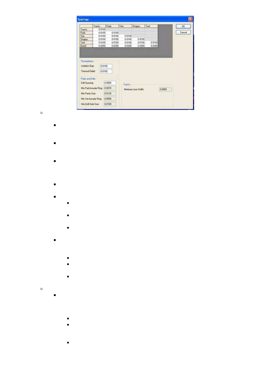
pour. The entire Shapes row must always be set to .010” at the minimum.
Board spacing is for the distance between the board rout line to copper features.
Board to copper spacings should all be set at .020” as the default in
Settings>Spacings.
For a routed or tab routed part, the settings could be set to .015” at the
minimum
For a scored part, the minimum allowable spacing from copper is .020” or
the designer risks exposed copper.
Drill spacing is to discover if drill holes are overlapping. This can happen when
another hole is placed inside a much bigger hole by accident and cannot be easily
viewable.
Most often this is seen when a via is accidentally placed inside another pad.
Click within the pad where you see the error and press <N> to cycle through
objects present at the point the cursor was clicked on.
If the via is not totally within the hole, the yellow pad of the via may be
visible.
Net Design Rules check for incomplete nets and also Dangling Traces.
Intentionally dangling tracks will produce an error message that will have to be
ignored. Simply note the number of errors so when the order is submitted, you
can see if the number of error has increased, indicating a new problem that must
be investigated before ordering.
Add a Track to fix the error, if the connection is confirmed to be needed.
Use Tools>Optimize Nets (or the hotkey <cntrl> <d>) to have the software
reconsider the netlist. Sometimes it will discover the connection to the net
exists in a different path than it was expecting, elsewhere in the board.
If there was no schematic created, there is no way to verify the integrity of
the design. A mistaken connection in the design can only be manually
Frequently Asked Questions
24 z 33
2010-07-12 18:29

confirmed (if that).
Overlapping copper pour areas can cause this. The system is arranged so
that overlapping polygons should never be necessary.
Isolated areas of a pour copper can cause this error. It is always best to
re-pour the pour copper and click on the Remove Islands option. Isolated
islands of copper behave as antennas.
Add Shape objects and filled polygons should only be used in areas too small
for an effective copper pour. It is preferred to use copper pour wherever
possible.
It is recommended to always ensure that the schematic is diligently
preserved as the point of all changes (using
Tools>PCBß>Schematic>Consistency check to forward differences from the
schematic to the PCB), to avoid the most serious of these types of errors,
even on the most simple board.
Manufacturing Design Rules cover many different areas of board design.
Minimum Line Width checks for tracks, draws and text using a smaller line .005”
Minimum annular ring check for:
.007” annular ring for component pads, minimum. That translates to .014”
over the hole size.
.005” annular ring for via pads, minimum. That translates into .010” over
the hole size.
Annular Ring Errors on mounting holes – The Plating checkbox in Properties
has been left on. If it is clicked off, the errors will not continue to show.
Minimum Drill checks for holes smaller than .008”.
Text outside board test is to flag text that is outside of the PCB and may be an
indication of an unplaced component.
Mirrored text check is to ensure that all solderside text is wrong-reading. Right-
reading text on the solderside will be wrong reading after manufacture of the part.
Minimum solder paste test should be turned off and ignored. Solder stencil
services vendors should have their own DFM tests that should perform for their
customer depending on many factors that are unknowable.
·
If there is doubt about the correct way to proceed, email your .pcb file and a brief
description of your situation to
layouthelp@4pcb.com
.
Arrays
Q:
What is an array (also referred to as a sub-panel, palette, etc)?
A: An array is putting multiple pieces of the same part number into frame to make small boards
more manufacturable for fabrication and also to reduce assembly costs for small boards. To
configure your design to be in an array, go to Settings>PCB Configuration and go to the Production
Page of that wizard. Click on the Array Checkbox in the middle of the page to open the array
options for editing. These are the various aspects of arrays:
The array size must be large enough to encompass all the individual pieces, the spacing
between those parts, and the border material that holds them together.
1.
The Borders are used for assembly operations to clamp onto securely without overlapping onto
the board and interfering with assembly.
2.
Tooling holes are also used for assembly operations to pin to. This is a more secure and
precise way to hole onto the board than clamping to the borders alone.
3.
Fiducials are used as optical targets for automated assembly. They are used to determine
precise board alignment.
4.
Scoring is a “v” grove cut into the top and bottom surfaces of an array configuration of
multiple PCB’s or a PCB with removable rails or frame. The cut depth is set such that the
material left is the lesser of .018” or 1/3 of the finished thickness. When this process is used
the printed circuit boards are typically set up side by side and end to end with no gap between
the edges. This results in the v-grove cutting into the area of the boards, so a .020” clearance
between the edge of the boards and any conductors is required.
5.
Frequently Asked Questions
25 z 33
2010-07-12 18:29

a.
When placing an order that requires scoring please indicate this requirement by
setting going to Settings>PCB Configuration.
b.
On the first page of that wizard, make the board Expand Design Requirement.
c.
On the Board Parameters page, click on the V-Score checkbox on the right.
Tab Routing for Arrays uses the router bit that cuts the board from the production panel to cut
slots between the individual images, leaving behind small “tabs” of unrouted material to keep
the array border and individual connected as one.
6.
When placing an order that requires scoring please indicate this requirement by setting
going to Settings>PCB Configuration.
a.
On the first page of that wizard, make the board Expand Design Requirement.
b.
On the Board Parameters page, click on the Tab Rout checkbox on the right.
c.
Q:
How do I make an array for a design?
A: Go to Settings>PCB Configuration. Go to the Production Page of that wizard. Click on the Array
Checkbox in the middle of the page.
1.
The optimum array size for efficient panel usage and lowest possible production cost is
10.8” x 7.8”. The goal is to come as close to that array size as possible without going
over.
2.
Here is an example of a PCB that is 3.5” x 2.2 to set up in an tab routed array:
·
To Determine the Array Width for PCB Artist, simply add up the x-axis dimensions.
For this board, the array width must be no less than 11.5”. Simply add up .4” + 3.5”
+ .1” + 3.5” + .1” + 3.5” + .4”.
·
The formula for the Array Width is the same, but for the Y axis dimensions. This
array width can be no less than 5.3”. That is .4” + 2.2” + .1” + 2.2” + .4”.
·
Borders to use:
o
The .4” border around the board is the minimum recommended for by
assembly companies. .5” is often preferred by assemblers.
o
A .2” border is the minimum manufacturable and cannot be changed, other
than to increase it. Assembly will be very difficult as only .1” will remain of
material. Tooling holes and fiducials cannot be added to this size.
o
To Add Tooling Holes and/or Fiducials to the array, you must have a minimum
of .4” border per side to the array.
·
Warning: PCB Artist currently allows a minimum of a .1” minimum border to
accommodate scored arrays and will allow an order of a tab rout with a .1” border.
However, this is not possible to produce and will cause the board to go on hold
Frequently Asked Questions
26 z 33
2010-07-12 18:29
pending customer authorization to increase to a .25” border (.2” at the minimum) and
approval of any associated changes to the cost of the order.
3.
Here is an example of a 3.5” x 2.2” board in a v-scored array:
·
The array width on this example can be no less than 11.3”. That is .4” + 3.5” +
3.5” + 3.5” + .4”.
·
The array height on this example can be no less than 5.2”. That is .4” + 2.2” +
2.2” + .4”.
·
There is no space between scored parts.
·
The .1” border is the minimum allowed cannot be changed, other than to make it
larger.
4.
Using the PCB Artist Array Dialog:
·
This example is using the tab rout.
·
Note that the Array Width and Array Height have the word “mils” at the end of
each field, indicating this board is set to mils, and the units entered must be in
mils, as seen in entering 11.5” as 11500.
·
Array Width is 11.5” (or 11,500 mils) as calculated above.
·
Array Height is 5.3” (or 5,300 mils) as calculated above.
·
Array up is the total number of parts in the array. In this case 6.
·
Note that the Quantity ordered is 18 parts. 18 individual parts which is 3 arrays.
o
The Quantity is for the total number of part numbers, NOT the number of
arrays. Arrays are never counted, only the individual parts which are
contained in the arrays.
o
The Quantity MUST be a multiple of the number of boards in the array. It
would give an error if I made the quantity 17 or 19. However, it would
accept 6, 12, 18, 24, etc.
Frequently Asked Questions
27 z 33
2010-07-12 18:29
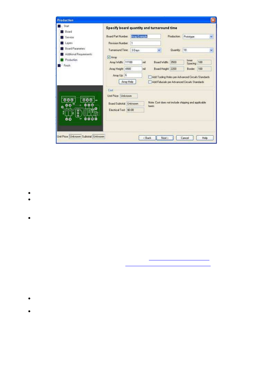
·
IMPORTANT – Basic Design Requirement orders are heavily discounted and do not
include v-scoring or tab routing. To get v-scoring or tab routing of an array, you must go
to Settings>PCB Configuration and set the board to Expand Design Requirement. Then
go to the Board Parameters page of that wizard and click on the checkbox for either
v-score or tab routing (or both).
Q:
Cant I just Copy and Paste to create the array and skip the other way?
A: Yes, but it is not recommended.
The schematic will now not be able to verify the design
The silkscreen reference designators auto-number, meaning that R1 on one part will not be
R23 on the second part pasted into the array and r41 on the next part pasted in. This will
reflect on the BOM, but basically very problematic in production assembly.
It is possible that in selecting the part across several layers that something may be missed
and not copied, which a schematic comparison will now be unable to catch.
Order Process Questions
Q:
How do I place an order?
A: This link takes you to instructions to the ordering a
Basic Design Requirement
order.
This link leads to instructions to place an
Expanded Design Requirement order
.
Q:
I clicked on Output>Submit order and it says that I have errors. What should I do?
A: The submit order process automatically runs the Design Rule Checks as part of Submit Order to
prevent the possibility of not running them before ordering and also to catch accidental edits that
the customer may not have been aware of.
If the Design Rule Checks have not been run, it is critical to check them before submitting the
order.
If the checks have been run and the number of errors is verified as per design, click to ignore
the errors and continue the order process.
Q:
The order process is looking for a .fab file. What is that?
A: The .fab file is a copy of the .pcb file you were working in when you hit the Place Order or Get
Quote button in the Submit Order process. It also serves as a “frozen” version of the exact file that
was ordered. If your order has issues and you need to send an edited file, do you edit in the .pcb
file and email the edited .pcb file to us. The .fab file will not be up to date and should only be used
when ordering online.
Frequently Asked Questions
28 z 33
2010-07-12 18:29

Installation
Q:
I am getting a windows warning saying "Due to a problem initializing a Microsoft OCX
control the grid cannot be displayed. This option has not been turned off in Preferences."
A: This is a known issue with some revisions of a Windows file. The fix depends on your operating
system. It is worth checking the date and version of the MSFLXGRD.OCX file on your system. There
are several different varieties of this OCX file in the field, some of them quite different in size and
date but showing the same version number.
Windows 7 and Vista 64:
Right click on Start/Accessories/Command Prompt and select Run As Administrator.
1.
Type: CD C:\Windows\Syswow64 <enter>
2.
Type: regsvr32 msflxgrd.ocx <enter>
3.
Type: exit <enter>
4.
Right click on the PCB Artist program icon and select Run As Administrator.
5.
From the PCB Artist main menu, go to File>Libraries
6.
Go to the Components Tab, select any component from the left-hand list, and click the
Edit button from the central list of buttons.
7.
Exit without saving and Close the PCB Artist program.
8.
Restart the PCB Artist normally.
9.
The key point here is that the "Run As Administrator" option is only available from
a menu or shortcut, so you need to launch the command prompt itself in this
mode by finding it on the Start menu.
Windows Vista 32:
Right click on Start/Accessories/Command Prompt and select Run As Administrator.
1.
Type: CD C:\Windows\System32 <enter>
2.
Type: regsvr32 msflxgrd.ocx <enter>
3.
Type: exit <enter>
4.
Right click on the PCB Artist program icon and select Run As Administrator.
5.
From the PCB Artist main menu, go to File>Libraries
6.
Go to the Components Tab, select any component from the left-hand list, and click the
Edit button from the central list of buttons.
7.
Exit without saving and Close the PCB Artist program.
8.
Restart the PCB Artist normally.
9.
The key point here is that the "Run As Administrator" option is only available from
a menu or shortcut, so you need to launch the command prompt itself in this
mode by finding it on the Start menu.
Windows XP/2000/ME/98/95:
From the Start menu, choose Run
1.
Type CMD (or on Windows 95/98/ME, type COMMAND), and click OK.
2.
Change directory to the folder containing your Windows system by typing:
CD \WINDOWS\SYSTEM32 <enter>
3.
On some systems your Windows files may be somewhere different, such as
\WINNT.
Use the Windows Search feature to locate the file if necessary.
Type: REGSVR32 MSFLXGRD.OCX <enter>.
4.
You should get a message telling you that the control has been registered.
5.
If you get an error message when running regsvr32, perhaps suggesting that although
the Flexgrid control is present but cannot be registered.
6.
Download the file from this
link
:
The file is compressed, unzip it and put it the unzipped file in CD \WINDOWS
\SYSTEM32.
Repeat the process starting at step 1, above.
Q:
Why do I get an error during installation saying I don’t have permissions to access
Frequently Asked Questions
29 z 33
2010-07-12 18:29

a file?
A: This is a very old Windows XP issue that has come up many times over the years.
v
WARNING: Advanced Circuits recommends seeking the aid of or retaining the services of
an experienced IT specialist to deal with this Windows issue. Customers performing this edit
do so at their own risk. It is possible to cause irreparable harm to the computer and lose all
files on the computer by performing any edits to the registry.
v
Before Editing:
Backup – This is the process for backing up the registry prior to editing it.
1.
Go to Run and type: Regedt32 <enter>
A.
Click on File>Export
B.
Save the file to a directory and make a note of its location.
C.
Restore - If the computer needs to be restored to its previous settings before the edit:
2.
A.
Run Regedt32 as was done in step a, above.
B.
Click on File>Import
C.
Locate the file from Step c above.
If the computer will not boot up:
3.
Press F8 while it is trying to boot.
A.
Choose the option to restore the last known good configuration.
B.
v
The Edit:
1.
Run regedt32.exe (It has to be regedt32 NOT regedit).
2.
Select the window HKEY_LOCAL_MACHINE ON LOCAL MACHINE.
3.
Select the SOFTWARE key.
4.
Click SECURITY (or PERMISSIONS) from the menu bar (under the "Edit" menu).
5.
Click PERMISSIONS.
6.
From the Security section, highlight USERS.
7.
Check the option FULL CONTROL.
8.
Click APPLY.
9.
Click the ADVANCED button.
10.
Highlight USERS from the Permission Entries section.
11.
Click VIEW/EDIT.
12.
From the permissions section, uncheck the DELETE option from the Allow column.
13.
Click OK.
14.
Click APPLY before continuing to the next step.
15.
Check the option RESET PERMISSIONS ON ALL CHILD OBJECTS AND ENABLE
PROPAGATION OF INHERITABLE PERMISSIONS.
16.
Click APPLY again.
17.
Click YES at the security dialog warning box.
18.
Click OK to the message about registry editor not being able to set permissions on
some keys.
19.
Click OK back at the access control settings for the SOFTWARE key.
20.
Click OK back at the permissions for SOFTWARE dialog.
Q:
I am having an installation problem that may be due to a proxy firewall. How can I
deal with this?
A: Please send an email describing the issue to
layouthelp@4pcb.com
.
Q:
I cannot find the directory where my design is stored. Where is it located?
A: There is a link to that directory in Start Menu>All Programs>Advanced Circuits>PCB Artist
Data.
In Windows XP and Windows 2000 the directory path is: C:\Documents and Settings\All
Users\Documents\PCB Artist. This directory structure allows PCB Artist files in that directory
to be stored in a way that allows all users of that computer to open and access the file.
In Windows 98 the directory path is: C:\Program Files\Advanced Circuits\PCB Artist.
To make files accessible to only the user, in the save dialog box navigate to My Documents
and save the files there. The files cannot be shared with all users from that directory.
PCB Artist will remember the last directory it saved a file to and will default to continue to
save there as is typical in many Windows applications.
Q:
Are other operating systems supported?
Frequently Asked Questions
30 z 33
2010-07-12 18:29

A: At this time only Windows systems from Windows 98 to Windows Vista are supported.
Some users are successfully using PCB Artist on the following operating systems with
emulation software:
Macintosh using Parallels
Macintosh using Virtual PC
Ubuntu Linux using Wine
Assembly
Q: How do I optimize the design for Advanced Circuits Assembly Services?
A: If you right click on a component and choose Properties from the right-click context menu. Then
click on the Values tab. From there you can enter values for the Manufacturer, Manufacturer Part
Number, Distributor, and Distributor Part Number.
If Advanced Circuits is providing a turnkey service of ordering the parts for an order, this
information will tremendously reduce the amount of time spent ordering the parts. This would
eliminate a large amount of redundant communication with the customer.
If the customer is providing the kit for the assembly, these populated values will make it
easier for the customer to have a comprehensive list of exactly what to order.
PCB Artist will create files that help to optimize the assembly process. These files are
embedded in the board design and only available for Advanced Circuits Assembly.
Do not put via holes inside surface mount lands, unless there is a critical electrical reason.
Always click on the Thermals Pads checkbox in the copper pour dialog when pouring copper.
Via holes can be directly connected to the plane and is a separate checkbox option.
Best Practices
v
The file with the Tilde “~” in the front of it is the security backup. This is not your
actual working file. The interval of how often it gets backed up is from Settings>PCB
Configuration. If you set that to zero, it will not perform a backup, which is not
recommended.
v
Do not use Delete to remove tracks for redrawing.
1.
Delete will remove the track and also its ratsnest connection. Delete is intended to
completely remove the connection from the netlist.
2.
To Remove the track, but not the connection:
·
Select a segment of the track
·
Right click on it and choose Nets>Unroute Track Segments (or Unroute Track
Path) from the right-click context menu. The track will be replaced with an
unrouted ratsnest connection.
v
It is not recommended to use Undo to remove the results of the autorouter. Use
Tools>Unrout Nets>All Nets.
v
Be careful when joining nets.
1.
A warning will appear such as this:
2.
Be sure that the new net created by both is the correct one. This depends upon
which net you were drawing with. Cancel and redraw your connect from the other net
to make the resultant net the desired one.
Frequently Asked Questions
31 z 33
2010-07-12 18:29

3.
Once the net is joined, it cannot be split. The smaller net must be deleted and
redrawn.
v
Avoid overlapping copper pours where possible.
1.
Overlapping copper pours confuse the netlist.
2.
If click down on the wheel of a wheel mouse, it will pan across the screen while
dragging different types of draws including polygons. This makes drawing overlapping
polygons unnecessary.
v
Do not use copper pours for contact lands.
1.
They will not have a soldermask clearance. They will be covered by soldermask,
which is very hard to scrape off of the contact.
2.
Options:
·
Reconstruct them as surface mounts.
·
Create a clearance of a filled rectangle or polygon on the soldermask layer.
v
If your surface mount is colored gray, it requires a crucial edit.
1.
Go into the Properties of the object and change them from layer [All] to layer [Top].
2.
If the surface mount is part of a component, the edit must be done in the PCB
Symbol editor.
3.
This assumes that the default color settings are being used.
v
Make sure your power and ground nets are properly defined in Settings>Nets as
Power or Ground in the Class Column.
1.
Power and ground traces usually need to be thicker than signal traces. All nets are
classified as signal until the designer changes them to a Power or Ground Class.
v
Plane layers cannot have draws or tracks on them.
1.
They cannot have even one trace added to them.
2.
If tracks must be drawn on them, change the layer to a Signal in Settings>PCB
Configuration on the Layers page of that wizard and use Pour Copper to add the plane
areas.
v
Always create a new library for any parts you create or modify.
1.
If a future version of PCB Artist needs a complete installation, any existing
pre-packaged libraries are automatically overwritten and all parts will be lost.
2.
All part creation documentation in this document describes the process of making a
new library for your part.
v
In Settings>Spacings, never change the Board row to less than .020” or the Shape
row to less than .010”.
1.
Those settings are not only for Design Rule Checks, but also provide rules for how
copper pours are created.
v
Do not create parts with the same name as any other part in any other library.
1.
The system acquires parts in a hierarchy of libraries that are searched when symbols
are updated in the PCB or Schematic. If the other part with same name in the other
library are located first, it will now be associated to that symbol.
v
Do not add Vias inside Surface Mount Lands.
Many designers add vias inside surface mount lands as a way of conserving space in a
design. This creates greater difficulty and lower quality solder joints in assembly.
This practice is not recommended unless absolutely necessary for electrical purposes.
v
Always use Thermal Pads in Copper Pours for component holes.
Regardless of heat sink needs, always use thermal pads in copper pours for
component pads. Thermals pads are not necessary on vias. Directly connecting lands
to the planes will cause assembly problems are poor quality solder joints.
v
Preventing accidental edits.
1.
Making layers or object types unselectable is possible from View>Colors. Go to the
Layered Items tab.
Frequently Asked Questions
32 z 33
2010-07-12 18:29

·
The Selectable row locks objects by changing the cell from Yes to No with a
double click of the mouse button.
·
The Selectable column locks objects for specific layers by double clicking the
cell from Yes to No.
·
Individual objects can be locked from editing by selecting that object, right-
clicking on it, and choosing Fix Item. This will prompt a dialog box asking for
confirmation if an edit is attempted on a specific object.
If you have a new question, please don’t hesitate to send it to
Layouthelp@4pcb.com
Frequently Asked Questions
33 z 33
2010-07-12 18:29
Wyszukiwarka
Podobne podstrony:
frequently asked questions?out?mons
A Course in Miracles Frequently Asked Questions Doug Thompson (Share Me) (ebook)
Frequently asked QUESTIONS about DOLBY DIGITAL
Catholic hospitals Frequently asked questions
Frequently asked Qusetions Anorexia Nervosa
Pec 12 frequent questions Sensor Cleaning for DSLR and Mirrorless Cameras
Question
Frequenzimetro eng 2003
English, Intermediate Grammar Questions answers
Dealing with competency?sed questions
Study Questions for Frankenstein odpowiedzi
Induction Generator Based System Providing Regulated Voltage With Constant Frequency
501 Sentence Completion Questions
101 veterinary technician questions answered
IINS PRACTICE QUESTIONS
Intermediate Short Stories with Questions, Driving Directions
Exam questions sample1
Adverbs of frequency
Confusion Inducing Questions
więcej podobnych podstron