tl062dil
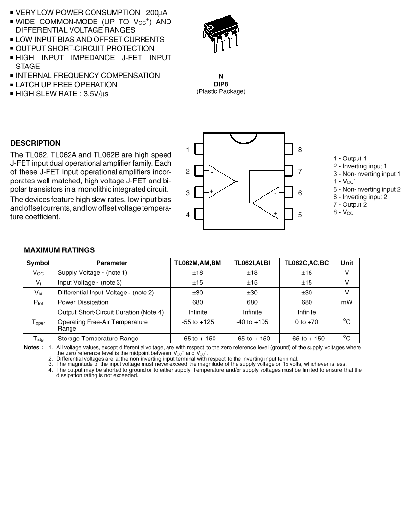

N
DIP8
(Plastic Package)
1 - Output 1
2 - Irwerting input 1
3 - Non-inverting input 1
4 - Vcc
5 - Non-inverting input 2
6 - lnverting input 2
7 - Output 2
8 - VCc+
■ VERY LOW POWER CONSUMPTION : 200uA
■ WIDE COMMON-MODE (UP TO Vcc+) AND DIFFERENTIAL VOLTAGE RANGES
■ LOW INPUT BIAS AND OFFSET CURRENTS
■ OUTPUT SHORT-CIRCUIT PROTECTION ■HIGH INPUT IMPEDANCE J-FET INPUT
STAGE
■ INTERNAL FREOUENCY COMPENSATION
■ LATCH UP FREE OPERATION
■ HIGH SLEW RATĘ : 3.5V/ps
DESCRIPTION
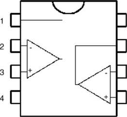
The TL062, TL062A and TL062B are high speed J-FET input dual operational amplifier family. Each of these J-FET input operational amplifiers incor-porates well matched, high voltage J-FET and bi-polar transistors in a monolithic integrated Circuit. The devicesfeature high siew rates, Iow input bias and offsetcurrents, and Iow offset voltage temperaturę coefficient.
MAXIMUM RATINGS
|
Symbol |
Parameter |
TL062M.AM,BM |
TL062I,AI,BI |
TL062C,AC,BC |
Unit |
|
Vcc |
Supply Voltage - (notę 1) |
±18 |
±18 |
±18 |
V |
|
Vi |
Input Voltage - (notę 3) |
±15 |
±15 |
±15 |
V |
|
V* |
Differential Input Voltage- (notę 2) |
±30 |
±30 |
±30 |
V |
|
Ftot |
Power Dissipation |
680 |
680 |
680 |
mW |
|
Output Short-Circuit Duration (Notę 4) |
Infinite |
Infinite |
Infinite | ||
|
Toper |
Operating Free-Air Temperature Rangę |
-55 to+125 |
-40 to+105 |
0 to +70 |
°C |
|
Tstg |
Storage Temperaturę Rangę |
- 65 to + 150 |
- 65 to + 150 |
- 65 to + 150 |
°c |
Notes : 1. Ali voltage values, except ditferential voltage. are v/ith respect to the zero reference level (ground) of the supply voltages where
the zero reference levei is the midpointbetween Vcc* and Vcc •
2. Differential voltages are at the non-inverting input terminal with respect to the inverting input terminal.
3. The magnitude of the input vołtage must never exceed the magnitude of the supply voltage or 15 volts, whichever is less.
4. The output may be shorted to ground or to either supply. Temperaturo andfor suppły voltages must be limited to ensure that the dissipation rating is not exceeded.
Wyszukiwarka
Podobne podstrony:
tl431 LP SUFFIX Plastic Package Case 29-04 Pin 1 - Reference 2 - Anodę 3
tl431 LP SUFFIX Plastic Package Case 29-04 Pin 1 - Reference 2 - Anodę 3
Slajd28 (127) System BIOS(Basic Input Output System) •zbiór procedur(funkcji) sterujących
img67 A 1-??????? +12? 1 -Input-L 1-Speaker FL+ 1-Remote Output 1 2-Input-R 2-Speaker
MIMOOTA performance testing Multiple input multiple output (MIMO) techniques have been introduced to
New test methods for MIMO OTA measurements Currently, OTA performance tests for single input si
IMG 95 (4) ZAGADNIENIA FIZYKI WSPÓŁCZESNEJWzbogacenie uranu — metoda dyfuzji gazowej Bnrlch*d Input
BIOS (akronim ang. Basic Input/Output System - podstawowy system wejścia-wyjścia) - zapisany w pamię
- wprowadzenie do architektury komputera. - Basic Input Output S
NI - Normal Input NO - Normal Output SI - Serial Input SO - Serial OutputBSC - Boundary Scan Celi OB
Standardy napięciowe Input/Output Standard V
new prox amp(1) J1 RF Input +20 dBm Max. g-E C6 ± C8 IC1 RF Micro Devlces RF2126 "^7 C5 J2 RF O
INPUT (balancod)OUTPUT (balancod) UBWOOFE (balancod)LEVEL HIGH CUT(Hz) ii., .‘,-a aMiK *Sk Of
więcej podobnych podstron