37496 Proc
+5V
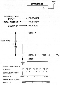
AT89S8252
'cc
INSTRUCTION
INPUT -H
DATA OUTPUT -4-
CLOCK IN -H
4-24 MHz
□
>
P1.SWOSI
PI.&WISO
P1.7/SCK
XTAL 2
XTAL 1 QND
RST
SERIAL CLCCK IMPUł 5CWI.7 __
SERIAL DATA INPUT
MOSMP1.S _ !US0i _ SERIAL DATA OUTPUT j UISO'Pl.6
TJIJIJTJTJTJTJI
i o
r c t 4 3 2
* I I I
TtSBl
Wyszukiwarka
Podobne podstrony:
84 M. Suwała Tabela 2 Table 2 Dane wyjściowe do obliczenia kosztów Input data for cost
FC1 : SEW Inverter Controled by 3 Process Data Words. Reading Process Input Data and Writing Process
PotentiometerLED LED GND PWM (analog output) pin*O-W—AV r (200 ohm) +5V potentiometer GND analog inp
004 (42) Plik Widok Narzędzia Rozwiązania Okno Pomoc W3 D OrM Sta X Hi ® o Eksplorator iii Input Dat
• SISD (Single Instruclion Single Data) Skalarne • SLMD (Single
DSCN5413 LI cache organ ization Split instruction and data caches Split instruction and data caches
MIMOOTA performance testing Multiple input multiple output (MIMO) techniques have been introduced to
New test methods for MIMO OTA measurements Currently, OTA performance tests for single input si
Instrukcje warunkowe UNIX (2) Instrukcja warunkowa case: case zmienna in "wzorzecl") pol
milo 01 02 Preliminary Instructions m inaking up thc followiug instructions for thc diffcrcnt excrci
INPUT (balancod)OUTPUT (balancod) UBWOOFE (balancod)LEVEL HIGH CUT(Hz) ii., .‘,-a aMiK *Sk Of
IMGY44 (3) Data ** W. Zoi°? iml« • i»n**iWu» I Vfana •°»=l Molika —*HH)43~ 465 ^oboVa Yolaion I
więcej podobnych podstron