Analog Dialogue 34-2 (2000)
1
1
Edwin Goldberg and Jules Lehmann, U. S. Patent 2,684,999: Stabilized dc
amplifier.
Demystifying Auto-Zero
Amplifiers—Part 1
They essentially eliminate offset, drift,
and 1/f noise. How do they work?
Is there a downside?
by Eric Nolan
INTRODUCTION
Whenever the subject of auto-zero or chopper-stabilized amplifiers
comes up, the inevitable first question is “How do they really work?”
Beyond curiosity about the devices’ inner workings, the real
question in most engineers’ minds is, perhaps, “The dc precision
looks incredible, but what kind of weird behavior am I going to
have to live with if I use one of these in my circuit; and how can I
design around the problems?” Part 1 of this article will attempt to
answer both questions. In Part 2, to appear in the next issue, some
very popular and timely applications will be mentioned to illustrate
the significant advantages, as well as some of the drawbacks, of
these parts.
CHOPPER AMPLIFIERS—HOW THEY WORK
The first chopper amplifiers were invented more than 50 years
ago to combat the drift of dc amplifiers by converting the dc voltage
to an ac signal. Initial implementations used switched ac coupling
of the input signal and synchronous demodulation of the ac signal
to re-establish the dc signal at the output. These amplifiers had
limited bandwidth and required post-filtering to remove the large
ripple voltages generated by the chopping action.
Chopper-stabilized amplifiers solved the bandwidth limitations by
using the chopper amplifier to stabilize a conventional wide-band
amplifier that remained in the signal path
1
. Early chopper-stabilized
designs were only capable of inverting operation, since the
stabilizing amplifier’s output was connected directly to the non-
inverting input of the wide-band differential amplifier. Modern
IC “chopper” amplifiers actually employ an auto-zero approach
using a two-or-more-stage composite amplifier structure similar
to the chopper-stabilized scheme. The difference is that the
stabilizing amplifier signals are connected to the wide-band or main
amplifier through an additional “nulling” input terminal, rather
than one of the differential inputs. Higher-frequency signals bypass
the nulling stage by direct connection to the main amplifier or
through the use of feed-forward techniques, maintaining a stable
zero in wide-bandwidth operation.
This technique thus combines dc stability and good frequency
response with the accessibility of both inverting and noninverting
configurations. However, it may produce interfering signals
consisting of high levels of digital switching “noise” that limit the
usefulness of the wider available bandwidth. It also causes
intermodulation distortion (IMD), which looks like aliasing between
the clock signal and the input signal, producing error signals at
the sum and difference frequencies. More about that later.
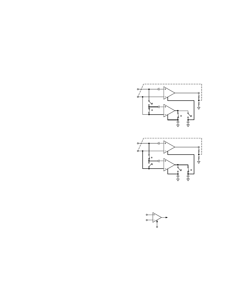
Auto-Zero Amplifier Principle
Auto-zero amplifiers typically operate in two phases per clock cycle,
illustrated in Figures 1a and 1b. The simplified circuit shows a
nulling amplifier (A
A
), a main (wide-band) amplifier (A
B
), storage
capacitors (C
M1
and C
M2
), and switches for the inputs and storage
capacitors. The combined amplifier is shown in a typical op-amp
gain configuration.
In Phase A, the auto-zero phase (Figure 1a), the input signal is
applied to the main amplifier (A
B
) alone; the main amplifier’s
nulling input is supplied by the voltage stored on capacitor C
M2
;
and the nulling amplifier (A
A
) auto-zeros itself, applying its nulling
voltage to C
M1
. In Phase B, with its nulling voltage furnished by
C
M1
, the nulling amplifier amplifies the input difference voltage
applied to the main amplifier and applies the amplified voltage to
the nulling input of the main amplifier and C
M2
.
V
OSB
V
NB
V
OSA
V
NA
A
B
C
M1
C
M2
V
O
EXTERNAL
FEEDBACK
A
B
V
I+
V
I–
A
B
A
A
a. Auto-Zero Phase A: null amplifier nulls its own offset.
V
OSB
V
NB
V
OSA
V
NA
A
B
C
M1
C
M2
V
O
EXTERNAL
FEEDBACK
A
B
V
I+
V
I–
A
B
A
A
b. Output Phase B: null amplifier nulls the main amplifier
offset.
Figure 1. Switch settings in the auto-zero amplifier.
Both amplifiers use the trimmable op-amp model (Figure 2), with
differential inputs and an offset-trim input.
V
I+
V
I–
V
N
V
O
A
B
V
O
= A(V
I+
–V
I–
) +BV
N
A = DIFFERENTIAL GAIN
B = TRIM GAIN
Figure 2. Trimmable op amp model.
In the nulling phase (Phase A—Figure 1a), the inputs of the nulling
amp are shorted together and to the inverting input terminal
(common-mode input voltage). The nulling amplifier nulls its own
inherent offset voltage by feeding back to its nulling terminal
whatever opposing voltage is required to make the product of that

2
Analog Dialogue 34-2 (2000)
voltage and the incremental gain of the nulling input approximately
equal to A
A
’s input offset (V
OS
). The nulling voltage is also
impressed on C
M1
. Meanwhile, the main amplifier is behaving like
a normal op amp. Its nulling voltage is being furnished by the
voltage stored on C
M2
.
During the output phase (Phase B—Figure 1b) the inputs of the
nulling amplifier are connected to the input terminals of the main
amplifier. C
M1
is now continuing to furnish the nulling amplifier’s
required offset correction voltage. The difference input signal is
amplified by the nulling amplifier and is further amplified by the
incremental gain of the main amplifier’s nulling input circuitry. It
is also directly amplified by the gain of the main amplifier itself
(A
B
). The op amp feedback will cause the output voltage of the
nulling amplifier to be whatever voltage is necessary at the main
amplifier’s nulling input to bring the main amplifier’s input
difference voltage to near-null. Amplifier A
A
’s output is also
impressed on storage capacitor C
M2
, which will hold that required
voltage during the next Phase A.
The total open-loop amplifier dc gain is approximately equal to
the product of the nulling amplifier gain and the wide-band
amplifier nulling terminal gain. The total effective offset voltage is
approximately equal to the sum of the main-amplifier and nulling-
amplifier offset voltages, divided by the gain at the main amplifier
nulling terminal. Very high gain at this terminal results in very low
effective offset voltage for the whole amplifier.
As the cycle returns to the nulling phase, the stored voltage on
C
M2
continues to effectively correct the dc offset of the main
amplifier. The cycle from nulling to output phase is repeated
continuously at a rate set by the internal clock and logic circuits.
(For detailed information on the auto-zero amplifier theory of
operation see the data sheets for the AD8551/AD8552/AD8554
or AD857x amplifiers).
Auto-Zero Amplifier Characteristics
Now that we’ve seen how the amplifier works, let’s examine its
behavior in relation to that of a “normal” amplifier. First, please
note that a commonly heard myth about auto-zero amplifiers is
untrue: the gain-bandwidth product of the overall amplifier is not
related to the chopping clock frequency. While chopping clock
frequencies are typically between a few hundred Hz and several
kHz, the gain bandwidth product and unity-gain bandwidth of
many recent auto-zero amplifiers is 1 MHz–3 MHz—and can be
even higher.
A number of highly desirable characteristics can be easily inferred
from the operating description: dc open-loop voltage gain, the
product of the gains of two amplifiers, is very large, typically more
than 10 million, or 140 dB. The offset voltage is very low due to
the effect of the large nulling-terminal gain on the raw amplifier
offsets. Typical offset voltages for auto-zero amplifiers are in the
range of one microvolt. The low effective offset voltage also impacts
parameters related to dc changes in offset voltage—dc CMR and
PSR, which typically exceed 140 dB. Since the offset voltage is
continuously “corrected,” the shift in offset over time is vanishingly
small, only 40 nV–50 nV per month. The same is true of
temperature effects. The offset temperature coefficient of a well-
designed amplifier of this type is only a few nanovolts per
°C!
A less obvious consequence for the amplifier’s operation is the
low-frequency “1/f noise” characteristic. In “normal” amplifiers,
the input voltage noise spectral density increases exponentially
inversely with frequency below a “corner” frequency, which may
be anywhere from a few Hz to several hundred Hz. This low-
frequency noise looks like an offset error to the auto-correction
circuitry of the chopper-stabilized or auto-zero amplifier. The
auto-correction action becomes more efficient as the frequency
approaches dc. As a result of the high-speed chopper action in
an auto-zero amplifier, the low-frequency noise is relatively flat
down to dc (no 1/f noise!). This lack of 1/f noise can be a big
advantage in low-frequency applications where long sampling
intervals are common.
Because these devices have MOS inputs, bias currents, as well as
current noise, are very low. However, for the same reason, wide-
band voltage noise performance is usually modest. The MOS inputs
tend to be noisy, especially when compared to precision bipolar-
processed amplifiers, which use large input devices to improve
matching and often have generous input-stage tail currents. Analog
Devices AD855x amplifiers have about one-half the noise of most
competitive parts. There is room for improvement, however, and
several manufacturers (including ADI) have announced plans for
lower-noise auto-zero amplifiers in the future.
Charge injection [capacitive coupling of switch-drive voltage into
the capacitors] occurs as the chopping switches open and close.
This, and other switching effects, generates both voltage and
current “noise” transients at the chopping clock frequency and its
harmonics. These noise artifacts are large compared to the wide-
band noise floor of the amplifier; they can be a significant error
source if they fall within the frequency band of interest for the
signal path. Even worse, this switching causes intermodulation
distortion of the output signal, generating additional error signals
at sum and difference frequencies. If you are familiar with sampled-
data systems, this will look much like aliasing between the input
signal and the clock signal with its harmonics. In reality, small
differences between the gain-bandwidth of the amplifier in the
nulling phase and that in the output phase cause the closed-loop
gain to alternate between slightly different values at the clock
frequency. The magnitude of the IMD is dependent on the internal
matching and does not relate to the magnitude of the clock “noise.”
The IMD and harmonic distortion products typically add up to
about –100 dB to –130 dB plus the closed-loop gain (in dB), in
relation to the input signal. You will see below that simple circuit
techniques can limit the effects of both IMD and clock noise
when they are out of band.
Some recent auto-zero amplifier designs with novel clocking
schemes, including the AD857x family from Analog Devices, have
managed to tame this behavior to a large degree. The devices in
this family avoid the problems caused by a single clocking frequency
by employing a (patented) spread-spectrum clocking technique,
resulting in essentially pseudorandom chopper-related noise. Since
there is no longer a peak at a single frequency in either the intrinsic
switching noise or “aliased” signals, these devices can be used at
signal bandwidths beyond the nominal chopping frequency without
a large error signal showing up in-band. Such amplifiers are much
more useful for signal bandwidths above a few kHz.

Analog Dialogue 34-2 (2000)
3
Some recent devices have used somewhat higher chopping
frequency, which can also extend the useful bandwidth. However,
this approach can degrade V
OS
performance and increase the input
bias current (see below regarding charge injection effects); the
design trade-offs must be carefully weighed. Extreme care in both
design and layout can help minimize the switching transients.
As mentioned above, virtually all monolithic auto-zero amplifiers
have MOS input stages, tending to result in quite low input bias
currents. This is a very desirable feature if large source impedances
are present. However, charge injection produces some unexpected
effects on the input bias-current behavior.
At low temperatures, gate leakage and input-protection-diode
leakage are very low, so the dominant input bias-current source is
charge injection on the input MOSFETs and switch transistors.
The charge injection is in opposing directions on the inverting
and noninverting inputs, so the input bias currents have opposing
polarities. As a result, the input offset current is larger than the input
bias current. Fortunately, the bias current due to charge injection
is quite small, in the range of 10 pA–20 pA, and it is relatively
insensitive to common-mode voltage.
As device temperature rises above 40
°C to 50°C, the reverse leakage
current of the input protection diodes becomes dominant; and
input bias current rises rapidly with temperature (leakage currents
approximately double per 10
°C increase). The leakage currents
have the same polarity at each input, so at these elevated
temperatures the input offset current is smaller than the input
bias current. Input bias current in this temperature range is strongly
dependent on input common-mode voltage, because the reverse
bias voltage on the protection diodes changes with common-mode
voltage. In circuits with protection diodes connected to both supply
rails the bias current polarity changes as the common-mode voltage
swings over the supply-voltage range.
Due to the presence of storage capacitors, many auto-zero
amplifiers require a long time to recover from output saturation
(commonly referred to as overload recovery). This is especially
true for circuits using external capacitors. Newer designs using
internal capacitors recover faster, but still take milliseconds to
recover. The AD855x and AD857x families recover even faster—
at about the same rate as “normal” amplifiers—taking less than
100
µs. This comparison also holds true for turn-on settling time.
Finally, as a consequence of the complex additional circuitry
required for the auto-correction function, auto-zero amplifiers
require more quiescent current for the same level of ac
performance (bandwidth, slew rate, voltage noise and settling
time) than do comparable nonchopped amplifiers. Even the
lowest power auto-zero amplifiers require hundreds of
microamperes of quiescent current; and they have a very modest
200-kHz bandwidth with broadband noise nearly 150 nV/
√Hz
at 1 kHz. In contrast, some standard CMOS and bipolar
amplifiers offer about the same bandwidth, with lower noise,
on less than 10
µA of quiescent current.
APPLICATIONS
Notwithstanding all of the differences noted above, applying
auto-zero amplifiers really isn’t much different from applying
any operational amplifier. In the next issue, Part 2 of this article
will discuss application considerations and provide examples
of applications in current shunts, pressure sensors and other
strain bridges, infrared (thermopile) sensors, and precision
voltage references.
Wyszukiwarka
Podobne podstrony:
The Definite or Zero Article Exercise at Auto
Gdzie kupić używane auto
Materiały nieżelazne Tworzywa sztuczne Przetwórstwo Auto Expert
AUTO, DO ĆWICZEŃ DŹWIĘKONAŚLADOWCZYCH
sprawko z lab3 z auto by pawelekm
Maly Modelarz 1976 08] Auto F1 & GT(GT Only)
auto data 2010pl 789069998 ID6c9Y
kurs ZERO OSN wiczenie 01
kurs ZERO OSN wiczenie 05
original c68 retail diy auto diagnostic tool manual
Chcesz kupić używane auto sprawdź jego historię
ogolne warunki ubezpieczenia ptu auto assistance podstawowy
Odlewnictwo Auto Expert(1)
Biznes Plan - Auto-Plus, Prace dyplomowe, Biznes Plany
SWIAT~42, Akademia Morska -materiały mechaniczne, szkoła, Mega Szkoła, szkola1, III, AUTO
(Nie)bezpieczne auto, MEDYCYNA, RATOWNICTWO MEDYCZNE, BLS, RKO
więcej podobnych podstron