IEEE TRANSACTIONS ON CIRCUITS AND SYSTEMS—I: REGULAR PAPERS, VOL. 52, NO. 10, OCTOBER 2005
2219
A ZVS PWM Inverter With Active Voltage Clamping
Using the Reverse Recovery Energy of the Diodes
Marcello Mezaroba, Denizar Cruz Martins, and Ivo Barbi
Abstract—This paper presents a zero-voltage-switching (ZVS)
pulsewidth modulated inverter with active voltage clamping using
only a single auxiliary switch. The structure is particularly simple
and robust. It is very attractive for single-phase high-power appli-
cations. Switching losses are reduced due to implementation of the
simple active snubber circuit that provides ZVS conditions for all
switches, including the auxiliary one. Its main features are: simple
modulation strategy, robustness, low weight and volume, low har-
monic distortion of the output current and high efficiency. The
principle of operation for steady-state conditions, mathematical
analysis and experimental results from a laboratory prototype are
presented.
Index Terms—Active clamping, inverters, soft commutation.
I. I
NTRODUCTION
M
UCH effort has been exerted by researchers all over
the world in an attempt to reduce harmonic distortion
and audible noise in the output of inverters. Their objectives
have been attained through an increase in inverter commutation
frequencies and an appropriate modulation strategy. These
measures have provided some benefits, such as a reduction in
the weight and volume of the magnetic elements. However,
they have caused some difficulties due to the high commutation
losses in the switches and the appearance of electromagnetic
interference. These factors occur mainly in inverter topologies
that use the bridge inverter configuration. At the moment that
the main switch turns on, the anti-parallel diode of the bridge
complementary switch begins its reverse recovery phase.
During this stage, the switches are submitted to a high current
ramp rate
and a high peak-reverse recovery current
.
Both contribute significantly to increasing the commutation
losses and produce electromagnetic interference.
To solve this problem, diverse works have been developed
by the scientific community in recent years and can be divided
into two groups: passive techniques and active techniques.
The passive techniques are characterized by the absence of
controlled switches in the switching aid circuit, while the active
techniques are characterized by circuits that use controlled
switches. Among the passive solutions, perhaps the most
Manuscript received May 28, 2004; revised September 15, 2004. This paper
was recommended by Associate Editor A. Ioinovici.
M. Mezaroba is with the Power Electronics Laboratory (LEPO), the State
University of Santa Catarina (UDES), 89223-100 Joinville, SC, Brazil (e-mail:
mezaroba@joinville.udesc.br).
D. C. Martins and I. Barbi are with the Power Electronics Institute (INEP),
the Federal University of Santa Catarina (UFSC), 88040-970 Florianópolis, SC,
Brazil (e-mail: denizar@inep.ufsc.br; ivobarbi@inep.ufsc.br).
Digital Object Identifier 10.1109/TCSI.2005.852914
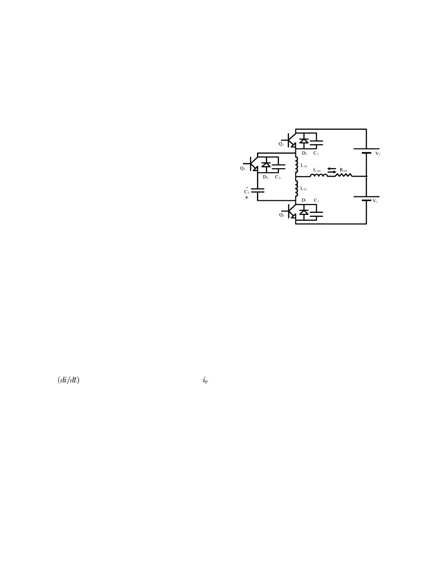
Fig. 1.
Proposed circuit.
widely known is the Undeland snubber [1]. This snubber pro-
vides good performance in the majority of its applications, but
is not capable of regenerating the energy lost in switching. To
try to minimize these losses, some works have considered mod-
ifications to the Undeland snubber, aiming at the regeneration
of the energy lost in switching [2]–[4] and [5]. The active solu-
tions are already distinguished by the use of controlled switches
to obtain soft commutation. The main ones are those that use
conventional pulsewidth modulation (PWM), without the need
for special control circuits. One of these works is the auxiliary
resonant auxiliary resonant diode pole inverter (ARDPI) [6].
This topology matches the use of PWM modulation, with the
soft switching attained through a relatively simple circuit. On
the other hand, it needs a high current circulating in the circuit,
about 2.5 times the load current, raising the current stress in
the switches. A topology very similar to the previous one is the
auxiliary resonant pole inverter (ARPI) [7]. Theoretically, this
circuit reduces the current levels necessary for switching, but
it involves a complex control strategy. Another circuit found
in literature is the auxiliary resonant commutated pole inverter
(ARCPI) [8], [9], and [10]. This inverter has auxiliary switches
that are only turned on when the load current is not sufficient to
effect the soft switching, causing the control circuit to become
very complex and dependent on the sensors.
Recently, some research was carried out using the reverse re-
covery energy from the diodes to obtain soft commutation in the
switches of the pre-regulated rectifiers with high power factor
[11] and [12].
In this paper, a zero-voltage-switching (ZVS) PWM inverter
with voltage clamping across the switches, using only a single
auxiliary switch, is presented. The proposed structure uses the
diode reverse recovery energy technique to obtain soft commu-
tation in all switches, such as the rectifier shown in [12].
1057-7122/$20.00 © 2005 IEEE
2220
IEEE TRANSACTIONS ON CIRCUITS AND SYSTEMS—I: REGULAR PAPERS, VOL. 52, NO. 10, OCTOBER 2005
Fig. 2.
Operation stages. (a) First state (t0-t1). (b) (b) Second stage (t1-t2). (c) Third stage (t2-t3). (d) Fourth stage (t3-t4). (e) Fifth stage (t4-t5). (f) Sixth stage
(t5-t6). (g) Seventh stage (t6-t7). (h) Eighth stage (t7-t8). (i) Ninth stage (t8-t0).
II. P
ROPOSED
C
IRCUIT
The proposed circuit is shown in Fig. 1. It presents a
half-bridge inverter configuration, where
are the main
switches. The snubber circuit is formed by one switch
,
one small center-tapped inductor
and one capacitor
.
, and
are the commutation capacitors. Capacitor
is responsible for the storage of the diode reverse recovery
energy and for the clamping of the voltage across the switches.
Inductors
and
are responsible for the control of the
during the diode reverse recovery time.
III. O
PERATION
S
TAGES
(
FOR
F
IRST
H
ALF
-C
YCLE
)
To simplify the analysis, the following assumptions are
made: the circuit operates in steady state; the components are
considered ideal; the voltage across capacitor
and the cur-
rent through the output inductor
are considered constant
during the switching period.
In the following paragraphs, the operation stage (Fig. 2) of
the first positive half-cycle of the output current is described in
detail.
First Stage (t0–t1): At t0, switch
is turned on. During
this interval, the output current,
, is delivering energy to
source
via diode
. At the same time, additional current
circulates through the mesh, formed by
, and
. At the end of this stage, the current through inductor
reaches its maximum value,
(Fig. 3)
(1)
(2)
(3)
(4)
(5)
This stage was chosen to initiate the converter analysis because
it precedes the commutation process of the main switch,
,
during the half-cycle of operation. At time t0 current
becomes positive and increases linearly. At the end of the
first stage this current is responsible for the soft commutation
process of
.
Second Stage (t1-t2): This stage starts when auxiliary switch
is blocked. Current
charges capacitor
from zero
to
, and discharges
from
to zero.
. During this stage the current,
, circulates through
the intrinsic capacitor of switch
(6)
where
is the maximum current through
. Thus
(7)
MEZAROBA et al.: ZVS PWM INVERTER WITH ACTIVE VOLTAGE CLAMPING
2221
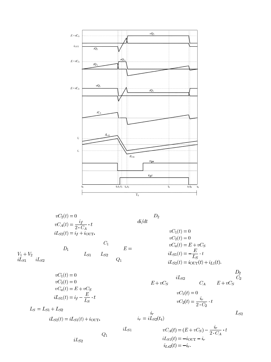
Fig. 3.
Main waveforms.
(8)
(9)
(10)
Third Stage (t2-t3): At t2, the voltage across
reaches zero
and is clamped by diode
. At this moment, the voltage
is applied across inductors
and
and currents
and
decrease linearly. In this stage, switch
must
be turned on
(11)
(12)
(13)
(14)
where
.
(15)
Fourth Stage (t3-t4): This stage begins when current
inverts its direction and flows through switch
. The turn-on
occurs at zero voltage. Current
continues to decrease until
inverting its direction, which begins the reverse recovery phase
of diode
. The auxiliary inductors limit the reverse recovery
(16)
(17)
(18)
(19)
(20)
Fifth Stage (t4-t5): This stage starts when diode
stops
conducting. Current
begins charging capacitor
from
zero to
and discharging
from
to zero
(21)
(22)
where
is the maximum negative current through
. So,
(23)
(24)
(25)
2222
IEEE TRANSACTIONS ON CIRCUITS AND SYSTEMS—I: REGULAR PAPERS, VOL. 52, NO. 10, OCTOBER 2005
Sixth Stage (t5-t6): At t5, the voltage across capacitor
reaches zero and is clamped by diode
. Currents
and
increase, due to the application of voltage
across in-
ductors
and
. In this stage, switch
must be turned
on. It is important to emphasize that the drive time of switch
is estimated previously and kept constant during the en-
tire inverter operation range. So, the use of current sensor is not
necessary
(26)
(27)
(28)
(29)
(30)
Seventh Stage (t6-t7): This stage begins when current
changes its direction and flows through switch
. Current
continues to increase linearly
(31)
(32)
(33)
(34)
(35)
Eighth Stage (t7-t8): During this stage, switch
is
blocked and the current through
inverts its direction and
flows through diode
. Capacitor
charges itself from zero
to
and capacitor
discharges from
to zero
(36)
(37)
(38)
(39)
(40)
(41)
Ninth Stage (t8-t0): This stage begins when the voltage
across capacitor
reaches zero and is clamped by diode
.
Current
continues to increase. This stage finishes when
inverts its direction and flows through auxiliary switch
, restarting the first operation stage
(42)
(43)
(44)
(45)
(46)
For the second half-cycle, the operation stage is analogous and
can be described in an identical way.
The main operation stages are shown in Fig. 2. Fig. 3 shows
the main waveforms.
IV. M
ATHEMATICAL
A
NALYSIS OF
C
OMMUTATION
To guarantee the ZVS conditions, it is necessary, in the second
stage, that the stored energy in inductor
be
sufficient to discharge capacitor
and to charge
. Thus, by
inspection of Fig. 3 (Interval t1–t2), the following condition can
be formulated:
(47)
where
is the maximum current in
and
is maintained
constant during the switching period. The current
must be
sufficient to promote the charge and discharge of the commuta-
tion capacitors.
Assuming that
, we have
(48)
It is necessary to know the clamping voltage behavior for the
design of the switches and capacitor
.
In steady-state conditions, the clamping capacitor average
current must be zero. Thus
(49)
where
is the switching period.
In relation to the switching period, the commutation time
is very short. Therefore, the following simplifications can be
made:
(50)
(51)
From (50) and (51), (49) can be re-written as follows:
(52)
Solving the integral equation, and considering
(53)
we have
(54)
MEZAROBA et al.: ZVS PWM INVERTER WITH ACTIVE VOLTAGE CLAMPING
2223
Fig. 4.
Modulation strategy.
Considering that the load current is a sinusoidal function and is
in phase with the output voltage, then
(55)
where
is the load impedance.
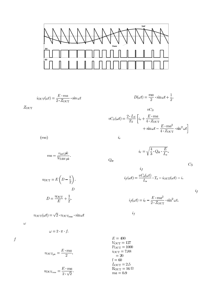
Fig. 4 shows some signals of the modulation strategy used to
drive the main switches.
The sawtooth waveform is lined on the left edge. This facili-
tates the synchronism between the auxiliary switch and the main
switches.
The converter output voltage is controlled by the amplitude
modulation factor
, which is obtained through the relation
between the peak value of the sinusoidal reference signal and
the peak value of the sawtooth waveform
(56)
The inverter output voltage for a switching period can be ex-
pressed by
(57)
From (57) we can obtain the duty cycle
, that is
(58)
The inverter output voltage for an output period is given by
(59)
where
is expressed by
(60)
—Output Frequency
The maximum output voltage is given by
(61)
The RMS output voltage is obtained from
(62)
Equation (63) shows the inverter duty cycle obtained from (58),
(59), and (62)
(63)
Combining (54), (55), and (63), we obtain the expression of the
snubber capacitor voltage,
, given by
(64)
where
is the peak reverse recovery current of the anti-parallel
diode, which can be given by [16]
(65)
represents the reverse recovery charge of the diode.
From the analysis of the current behavior in capacitor
, the
expression of current
can be obtained
(66)
Combining (64) with (66), and making some simplifications, we
obtain the expression that represents the evolution of current
(67)
To guarantee the ZVS condition in all load ranges, the minimum
value of current
obtained from (67) must be greater than the
value obtained from (48).
V. D
ESIGN
E
XAMPLE
A. Input Data
V
bus voltage;
V
RMS output voltage;
VA output power;
A
output current;
fs
kHz
switching frequency;
Hz
output frequency;
mH load inductance;
load resistance;
modulation factor.
2224
IEEE TRANSACTIONS ON CIRCUITS AND SYSTEMS—I: REGULAR PAPERS, VOL. 52, NO. 10, OCTOBER 2005
B. Calculation of the Auxiliary Inductors
The auxiliary inductors are responsible for the
limit
during the turn-off of the main diodes. The
is directly
related to the peak reverse recovery current
of the anti-par-
allel diodes. A “snappy”
produces a large amplitude tran-
sient voltage and contributes significantly to electromagnetic
interference.
In the design procedure, a
that is usually found in the
diode datasheet was chosen. This is a simple way to obtain the
diode’s fundamental parameter for the design of the inverter. In
this case, the
chosen for the example was 40 A/ s. We
know that the current ramp rate is determined by the external
circuit, thus
V
A
s
H
(68)
The auxiliary inductors are given by
H
(69)
C. Load Impedance
The load impedance is obtained from
Hz
mH
(70)
D. Diode Choice
For satisfactory performance of the inverter, it is important to
choose a slow diode. Therefore, we opted to use the body diode
of MOSFET IRFP460, which has the following characteristics:
V
maximum reverse voltage;
A
diode average current;
C
reverse recovery charge.
E. Switching Period
kHz
s
(71)
F. Reverse Recovery Current
The reverse recovery current is given by (65)
V
H
A
(72)
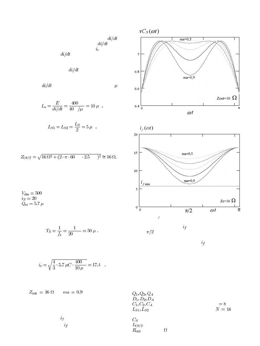
G. Capacitor Clamping Voltage Behavior
Using (64), the curves described in Fig. 5 are obtained.
For
and
, the maximum clamping
voltage is 8 V.
We can observe that the voltage increment across the switches
is smaller than in a conventional inverter.
H. Behavior of Current
The behavior of current
, obtained from (67) and (48), can
be seen in Fig. 6.
Fig. 5.
Capacitor clamping voltage behavior.
Fig. 6.
Current
i behavior.
It can be seen that current
has a minimum point that is lo-
cated at
, and the intensity of the current diminishes with the
increase of the load. To guarantee a ZVS condition in all load
ranges, the minimum value of current
, obtained from (67),
must be greater than the value of the traced straight line from (48).
VI. E
XPERIMENTAL
R
ESULTS
An inverter prototype rated 1 kVA, operating with PWM com-
mutation, was built to evaluate the proposed circuit. The main
components are given below:
A. Prototype Specifications
(IGBT IRG4PC50W);
(MOSFET body diode IRFP460);
(component’s intrinsic capacitance
nF);
(5uH each; ferrite Core EE30/7;
turns,
13 wires #20 AWG);
(220 uF/35 V; electrolytic capacitor);
(2.5 mH, output inductor);
(16
; output resistor).
MEZAROBA et al.: ZVS PWM INVERTER WITH ACTIVE VOLTAGE CLAMPING
2225
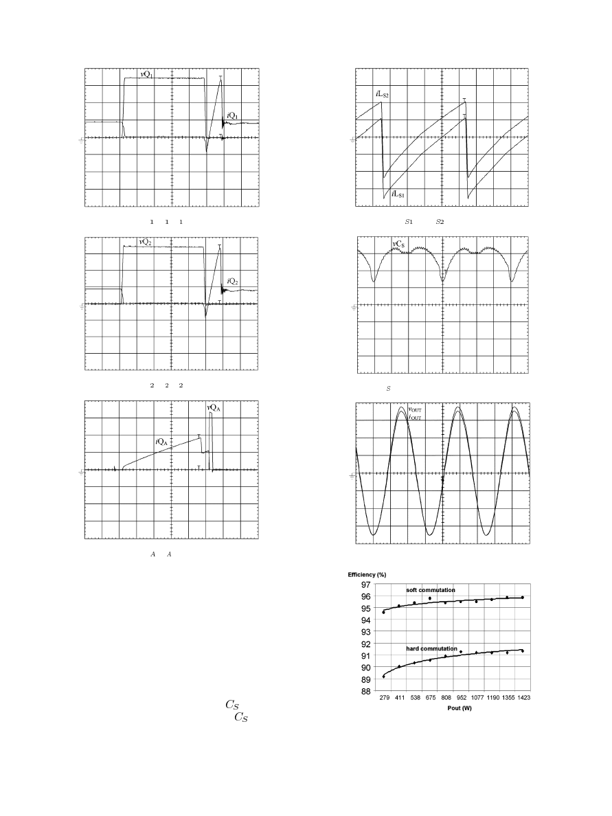
Fig. 7.
Voltage and current in
Q ; D ; C . (100 V/div, 5 A/div, 1 us/div).
Fig. 8.
Voltage and current in
Q ; D ; C . (100 V/div, 5 A/div, 1 us/div).
Fig. 9.
Voltage and current in
Q ; C . (100 V/div, 5 A/div, 1 us/div).
B. Experimental Waveforms
In the figures presented, we can observe the experimental
waveforms obtained from the laboratory prototype. Figs. 7–9
show the voltage and current in the switches. We can observe
that for all the switches, including the auxiliary one, the commu-
tation occurs under ZVS conditions, confirming the theoretical
analysis. In Fig. 10, the current in the commutation auxiliary
inductors for a switching period can be observed. A proportion-
ality of values between the currents in both inductors can be
observed. The difference between them is the load current.
The voltage across clamping capacitor
is shown in
Fig. 11. We can note a very low voltage across
, which rep-
resents a minimal voltage stress across the devices. The output
voltage and current are presented in Fig. 12. Fig. 13 shows the
efficiency as a function of the load range for both hard and soft
commutation. The converter efficiency with soft commutation
was improved by approximately 5% for all load ranges.
Fig. 10.
Current through
L
and
L . (5 A/div, 10 us/div).
Fig. 11.
Voltage in
C . (2 V/div, 2 ms/div).
Fig. 12.
Output voltage and current. (50 V/div, 5 A/div, 5 ms/div).
Fig. 13.
Efficiency versus the output power.
VII. C
ONCLUSION
A ZVS PWM inverter with voltage clamping using a single
auxiliary switch has been developed. The operation stages for a

2226
IEEE TRANSACTIONS ON CIRCUITS AND SYSTEMS—I: REGULAR PAPERS, VOL. 52, NO. 10, OCTOBER 2005
steady-state condition, mathematical analysis, main waveforms
and experimental results were presented. The experimental re-
sults show low voltage across the clamping capacitor. Switching
losses are reduced due to the implementation of a simple ac-
tive snubber circuit, which provides ZVS conditions for all the
switches, including the auxiliary one. The reduced number of
components and the simplicity of the structure increase its ef-
ficiency and reliability and make it suitable for practical appli-
cations. The proposed circuit presents soft commutation for all
load ranges, confirming the theoretical studies.
This topology presents certain advantages when compared to
the conventional soft commutation inverters studied in litera-
ture, which are:
•
soft commutation in all load ranges;
•
simple structure with a low number of components;
•
use of a classical PWM modulation;
•
auxiliary switch works with a constant duty cycle in all
operation stages;
•
use of slow and low-cost rectifier diodes;
•
low clamping voltage across the capacitor;
•
low current stress through the main switches;
•
simple design procedure with few restrictions;
•
high efficiency.
With these characteristics, the authors believe that the proposed
inverter circuit can be very useful for several industrial applica-
tions, such as: ac drive systems, power factor correction, UPS,
active filters, induction heating etc.
R
EFERENCES
[1] T. M. Undeland, “Switching stress reduction in power transistor con-
verters,” in Proc. IEEE IAS Ann. Meeting, 1976, pp. 383–391.
[2] J. Holtz, S. F. Salama, and K. Werner, “A nondissipative snubber circuit
for high-power GTO-inverters,” in Proc. IEEE IAS Ann. Meeting, 1987,
pp. 613–618.
[3] D. Tardiff and T. H. Barton, “A summary of resonant snubber circuits
for transistors and GTOs,” in Proc. IEEE IAS Ann. Meeting, 1989, pp.
1176–1180.
[4] H. G. Langer, G. Fregien;, and H. C. Skudelny, “A low loss turn-on
turn-off snubber for GTO-inverters,” in Proc. IEEE IAS Ann. Meeting,
1987, pp. 607–612.
[5] J. A. Taufiq, “Advanced inverter drivers for traction,” Proc. 5th Euro.
Conf. Power Electronics and Applications, vol. 05, pp. 224–228, Sep.
1993.
[6] A. Cheriti, “A rugged soft commutated PWM inverter for AC drivers,”
in Proc. IEEE PESC, 1990, pp. 656–662.
[7] H. Foch, M. Cheron, M. Metz, and T. Meynard, “Commutation mecha-
nisms and soft commutation in static converters,” in Proc. COBEP’91,
1991, pp. 338–346.
[8] G. Bingen, “High current and voltage transistor utilization,” in Proc.
First Eur. Conf. Power Electronics and Applications, 1985, pp.
1.15–1.20.
[9] W. Mcmurray, “Resonant snubbers with auxiliary switches,” in Proc.
IEEE IAS Ann. Meeting, 1990, pp. 829–834.
[10] R. W. De Doncker and J. P. Lyons, “The Auxiliary resonant commuted
pole converter,” in Proc. IEEE IAS Ann. Meeting, 1990, pp. 1228–1235.
[11] J. A. Bassett, “New zero voltage switching, high frequency boost con-
verter topology for power factor correction,” in Proc. INTE LEC’95,
1995, pp. 813–820.
[12] A. Pietkiewicz and D. Tollik, “New high power single-phase power
factor corrector with soft-switching,” in Proc. INTE LEC’96, 1996, pp.
114–119.
[13] D. M. Divan and G. Skibinski, “Zero-switching-loss inverters for high-
power applications,” IEEE Trans. Ind. Appl., vol. 25, no. 2, pp. 634–643,
Jul. 1989.
[14] G. Venkatamaranan and D. M. Divan, “Pulse-width resonant DC link
converter,” in Proc. IEEE IAS Ann. Meeting, 1990, pp. 984–990.
[15] H. L. Hey, C. M. O. Stein, J. R. Pinheiro, H. Pinheiro, and H. A.
Gründling, “Zero-current and zero-voltage soft-transition commutation
cell for PWM inverters,” IEEE Trans. Power Electron., vol. 19, no. 2,
2004.
[16] J. M. Peter, “Power transistor in its environment,” Thomson—CSF, Semi-
conductor Division, pp. 345–350, 1978.
Marcello Mezaroba was born in Videira, Brazil, in
1972. He received the B.S., M.S., and Ph.D. degrees
in electrical engineering from the Federal University
of Santa Catarina, Florianópolis, SC, Brazil, in 1996,
1998 and 2001, respectively.
He is presently Titular Professor in the Department
of Electrical Engineering at the State University of
Santa Catarina, Joinville, SC, Brazil.
Denizar Cruz Martins was born in Sao Paulo,
Brazil, in 1955. He received the B.S. and M.S.
degrees in electrical engineering from the Federal
University of Santa Catarina, Florianópolis, SC,
Brazil, in 1978 and 1981, respectively, and the Ph.D.
degree in electrical engineering from the Polytechnic
National Institute of Toulouse, Toulouse, France, in
1986.
He is presently Titular Professor in the Depart-
ment of Electrical Engineering at Federal University
of Santa Catarina, Brazil.
Ivo Barbi was born in Gaspar, Santa Catarina, Brazil,
in 1949. He received the B.S. and M.S. degrees in
electrical engineering from the Federal University of
Santa Catarina, Florianopolis, SC, Brazil, in 1973 and
1976, respectively, and the Dr. Ing. degree from the
Polytechnic National Institute of Toulouse, Toulouse,
France, in 1979.
He founded the Brazilian Power Electronics
Society, the Power Electronics Institute of the Fed-
eral University of Santa Catarina, and created the
Brazilian Power Electronics Conference. Currently,
he is Professor of the Power Electronics Institute, Federal University of Santa
Catarina.
Document Outline
- toc
- A ZVS PWM Inverter With Active Voltage Clamping Using the Revers
- Marcello Mezaroba, Denizar Cruz Martins, and Ivo Barbi
- Fig.€1. Proposed circuit.
- Fig.€2. Operation stages. (a) First state (t0-t1). (b) (b) Secon
- Fig.€3. Main waveforms.
- Third Stage (t2-t3): At t2, the voltage across ${C}_{1}$ reaches
- Fourth Stage (t3-t4): This stage begins when current $iL_{S1}$ i
- Fifth Stage (t4-t5): This stage starts when diode ${D}_{2}$ stop
- Sixth Stage (t5-t6): At t5, the voltage across capacitor ${C}_{A
- Seventh Stage (t6-t7): This stage begins when current $iL_{S2}$
- Eighth Stage (t7-t8): During this stage, switch ${Q}_{1}$ is blo
- Ninth Stage (t8-t0): This stage begins when the voltage across c
- IV. M ATHEMATICAL A NALYSIS OF C OMMUTATION
- Fig.€4. Modulation strategy.
- Fig.€5. Capacitor clamping voltage behavior.
- Fig.€6. Current $i_f$ behavior.
- Fig. 7. Voltage and current in ${Q}_1, {D}_1, {C}_1$ . (100 V/di
- Fig. 8. Voltage and current in ${Q}_2, {D}_2, {C}_2$ . (100 V/di
- Fig. 9. Voltage and current in ${Q}_{A}, {C}_{A}$ . (100 V/div,
- Fig. 10. Current through ${L}_{{S}1}$ and ${L}_{{S}2}$ . (5 A/di
- Fig. 11. Voltage in ${C}_{S}$ . (2 V/div, 2 ms/div).
- Fig.€12. Output voltage and current. (50 V/div, 5 A/div, 5 ms/di
- Fig.€13. Efficiency versus the output power.
- VII. C ONCLUSION
- T. M. Undeland, Switching stress reduction in power transistor c
- J. Holtz, S. F. Salama, and K. Werner, A nondissipative snubber
- D. Tardiff and T. H. Barton, A summary of resonant snubber circu
- H. G. Langer, G. Fregien;, and H. C. Skudelny, A low loss turn-o
- J. A. Taufiq, Advanced inverter drivers for traction, Proc. 5th
- A. Cheriti, A rugged soft commutated PWM inverter for AC drivers
- H. Foch, M. Cheron, M. Metz, and T. Meynard, Commutation mechani
- G. Bingen, High current and voltage transistor utilization, in P
- W. Mcmurray, Resonant snubbers with auxiliary switches, in Proc.
- R. W. De Doncker and J. P. Lyons, The Auxiliary resonant commute
- J. A. Bassett, New zero voltage switching, high frequency boost
- A. Pietkiewicz and D. Tollik, New high power single-phase power
- D. M. Divan and G. Skibinski, Zero-switching-loss inverters for
- G. Venkatamaranan and D. M. Divan, Pulse-width resonant DC link
- H. L. Hey, C. M. O. Stein, J. R. Pinheiro, H. Pinheiro, and H. A
- J. M. Peter, Power transistor in its environment, Thomson CSF, S
Wyszukiwarka
Podobne podstrony:
The Discrete Time Control of a Three Phase 4 Wire PWM Inverter with Variable DC Link Voltage and Bat
The Discrete Time Control of a Three Phase 4 Wire PWM Inverter with Variable DC Link Voltage and Bat
A new control strategy for instantaneous voltage compensator using 3 phase PWM inverter
Modified PWM Control for the DC AC Inverter With a Non Constant Voltage Source
A new control strategy for instantaneous voltage compensator using 3 phase PWM inverter
Modified PWM Control for the DC AC Inverter With a Non Constant Voltage Source
O&O Services Single Sign On on Linux using LDAP with Active Directory (2002)
00329965 Quasi Parallel Resonant Dc Link Inverter With Improved Pwm Capability
Adaptive fuzzy control for uninterruptible power supply with three phase PWM inverter
Adaptive fuzzy control for uninterruptible power supply with three phase PWM inverter
A New Medium Voltage PWM Inverter Topology for Adjustable Speed Drives
Voltage Inverter With Cascade Stage
00329965 Quasi Parallel Resonant Dc Link Inverter With Improved Pwm Capability
Inverter Negative Voltage Supply using 555 Switching Regulator
A Digital Control Technique for a single phase PWM inverter
Conducted EMI in PWM Inverter for Household Electric Appliance
dm7407 Hex Buffer Driver with High Voltage Open Collector Outputs
A Novel Switch Mode Dc To Ac Inverter With Nonlinear Robust Control
więcej podobnych podstron