Submicron sensors of local electric field with single-electron resolution
at room temperature
I. I. Barbolina and K. S. Novoselov
Department of Physics and Astronomy, University of Manchester, Manchester M13 9PL, United Kingdom
S. V. Morozov and S. V. Dubonos
Institute for Microelectronics Technology, Russian Academy of Sciences, 142432 Chernogolovka, Russia
M. Missous
Department of Electrical Engineering and Electronics, University of Manchester, Manchester M13 9PL,
United Kingdom
A. O. Volkov, D. A. Christian, I. V. Grigorieva, and A. K. Geim
a
兲
Department of Physics and Astronomy, University of Manchester, Manchester M13 9PL, United Kingdom
共Received 30 August 2005; accepted 10 November 2005; published online 3 January 2006兲
We describe probes of a local electric field, which are capable of detecting an electric charge as
small as the charge of one electron e, operational under ambient conditions and having a spatial
resolution down to 100 nm. The submicron-sized probes were made from a high-density
high-mobility two-dimensional electron gas, which is sensitive to the presence of electric charges
near its surface. We demonstrate the possibility of using such microprobes for life-science
applications by measuring an electric response of individual yeast cells to abrupt changes in their
environment. © 2006 American Institute of Physics.
关DOI:
Many areas of science and technology would benefit
from high-sensitivity local probes of electric field or charge.
A variety of such probes that provide a resolution of less than
e have recently been developed for low-temperature applica-
tions
共typically, for temperatures below 10 K兲. This includes
single-electron-transistor
共SET兲 microscopy,
1
subsurface
charge imaging,
2
the use of one-dimensional wires as voltage
probes
3–5
and the charge imaging by small field effect tran-
sistors
共FETs兲.
6
Extension of the working range of these
techniques to room temperature has remained a significant
challenge and represents a goal actively pursued by many
groups.
7–12
Indeed, sensitive local probes of an electric field
operational under ambient conditions could offer a variety of
new applications, especially for life sciences
共e.g., as an al-
ternative to patch-clamping methods
兲.
13–15
In this letter, we
describe a further development of local charge-sensitive
techniques, where the important milestone of a single-
electron resolution at room temperature has been achieved.
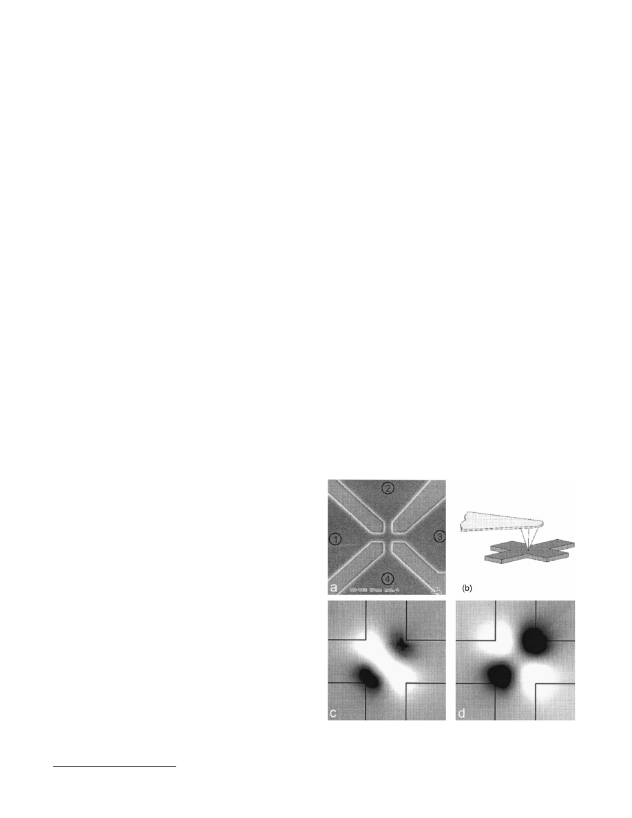
The devices used in our experiments had the Hall cross
geometry
关Fig. 1共a兲兴 and were made by electron-beam
lithography
16
from a GaAs/ InGaAs heterostructure with a
two-dimensional electron gas
共2DEG兲 embedded at a dis-
tance d
⬇70 nm below the surface. The 2DEG contained
electrons in concentration n
⬇4⫻10
16
m
−2
and with mobil-
ity of
⬇0.8 m
2
V s at 300 K. We have studied Hall crosses
with the width w between 0.3
m and 3
m. The use of a
high concentration 2DEG in conjunction with its high
mobility was found to be important for achieving the
single-electron resolution, as this ensured a low level of
intrinsic noise.
16
The basic principle of operation of the devices as charge-
sensitive detectors is as follows. If a charged object is placed
on top of such a cross above its sensitive central area, screen-
ing of the charge by nearby electrons leads to changes in a
local concentration in the 2DEG. These changes, in turn,
result in conductance changes, which can be detected by
standard lock-in techniques. Note that GaAlAs heterostruc-
tures have a highly insulating top layer, so that there is no
direct electric contact between the studied object and detec-
tor and the only interaction between the two is electrostatic.
The spatial resolution of such sensors is determined by
their size. The best resolution is achieved when all informa-
tion about changes in conductance is collected locally from
the central area w
⫻w in size 共Fig. 1兲. This can be done by
a
兲
Electronic mail: geim@man.ac.uk
FIG. 1.
共a兲 Micrograph of one of our devices with width w⬇1
m.
共b兲
Basic setup used in our studies.
共c and d兲 Spatial response to a charge placed
at an AFM tip in the bend and Hall resistance geometry, respectively. Bright
areas correspond to a decrease in resistance and dark areas to its increase for
a positive charge at the tip. Thick black lines indicate the Hall cross’ edges.
APPLIED PHYSICS LETTERS 88, 013901
共2006兲
0003-6951/2006/88
共1兲/013901/3/$23.00
© 2006 American Institute of Physics
88, 013901-1
Downloaded 13 Jul 2009 to 130.88.75.110. Redistribution subject to AIP license or copyright; see http://apl.aip.org/apl/copyright.jsp
using two measurement geometries. In one of them
共Hall
geometry
兲, an electric current is passed through the opposite
contacts of the cross
关e.g., Contacts 1 and 3 in Fig. 1共a兲兴
while voltage is measured between the other two
共2 and 4兲.
In the alternative
共bend兲 geometry, the current is flowing
between two adjacent contacts
共e.g., Contacts 1 and 2兲 and
the voltage drop is detected across the other pair
共3 and 4兲.
To determine the spatial resolution in the two geom-
etries, we scanned a charged tip of an atomic force micro-
scope
共AFM兲 above the devices 关Fig. 1共b兲兴 and simulta-
neously recorded changes in their resistance.
6
The charge on
the tip was controlled by applying
共gate兲 voltage between the
tip and 2DEG. Figures 1
共c兲 and 1共d兲 map changes in the
local resistance as a function of the tip’s position. In the bend
geometry, changes were largest when the tip was above the
diagonal separating the current contacts. The situation for the
Hall geometry was somewhat more complicated, because the
resistance changed its sign as the tip scanned over the cross
关Fig. 1共d兲兴. When averaged over the central area, the mea-
sured signal was zero, as expected from symmetry consider-
ations. Hence, the Hall geometry cannot be used for mea-
surements of electric fields created by objects larger than w.
On the other hand, if a studied object is small and placed at
one of the corners, the detected signal is of the same magni-
tude as for the bend geometry. This feature can be used to
increase the spatial resolution. To this end, we covered three
quadrants of a Hall cross by a layer of an electron-beam
resist, leaving one quadrant open. Only when a charged tip
was above the open area, a notable response was detected.
Importantly, as noise generally increases with decreasing w,
the approach allowed us to improve the spatial resolution to
⬍w/2, without decreasing a signal-to-noise ratio. Our small-
est
devices
共w⬇0.3
m
兲 allowed the resolution of
⬇100 nm.
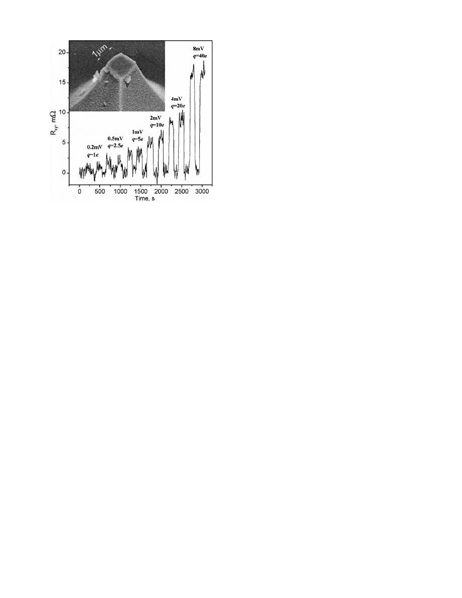
To quantify the charge sensitivity, we fabricated a spe-
cial AFM tip with a flat end of size S = 1
m
⫻1
m
共Fig.
2
兲. The flat-tip geometry provides a well-defined capacitive
coupling C with the 2DEG and therefore allows straightfor-
ward calculations of the charge q = CV at the end of the tip
for a given V. The capacitance was measured experimentally
and given by C =
0
S/共d+h兲, and ⬇13 and
0
are the
permittivity of GaAs and free space, respectively. To avoid
any mechanical damage, the tip was not in direct contact
with the probe but placed at a small distance h
⬇10 nm
above the GaAs surface. The distance was controlled by us-
ing the AFM force mode. Figure 2 shows an example of the
resistive response to different V. One can see that V as small
as 0.2 mV could be detected, which corresponds to charge
q
⬇1e located on the flat area of the AFM tip 共signal-to-noise
ratio
⬇1兲. For the integration time of 1 s in our experiments,
this yields a charge resolution of
⬇1e Hz
1/2
at low frequen-
cies. The resolution decreased by a factor of 3 for our small-
est probes
共⬇0.3
m
兲.
It is instructive to compare our devices with SET re-
nowned for their exceptional charge sensitivity. Indeed, in
several recent experiments,
7,8
SET with a size of a central
island of
⬇10 nm were shown to be operational at 300 K
and have a sensitivity better than
⬇0.1e Hz
1/2
. However, the
latter is attributed to an internal charge that is placed directly
on the central nm-sized island. It requires typically
⬇0.1 V
on an extended gate
共large C兲 in order to change a SET
resistance significantly.
7
Sensitivity to electric fields on the
level of
⬇1 mV or to external charges ⬇e has not been
demonstrated for room-temperature SET. Moreover, because
the central island is normally embedded well below the sur-
face and strongly screened by nearby source and drain con-
tacts, it will be a challenge to translate the basic sensitivity of
room-temperature SET to their sensitivity with respect to
external charges.
Finally, to demonstrate possible life-science applications,
we have used the technique to detect bioelectrical activity of
individual living cells. From the viewpoint of physics, life
can essentially be seen as motion of charges, and one can
expect that living cells generate local fields due to the motion
of ions required for biological functioning. We chose to
study yeast cells and fabricated multisensor devices shown in
Fig. 3. The size of an individual yeast cell is
⬇5
m and the
employed geometry allowed comparison between signals
from a cell placed at one of the sensors
共Fig. 3兲 with signals
from the other crosses used for abiotic control. The measure-
ments were carried out in the standard nutrient medium at
300 K
共contact regions with open metallization were spe-
cially insulated
兲. A drop of a yeast culture was placed on top
of the probe, after which a single cell was positioned at one
of the crosses using a micromanipulator.
Because water between the cell and the 2DEG probe
provided strong electric screening, we minimized this sepa-
ration by first drying the prepared samples in air. During this
procedure, cells became attached to the surface, which was
observed as their strong adhesion to particular positions on
the device. The yeast cells were not damaged by drying and
exhibited consecutive growth after immersing them in a nu-
trient medium. Despite many experiments, no signal was de-
tected from normally growing yeast cells, even with single-
electron resolution. We attribute this to their low activity at
the timescale of
⬇1 to 100 s accessible in our experiments.
Following the approach demonstrated in Ref. 14, where
electric signals from neurons were detected after stimulating
them with an electric current, we also tried stimulating yeast
cells. This was done by adding ethanol to the nutrient, which
FIG. 2. Changes in resistance induced by voltage applied to the AFM tip
shown in the inset. Here, we used the Hall geometry and the tip was placed
above one of the corners
共w⬇2
m
兲. Numbers above the peaks indicate V
and the corresponding charge q at the flat surface of the tip. For each value,
the voltage was applied twice for 2 min with a 2 min interval in between.
Inset: SEM micrograph of the flat-ended AFM tip used in these experiments.
013901-2
Barbolina et al.
Appl. Phys. Lett. 88, 013901
共2006兲
Downloaded 13 Jul 2009 to 130.88.75.110. Redistribution subject to AIP license or copyright; see http://apl.aip.org/apl/copyright.jsp
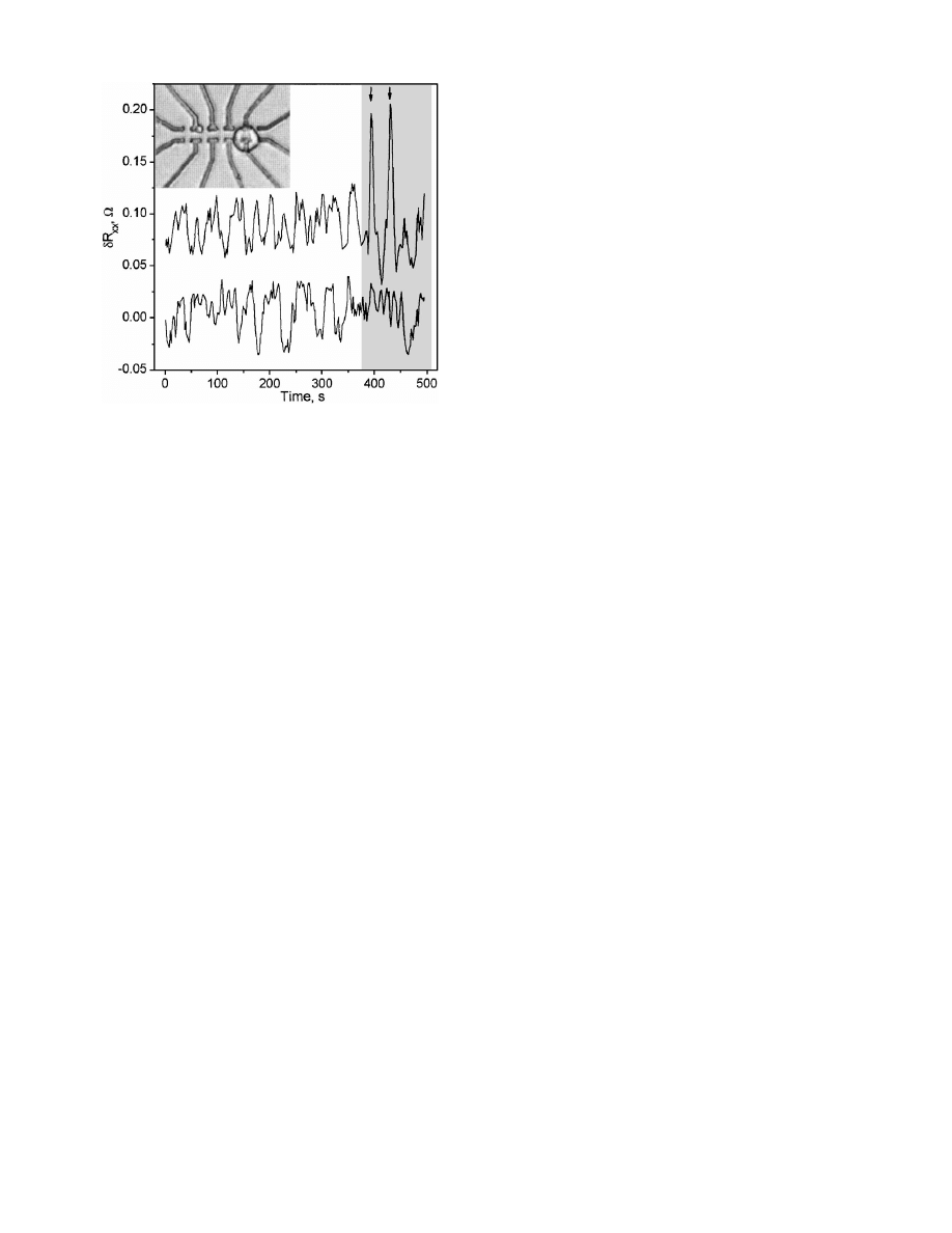
disrupted the membrane functioning. As seen in Fig. 3, yeast
cells typically reacted to the changes in chemical environ-
ment by producing several distinct peaks corresponding to
ejection of negative ions, which were detected by our sensors
well above the noise level. Assuming the ions ejected some-
where close to the sensor’s surface, the amplitude of the
observed peaks corresponds to
⬇10e. No correlated signal
was detected at any of the reference sensors. We attribute the
observed signals to a transient imbalance in ion concentra-
tions around the cell as a result of the distraction of its
membrane’s functioning.
With reference to life-science applications, the presented
approach should be compared with the existing FET
techniques.
13–15
In the latter case, relatively large Si-FET de-
vices with an active area of
⬇100
m
2
were used which
allowed one to avoid excess noise characteristic to mesos-
copic devices and maintain sensitivity to changes in gate
voltage
␦
V on the level
⬇0.1 to 1 mV. The above dimen-
sions result in C
⬇0.1 to 1 pF, which corresponds to the
charge resolution of
⬇10
2
to 10
4
electrons. On the contrary,
our devices are optimized for the local charge detection.
While capable of detecting
␦
V on the same level of 0.1 mV,
our approach provides two orders better sensitivity with re-
spect to an external charge and, at the same time, collects
information from submicron area.
In conclusion, our work demonstrates the possibility of
detection of external charges at the level of one electron at
room temperature and in biological solutions. Submicron
sensors made from a high-mobility high-concentration
2DEG can also be used for scanning probe microscopy,
providing a deep-submicron resolution for imaging of local
electric fields and charges. The detected response from
individual yeast cells indicates the technique’s potential for
life-science applications.
This work was supported by EPSRC and MRC
共UK兲.
1
M. J. Yoo T. A. Fulton, H. F. Hess, R. L. Willett, L. N. Dunkleberger,
R. J. Chichester, L. N. Pfeiffer, and K. W. West, Science 276, 579
共1997兲.
2
S. H. Tessmer, P. I. Glicofridis, R. C. Ashoori, L. S. Levitov, and M. R.
Melloch, Nature
共London兲 392, 51 共1998兲.
3
R. Taboryski, K. Baklanov, and P. E. Lindelof, Phys. Rev. Lett. 70, 2475
共1993兲.
4
M. Field C. G. Smith, M. Pepper, D. A. Ritchie, J. E. F. Frost, G. A. C.
Jones, and D. G. Hasko, Phys. Rev. Lett. 70, 1311
共1993兲.
5
A. T. Sellwood, C. G. Smith, E. H. Linfield, M. Y. Simmons, and D. A.
Ritchie, Rev. Sci. Instrum. 72, 2100
共2001兲.
6
L. H. Chen, M. A. Topinka, B. J. LeRoy, R. M. Westervelt, K. D.
Maranowski, and A. C. Gossard, Appl. Phys. Lett. 79, 1202
共2001兲.
7
Y. A. Pashkin, Y. Nakamura, and J. S. Tsai, Appl. Phys. Lett. 76, 2256
共2000兲.
8
T. W. Kim, D. C. Choo, J. H. Shim, and S. O. Kang, Appl. Phys. Lett. 80,
2168
共2002兲.
9
Y. Martin, D. W. Abraham, and H. K. Wickramasinghe, Appl. Phys. Lett.
52, 1103
共1988兲.
10
C. C. Williams, J. Slinkman, W. P. Hough, and H. K. Wickramasinghe,
Appl. Phys. Lett. 55, 1662
共1989兲.
11
M. Nonnenmacher, M. P. Oboyle, and H. K. Wickramasinghe, Appl. Phys.
Lett. 58, 2921
共1991兲.
12
L. J. Klein and C. C. Williams, Appl. Phys. Lett. 79, 1828
共2001兲.
13
A. Offenhausser and W. Knoll, Trends Biotechnol. 19, 62
共2001兲.
14
P. Fromherz, A. Offenhausser, T. Vetter, and J. Weis, Science 252, 1290
共1991兲.
15
J. Fritz, E. B. Cooper, S. Gaudet, P. K. Sorger, and S. K. Manalis, Proc.
Natl. Acad. Sci. U.S.A. 99, 14142
共2002兲.
16
K. S. Novoselov S. V. Morozov, S. V. Dubonos, M. Missous, A. O.
Volkov, D. A. Christian, and A. K. Geim, J. Appl. Phys. 93, 10053
共2003兲.
FIG. 3. Inset: Optical-microscope photo of a multisensor device with a live
yeast cell attached to the sensor on the right. The scale is given by a distance
of 5
m between adjacent crosses. The main panel shows time-dependent
behavior of the bend resistance for one of the reference crosses
共lower
curve
兲 and for the cross with the yeast cell on top 共upper curve兲, measured
simultaneously. A constant background
⬇980 ⍀ is subtracted from both
curves. The noise level was
⬇50 m⍀. No electric signal could be found
above noise under normal growth conditions. The shaded area indicates the
time when ethanol was added. Two peaks marked by arrows are seen for the
cross with the yeast cell attached.
013901-3
Barbolina et al.
Appl. Phys. Lett. 88, 013901
共2006兲
Downloaded 13 Jul 2009 to 130.88.75.110. Redistribution subject to AIP license or copyright; see http://apl.aip.org/apl/copyright.jsp
Wyszukiwarka
Podobne podstrony:
29 Appl Phys Lett 91 063124 200 Nieznany (2)
25 Appl Rev Lett 91 233108 2007 Nieznany (2)
56 J Appl Phys 93 10053 10057 2 Nieznany (2)
918 tech inf ark prak5 czer 200 Nieznany (2)
08 04 25 12 33 18 dispenser 200 Nieznany (2)
2 14 cw ceramika unlockedid 200 Nieznany (2)
biologia konkurs wojewodzki 200 Nieznany
Analiza wyp przy pracy PIP 200 Nieznany (3)
8 Bezpieczenstwo 87 88 by daro Nieznany (2)
hermeneutyka skroty kolo id 200 Nieznany
88 4 id 47730 Nieznany
49 J Low Temp Phys 139 65 72 20 Nieznany
Budowa mostow w Polsce 1995 200 Nieznany
11 Phys Rev B 78 085432 2008id Nieznany (2)
więcej podobnych podstron