
Raman fingerprint of charged impurities in graphene
C. Casiraghi
and S. Pisana
Engineering Department, Cambridge University, Cambridge CB3 OFA United Kingdom
K. S. Novoselov and A. K. Geim
Department of Physics and Astronomy, Manchester University, Manchester M13 9PL, United Kingdom
A. C. Ferrari
Engineering Department, Cambridge University, Cambridge CB3 OFA, United Kingdom
共Received 19 September 2007; accepted 7 November 2007; published online 5 December 2007兲
We report strong variations in the Raman spectra for different single-layer graphene samples
obtained by micromechanical cleavage. This reveals the presence of excess charges, even in the
absence of intentional doping. Doping concentrations up to
⬃10
13
cm
−2
are estimated from the G
peak shift and width and the variation of both position and relative intensity of the second order 2D
peak. Asymmetric G peaks indicate charge inhomogeneity on a scale of less than 1
m. © 2007
American Institute of Physics.
关DOI:
Graphene is the prototype two-dimensional carbon
system
and a promising candidate for future electronics.
Graphene samples are usually obtained from micromechani-
cal cleavage of graphite
and they can be identified by elastic
and inelastic light scattering, such as Rayleigh and Raman
spectroscopies.
Raman spectroscopy is a fast and nondestructive method
for the characterization of carbons.
Their Raman spectra
show common features in the 800– 2000 cm
−1
region: the G
and D peaks, which lie at around 1560 and 1360 cm
−1
, re-
spectively. The G peak corresponds to the E
2g
phonon at the
Brillouin zone center. The D peak is due to the breathing
modes of sp
2
atoms and requires a defect for its
It is common for as-prepared graphene not to
have enough structural defects for the D peak to be Raman
active,
so that it can only be seen at the edges.
However,
the most prominent feature in graphene is the second order
of the D peak: the 2D peak.
This lies at
⬃2700 cm
−1
and it
is always seen, even when no D peak is present, since no
defects are required for the activation of second order
phonons. Its shape distinguishes single and multilayer
samples. Graphene has a sharp, single 2D peak, in contrast
with graphite and few-layers graphene.
The ability to controllably dope n or p is key for appli-
cations. Raman spectroscopy can monitor doping in
graphene.
The effect of back gating and top gating on the
G-peak position
关Pos共G兲兴 and its full width at half maximum
关FWHM共G兲兴 was reported in Refs.
. Pos
共G兲 increases
and FWHM
共G兲 decreases for both electron and hole dopings.
The stiffening of the G peak is due to the nonadiabatic re-
moval of the Kohn anomaly at
⌫.
The FWHM sharpen-
ing is due to blockage of the phonon decay into electron-hole
pairs due to the Pauli exclusion principle, when the electron-
hole gap becomes higher than the phonon energy.
FWHM
共G兲 sharpening saturates when doping causes a Fermi
level shift bigger than half the phonon energy.
A similar
behavior is observed for the LO-G
−
peak in metallic
nanotubes
for the same reasons.
Most of the previous research focused on the properties
of well defined graphene layers and devices
with little effort on a systematic investigation of sample vari-
ability. Here, we show that Raman spectroscopy can finger-
print differences between nominally identical samples pro-
duced in the same way. We find that, even in the absence of
a D peak, changes in the Raman parameters are most com-
mon and relate to the presence of excess charges. This is a
significant finding, which reconciles the variation of electri-
cal properties often found for nominally identical samples.
We
study
more
than
40
as-prepared
monolayer
graphenes, produced by microcleavage of graphite. These
have different areas, from few
m
2
to 450
m
2
. Some of
them are also measured in a device configuration after depo-
sition of Au electrodes
共with a thin Cr underlayer兲. More
than
⬃100 spectra are measured using a 100⫻ objective at
514 and 633 nm, with a Renishaw spectrometer, of
⬃2 cm
−1
spectral resolution and power well below 2 mW.
Figure
plots the 514 nm spectra of different samples
normalized to the G peak. The G peak significantly shifts.
The 2D peak also shows a small change in position. The
relative intensity of the 2D and G peaks strongly varies. Fig-
ure
plots spectra measured on the same graphene
sample. This is a contacted sample, and the spectra change
moving closer to the electrodes. Figure
indicates that the
G peak can be sometimes asymmetric. Note that Fig.
does
not mean that the Raman spectra always vary in different
samples or that they always change within a given sample.
However, it warns that uniformity has to be checked, and
cannot be simply assumed. Moreover, Fig.
dismisses the
suggestion of Refs.
and
that either G peak position or
I
共2D兲/I共G兲 can be used to estimate the number of layers,
since the variation of these parameters in as deposited single
layers far exceeds that assigned to the increase of number of
layers.
Note that the criterium based on the shape of the
2D peak
still stands and allows layer counting.
Figure
plots Pos
共G兲 and FWHM共G兲. There is a clear
correlation: a Pos
共G兲 increase corresponds to a FWHM共G兲
decrease. This is quite similar to what we observed in inten-
tionally doped graphene, where the Fermi energy was modu-
lated using a gate.
Indeed, the continuous line in Fig.
plots the theoretical correlation between Pos
共G兲 and
FWHM
共G兲 obtained from combining Eqs. 共6兲 and 共7兲 of
a
兲
Current Address: Physics dep., Freie Universität, Arnimallee 14, D-14195
Berlin, Germany.
b
兲
Electronic mail: acf26@eng.cam.ac.uk.
APPLIED PHYSICS LETTERS 91, 233108
共2007兲
0003-6951/2007/91
共23兲/233108/3/$23.00
© 2007 American Institute of Physics
91, 233108-1
Downloaded 13 Jul 2009 to 130.88.75.110. Redistribution subject to AIP license or copyright; see http://apl.aip.org/apl/copyright.jsp
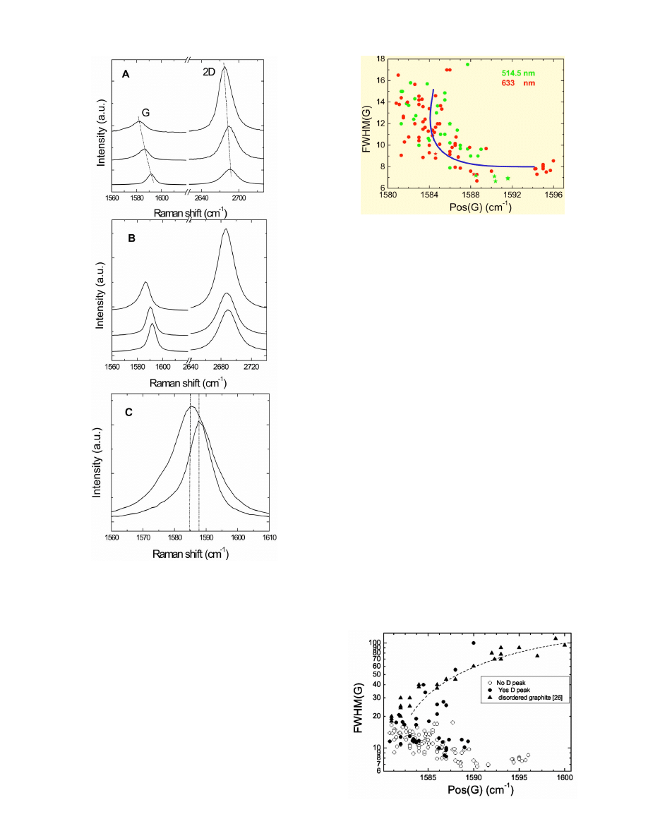
Ref.
. The agreement with experiments is remarkable con-
sidering that Ref.
studied a single sample as a function of
doping, while Fig.
is a collection of measurements on tens
of different samples with no intentional control of doping.
The star data points in Fig.
are measurements on contacted
samples. Interestingly, they usually have significant doping.
This is consistent with chemical doping during microfabrica-
tion procedures, which can often be seen as a shift of the
charge
neutrality
point
away
from
zero
gate
voltage.
However, it is quite remarkable that
“pristine” samples, with no contacts, exhibit almost an order
of magnitude doping variation, with a few showing a very
high doping over
⬃10
13
cm
−2
. Excess charges can be due to
substrate, adsorbates, and resist/process residuals.
In con-
tacted samples, the difference of work function between
sample and contacts can also contribute to the doping varia-
tion across the layer.
Figure
shows that the maximum FWHM
共G兲 for the
most intrinsic samples is
⬃16 cm
−1
, slightly higher than in
graphite.
Note that all spectra used to derive Fig.
do not
show any D peak. Thus, we exclude a significant influence of
defects in the measured trend. Interestingly, as already ob-
served in Refs.
and
, FWHM
共G兲 never becomes
smaller than
⬃6 cm
−1
, while for very high doping we would
expect the minimum FWHM
共G兲 to be close to our spectral
resolution
共⬃2 cm
−1
兲. This implies an inhomogeneous distri-
bution of charges within the laser spot of
⬃1
m
2
even for
high self-doping, or a non-adiabatic increase of anharmonic-
ity for high doping. The asymmetric spectra of Fig.
in-
dicate even larger variations.
Figure
includes data from samples with a D peak.
Some fall in the same FWHM
共G兲/Pos共G兲 relation for
D-peak-free samples, indicating that they originate from
sample edges, not from disorder. However, others have
FWHM
共G兲 above 16 cm
−1
, the maximum measured for
D-peak-free samples, accompanied by a stiffening of the G
peak. This is a signature of structural disorder.
Indeed,
in the case of graphite, it is known that, for increasing de-
fects leading to nanocrystalline graphite, FWHM
共G兲 and
Pos
共G兲 both increase,
the opposite of what happens for
increasing doping. Thus, a large FWHM
共G兲, together with
Pos
共G兲 close to 1580 cm
−1
and no D peak, fingerprint the
most intrinsic samples, while a large FWHM
共G兲, Pos共G兲
FIG. 1.
共a兲 514 nm spectra of three different graphene samples. 共b兲 Spectra
in three different points of the same sample.
共c兲 The G peak can sometimes
be asymmetric.
FIG. 2.
共Color online兲 FWHM共G兲 and Pos共G兲 at 514 and 633 nm. Stars
indicate samples with metallic contacts. Only spectra without D peak are
fitted. The solid line is the theory for doped graphene at 300 K
共Ref.
兲,
giving more than 10
13
cm
−2
doping for the bottom-right samples
共Refs.
and
兲.
FIG. 3. FWHM
共G兲 and Pos共G兲 for graphene with and without D peak and
for nanocrystalline graphite
共Ref.
兲.
233108-2
Casiraghi et al.
Appl. Phys. Lett. 91, 233108
共2007兲
Downloaded 13 Jul 2009 to 130.88.75.110. Redistribution subject to AIP license or copyright; see http://apl.aip.org/apl/copyright.jsp
higher than 1580 cm
−1
and a D peak indicate structural
disorder.
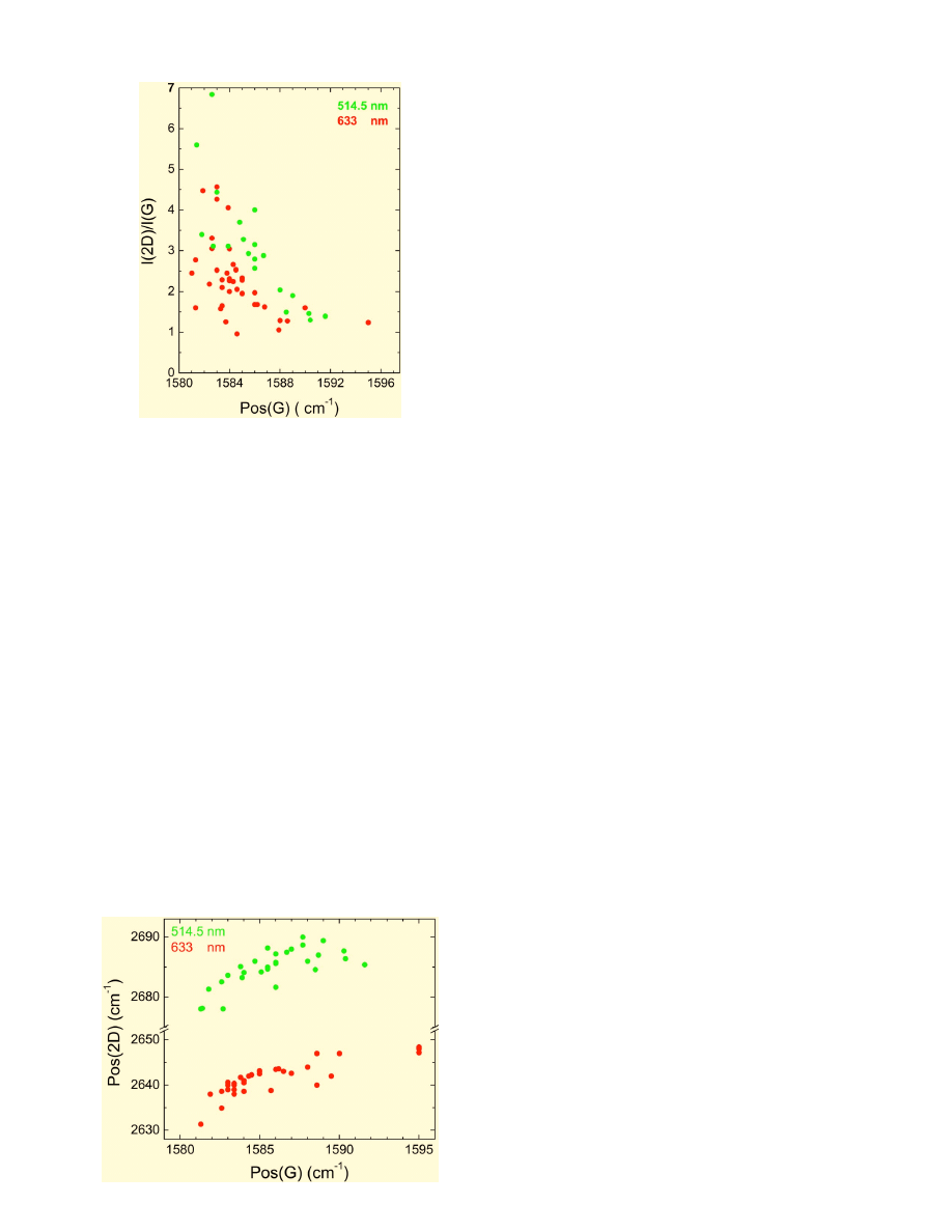
We now analyze the 2D peak. Figure
plots I
共2D兲/I共G兲
as a function of Pos
共G兲. This clearly shows a large variation
with doping: at low doping the 2D peak is 3–5 times stronger
than the G peak, depending on the excitation wavelength; at
high doping
共for a G peak position above 1592 cm
−1
兲 the
intensity ratio is
⬃1.
Figure
correlates Pos
共2D兲 and Pos共G兲. Unlike the G
peak, the 2D peak always upshifts with excitation energy due
to double resonance.
The dispersion with excitation en-
ergy is 95– 85 cm
−1
/eV. Figure
also shows that the 2D
peak is sensitive to doping. Doping has two major effects:
共i兲
modification of the equilibrium lattice parameter with a con-
sequent stiffening/softening of the phonons;
and
共ii兲 onset
of dynamic effects beyond the Born-Oppenheimer approxi-
mation that modify the phonon dispersions close to the Kohn
anomalies.
For the 2D peak, the influence of dynamic
effects is expected to be negligible, since the 2D phonons are
far away from the Kohn anomaly at K.
Thus, the varia-
tion of the 2D peak with doping is mainly due to charge
transfer, with hole doping resulting in an upshift, and the
opposite for high electron doping.
Indeed, FWHM
共2D兲
does not show the same trend as FWHM
共G兲, but is
⬃28–30 cm
−1
for all samples. Since Fig.
indicates 2D
stiffening with increasing Pos
共G兲, we conclude that most of
our samples show hole doping. This agrees with what found
in electrical measurements, where the charge neutrality
points are mostly reached for positive gate bias.
Adsor-
bants induce chemical doping and water could explain the p
doping.
In conclusion, we presented a systematic analysis of the
Raman spectra of as-deposited graphene. When no D peak is
present, the large variation in Raman parameters is assigned
to charged impurities. Variations in the Raman spectra can
also be observed within the same sample, indicating in-
homogeneous charges. A D peak far from the edge means
structural disorder. Thus, Raman is a powerful tool to moni-
tor the “quality” of graphene.
C.C. acknowledges the Oppenheimer Fund. ACF, AKG,
KSN the Royal Society, and Leverhulme Trust.
1
A. K. Geim and K. S. Novoselov, Nat. Mater. 6, 183
共2007兲.
2
M. Y. Han, B. Ozyilmaz, Y. Zhang, and P. Kim, Phys. Rev. Lett. 98,
206805
共2007兲.
3
M. C. Lemme, T. J. Echtermeyer, M. Baus, and H. Kurz, IEEE Electron
Device Lett. 28, 282
共2007兲.
4
Z. Chen, Y. M. Lin, M. J. Rooks, and P. Avouris, e-print arXiv:cond-mat/
0701599.
5
K. S. Novoselov, D. Jiang, F. Schedin, T. J. Booth, V. V. Khotkevich, and
S. V. Morozov, Proc. Natl. Acad. Sci. U.S.A. 102, 10451
共2005兲.
6
C. Casiraghi, A. Hartschuh, E. Lidorikis, H. Qian, H. Harutyunyan, T.
Gokus, K. S. Novoselov, and A. C. Ferrari, Nano Lett. 7, 2177
共2007兲.
7
A. C. Ferrari, J. C. Meyer, V. Scardaci, C. Casiraghi, M. Lazzeri, F. Mauri,
S. Piscanec, D. Jiang, K. S. Novoselov, S. Roth, and A. K. Geim, Phys.
Rev. Lett. 97, 187401
共2006兲.
8
Raman Spectroscopy in Carbons: From Nanotubes to Diamond, edited by
A. C. Ferrari and J. Robertson, special issue in Philos. Trans. R. Soc.
London, Ser. A 362, 2267
共2004兲.
9
F. Tuinstra and J. L. Koenig, J. Chem. Phys. 53, 1126
共1970兲.
10
A. C. Ferrari and J. Robertson, Phys. Rev. B 61, 14095
共2000兲; 64,
075414
共2001兲.
11
C. Thomsen and S. Reich, Phys. Rev. Lett. 85, 5214
共2000兲.
12
S. Pisana, M. Lazzeri, C. Casiraghi, K. Novoselov, A. K. Geim, A. C.
Ferrari, and F. Mauri, Nat. Mater. 6, 198
共2007兲.
13
A. Das, S. Pisana, S. Piscanec, B. Chakraborty, S. K. Saha, U. V.
Waghmare, R. Yang, H. R. Krishnamurhthy, A. K. Geim, A. C. Ferrari,
and A. K. Sood, arXiv:cond-mat/0709.1174v1.
14
J. Yan, Y. B. Zhang, P. Kim, and A. Pinczuk, Phys. Rev. Lett. 98, 166802
共2007兲.
15
M. Lazzeri and F. Mauri, Phys. Rev. Lett. 97, 266407
共2006兲.
16
M. Lazzeri, S. Piscanec, F. Mauri, A. C. Ferrari, and J. Robertson, Phys.
Rev. B 73, 155426
共2006兲.
17
Y. Wu, J. Maultzsch, E. Knoesel, B. Chandra, M. Huang, M. Y. Sfeir, L. E.
Brus, J. Hone, and T. F. Heinz, Phys. Rev. Lett. 99, 027402
共2007兲.
18
K. T. Nguyen, A. Gaur, and M. Shim, Phys. Rev. Lett. 98, 145504
共2007兲.
19
K. S. Novoselov, A. K. Geim, S. V. Morozov, D. Jiang, Y. Zhang, S. V.
Dubonos, I. V. Grigorieva, and A. A. Firsov, Science 306, 666
共2004兲.
20
Y. Y. Zhang, Y. W. Tan, H. L. Stormer, and P. Kim, Nature
共London兲 438,
201
共2005兲.
21
A. Gupta, G. Chen, P. Joshi, S. Tadigadapa, and P. C. Eklund, Nano Lett.
6, 2667
共2006兲.
22
D. Graf, F. Molitor, K. Ensslin, C. Stampfer, A. Jungen, C. Hierold, and L.
Wirtz, Nano Lett. 7, 238
共2007兲.
23
Y. W. Tan, Y. Zhang, K. Bolotin, Y. Zhao, S. Adam, E. H. Hwang, D. Das
Sarma, H. L. Sormer, and P. Kim, arXiv:cond-mat/0707.1870.
24
J. Martin, N. Akerman, G. Ulbricht, T. Lohmann, J. H. Smet, K.
von Klitzing, and A. Yacoby, arXiv:cond-mat/0705.2180.
25
S. Piscanec, M. Lazzeri, F. Mauri, A. C. Ferrari, and J. Robertson, Phys.
Rev. Lett. 93, 185503
共2004兲.
26
P. Lespade, A. Marchard, M. Couzi, and F. Cruege, Carbon 22, 375
共1984兲.
27
A. C. Ferrari, Solid State Commun. 143, 47
共2007兲.
28
L. Pietronero and S. Strassler, Phys. Rev. Lett. 47, 593
共1981兲.
29
F. Schedin, A. K. Geim, S. V. Morozov, E. W. Hill, P. Blake, M. I.
Katsnelson, and K. S. Novoselov, Nat. Mater. 6, 652
共2007兲.
FIG. 4.
共Color online兲 I共2D兲/I共G兲 as a function of Pos共G兲.
FIG. 5.
共Color online兲 Pos共2D兲 as a function Pos共G兲 at 514 and 633 nm.
233108-3
Casiraghi et al.
Appl. Phys. Lett. 91, 233108
共2007兲
Downloaded 13 Jul 2009 to 130.88.75.110. Redistribution subject to AIP license or copyright; see http://apl.aip.org/apl/copyright.jsp
Wyszukiwarka
Podobne podstrony:
29 Appl Phys Lett 91 063124 200 Nieznany (2)
43 Appl Phys Lett 88 013901 200 Nieznany (2)
43 Appl Phys Lett 88 013901 200 Nieznany (2)
24 Phys Rev Lett 99 216802 2007
32 Phys Rev Lett 98 196806 2007
III CZP 15 91 id 210268 Nieznany
Mapy polityczne konturowe 2007 Nieznany
30 Nature Mater 6 652 655 2007 Nieznany (2)
Mapy polityczne konturowe 2007 Nieznany (2)
I ACR 184 91 id 208160 Nieznany
passat 91 id 350144 Nieznany
AGPA Practice Guidelines 2007 P Nieznany (2)
12 Nano Lett 8 2442 2446 2008id Nieznany (2)
37 Phys Rev Lett 97 187401 2006
51 Phys Rev Lett 92 237001 2004
41 Phys Rev Lett 97 016801 2006
więcej podobnych podstron