
Biased Bilayer Graphene: Semiconductor with a Gap Tunable by the Electric Field Effect
Eduardo V. Castro,
1
K. S. Novoselov,
2
S. V. Morozov,
2
N. M. R. Peres,
3
J. M. B. Lopes dos Santos,
1
Johan Nilsson,
4
F. Guinea,
5
A. K. Geim,
2
and A. H. Castro Neto
4,6
1
CFP and Departamento de Fı´sica, Faculdade de Cieˆncias Universidade do Porto, P-4169-007 Porto, Portugal
2
Department of Physics and Astronomy, University of Manchester, Manchester, M13 9PL, United Kingdom
3
Center of Physics and Departamento de Fı´sica, Universidade do Minho, P-4710-057 Braga, Portugal
4
Department of Physics, Boston University, 590 Commonwealth Avenue, Boston, Massachusetts 02215, USA
5
Instituto de Ciencia de Materiales de Madrid, CSIC, Cantoblanco, E-28049 Madrid, Spain
6
Department of Physics, Harvard University, Cambridge, Massachusetts 02138, USA
(Received 15 November 2006; published 20 November 2007)
We demonstrate that the electronic gap of a graphene bilayer can be controlled externally by applying a
gate bias. From the magnetotransport data (Shubnikov– de Haas measurements of the cyclotron mass),
and using a tight-binding model, we extract the value of the gap as a function of the electronic density. We
show that the gap can be changed from zero to midinfrared energies by using fields of & 1 V=nm, below
the electric breakdown of SiO
2
. The opening of a gap is clearly seen in the quantum Hall regime.
DOI:
PACS numbers: 73.20.At, 73.21.Ac, 81.05.Uw
The electronic structure of materials is given by their
chemical composition and specific arrangements of atoms
in a crystal lattice and, accordingly, can be changed only
slightly by external factors such as temperature or high
pressure. In this Letter we show, both experimentally and
theoretically, that the band structure of bilayer graphene
can be controlled by an applied electric field so that the
electronic gap between the valence and conduction bands
can be tuned between zero and midinfrared energies. This
makes bilayer graphene the only known semiconductor
with a tunable energy gap and may open the way for
developing photodetectors and lasers tunable by the elec-
tric field effect. The development of a graphene-based
tunable semiconductor being reported here, as well as the
discovery of anomalous integer quantum Hall effects
(QHE) in single-layer [
,
] and unbiased bilayer [
] gra-
phene, which are associated with massless [
] and massive
] Dirac fermions, respectively, demonstrate the potential
of these systems for carbon-based electronics [
].
Furthermore, the deep connection between the electronic
properties of graphene and certain theories in particle
physics makes graphene a test bed for many ideas in basic
science.
Below we report the experimental realization of a
tunable-gap graphene bilayer and provide its theoretical
description in terms of a tight-binding model corrected by
charging effects (Hartree approach) [
]. Our main findings
are as follows: (i) in a magnetic field, a pronounced plateau
at zero Hall conductivity
xy
0 is found for the biased
bilayer, which is absent in the unbiased case and can only
be understood as due to the opening of a sizable gap,
g
,
between the valence and conductance bands; (ii) the cy-
clotron mass, m
c
, in the bilayer biased by chemical doping
is an asymmetric function of carrier density, n, which
provides a clear signature of a gap and allows its estimate;
(iii) by comparing the observed behavior with our tight-
binding results, we show that the gap can be tuned to values
larger than 0.2 eV; (iv) we have cross-checked our theory
against
angle-resolved
photoemission
spectroscopy
(ARPES) data [
] and found excellent agreement.
The devices used in our experiments were made from
bilayer graphene prepared by micromechanical cleavage of
graphite on top of an oxidized silicon wafer (300 nm of
SiO
2
) [
]. By using electron-beam lithography, the gra-
phene samples were then processed into Hall bar devices
similar to those reported in Refs. [
]. To induce charge
carriers, we applied a gate voltage V
g
between the sample
and the Si wafer, which resulted in carrier concentrations
n
1
V
g
due to the electric field effect. The coefficient
7:2 10
10
cm
2
=V is determined by the geometry of
the resulting capacitor and is in agreement with the values
of n
1
found experimentally [
]. In order to control
independently the gap value and the Fermi level E
F
, the
devices could also be doped chemically by exposing them
to NH
3
that adsorbed on graphene and effectively acted as
a top gate providing a fixed electron density n
0
[
]. The
total bilayer density n is then n n
1
n
0
relatively to half
filling. The electrical measurements were carried out by
the standard lock-in technique in magnetic fields up to 12 T
and at temperatures between 4 and 300 K.
We start by showing experimental evidence for the gap
opening in bilayer graphene. Figure
shows the mea-
sured Hall conductivity of bilayer graphene, which allows
a comparison of the QHE behavior in the biased and
unbiased cases. Here the curve labeled ‘‘pristine’’ shows
the anomalous QHE that is characteristic of the unbiased
bilayer [
]. In this case, the Hall conductivity exhibits a
sequence of plateaus at
xy
4Ne
2
=h
where N is integer
and the factor 4 takes into account graphene’s quadruple
degeneracy. The N 0 plateau is strikingly absent, so that
a double step of 8e
2
=h
in height occurs at n 0, indicating
a metallic state at the neutrality point [
]. Note that the
backgate voltage induces asymmetry between the two
layers but QHE measurements can only probe states close
PRL 99, 216802 (2007)
P H Y S I C A L
R E V I E W
L E T T E R S
week ending
23 NOVEMBER 2007
0031-9007= 07=99(21)=216802(4)
216802-1
© 2007 The American Physical Society
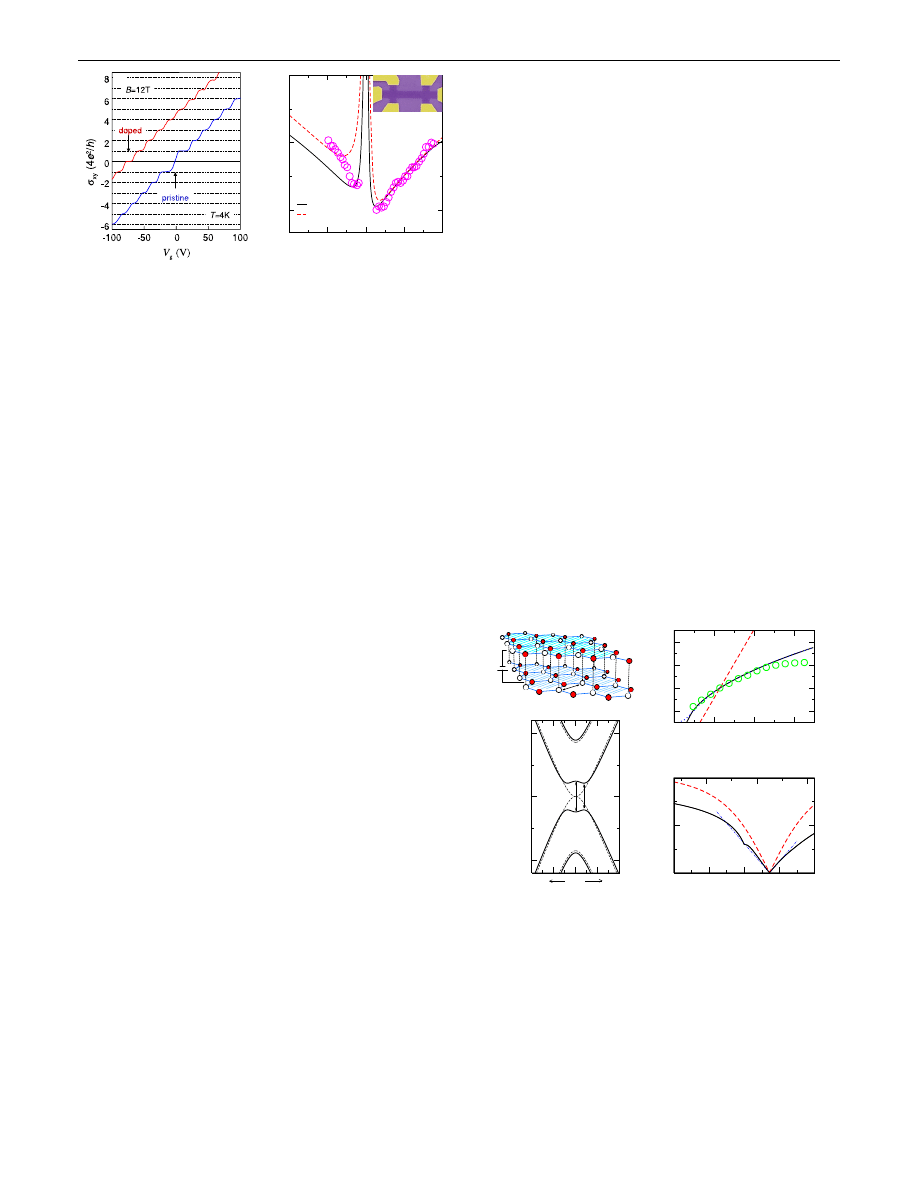
to E
F
and are not sensitive to the presence (or absence) of a
gap below the Fermi sea. To probe the gap that is expected
to open at finite V
g
, we first biased the bilayer devices
chemically and then swept V
g
through the neutrality point,
in which case E
F
passes between the valence and conduc-
tion bands at high V
g
. The energy gap is revealed by the
appearance of the N 0 plateau at
xy
0 [see the curve
labeled ‘‘doped’’ in Fig.
]. The emerged plateau was
accompanied by a huge peak in longitudinal resistivity
xx
,
indicating an insulating state (in the biased device,
xx
at
n 0 exceeded 150 kOhm at 4 K, as compared to
6 kOhm for the unbiased case under the same conditions).
The recovered sequence of equidistant plateaus represents
the ‘‘standard’’ integer QHE that would be expected for an
ambipolar semiconductor with an energy gap exceeding
the cyclotron energy. The latter is estimated to be
>40 meV in the case of Fig.
To gain further information about the observed gap, we
measured the cyclotron mass of charge carriers and its
dependence on n. To this end, we followed the same
time-consuming procedure as described in detail in
Ref. [
] for the case of single-layer graphene. In brief,
for many different gate voltages, we measured the tem-
perature (T) dependence of Shubnikov –de Haas oscilla-
tions and then fitted their amplitude by the standard
expression T= sinh2
2
k
B
Tm
c
=
@eB. To access electronic
properties of both electrons and holes in the same chemi-
cally biased device, we chose to dope it to n
0
1:8
10
12
cm
2
, i.e., less than in the case of Fig.
. The
results are shown in Fig.
. The linear increase of m
c
with jnj and the pronounced asymmetry between hole- and
electron-doping of the biased bilayer are clearly seen here.
To explain the observed Hall conductivity and cyclotron
mass data for bilayer graphene, in what follows, we shall
use a tight-binding description of electrons in bilayer gra-
phene. Its carbon atoms are arranged in two honeycomb
lattices labeled 1 and 2 and stacked according to the Bernal
order (A1 –B2), where A and B refer to each sublattice
within each honeycomb layer, as shown in Fig.
. The
system is parametrized by a tight-binding model where
electrons are allowed to hop between nearest-neighbor
sites, with in-plane hopping t and interplane hopping t
?
.
Throughout the Letter we use t 3:1 eV and t
?
0:22 eV. The value of t is inferred from the Fermi-Dirac
velocity
in
graphene,
v
F
2
p
=3at=
@ 10
6
ms
1
,
where a 2:46
A is the same-sublattice carbon-carbon
distance, and t
?
is extracted by fitting m
c
(see below).
For the biased system the two layers gain different electro-
static potentials, and the corresponding energy difference
is given by eV. The presence of a perpendicular magnetic
field B B^e
z
is accounted for through the standard Peierls
substitution, t ! texpfie
R
R
R
A
drg, where e is the elec-
tron charge, the vector connecting nearest-neighbor sites,
and A the vector potential (in units such that c 1
@).
Figure
shows the electronic structure of the biased
bilayer near the Dirac points (K or K
0
). In agreement with
the Hall conductivity results in Fig.
, one can see that
the unbiased gapless semiconductor (dashed line) be-
comes, with the application of an electrostatic potential
V
, a small-gap semiconductor (solid line) whose gap is
given by:
g
e
2
V
2
t
2
?
=t
2
?
e
2
V
2
1=2
. As V can be
externally controlled, this model predicts that biased bi-
layer graphene should be a tunable-gap semiconductor, in
agreement with results obtained previously using a contin-
K
-0.1
0
0.1
E/t
0
20
40
60
n (10
12
cm
-2
)
-200
0
200
400
eV
(meV)
-10
-5
0
5
10
n (10
12
cm
-2
)
0
100
200
∆
g
(meV)
-100
0
100
V
g
(V)
Γ
M
(a)
(b)
∆
g
e
V
(c)
(d)
⊥
t
B1
B2
A2
A1
a
V
t
FIG. 2 (color online).
(a) Lattice structure of bilayer graphene
and parameters of our model (see text). (b) Band structure of
bilayer graphene near the Dirac points for eV 150 meV
(solid line) and V 0 (dashed line). (c) eV as a function of n:
solid and dotted lines are the result of the self-consistent proce-
dure (see text) for t
?
0:2 eV and t
?
0:4 eV, respectively;
dashed line is the unscreened result; circles represent eV vs n
measured by ARPES [
]. (d) Band gap as a function of n (bottom
axis) and V
g
(top): solid and dashed lines are for the screened
and unscreened cases, respectively. The thin dashed-dotted line
is a linear fit to the screened result at small biases.
-8
-4
0
4
8
n (10
12
cm
-2
)
0.03
0.06
0.09
m
c
/m
e
screened
unscreened
(a)
(b)
FIG. 1 (color online).
(a) Measured Hall conductivity of pris-
tine (undoped) and chemically doped bilayer graphene (n
0
5:4 10
12
cm
2
), showing a comparison of the QHE in both
systems. (b) Cyclotron mass vs n, normalized to the free electron
mass, m
e
. Experimental data are shown as . The solid line is
the result of the self-consistent procedure and the dashed line
corresponds to the unscreened case. The inset shows an electron
micrograph (in false color) of one of our Hall bar devices with a
graphene ribbon width of 1 m.
PRL 99, 216802 (2007)
P H Y S I C A L
R E V I E W
L E T T E R S
week ending
23 NOVEMBER 2007
216802-2
uum model [
]. Note that the gap does not reach a mini-
mum at the K point due to the ‘‘Mexican-hat’’ dispersion at
low energies [
].
The electric field induced between the two layers can be
considered as a result of the effect of charged surfaces
placed above and below bilayer graphene . Below is an
accumulation or depletion layer in the Si wafer, which has
charge density n
1
e
. Dopants above the bilayer effectively
provide the second charged surface with density n
0
e
.
Assuming equal charge ne=2 in layers 1 and 2 of the
bilayer we find an unscreened potential difference given by
V 2 n=n
0
n
0
ed=2"
0
;
(1)
where "
0
is the permittivity of free space, and d 0:34 nm
is the interlayer distance. A more realistic description
should account for the charge redistribution due to the
presence of the external electric field. For given V and n,
we can estimate the induced charge imbalance between
layers nn; V through the weight of the wave functions
in each layer (Hartree approach; also, see [
] ). This charge
imbalance is responsible for an internal electric field that
screens the external one, and a self-consistent procedure to
determine the screened electrostatic difference requires
V 2 n=n
0
nn; V=n
0
n
0
ed=2"
0
:
(2)
Zero potential difference and zero gap are expected at n
2n
0
in both unscreened and screened cases, as seen from
Eqs. (
) and the fact that nn; 0 0.
In Fig.
our calculations using Eqs. (
) and (
) are
compared with ARPES measurements of the V dependence
on n in bilayer graphene by Ohta et al. [
]. In their ex-
periment, n-type doping with n
ex
1
10 10
12
cm
2
was
due to the SiC substrate and therefore fixed. The electronic
density n
0
induced by the deposition of K atoms onto the
vacuum side was then used to vary the total density. A zero
gap was found around n 23 10
12
cm
2
from which
value we expect n
th
1
11 10
12
cm
2
, in agreement with
the experiment. In order to compare the behavior of V with
varying n we replace n
0
in Eqs. (
) and (
) with n
0
n n
th
1
. The result for the unscreened case [Eq. (
)] —
shown in Fig.
as a dashed line — cannot describe the
experimental data. The solid and dotted lines are the
screened results obtained with the self-consistent proce-
dure [Eq. (
)] for t
?
0:2 eV and t
?
0:4 eV, respec-
tively; both are in good agreement with the experiment, ex-
cept in the gap saturation regime at n * 50 10
12
cm
2
.
For the experiments described in the present work, the
expected behavior of the gap with varying n or, equiva-
lently, V
g
is shown in Fig.
. The dashed line is the
unscreened result [V given by Eq. (
)] and the solid line is
the screened one [Eq. (
)]. In both cases, the chemical
doping was set to n
0
1:8 10
12
cm
2
at which m
c
was
measured in our experiment (equivalent of V
g
25 V).
The dashed-dotted (blue) line is a linear fit to the screened
result for small gap, yielding
g
meV jV
g
V 25j
with a coefficient 1:2 meV=V. The linear fit is valid in
the small-gap regime (
g
t
?
) only, and the theory
predicts a gap saturation to
g
t
?
at large biases. Note
that the breakdown field for SiO
2
is 1 V=nm (i.e., 300 V for
the used oxide thickness) and, therefore, practically the
whole range of allowed gaps (up to t
?
) should be achiev-
able for the demonstrated devices.
To explain the observed behavior of the cyclotron mass,
m
c
, shown in Fig.
, we used the semiclassical expres-
sion m
c
n
@
2
=2@AE=@Ej
EE
F
n
, where AE is
the k-space area enclosed by the orbit of energy E and n
the carrier density at E
F
. In Fig.
our theory results are
shown as dashed and solid lines for the unscreened and
screened description of the gap, respectively, (analytical
expressions for m
c
in the biased bilayer will be given
elsewhere [
] ). The interlayer coupling t
?
is the only
adjustable parameter, as t is fixed and V is given by Eq. (
or Eq. (
). The value of t
?
could then be chosen so that
theory and experiment gave the same m
c
for n 3:6
10
12
cm
2
. At this particular density the gap closes and the
theoretical value becomes independent of the screening
assumptions. We found t
?
0:22 eV, in good agreement
with values found in the literature. The theoretical depen-
dence m
c
n agrees well with the experimental data for the
case of electron doping. Also, as seen in Fig.
, the
screened result provides a somewhat better fit than the
unscreened model, especially at low electron densities.
This fact, along with the good agreement found for the
potential difference data of Ref. [
] [see Fig.
], allows
us to conclude that for doping of the same sign from both
sides of bilayer graphene, the gap is well described by the
screened approach. In the hole doping region in Fig.
,
the Hartree approach underestimates the value of m
c
whereas the simple unscreened result overestimates it.
This can be attributed to the fact that the Hartree theory
used here is reliable only if the gap is small compared to t
?
.
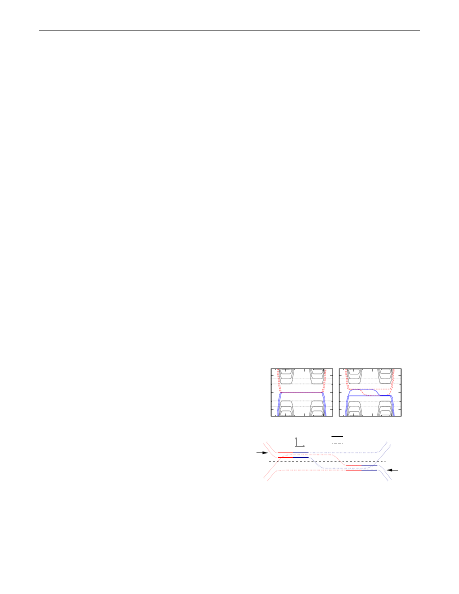
0.4
0.6
0.8
k/2
π
-0.05
0
0.05
E/t
0.4
0.6
0.8
k/2
π
(a)
(b)
L
µ
R
(c)
E
k
Bulk
Edge
Layer 2
Layer 1
FIG. 3 (color online).
Energy spectrum for a ribbon of bilayer
graphene with zigzag edges, t
?
=t 0:2, B 30 T, and width
N 400 unit cells: (a) eV 0; (b) eV t
?
=10. (c) Sketch of
the bands close to zero energy (for the biased bilayer) with
indication of bulk (solid lines) or edge (dotted lines) states and
their left (L) or right (R) positions along the ribbon.
Quasidegeneracies have been removed for clarity.
PRL 99, 216802 (2007)
P H Y S I C A L
R E V I E W
L E T T E R S
week ending
23 NOVEMBER 2007
216802-3
In our experimental case, n
0
> 0 and, therefore, the theory
works well for a wide range of electron doping n > 0,
whereas even a modest overall hole doping n < 0 corre-
sponds to a significant electrostatic difference between the
two graphene layers. In this case, the unscreened theory
overestimates the gap whereas the Hartree calculation
underestimates it. However, it is clear that the experimental
data in Fig.
interpolate between the screened result at
low hole doping and the unscreened one for high hole
densities. This indicates that the true gap actually lies
between
the
unscreened
and
screened
limits
[see
Fig.
], and that a more accurate treatment of screening
is needed when eV becomes of the order of t
?
.
In what follows, we model and discuss the QHE data
presented in Fig.
. We consider a ribbon of bilayer
graphene [
] with zigzag edges (armchair edges give
similar results). Figure
shows the energy spectrum in
the presence of a strong magnetic field. Figure
corre-
sponds to the unbiased case [see the curve labeled ‘‘pris-
tine,’’ Fig.
], where the four degenerate bands at zero
energy contain four degenerate bulk Landau levels [
] and
four surface states characteristic of the bilayer with zigzag
edges [
]. The spectrum for a biased device is shown in
Figure
. In this case two flat bands with energies
eV=2 and eV=2 appear, similar to the case of zero
magnetic field. The other two zero energy bands become
dispersive inside the gap, showing the band-crossing phe-
nomenon. The Landau level spacing is set by
3=2
p
ta=l
B
(l
B
is the magnetic length), and as long as
eV t
?
, the bias is much smaller than the Landau level
spacing at low fields. Then nonzero Landau levels in the
bulk are almost insensitive to V, as seen in Fig.
, except
for a small asymmetry between Dirac points. A close
inspection of Fig.
shows that the valley degeneracy is
lifted due to the different nature of the Landau states at K
and K
0
valleys with respect to their projection in each layer.
The valley asymmetry has a stronger effect in the zero
energy Landau levels, where the charge imbalance is satu-
rated. This opens a gap of eV in size. Also, there is an
intravalley degeneracy lifting [Fig.
], because only one
of the two Landau states of the unbiased system remains an
eigenstate when a bias is applied. For eV * t
?
(not shown
in Fig.
) the dispersive modes start crossing with nonzero
bulk Landau levels.
Let us now model the measured Hall conductivity for the
biased bilayer graphene, which is shown in the (red) curve
labeled doped in Fig.
. We consider the case of the
chemical potential lying inside the gap, between the last
hole- and the first electronlike bulk Landau levels, and
crossing the dispersive bands as shown in Fig.
. As
pointed out by Laughlin [
], changing the magnetic flux
through the ribbon loop by a flux quantum causes the states
to move rigidly towards one edge. In the usual integer
QHE, the energy increase due to this adiabatic flux varia-
tion results in the net transfer of n g electrons (spin and
valley degeneracy g) from one edge to the other, and the
quantization of the Hall conductivity follows the expres-
sion [
]:
I=V gne
2
=h
, where
I is the current carried
around the loop and
V the potential drop between the two
edges. However, in the present case there is no net charge
transfer across the ribbon. As seen in Fig.
, the band
states at the chemical potential belonging to the same band
are surface states localized at the same edge (see the figure
caption for details). The rigid movement of the states
towards one edge makes an electron-hole pair to appear
at both edges, resulting in zero net charge transfer.
Therefore, we expect a Hall plateau
xy
0 showing up
when the carriers change sign, i.e., at the neutrality point.
Accordingly, the Hall conductivity of the biased bilayer is
given by
xy
4Ne
2
=h
for all integer N, including zero.
Note that at the zero Hall plateau the current carried around
the ribbon loop is zero,
I 0, which implies, from the
theory view point, a diverging longitudinal resistivity at
low T, in stark contrast to all the other Hall plateaus that
exhibit zero
xx
, as in the standard QHE. This behavior has
been observed experimentally, as discussed above with
reference to Fig.
. This concludes our interpretation
of the experimental data.
E. V. C., N. M. R. P., and J. M. B. L. S. were supported by
POCI 2010 via Project No. PTDC/FIS/64404/2006 and
FCT through Grant No. SFRH/BD/13182/2003. F. G. was
supported by MEC (Spain) Grant No. FIS2005-05478-
C02-01 and EU Contract No. 12881 (NEST). A. H. C. N.
was supported through NSF Grant No. DMR-0343790. The
experimental work was supported by EPSRC (UK).
[1] K. S. Novoselov et al., Nature (London) 438, 197 (2005).
[2] Y. Zhang et al., Nature (London) 438, 201 (2005).
[3] K. S. Novoselov et al., Nature Phys. 2, 177 (2006).
[4] N. M. R. Peres, F. Guinea, and A. H. Castro Neto, Phys.
Rev. B 73, 125411 (2006).
[5] E. McCann and V. I. Fal’ko, Phys. Rev. Lett. 96, 086805
(2006).
[6] A. K. Geim and K. S. Novoselov, Nature Mater. 6, 183
(2007); J. Nilsson et al., Phys. Rev. B 76, 165416 (2007).
[7] Theory of the gap opening within the continuum model
was previously given by E. McCann, Phys. Rev. B 74,
161403 (2006).
[8] T. Ohta et al., Science 313, 951 (2006).
[9] K. S. Novoselov et al., Science 306, 666 (2004).
[10] F. Schedin et al., Nature Mater. 6, 652 (2007).
[11] F. Guinea, A. H. Castro Neto, and N. M. R. Peres, Phys.
Rev. B 73, 245426 (2006).
[12] E. V. Castro et al. (unpublished).
[13] The unbiased case, in the continuum approximation, was
studied in Ref. [
].
[14] R. B. Laughlin, Phys. Rev. B 23, 5632 (1981).
[15] B. I. Halperin, Phys. Rev. B 25, 2185 (1982).
PRL 99, 216802 (2007)
P H Y S I C A L
R E V I E W
L E T T E R S
week ending
23 NOVEMBER 2007
216802-4
Wyszukiwarka
Podobne podstrony:
32 Phys Rev Lett 98 196806 2007
25 Appl Rev Lett 91 233108 2007 Nieznany (2)
37 Phys Rev Lett 97 187401 2006
51 Phys Rev Lett 92 237001 2004
41 Phys Rev Lett 97 016801 2006
20 Phys Rev Lett 100 016602 2008
27 Phys Rev B 76 081406R 2007
57 Phys Rev B 67 054506 2003
11 Phys Rev B 78 085432 2008id Nieznany (2)
39 Phys Rev B 74 064403 2006
48 Phys Rev B 72 024537 2005
14 Phys Rev B 77 233406 2008
46 Phys Rev B 72 Rapid Commun 201401 2005
5 Phys Rev B 79 115441 2009
4 wykład0 24 10 2007
więcej podobnych podstron