
Plasmon spectroscopy of free-standing graphene films
T. Eberlein,
1
U. Bangert,
2
R. R. Nair,
2,4
R. Jones,
1
M. Gass,
3
A. L. Bleloch,
3
K. S. Novoselov,
4
A. Geim,
4
and P. R. Briddon
5
1
School of Physics, University of Exeter, Stocker Road, Exeter, EX4 4QL, United Kingdom
2
School of Materials, The University of Manchester, Manchester M1 7HS, United Kingdom
3
SuperSTEM Laboratories, CCLRC Daresbury Laboratory, Warrington WA4 4AD, United Kingdom
4
School of Physics and Astronomy, The University of Manchester, Manchester M1 7HS, United Kingdom
5
School of Natural Sciences, University of Newcastle upon Tyne, Newcastle upon Tyne NE1 7RU, United Kingdom
共Received 5 November 2007; revised manuscript received 25 January 2008; published 18 June 2008
兲
Plasmon spectroscopy of the thinnest possible membrane, a single layer of carbon atoms: graphene, has been
carried out in conjunction with ab initio calculations of the low loss function. We observe
and +-surface
plasmon modes in free-standing single sheets at 4.7 and 14.6 eV, which are substantially redshifted from their
values in graphite. These modes are in very good agreement with the theoretical spectra, which find the
- and
+ in-plane modes of graphene at 4.8 and 14.5 eV. We also find that there is little loss caused by out-of-plane
modes for energies less than about 10 eV.
DOI:
PACS number
共s兲: 73.20.⫺r, 81.05.Uw, 71.45.Gm, 79.20.Uv
There has recently been intense interest in the properties
of graphene
and, in particular, those properties that distin-
guish it from graphite. Among the many suggested areas
in
which graphene may excel is, e.g., its application for sensors
due to the sensitivity of its electronic structure to
adsorbates.
Low loss energy electron spectroscopy provides
a way of detecting changes in the electronic structure, which
are highly spatially resolved. To be able to employ this tech-
nique, the loss spectra of graphene and graphite must be
clearly understood.
From an experimental viewpoint, an essential task in the
research into two-dimensional
共2D兲 structures is to provide
evidence that they do indeed exist. This is especially impor-
tant because theory does not allow the existence of perfect
crystals in 2D space. The most conclusive evidence for the
existence of free-standing graphene has so far been obtained
from electron diffraction experiments
and all previously
published high resolution electron microscopy
共HREM兲 im-
ages, to our knowledge, are of bilayers. By carrying out
highly spatially resolved electron energy loss spectroscopy
共EELS兲, we observe specific redshifts in the frequency of
plasmons in sample positions concomitant with single
graphene sheets, very similar to those observed in single-
wall carbon nanotubes
共SWCNTs兲.
We also find further evi-
dence for existence of a single sheet by combining optical
and high angle annular dark field
共HAADF兲 imaging.
Surface plasmon behavior in thin metal sheets is well
documented experimentally and explained using dielectric
theory.
There are also numerous reports on surface plas-
mons in graphite and carbon nanotubes.
Plasmon behav-
ior of truly 2D graphite, i.e., of monolayer graphite foils has
been theoretically suggested in a number of papers
and
has been experimentally studied for flat monolayers grown
on TiC.
However, there has been, so far, no experimental
study for free-standing sheets. There have, however, been
studies of SWCNTs and much of the interpretation of plas-
mon behavior for SWCNTs for radius r
→⬁ can be applied
to free-standing single graphene sheets,
particularly as the
tubes are free standing also. A characteristic of thin foils is
the vanishing of the bulk plasmon mode, leaving only the
surface plasmon mode; the out-of-plane and in-plane contri-
butions of the latter split in energy when the product of
thickness d and momentum q, dq
→0; in graphite the maxi-
mum and/or minimum energy of the
→
ⴱ
transition tends
to roughly 7 and 5 eV and of the
→
ⴱ
transition to 20 and
15 eV, respectively.
The E field of a fast moving particle is elongated along its
direction of travel, therefore, when passing perpendicularly
through a graphene foil, mainly, the out-of plane mode with
momentum
បq parallel to E should be excited. However, as
shown below, these modes are forbidden in a single layer and
they have weak intensity in graphite. In an EELS experiment
carried out in a scanning transmission electron microscope
共STEM兲, although the momentum transfer is close to zero,
nonetheless, q has a considerable in-plane component be-
cause the collection angle is several millirad. For this reason,
we will observe those
surface and bulk plasmons excited
with q parallel to a.
Large graphene membranes were prepared by a microme-
chanical cleavage
of natural graphite on top of an oxidized
Si wafer. This deposition technique has the benefit of allow-
ing a quick and easy identification of mono- and multiple
layers by the additional optical contrast with respect to the
oxidized wafer. By using photolithography, a perforated
copper-gold film, serving as scaffold that could be used in
standard transmission electron microcopy holders, was de-
posited on top of the graphene crystallites. This scaffold was
lifted off the Si wafer, leaving the graphene attached to it.
Prior to electron microscopy, optical microscopy was used to
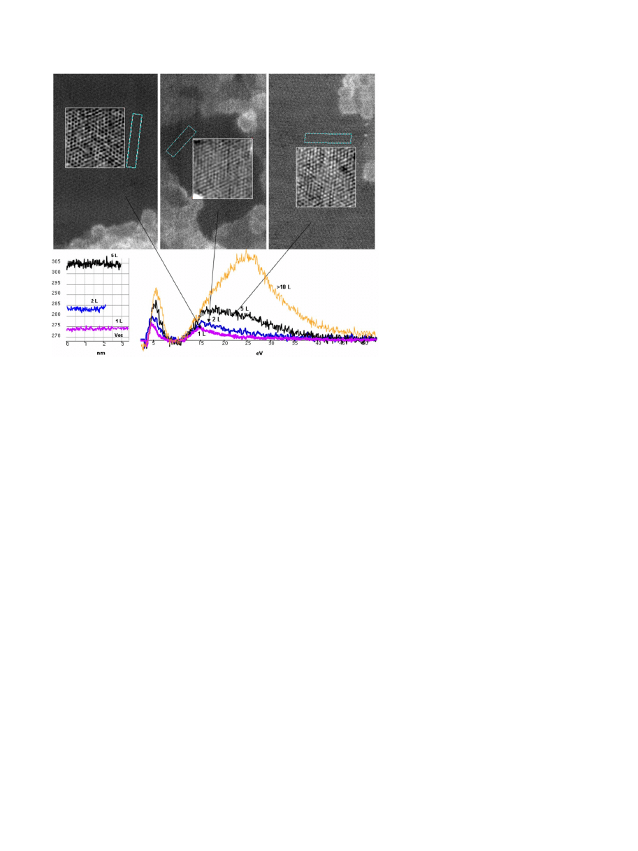
identify regions of one to few layers. HAADF images of
one-, two-, and five-layer regions are shown in Fig.
; the
rectangular boxes show the regions in which the intensity
关Fig.
兴, integrated over the width of the box, is traced.
The heights of the contrast profiles are multiples of the
smallest height measured in Fig.
, confirming that the
contrast in the dark region
关Fig.
兴 arises from one single
graphene sheet. Close inspection of the dark areas in each of
the images reveals uniform contrast upon which the hexago-
nal atomic lattice can be seen. Filtering of the HAADF im-
ages enhances the visibility of the lattice
关white-framed
boxes in Figs.
兴. The images are proof that the dark
areas are pristinely clean, i.e., free from contaminants.
PHYSICAL REVIEW B 77, 233406
共2008兲
1098-0121/2008/77
共23兲/233406共4兲
©2008 The American Physical Society
233406-1
The Daresbury aberration corrected SuperSTEM with an
Enfina EELS spectrometer was used for HREM bright field
and HAADF imaging in conjunction with EELS. EELS of
the plasmon region was carried out with a dispersion of 0.05
eV per channel at an energy resolution
共full width at half
maximum of the zero loss peak
兲 of 0.3–0.4 eV. The collec-
tion semiangle was approximately 19 mrad. The operating
voltage was 100 kV. In order to minimize beam damage, the
acquisition time per EEL spectrum was kept short
共⬃0.1 s兲;
the dose each pixel in a spectrum image received was
⬃1.6⫻10
7
electrons. When the acquisition time was in-
creased or when repeated scans were performed on the same
area, electron beam damage became manifest in formation of
point defects
共single and multiple vacancies兲.
In Fig.
, we show raw EEL data obtained by subtract-
ing the zero loss peak under identical conditions. The spectra
were all taken under the same acquisition conditions, hence,
direct comparison between them is possible.
The plasmon excitations in graphitic structures consist of
the
- and
+
plasmons both exhibiting bulk and surface
modes. In Fig.
, the plasmon spectra taken in clean
patches of one, two, five and multiple sheets shows that the
-mode, at 7 eV in graphite, has shifted to 4.7 eV in the
single layer. Furthermore, the spectrum here exhibits only
the
+
-surface mode at 14.6 eV and the 26 eV plasmon in
graphite is not present. The shape and intensity of the one-
layer plasmon structure was repeatedly measured in different
places on the same sample, in different samples, and even in
different experimental sessions. Given the same acquisition
conditions
共e.g., energy dispersion, electron beam current,
and dwell time
兲, nearly identical spectra were obtained,
which, at the same time, constituted the lowest plasmon sig-
nal measured overall. For two sheets, the triangular shape of
the
+
resonance shifts toward higher energies and the
integrated intensity under the peak
共between 10 and 40 eV兲
approximately doubles. A plateau between 15 and 20 eV
starts to appear, which becomes pronounced for increasing
numbers of sheets: In the five-layer patch features above 15
eV start to appear, the plasmon maximum keeps moving to
higher energies, accompanied by further broadening, and the
integrated intensity increases to
⬃5 times the value of the
single sheet. The plasmon structure for more than 10 sheets
strongly resembles that of the graphite. The plasmon charac-
teristics are, thus, supreme indicators for the presence of
single layers. However, the smallest amount of contamina-
tion, e.g., caused by individual molecular adsorbates, intro-
duces a “three-dimensional” component and leads to a break-
down of the 2D behavior, as is frequently evidenced.
Contaminants can easily be discerned in HREM and
HAADF images; in fact the whitish contrast bordering the
clean patches in the HAADF images Figs.
repre-
sent exactly this. We note that unlike low loss spectra, core
loss spectra were not found appropriate to reveal character-
istics that could help distinguish one layer from few layers
by their shape. In the spectrum of a larger number of
graphene sheets in Fig.
, resembling much that of a thin
graphitic slab, the well-known graphitic bulk
- and
-modes can be observed at 7 and 26 eV, respectively. We
have consistently observed
-plasmon behavior with distinct
occurrence of higher energy components, accompanied by a
step-wise increase in the HAADF intensity when going from
one to two or more sheets. Values of the HAADF intensity
for one, two, and more sheets
关see Fig.
兴 were measured
against the vacuum HAADF intensity and displayed incre-
ments of approximately integer multiples of the first incre-
ment above the vacuum intensity, i.e., the intensity of one
sheet. Data acquired from a number of experiments, carried
out on different samples and different days, yielded the same
results for the HAADF and the integrated EEL intensity.
The graphene plasmon behavior can be compared with
(a)
(b)
(c)
(d)
(e)
FIG. 1.
共Color online兲 共a兲–共c兲 HAADF
STEM images of ‘clean’ patches revealing
one, two, and five layers of graphene. The
area in the white-framed boxes has been sub-
jected to a low pass filter to disclose the atoms
more clearly: In the single layer the atoms in
the six rings are white and the hexagon center
is black.
共d兲 Intensity traces have been taken
along the long dimensions of the rectangular
cyan-framed boxes in
共a兲–共c兲; these traces
were then averaged over 40 pixels
共width of
boxes
兲. They show step-wise increase of the
HAADF intensity corresponding to the layer
number. The vacuum intensity is at
⬃268. 共e兲
EEL spectra of one, two, five and several lay-
ers of graphene showing the
-and the +
plasmon. The spectra are extracted from spec-
trum images; they are background subtracted
and each summed over 25 pixels.
BRIEF REPORTS
PHYSICAL REVIEW B 77, 233406
共2008兲
233406-2
that of thin carbon nanotubes, where the bulk plasmon sub-
sides and only tangential and radial surface modes prevail. A
trend has been observed for the
plasmon in tubes, where
r
/R− ⬎1,
namely, that the tangential
共or in plane兲 mode
increases on the expense of the radial
共or out of plane兲 and,
looking at Fig. 3
共a兲 in Ref.
, where plasmon spectra for
tubes with increasing r are presented, it furthermore appears
that for large r, only the tangential mode
共at ⬃15 eV兲 re-
mains, very similar to the graphene case. However, although
the resemblance with single-wall nanotube EEL data is large,
it cannot, from the start, be assumed that the graphene low
loss function reduces to the same theoretical approximation,
namely, to that derived for an electron passing in aloof
geometry.
For large tube diameters, in the work by Taverna
et al.,
the dielectric response tends to that of an anisotropic
thin foil in the weak coupling regime, however, in their case,
the electron passes parallel at a distance, whereas for a pen-
etrating geometry, as in our case, the potential would have to
be modified for electron transit within the foil. There has
been no expression of the low loss function derived using
dielectric theory and continuum models for the latter case.
Here, we derive the microscopic loss function for this sce-
nario via ab initio calculations.
These deal with supercells composed of carbon layers. We
imagine that the EELS experiment can be modeled by a
monochromatic beam of electrons whose momentum transfer
q to the sample is along either the c or a axis of the unit cell.
The unit cell contains planes of carbon atoms, which are
separated by multiples of the interlayer separation found in
graphite. Thus, to model graphene, layers of carbon atoms
are removed from the supercell leaving single layers well
separated from each other. Bilayers and trilayers can be mod-
eled by removing layers as before but leaving pairs of planes
with the separation and stacking sequence found in graphite
but each bilayer or trilayer is well separated from its neigh-
bor.
The rate at which energy and momentum h
q is lost from a
charged particle moving through a homogeneous dielectric
with speed
v due to ionization is proportional to the loss
function, which is the imaginary part of the inverse longitu-
dinal dielectric constant
ij
Within the random phase
the expression for
ij
is
ij
共q,E兲 =
␦
ij
+
冉
e
2
0
⍀
冊
兺
k
共r · i兲
k
v,k+qc
共r · j兲
k+qc,k
v
E
k+q,c
− E
k,
v
− E
.
Here, E
k,c
and E
k,
v
denote the empty and filled bands and Ω
is the volume of the unit cell. The sum is over a special set of
k vectors. For graphene and graphite, the principal values of
the loss tensor lie along c and a. This formulation includes
the effect of multiple inelastic scattering but assumes a ho-
mogeneous system. We use the AIMPRO local density func-
tional code
to evaluate the imaginary part of the dielectric
tensor for q = 0 and use the Kramers–Kronig relations to de-
rive its real part. We use 43 000 k-points and a broadening of
0.5 eV to fully converge the results. The loss function is then
found for graphite, graphene, and bimultilayers and trimulti-
layers.
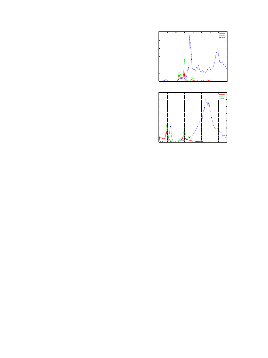
We first consider graphite. The top and bottom panels of
Fig.
show the loss function for q parallel to c and a
共blue
dotted-line spectra
兲, respectively. We find that the former has
peaks around 4, 12, 14, and 18 eV while the latter has a peak
at 7 eV and a broad peak at 27 eV. The 7 and 27 eV peaks are
due to
-electron plasmons
共one electron per atom兲 and
plus
共four electrons per atom兲 plasmons reflecting the van-
ishing of the real part of the dielectric constant.
The
⬃4 eV peak is due to a
to
ⴱ
transition. It is
noteworthy that the height of the
⬃4 eV peak is about 10%
of the height of the 7 eV peak and, hence, the main plasmon
loss below 10 eV is due to the plasmon moving along a.
These results are in reasonable agreement with studies of
the c and a plasmons in graphite:
Here, for q parallel to c,
peaks are observed at 4.6, 13, 15, and 19 eV but for q par-
allel to a, only peaks at 6.8 eV and a broad peak at 23 eV are
seen. Moreover, the intensity of the 4.6 eV peak is about
20% that of the 6.8 eV peak. This experiment shows that
energy loss in a transmission experiment, such as used here,
will be due to both q parallel to a and q parallel to c plas-
mons. The close agreement with the calculations suggests
that the loss function Im
共1/兲 is an appropriate way of mod-
eling the loss for planar sheets of graphite.
We now turn to graphene. This was modeled by expand-
ing the lattice parameter along c. The loss functions for q
parallel to c and a for 10 and 20 fold expansions are shown
in Fig.
as green dotted-line and red full-line spectra, re-
spectively. In the latter case where q is parallel to c
共top
panel
兲, the loss is almost zero up to 12 eV 共red line兲 and after
this the onset occurs at a similar energy to graphite. How-
ever, the peak heights are very different from graphite. The
0
0.5
1
1.5
2
2.5
3
0
5
10
15
20
25
30
35
40
q||c 20(c/a)
q||c 10(c/a)
q||c 1(c/a)
0
0.5
1
1.5
2
2.5
3
3.5
0
5
10
15
20
25
30
35
40
q||a 20(c/a)
q||a 10(c/a)
q||a 1(c/a)
FIG. 2.
共Color online兲 The loss function for graphite with a
separation between c-planes equal to 20 and 10 times its separation
in graphite and for graphite itself. Figure
共top兲 is case where q
储
c
and Fig.
共bottom兲 when q
储
a. Y axis: arbitrary units, x axis: energy
loss in eV.
BRIEF REPORTS
PHYSICAL REVIEW B 77, 233406
共2008兲
233406-3
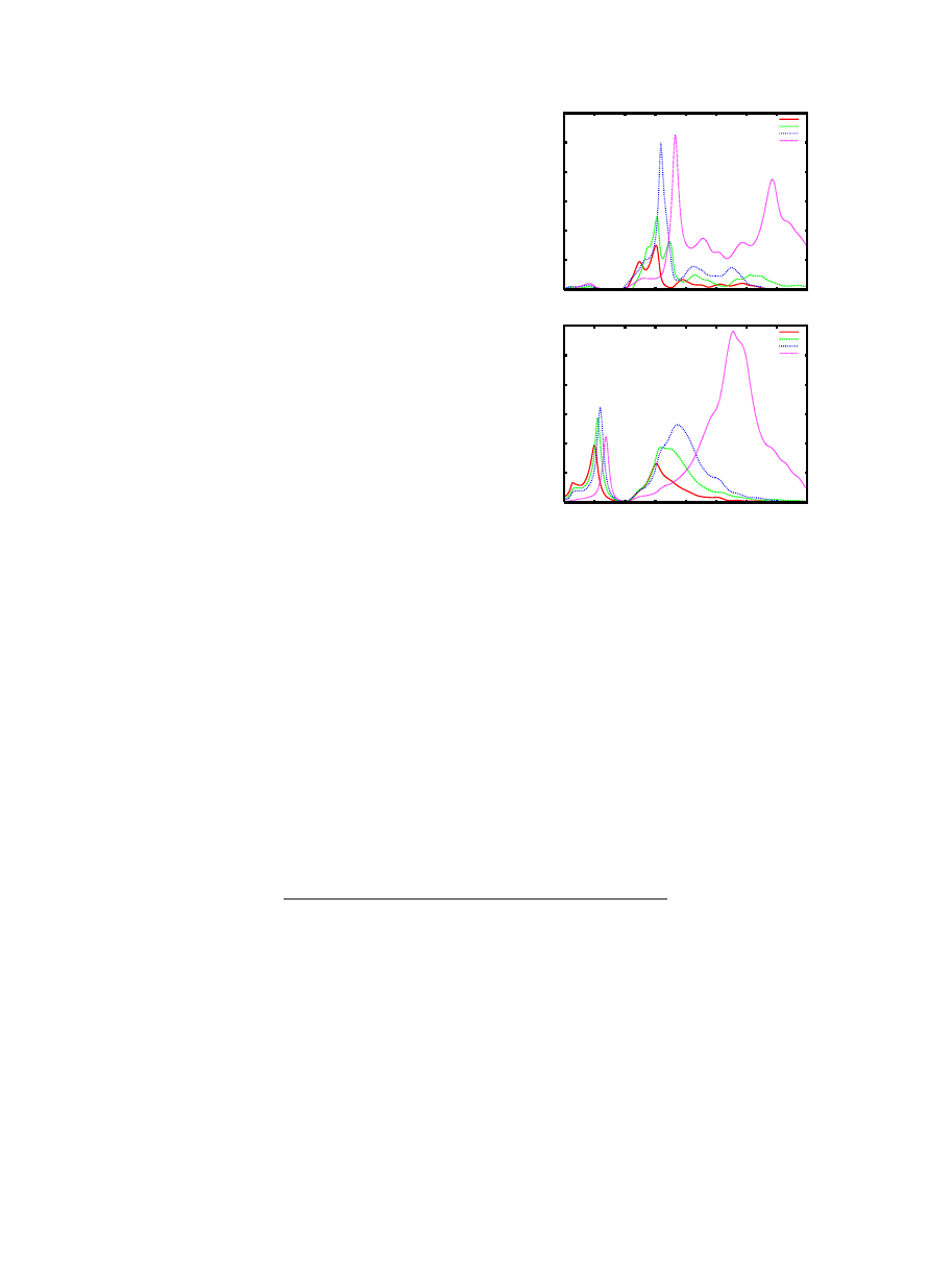
disappearance of the 4 eV peak can be explained by a selec-
tion rule. As stated above, the peak is due to a transition
between occupied
and unoccupied
ⴱ
bands at the M point
of the Brillouin zone. Inspection of the wave functions for
these two states shows that both transform as p
z
and are odd
under reflection symmetry present in the basal plane of
graphene but not AB graphite and, hence, the dipole matrix
element between them vanishes for transitions for which q is
parallel to c although the transition is allowed for q parallel
to a. This shows that the dielectric constant of graphene is
not the same as graphite.
Figure
, bottom panel, compares the loss function for q
parallel to a for graphene and graphite. We note there are
substantial redshifts of the peaks found in graphite.
The 7
eV
plasmon peak has shifted downward to about 4.8 eV
while the broad peak around 27 eV has sharpened and shifted
to below 15 eV. Such shifts are seen in the experimental
spectra shown in Fig.
We now investigate the loss functions for bilayers and
trilayers stacked as in graphite. The precise peak positions
depend on the separation of planes and to compare the loss
functions for graphite and multiple layers, we choose the
separation between periodically repeated multilayers to be 5
times the separation in graphite. We also use a broadening of
1.5 eV. The supercell containing the trilayer for example, has
three layers of graphene separated by the interlayer separa-
tion found in graphite, but the separation of these planes
from similar planes in adjacent unit cells along the c axis is
now five times the separation in graphite. The resulting loss
function is shown in Fig.
for single, double, and triple
layers, as well as for graphite. It is clear that there is an
increasing redshift of the peaks above, about 10 eV as the
number of layers decreases. The relative increase in ampli-
tudes of peaks for the different layers
共Fig.
, bottom panel
兲
seem roughly consistent with experimental spectra in Fig.
for one, two, and five layers but the observed spectra are
broader. All the layers except the single one show the out-
of-plane plasmon peak around 4 eV.
In conclusion, the 4.6 eV out-of-plane loss peak found in
graphite disappears for a single layer graphene. This is re-
lated to a selection rule operating in graphene but not in
graphite. This, however, does not occur for in-plane modes
or a graphene bilayer with AB stacking but does also occur
for a bilayer with AA stacking. It implies that any observa-
tions of a loss below 10 eV due to these plasmons must be
due to adsorbates lying on graphene and makes graphene
peculiarly sensitive to such adsorbates. We note that these
plasmons could be excited by light of grazing incidence and
polarized along c. A further feature, which is unique to the
plasmon behavior of graphene, is the shift of the 7 eV in-
plane plasmon seen in graphite to about 4.7 eV, as well as a
substantial redshift of the broad plasmon peak at 25 eV, seen
in graphite to about 14.6 eV in graphene accompanied by a
distinct shape change to skewed triangular. The redshifts de-
crease as the number of close-by layers increases.
1
K. S. Novoselov et al., Science 306, 666
共2004兲.
2
A. K. Geim and K. S. Novoselov, Nat. Mater. 6, 183
共2007兲.
3
F. Schedin et al., Nat. Mater. 6, 652
共2007兲.
4
C. J. Meyer et al., Nature
共London兲 446, 60 共2007兲.
5
O. Stéphan et al., Phys. Rev. B 66, 155422
共2002兲.
6
H. Raether, Phys. Thin Films 9, 149
共1977兲.
7
A. Otto, Phys. Status Solidi 22, 401
共1967兲.
8
J. F. Annett et al., Phys. Rev. B 37, 2408
共1988兲.
9
P. Laitenberger and R. E. Palmer, Phys. Rev. Lett. 76, 1952
共1996兲.
10
R. Perez and W. Que, J. Phys.: Condens. Matter 18, 3197
共2006兲.
11
M. Kociak et al., Phys. Rev. Lett. 87, 075501
共2001兲.
12
E. H. Hwang and S. Das Sarma, Phys. Rev. B 75, 205418
共2007兲.
13
A. G. Marinopoulos et al., Appl. Phys. A: Mater. Sci. Process.
78, 1157
共2004兲.
14
A. Nagashima et al., Solid State Commun. 83, 581
共1992兲.
15
R. R. Nair et al., Science
共to be published兲.
16
U. Bangert et al.
共unpublished兲.
17
M. H. Gass et al.
共unpublished兲.
18
D. Taverna et al., Phys. Rev. B 66, 235419
共2002兲.
19
P. Nozieres and D. Pines, Phys. Rev. 113, 1254
共1959兲.
20
H. Ehrenreich and M. H. Cohen, Phys. Rev. 115, 786
共1959兲.
21
S. L. Adler, Phys. Rev. 126, 413
共1962兲.
22
U. Bangert et al., Philos. Mag. 86, 4757
共2006兲.
23
K. Zeppenfeld, Phys. Lett. 25A, 335
共1967兲.
0
0.5
1
1.5
2
2.5
3
0
5
10
15
20
25
30
35
40
q||c single graphene
q||c bilayer graphene
q||c trilayer graphene
q||c graphite
0
0.5
1
1.5
2
2.5
3
0
5
10
15
20
25
30
35
40
q||a single graphene
q||a bilayer graphene
q||a trilayer graphene
q||a graphite
FIG. 3.
共Color online兲 Comparison of the loss function for a
single and multilayers of graphene for q
储
c
共top兲 and q
储
a
共bottom兲.
Note, the loss around 4 eV in the q
储
c case for the multilayer case
and its absence for single layer graphene
共shown as red line兲. Note
also the increasing redshift of the main peaks above about 10 eV as
the number of layers decreases. Y axis: arbitrary units, x axis: en-
ergy loss in eV.
BRIEF REPORTS
PHYSICAL REVIEW B 77, 233406
共2008兲
233406-4
Wyszukiwarka
Podobne podstrony:
20 Phys Rev Lett 100 016602 2008
57 Phys Rev B 67 054506 2003
Higiena ZOZ, Ust Zoz DzU07.14.89 skrót, Stan prawny: 2008-08-12
11 Phys Rev B 78 085432 2008id Nieznany (2)
39 Phys Rev B 74 064403 2006
48 Phys Rev B 72 024537 2005
24 Phys Rev Lett 99 216802 2007
27 Phys Rev B 76 081406R 2007
32 Phys Rev Lett 98 196806 2007
37 Phys Rev Lett 97 187401 2006
46 Phys Rev B 72 Rapid Commun 201401 2005
51 Phys Rev Lett 92 237001 2004
41 Phys Rev Lett 97 016801 2006
5 Phys Rev B 79 115441 2009
cwiczenia 14 28.03.2008, cwiczenia - dr skladowski
14 grudzień 2008 (2)
Zestaw 1 i 2 terma 14 04 2008
więcej podobnych podstron