SDLS030A − DECEMBER 1983 − REVISED NOVEMBER 2003
1
POST OFFICE BOX 655303
•
DALLAS, TEXAS 75265
D
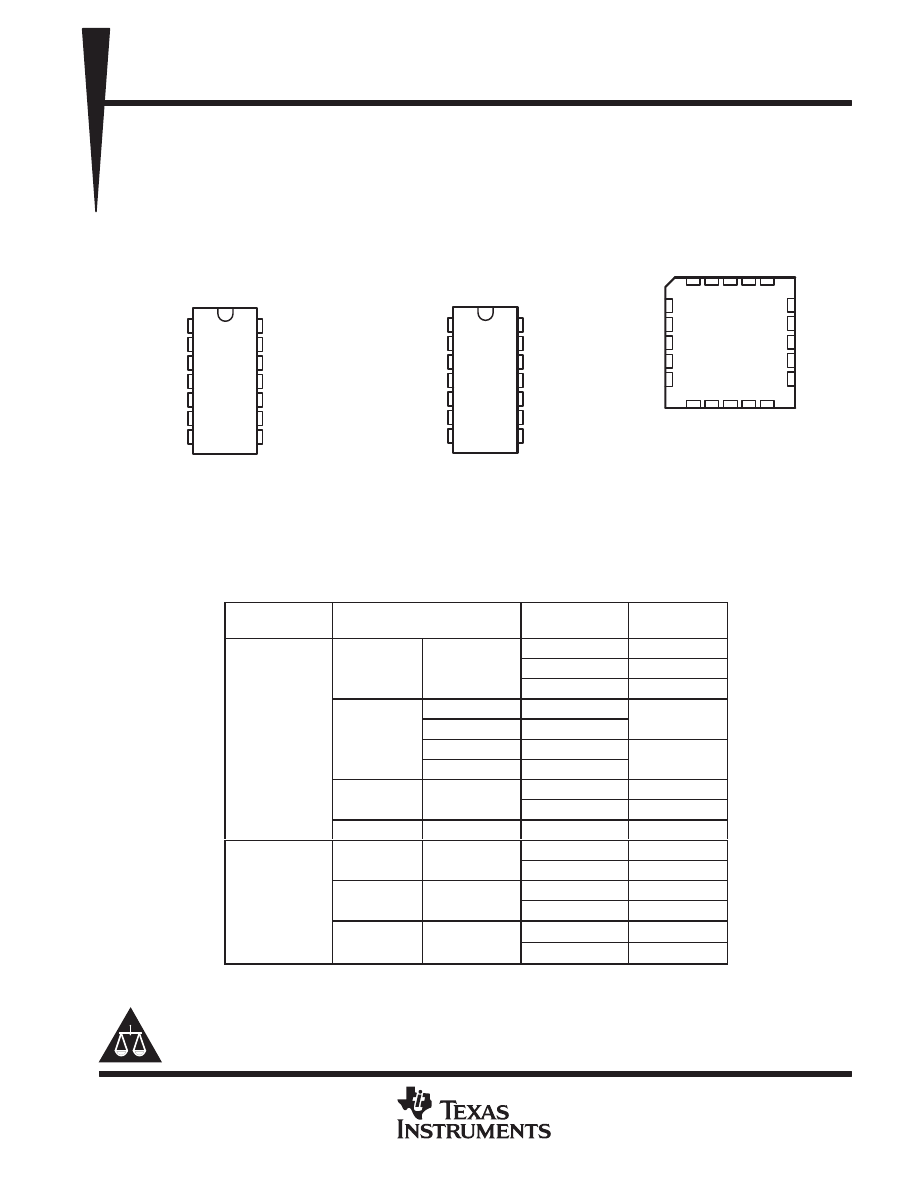
Package Options Include Plastic
Small-Outline (D, NS), Shrink Small-Outline
(DB), and Ceramic Flat (W) Packages,
Ceramic Chip Carriers (FK), and Standard
Plastic (N) and Ceramic (J) DIPs
D
Dependable Texas Instrument Quality and
Reliability
SN5405, SN54LS05, SN54S05 . . . J PACKAGE
SN7405 . . . N PACKAGE
SN74LS05 . . . D, DB, N, OR NS PACKAGE
SN74S05 . . . D, N, OR NS PACKAGE
(TOP VIEW)
1
2
3
4
5
6
7
14
13
12
11
10
9
8
1A
1Y
2A
2Y
3A
3Y
GND
V
CC
6A
6Y
5A
5Y
4A
4Y
3
2 1 20 19
9 10 11 12 13
4
5
6
7
8
18
17
16
15
14
6Y
NC
5A
NC
5Y
2A
NC
2Y
NC
3A
SN54LS05, SN54S05 . . . FK PACKAGE
(TOP VIEW)
1Y
1A
NC
4A
6A
3Y
GND
NC
CC
V
4Y
NC − No internal connection
SN54LS05, SN54S05 . . . W PACKAGE
(TOP VIEW)
1
2
3
4
5
6
7
14
13
12
11
10
9
8
1A
2Y
2A
V
CC
3A
3Y
4A
1Y
6A
6Y
GND
5Y
5A
4Y
description/ordering information
These devices contain six independent inverters. To perform correctly, the open-collector outputs require pullup
resistors. These devices may be connected to other open-collector outputs to implement active-low wired-OR
or active-high wire-AND functions. Open-collector devices often are used to generate high V
OH
levels.
ORDERING INFORMATION
TA
PACKAGE†
ORDERABLE
PART NUMBER
TOP-SIDE
MARKING
SN7405N
SN7405N
PDIP − N
Tube
SN74LS05N
SN74LS05N
PDIP − N
Tube
SN74S05N
SN74S05N
Tube
SN74LS05D
LS05
0
°
C to 70
°
C
SOIC − D
Tape and reel
SN74LS05DR
LS05
0
°
C to 70
°
C
SOIC − D
Tube
SN74S05D
S05
Tape and reel
SN74S05DR
S05
SOP − NS
Tape and reel
SN74LS05NSR
74LS05
SOP − NS
Tape and reel
SN74S05NSR
74S05
SSOP − DB
Tape and reel
SN74LS05DBR
LS05
CDIP − J
Tube
SNJ54LS05J
SNJ54LS05J
CDIP − J
Tube
SNJ54S05J
SNJ54S05J
−55
°
C to 125
°
C
CDIP − W
Tube
SNJ54LS05W
SNJ54LS05W
−55
°
C to 125
°
C
CDIP − W
Tube
SNJ54S05W
SNJ54S05W
LCCC − FK
Tube
SNJ54LS05FK
SNJ54LS05FK
LCCC − FK
Tube
SNJ54S05FK
SNJ54S05FK
† Package drawings, standard packing quantities, thermal data, symbolization, and PCB design
guidelines are available at www.ti.com/sc/package.
The SN5405 is obsolete
and no longer is supplied.
Copyright
2003, Texas Instruments Incorporated
! "#$ ! %#&'" ($)
(#"! " !%$""! %$ *$ $! $+! !#$!
!(( ,-) (#" %"$!!. ($! $"$!!'- "'#($
$!. '' %$$!)
Please be aware that an important notice concerning availability, standard warranty, and use in critical applications of
Texas Instruments semiconductor products and disclaimers thereto appears at the end of this data sheet.
%(#"! "%' /0121 '' %$$! $ $!$(
#'$!! *$,!$ $() '' *$ %(#"! %(#"
%"$!!. ($! $"$!!'- "'#($ $!. '' %$$!)
SDLS030A − DECEMBER 1983 − REVISED NOVEMBER 2003
2
POST OFFICE BOX 655303
•
DALLAS, TEXAS 75265
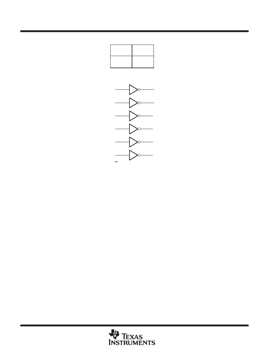
FUNCTION TABLE
(each inverter)
INPUT
OUTPUT
INPUT
A
OUTPUT
Y
H
L
L
H
logic diagram (positive logic)
1A
2A
3A
4A
5A
6A
1Y
2Y
3Y
4Y
5Y
6Y
1
3
5
9
11
13
2
4
6
8
10
12
Y = A
Pin numbers shown are for the D, DB, J, N, and NS packages.
The SN5405 is obsolete
and no longer is supplied.
SDLS030A − DECEMBER 1983 − REVISED NOVEMBER 2003
3
POST OFFICE BOX 655303
•
DALLAS, TEXAS 75265
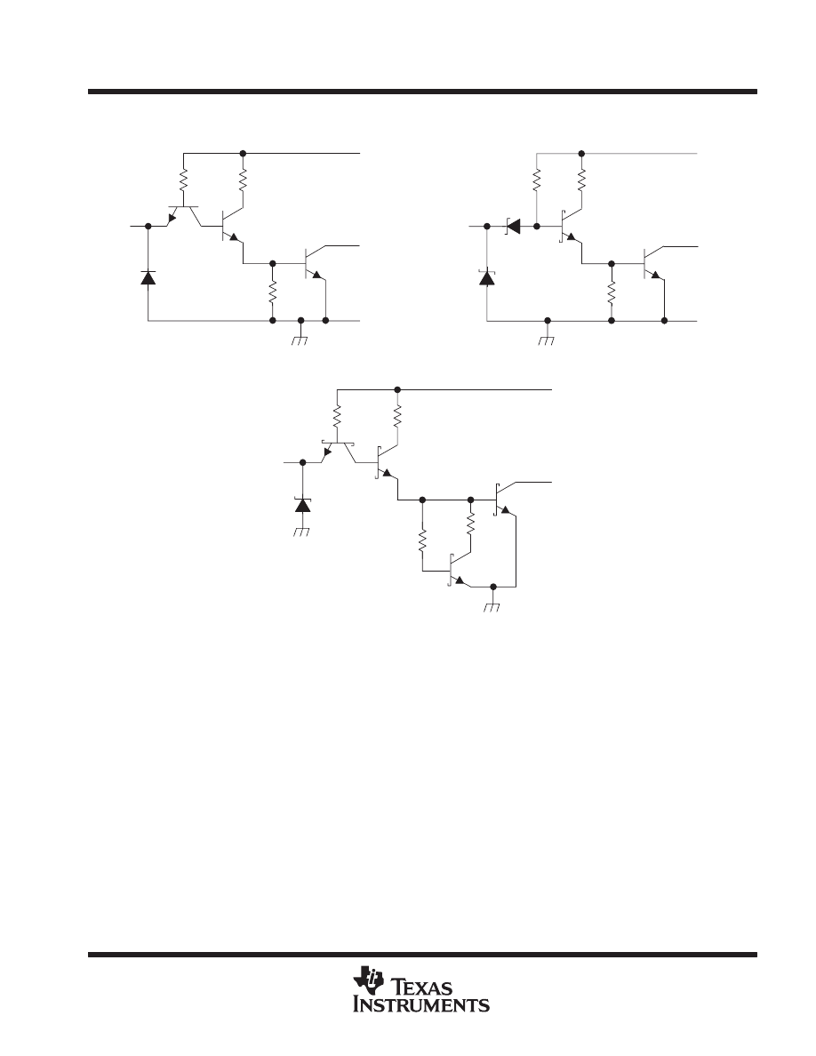
schematic (each inverter)
Resistor values shown are nominal.
4 k
Ω
Input
A
Output
Y
GND
VCC
1.6 k
Ω
1 k
Ω
’05
20 k
Ω
Input
A
Output
Y
VCC
8 k
Ω
4.5 k
Ω
’LS05
GND
2.8 k
Ω
Output
Y
VCC
900
Ω
500
Ω
’S05
Input
A
250
Ω
absolute maximum ratings over operating free-air temperature (unless otherwise noted)
†
Supply voltage, V
CC
(see Note 1): ’05, ’LS05, ’S05
7 V
. . . . . . . . . . . . . . . . . . . . . . . . . . . . . . . . . . . . . . . . . . . . . .
Input voltage, V
I
: ’05, ’S05
5.5 V
. . . . . . . . . . . . . . . . . . . . . . . . . . . . . . . . . . . . . . . . . . . . . . . . . . . . . . . . . . . . . . . . .
’LS05
7 V
. . . . . . . . . . . . . . . . . . . . . . . . . . . . . . . . . . . . . . . . . . . . . . . . . . . . . . . . . . . . . . . . . . . . . .
Off-state output voltage, V
O
7 V
. . . . . . . . . . . . . . . . . . . . . . . . . . . . . . . . . . . . . . . . . . . . . . . . . . . . . . . . . . . . . . . . . .
Package thermal impedance,
θ
JA
(see Note 2): D package
86
°
C/W
. . . . . . . . . . . . . . . . . . . . . . . . . . . . . . . . . . .
DB package
96
°
C/W
. . . . . . . . . . . . . . . . . . . . . . . . . . . . . . . . .
N package
80
°
C/W
. . . . . . . . . . . . . . . . . . . . . . . . . . . . . . . . . . .
NS package
76
°
C/W
. . . . . . . . . . . . . . . . . . . . . . . . . . . . . . . . .
Storage temperature range, T
stg
−65
°
C to 150
°
C
. . . . . . . . . . . . . . . . . . . . . . . . . . . . . . . . . . . . . . . . . . . . . . . . . . .
† Stresses beyond those listed under “absolute maximum ratings” may cause permanent damage to the device. These are stress ratings only, and
functional operation of the device at these or any other conditions beyond those indicated under “recommended operating conditions” is not
implied. Exposure to absolute-maximum-rated conditions for extended periods may affect device reliability.
NOTES:
1. Voltage values are with respect to network ground terminal.
2. The package thermal impedance is calculated in accordance with JESD 51-7.
The SN5405 is obsolete
and no longer is supplied.
SDLS030A − DECEMBER 1983 − REVISED NOVEMBER 2003
4
POST OFFICE BOX 655303
•
DALLAS, TEXAS 75265
recommended operating conditions
SN5405
SN7405
UNIT
MIN
NOM
MAX
MIN
NOM
MAX
UNIT
VCC
Supply voltage
4.5
5
5.5
4.75
5
5.25
V
VIH
High-level input voltage
2
2
V
VIL
Low-level input voltage
0.8
0.8
V
VOH
High-level output voltage
5.5
5.5
V
IOL
Low-level output current
16
16
mA
TA
Operating free-air temperature
−55
125
0
70
°
C
electrical characteristics over recommended operating free-air temperature range (unless
otherwise noted)
PARAMETER
TEST CONDITIONS†
SN5405
SN7405
UNIT
PARAMETER
TEST CONDITIONS†
MIN
TYP‡
MAX
MIN
TYP‡
MAX
UNIT
VIK
VCC = MIN,
II = −12 mA
−1.5
−1.5
V
IOH
VCC = MIN,
VOH = 5.5 V
VIL = 0.8 V
0.25
mA
IOH
VCC = MIN,
VOH = 5.5 V
VIL = 0.7 V
0.25
mA
VOL
VCC = MIN,
VIH = 2 V,
IOL = 16 mA
0.2
0.4
0.2
0.4
V
II
VCC = MAX,
VI = 5.5 V
1
1
mA
IIH
VCC = MAX,
VI = 2.4 V
40
40
µ
A
IIL
VCC = MAX,
VI = 0.4 V
−1.6
−1.6
mA
ICCH
VCC = MAX,
VI = 0 V
6
12
6
12
mA
ICCL
VCC = MAX,
VI = 4.5 V
18
33
18
33
mA
† For conditions shown as MIN or MAX, use the appropriate value specified under recommended operating conditions.
‡ All typical values are at VCC = 5 V, TA = 25
°
C.
switching characteristics, V
CC
= 5 V, T
A
= 25
°
C (see Figure 1)
PARAMETER
FROM
(INPUT)
TO
(OUTPUT)
TEST CONDITIONS
MIN
TYP
MAX
UNIT
tPLH
A
Y
RL = 4 k
Ω
CL = 15 pF
40
55
ns
tPHL
A
Y
RL = 400
Ω
CL = 15 pF
8
15
ns
The SN5405 is obsolete
and no longer is supplied.
SDLS030A − DECEMBER 1983 − REVISED NOVEMBER 2003
5
POST OFFICE BOX 655303
•
DALLAS, TEXAS 75265
recommended operating conditions
SN54LS05
SN74LS05
UNIT
MIN
NOM
MAX
MIN
NOM
MAX
UNIT
VCC
Supply voltage
4.5
5
5.5
4.75
5
5.25
V
VIH
High-level input voltage
2
2
V
VIL
Low-level input voltage
0.7
0.8
V
VOH
High-level output voltage
5.5
5.5
V
IOL
Low-level output current
4
8
mA
TA
Operating free-air temperature
−55
125
0
70
°
C
electrical characteristics over recommended operating free-air temperature range (unless
otherwise noted)
PARAMETER
TEST CONDITIONS†
SN54LS05
SN74LS05
UNIT
PARAMETER
TEST CONDITIONS†
MIN
TYP‡
MAX
MIN
TYP‡
MAX
UNIT
VIK
VCC = MIN,
II = −18 mA
−1.5
−1.5
V
IOH
VCC = MIN,
VIL = MAX,
VOH = 5.5 V
0.1
0.1
mA
VOL
VCC = MIN,
VIH = 2 V
IOL = 4 mA
0.25
0.4
0.25
0.4
V
VOL
VCC = MIN,
VIH = 2 V
IOL = 8 mA
0.35
0.5
V
II
VCC = MAX,
VI = 7 V
0.1
0.1
mA
IIH
VCC = MAX,
VI = 2.7 V
20
20
µ
A
IIL
VCC = MAX,
VI = 0.4 V
−0.4
−0.4
mA
ICCH
VCC = MAX,
VI = 0 V
1.2
2.4
1.2
2.4
mA
ICCL
VCC = MAX,
VI = 4.5 V
3.6
6.6
3.6
6.6
mA
† For conditions shown as MIN or MAX, use the appropriate value specified under recommended operating conditions.
‡ All typical values are at VCC = 5 V, TA = 25
°
C.
switching characteristics, V
CC
= 5 V, T
A
= 25
°
C (see Figure 2)
PARAMETER
FROM
(INPUT)
TO
(OUTPUT)
TEST CONDITIONS
MIN
TYP
MAX
UNIT
tPLH
A
Y
RL = 2 k
Ω
,
CL = 15 pF
17
32
ns
tPHL
A
Y
RL = 2 k
Ω
,
CL = 15 pF
15
28
ns
The SN5405 is obsolete
and no longer is supplied.
SDLS030A − DECEMBER 1983 − REVISED NOVEMBER 2003
6
POST OFFICE BOX 655303
•
DALLAS, TEXAS 75265
recommended operating conditions
SN54S05
SN74S05
UNIT
MIN
NOM
MAX
MIN
NOM
MAX
UNIT
VCC
Supply voltage
4.5
5
5.5
4.75
5
5.25
V
VIH
High-level input voltage
2
2
V
VIL
Low-level input voltage
0.8
0.8
V
VOH
High-level output voltage
5.5
5.5
V
IOL
Low-level output current
20
20
mA
TA
Operating free-air temperature
−55
125
0
70
°
C
electrical characteristics over recommended operating free-air temperature range (unless
otherwise noted)
PARAMETER
TEST CONDITIONS†
SN54S05
SN74S05
UNIT
PARAMETER
TEST CONDITIONS†
MIN
TYP‡
MAX
MIN
TYP‡
MAX
UNIT
VIK
VCC = MIN,
II = −18 mA
−1.2
−1.2
V
IOH
VCC = MIN,
VOH = 5.5 V
VIL = 0.8 V
0.25
mA
IOH
VCC = MIN,
VOH = 5.5 V
VIL = 0.7 V
0.25
mA
VOL
VCC = MIN,
VIH = 2 V,
IOL = 20 mA
0.5
0.5
V
II
VCC = MAX,
VI = 5.5 V
1
1
mA
IIH
VCC = MAX,
VI = 2.7 V
50
50
µ
A
IIL
VCC = MAX,
VI = 0.5 V
−2
−2
mA
ICCH
VCC = MAX,
VI = 0 V
9
19.8
9
19.8
mA
ICCL
VCC = MAX,
VI = 4.5 V
30
54
30
54
mA
† For conditions shown as MIN or MAX, use the appropriate value specified under recommended operating conditions.
‡ All typical values are at VCC = 5 V, TA = 25
°
C.
switching characteristics, V
CC
= 5 V, T
A
= 25
°
C (see Figure 1)
PARAMETER
FROM
(INPUT)
TO
(OUTPUT)
TEST CONDITIONS
MIN
TYP
MAX
UNIT
tPLH
CL = 15 pF
2
5
7.5
ns
tPHL
A
Y
RL = 280
Ω
CL = 15 pF
2
4.5
7
ns
tPLH
A
Y
RL = 280
Ω
CL = 50 pF
7.5
ns
tPHL
CL = 50 pF
7
ns
The SN5405 is obsolete
and no longer is supplied.
SDLS030A − DECEMBER 1983 − REVISED NOVEMBER 2003
7
POST OFFICE BOX 655303
•
DALLAS, TEXAS 75265
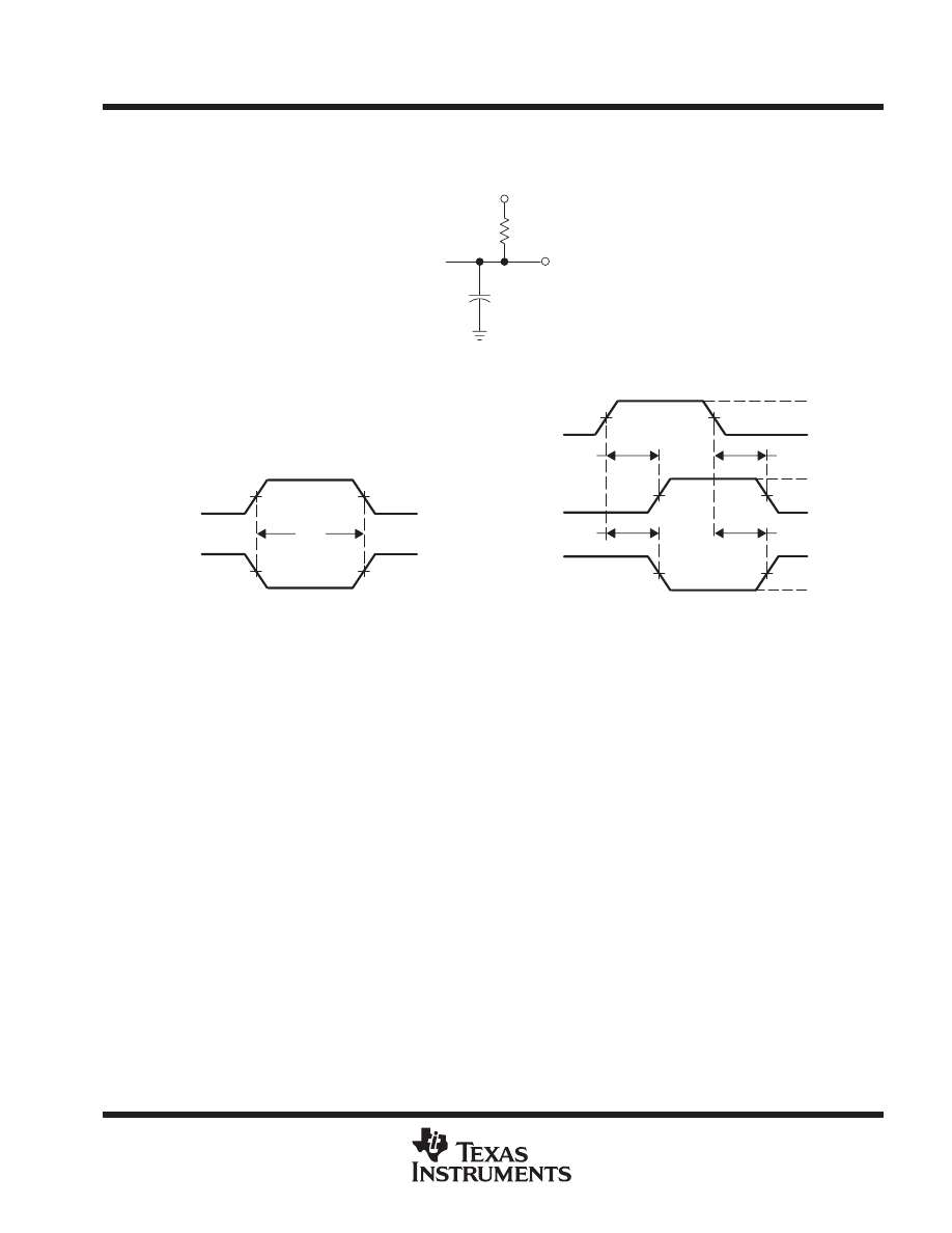
PARAMETER MEASUREMENT INFORMATION
SERIES 54/74 AND 54S/74S DEVICES
From Output
Under Test
CL
(see Note A)
RL
Test Point
VCC
LOAD CIRCUIT
1.5 V
1.5 V
High-Level
Pulse
1.5 V
1.5 V
tw
Low-Level
Pulse
VOLTAGE WAVEFORMS
PULSE WIDTHS
NOTES: A. CL includes probe and jig capacitance.
B. In the examples above, the phase relationships between inputs and outputs have been chosen arbitrarily.
C. All input pulses are supplied by generators having the following characteristics: PRR
≤
1 MHz, ZO = 50
Ω
, and:
For Series 54/74, tr
≤
7 ns, tf
≤
7 ns.
For Series 54S/74S, tr
≤
2.5 ns, tf
≤
2.5 ns.
D. The outputs are measured one at a time with one input transition per measurement.
1.5 V
1.5 V
Input
tPLH
In-Phase
Output
3 V
0 V
1.5 V
1.5 V
VOH
VOL
tPHL
1.5 V
1.5 V
VOH
VOL
tPHL
tPLH
Out-of-Phase
Output
VOLTAGE WAVEFORMS
PROPAGATION DELAY TIMES
Figure 1. Load Circuit and Voltage Waveforms
The SN5405 is obsolete
and no longer is supplied.
SDLS030A − DECEMBER 1983 − REVISED NOVEMBER 2003
8
POST OFFICE BOX 655303
•
DALLAS, TEXAS 75265
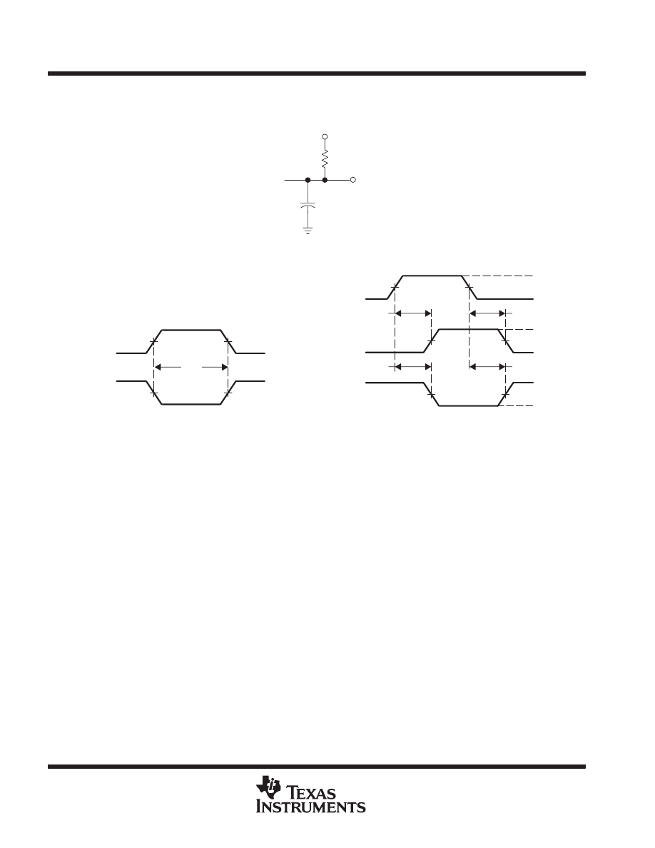
PARAMETER MEASUREMENT INFORMATION
SERIES 54LS/74LS DEVICES
From Output
Under Test
CL
(see Note A)
RL
Test Point
VCC
LOAD CIRCUIT
1.3 V
1.3 V
High-Level
Pulse
1.3 V
1.3 V
tw
Low-Level
Pulse
VOLTAGE WAVEFORMS
PULSE WIDTHS
NOTES: A. CL includes probe and jig capacitance.
B. In the examples above, the phase relationships between inputs and outputs have been chosen arbitrarily.
C. All input pulses are supplied by generators having the following characteristics: PRR
≤
1 MHz, ZO = 50
Ω
, tr
≤
1.5 ns, tf
≤
2.6 ns.
D. The outputs are measured one at a time with one input transition per measurement.
1.3 V
1.3 V
Input
tPLH
In-Phase
Output
3 V
0 V
1.3 V
1.3 V
VOH
VOL
tPHL
1.3 V
1.3 V
VOH
VOL
tPHL
tPLH
Out-of-Phase
Output
VOLTAGE WAVEFORMS
PROPAGATION DELAY TIMES
Figure 2. Load Circuit and Voltage Waveforms
The SN5405 is obsolete
and no longer is supplied.
Wyszukiwarka
Podobne podstrony:
7405
7405
praca-magisterska-7405, Dokumenty(2)
7405
7405
7405
7405
więcej podobnych podstron