M54HC05
M74HC05
February 1993
HEX INVERTER (OPEN DRAIN)
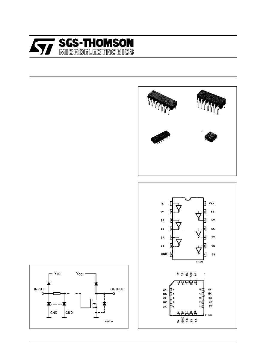
B1R
(Plastic Package)
ORDER CODES :
M54HC05F1R
M74HC05M1R
M74HC05B1R
M74HC05C1R
F1R
(Ceramic Package)
M1R
(Micro Package)
C1R
(Chip Carrier)
PIN CONNECTIONS (top view)
NC =
No Internal
Connection
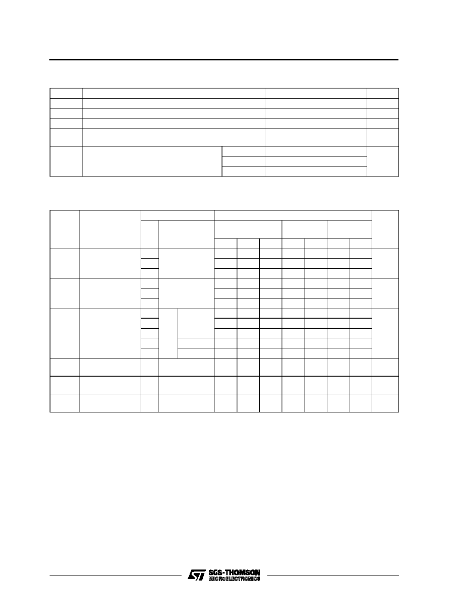
INPUT AND OUTPUT EQUIVALENT CIRCUIT
.
HIGH SPEED
t
PD
= 8 ns (TYP.) AT V
CC
= 5 V
.
LOW POWER DISSIPATION
I
CC
= 1
µ
A (MAX.) AT T
A
= 25
°
C
.
HIGH NOISE IMMUNITY
V
NIH
= V
NIL
= 28 % V
CC
(MIN.)
.
OUTPUT DRIVE CAPABILITY
10 LSTTL LOADS
.
WIDE OPERATING VOLTAGE RANGE
V
CC
(OPR) = 2 V TO 6 V
.
PIN AND FUNCTION COMPATIBLE WITH
54/74LS05
The M54/74HC05 is a high speed CMOS HEX
OPEN DRAIN INVERTER fabricated in silicon gate
C
2
MOS technology. It has the same high speed per-
formance of LSTTL combined with true CMOS low
power consumption.
The internal circuit is composed of 3 stages includ-
ing buffer output, which enables high noise im-
munity and stable output. All inputs are equipped
with circuits against static discharge and transient
excess voltage.
DESCRIPTION
1/9
TRUTH TABLE
A
Y
L
Z
H
L
Z = High impedance
PIN DESCRIPTION
PIN No
SYMBOL
NAME AND FUNCTION
1, 3, 5, 9,
11, 13
1A to 6A
Data Inputs
2, 4, 6, 8,
10, 12
1Y to 6Y
Data Outputs
7
GND
Ground (0V)
14
V
CC
Positive Supply Voltage
IEC LOGIC SYMBOL
LOGIC DIAGRAM (Per Gate)
ABSOLUTE MAXIMUM RATINGS
Symbol
Parameter
Value
Unit
V
CC
Supply Voltage
-0.5 to +7
V
V
I
DC Input Voltage
-0.5 to V
CC
+ 0.5
V
V
O
DC Output Voltage
-0.5 to V
CC
+ 0.5
V
I
IK
DC Input Diode Current
±
20
mA
I
OK
DC Output Diode Current
±
20
mA
I
O
DC Output Sink Current Per Output Pin
25
mA
I
CC
or I
GND
DC V
CC
or Ground Current
±
50
mA
P
D
Power Dissipation
500 (*)
mW
T
stg
Storage Temperature
-65 to +150
o
C
T
L
Lead Temperature (10 sec)
300
o
C
Absolute Maximum Ratings are those values beyond which damage to the device may occur. Functional operation under these condition is not implied.
(*) 500 mW:
≅
65
o
C derate to 300 mW by 10mW/
o
C: 65
o
C to 85
o
C
M54/M74HC05
2/9
RECOMMENDED OPERATING CONDITIONS
Symbol
Parameter
Value
Unit
V
CC
Supply Voltage
2 to 6
V
V
I
Input Voltage
0 to V
CC
V
V
O
Output Voltage
0 to V
CC
V
T
op
Operating Temperature: M54HC Series
M74HC Series
-55 to +125
-40 to +85
o
C
o
C
t
r
, t
f
Input Rise and Fall Time
V
CC
= 2 V
0 to 1000
ns
V
CC
= 4.5 V
0 to 500
V
CC
= 6 V
0 to 400
DC SPECIFICATIONS
Symbol
Parameter
Test Conditions
Value
Unit
V
CC
(V)
T
A
= 25
o
C
54HC and 74HC
-40 to 85
o
C
74HC
-55 to 125
o
C
54HC
Min.
Typ.
Max.
Min.
Max.
Min.
Max.
V
IH
High Level Input
Voltage
2.0
1.5
1.5
1.5
V
4.5
3.15
3.15
3.15
6.0
4.2
4.2
4.2
V
IL
Low Level Input
Voltage
2.0
0.5
0.5
0.5
V
4.5
1.35
1.35
1.35
6.0
1.8
1.8
1.8
V
OL
Low Level Output
Voltage
2.0
V
I
=
V
IH
or
V
IL
I
O
= 20
µ
A
0.0
0.1
0.1
0.1
V
4.5
0.0
0.1
0.1
0.1
6.0
0.0
0.1
0.1
0.1
4.5
I
O
= 4.0 mA
0.17
0.26
0.33
0.40
6.0
I
O
= 5.2 mA
0.18
0.26
0.33
0.40
I
I
Input Leakage
Current
6.0
V
I
= V
CC
or GND
±
0.1
±
1
±
1
µ
A
I
OZ
Output Leakage
Current
6.0
V
I
= V
IH
or V
IL
V
O
= V
CC
or GND
±
0.5
±
5
±
10
µ
A
I
CC
Quiescent Supply
Current
6.0
V
I
= V
CC
or GND
1
10
20
µ
A
M54/M74HC05
3/9
AC ELECTRICAL CHARACTERISTICS (C
L
= 50 pF, Input t
r
= t
f
= 6 ns)
Symbol
Parameter
Test Conditions
Value
Unit
V
CC
(V)
T
A
= 25
o
C
54HC and 74HC
-40 to 85
o
C
74HC
-55 to 125
o
C
54HC
Min.
Typ.
Max.
Min.
Max.
Min.
Max.
t
THL
Output Transition
Time
2.0
30
75
95
110
ns
4.5
8
15
19
22
6.0
7
13
16
19
t
PLZ
Propagation
Delay Time
2.0
R
L
= 1K
Ω
20
90
115
135
ns
4.5
11
18
23
27
6.0
10
15
20
23
t
PZL
Propagation
Delay Time
2.0
R
L
= 1K
Ω
33
90
115
135
ns
4.5
9
18
23
27
6.0
8
15
20
23
C
IN
Input Capacitance
5
10
10
10
pF
C
OUT
Output
Capacitance
10
pF
C
PD
(*)
Power Dissipation
Capacitance
6.5
pF
(*) C
PD
is defined as the value of the IC’s internal equivalent capacitance which is calculated from the operating current consumption without load.
M54/M74HC05
4/9
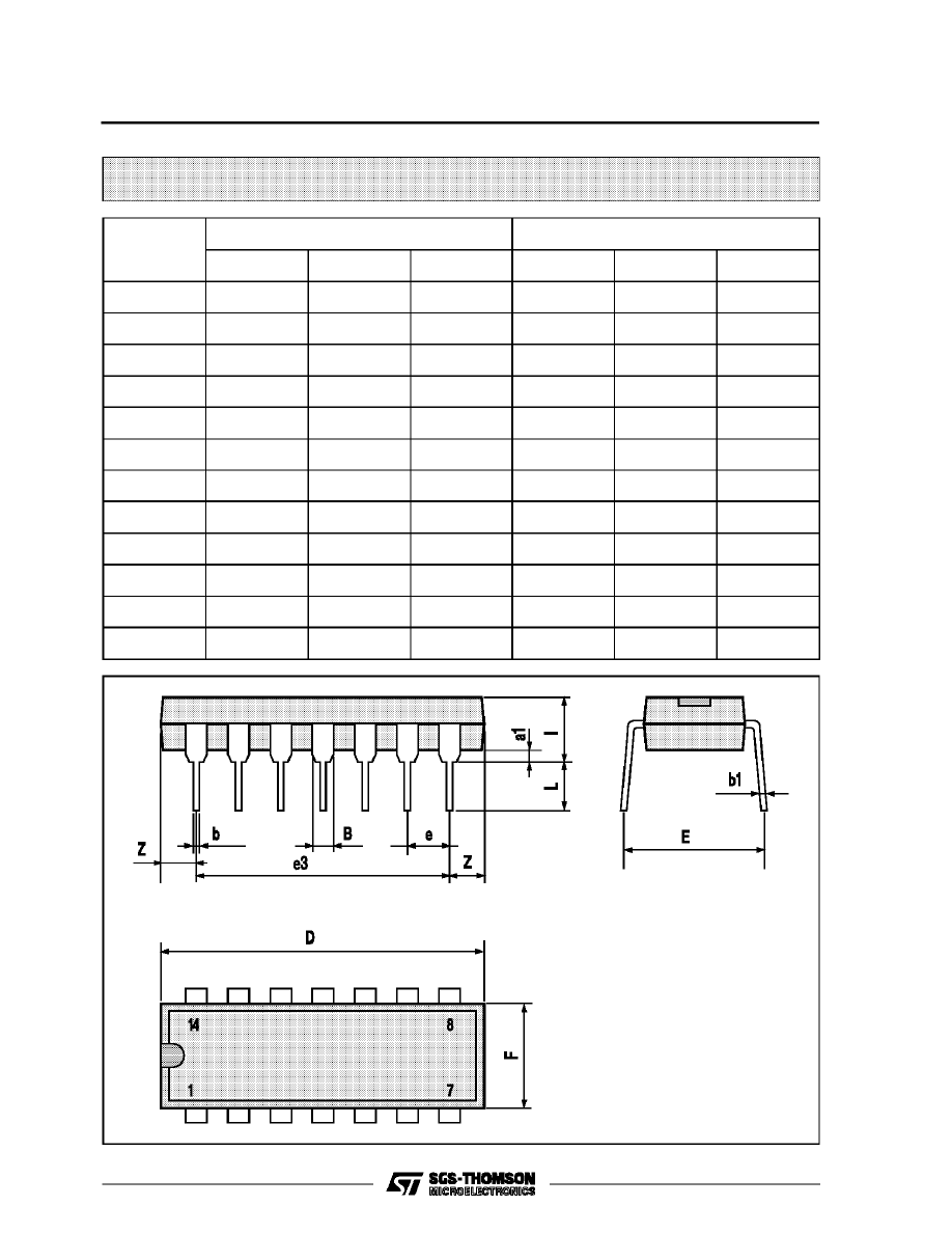
Plastic DIP14 MECHANICAL DATA
DIM.
mm
inch
MIN.
TYP.
MAX.
MIN.
TYP.
MAX.
a1
0.51
0.020
B
1.39
1.65
0.055
0.065
b
0.5
0.020
b1
0.25
0.010
D
20
0.787
E
8.5
0.335
e
2.54
0.100
e3
15.24
0.600
F
7.1
0.280
I
5.1
0.201
L
3.3
0.130
Z
1.27
2.54
0.050
0.100
P001A
M54/M74HC05
5/9
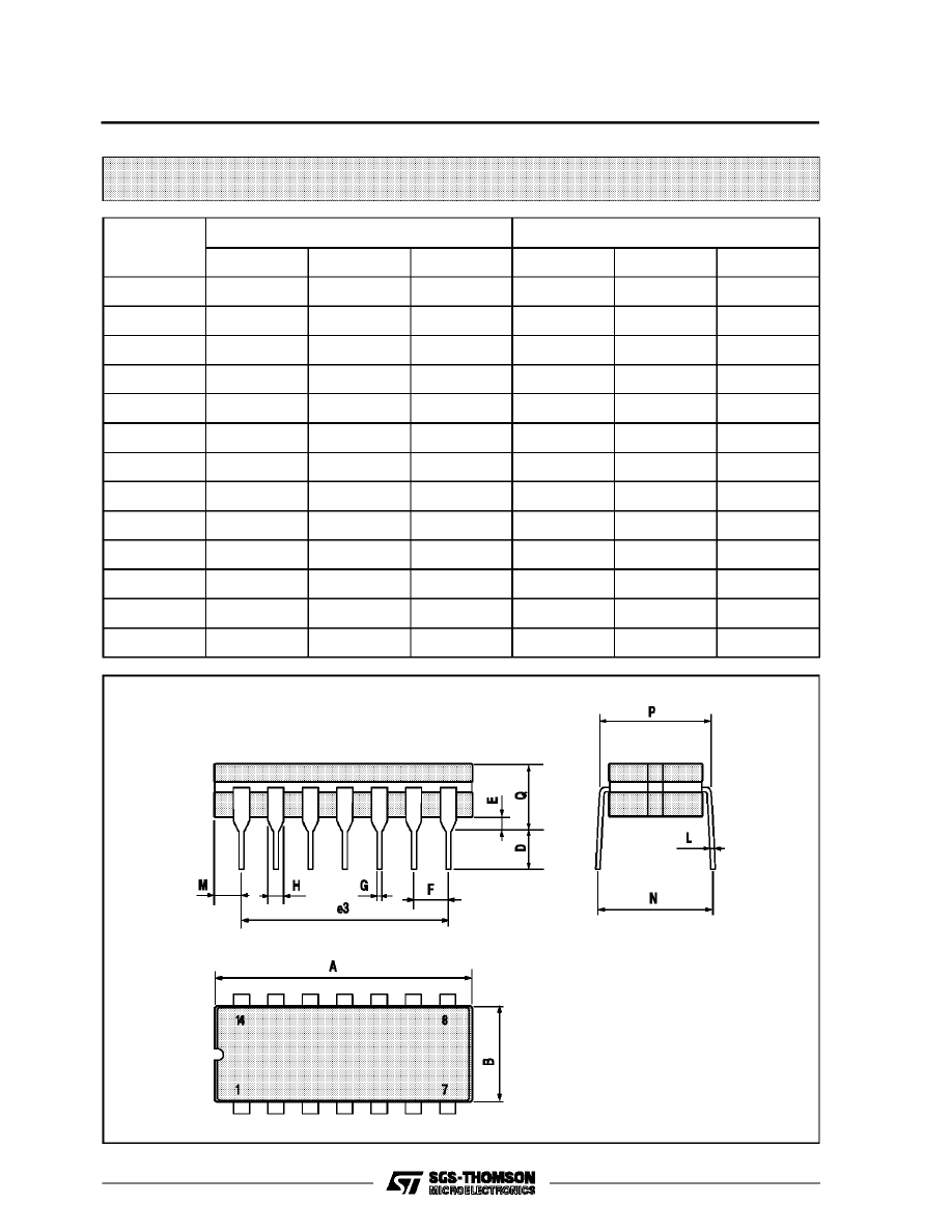
Ceramic DIP14/1 MECHANICAL DATA
DIM.
mm
inch
MIN.
TYP.
MAX.
MIN.
TYP.
MAX.
A
20
0.787
B
7.0
0.276
D
3.3
0.130
E
0.38
0.015
e3
15.24
0.600
F
2.29
2.79
0.090
0.110
G
0.4
0.55
0.016
0.022
H
1.17
1.52
0.046
0.060
L
0.22
0.31
0.009
0.012
M
1.52
2.54
0.060
0.100
N
10.3
0.406
P
7.8
8.05
0.307
0.317
Q
5.08
0.200
P053C
M54/M74HC05
6/9
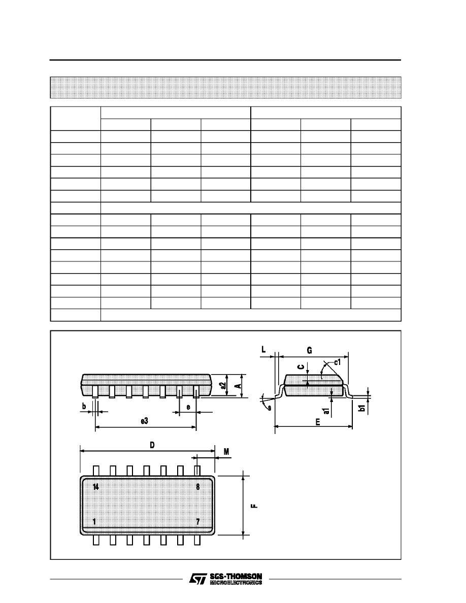
SO14 MECHANICAL DATA
DIM.
mm
inch
MIN.
TYP.
MAX.
MIN.
TYP.
MAX.
A
1.75
0.068
a1
0.1
0.2
0.003
0.007
a2
1.65
0.064
b
0.35
0.46
0.013
0.018
b1
0.19
0.25
0.007
0.010
C
0.5
0.019
c1
45
°
(typ.)
D
8.55
8.75
0.336
0.344
E
5.8
6.2
0.228
0.244
e
1.27
0.050
e3
7.62
0.300
F
3.8
4.0
0.149
0.157
G
4.6
5.3
0.181
0.208
L
0.5
1.27
0.019
0.050
M
0.68
0.026
S
8
°
(max.)
P013G
M54/M74HC05
7/9
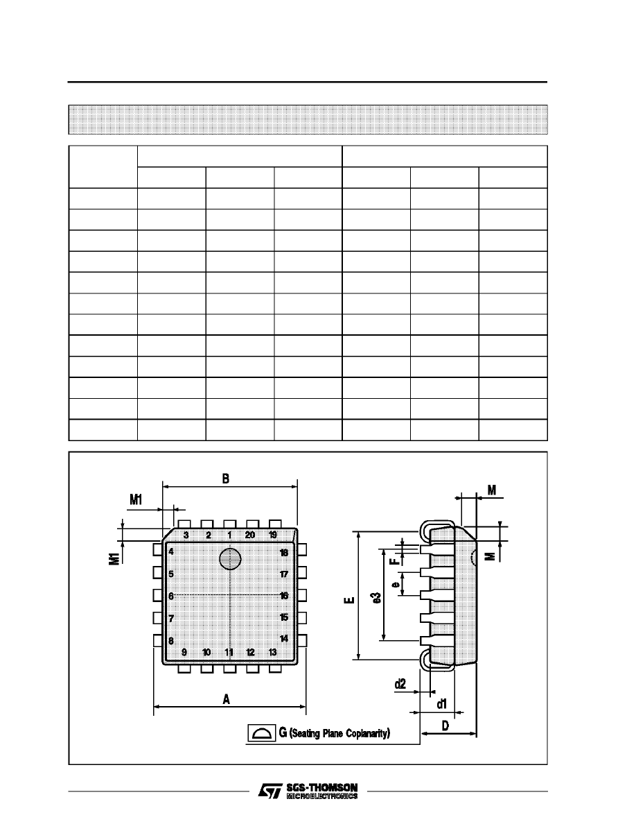
PLCC20 MECHANICAL DATA
DIM.
mm
inch
MIN.
TYP.
MAX.
MIN.
TYP.
MAX.
A
9.78
10.03
0.385
0.395
B
8.89
9.04
0.350
0.356
D
4.2
4.57
0.165
0.180
d1
2.54
0.100
d2
0.56
0.022
E
7.37
8.38
0.290
0.330
e
1.27
0.050
e3
5.08
0.200
F
0.38
0.015
G
0.101
0.004
M
1.27
0.050
M1
1.14
0.045
P027A
M54/M74HC05
8/9

Information furnished is believed to be accurate and reliable. However, SGS-THOMSON Microelectronics assumes no responsability for the
consequences of use of such information nor for any infringement of patents or other rights of third parties which may results from its use. No
license is granted by implication or otherwise under any patent or patent rights of SGS-THOMSON Microelectronics. Specifications mentioned
in this publication are subject to change without notice. This publication supersedes and replaces all information previously supplied.
SGS-THOMSON Microelectronics products are not authorized for use as critical components in life support devices or systems without express
written approval of SGS-THOMSON Microelectonics.
1994 SGS-THOMSON Microelectronics - All Rights Reserved
SGS-THOMSON Microelectronics GROUP OF COMPANIES
Australia - Brazil - France - Germany - Hong Kong - Italy - Japan - Korea - Malaysia - Malta - Morocco - The Netherlands -
Singapore - Spain - Sweden - Switzerland - Taiwan - Thailand - United Kingdom - U.S.A
M54/M74HC05
9/9
Wyszukiwarka
Podobne podstrony:
7405
7405
praca-magisterska-7405, Dokumenty(2)
7405
7405
7405
7405
więcej podobnych podstron