
Non-Intrinsic Differential Mode Noise of Switching Power Supplies and Its Implications to Filter Design
1
Chapter 1 Introduction
1.1 Background and Motivation
In the field of power electronics, there is a trend for pushing up switching frequencies
of switched-mode power supplies to reduce volume and weight. This trend inevitably
contributes to an increasing level of electromagnetic interference (EMI) emissions. It
leads to a general electromagnetic compatibility (EMC) degradation for electronic
devices. As a consequence, EMC legislation is getting more stringent in many countries.
Electromagnetic Interference (EMI) problems in switching power supplies have been
traditionally treated with cut-and-try approaches. In recent years, advancement has been
made to better understand the problems and minimize the cut-and-try portion of the
design process. However, there are still phenomena difficult to explain in many practical
design situations. Very often, the problems may be solved by luck but many puzzles
remain unsolved.
Conventionally, the total conducted EMI noise is caused by two mechanisms, the
differential-mode (DM) and the common-mode (CM) noise. Generally speaking, the DM
noise is related to switching current and the CM noise is related to capacitive coupling of
switching voltage into line impedance stabilizing network (LISN), which is used in
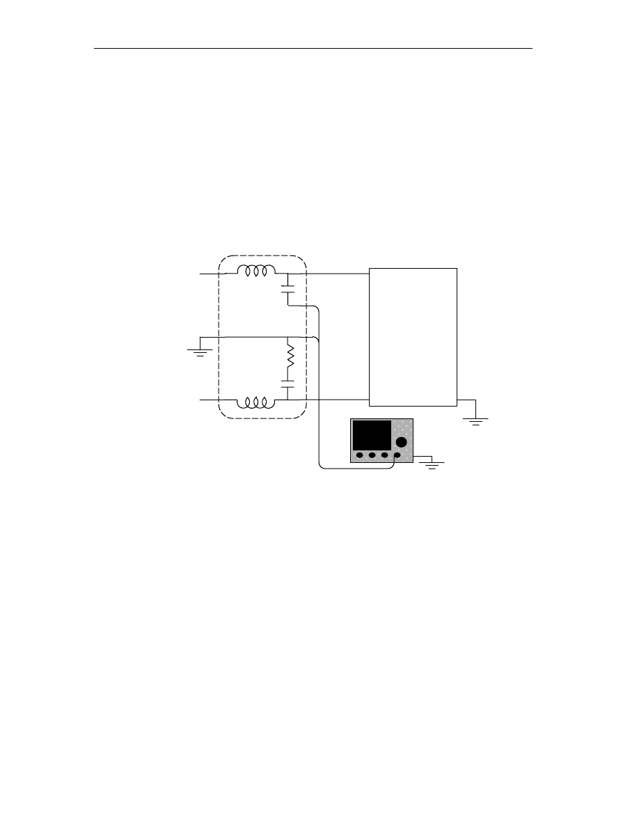
standard conducted EMI measurement. Fig.1-1 shows the typical setup for conducted
EMI measurement. The LISN contains inductors, capacitors and 50
Ω
resistors. For 60 Hz
line frequency, the inductors are basically shorted, the capacitors are open, and the power
Non-Intrinsic Differential Mode Noise of Switching Power Supplies and Its Implications to Filter Design
2
passes through to supply the equipment under test (EUT). For EMI noise frequency, the
inductors are essentially open, the capacitors are shorted and the noise sees 50
Ω
resistors.
The noise voltage measured across the 50
Ω
input impedance of a spectrum analyzer is
defined as the conducted EMI emission.
Fig. 1-1 Conducted EMI Measurement Setup
EMI filters are normally divided into two sections, one deals with DM noise and the
other deals with CM noise. Usually, both DM and CM noises need to be suppressed to
pass EMI limits.
One of the phenomena uncovered recently is the Non-Intrinsic Differential-Mode
(NIDM) noise in an off-line switching power supplies [1]. This phenomenon was
Equipment
Under
Test
LISN
L
G
N
Spectrum Analyzer
50 Ohm

Non-Intrinsic Differential Mode Noise of Switching Power Supplies and Its Implications to Filter Design
3
accidentally discovered in the process to explain certain EMI filter action but was never
thoroughly investigated. The focus of the thesis is to further study the phenomenon and to
investigate the implications of this phenomenon to practical EMI filter design issues.
1.2 Outline of Thesis
In the thesis, the NIDM phenomenon will be briefly reviewed in chapter 2, which is
crucial to the understanding of the remaining chapters. Two diagnostic tools were used to
investigate this phenomenon. One is the DM/CM noise separator [2] and the other is the
zero-span mode operation of a spectrum analyzer. Both of these will be reviewed in this
chapter.
In chapter 3, the results of the investigation will be presented. The results will be
presented using practical examples, which tie the phenomenon to filter design issues. In
some examples, explanations are given to dispel the puzzles commonly encountered in
the practice.
In view of the NIDM phenomenon, the design procedure for EMI filter needs
modification. This is the topic of Chapter 4. A practical filter design procedure presented
in [3] will be modified to incorporate the NIDM phenomenon. Only first-order and
second-order filter topologies are included in the discussion.
Chapter 5 concludes the thesis with recommendations for future research possibilities.

Non-Intrinsic Differential Mode Noise of Switching Power Supplies and Its Implications to Filter Design
4
Chapter 2 Non-Intrinsic Differential Mode Noise
In this chapter, the basic mechanism of Non-Intrinsic Differential Mode conducted
EMI emission will be reviewed. A commonly used switching power supply circuit will be
used as an example to illustrate the phenomenon. The review of this phenomenon is
crucial to the understanding of the remaining chapters of the thesis. Before the NIDM
review, a conventional theory of conducted EMI coupling mechanism will also be briefly
reviewed.
2.1 Review of Conventional Conducted EMI Theory
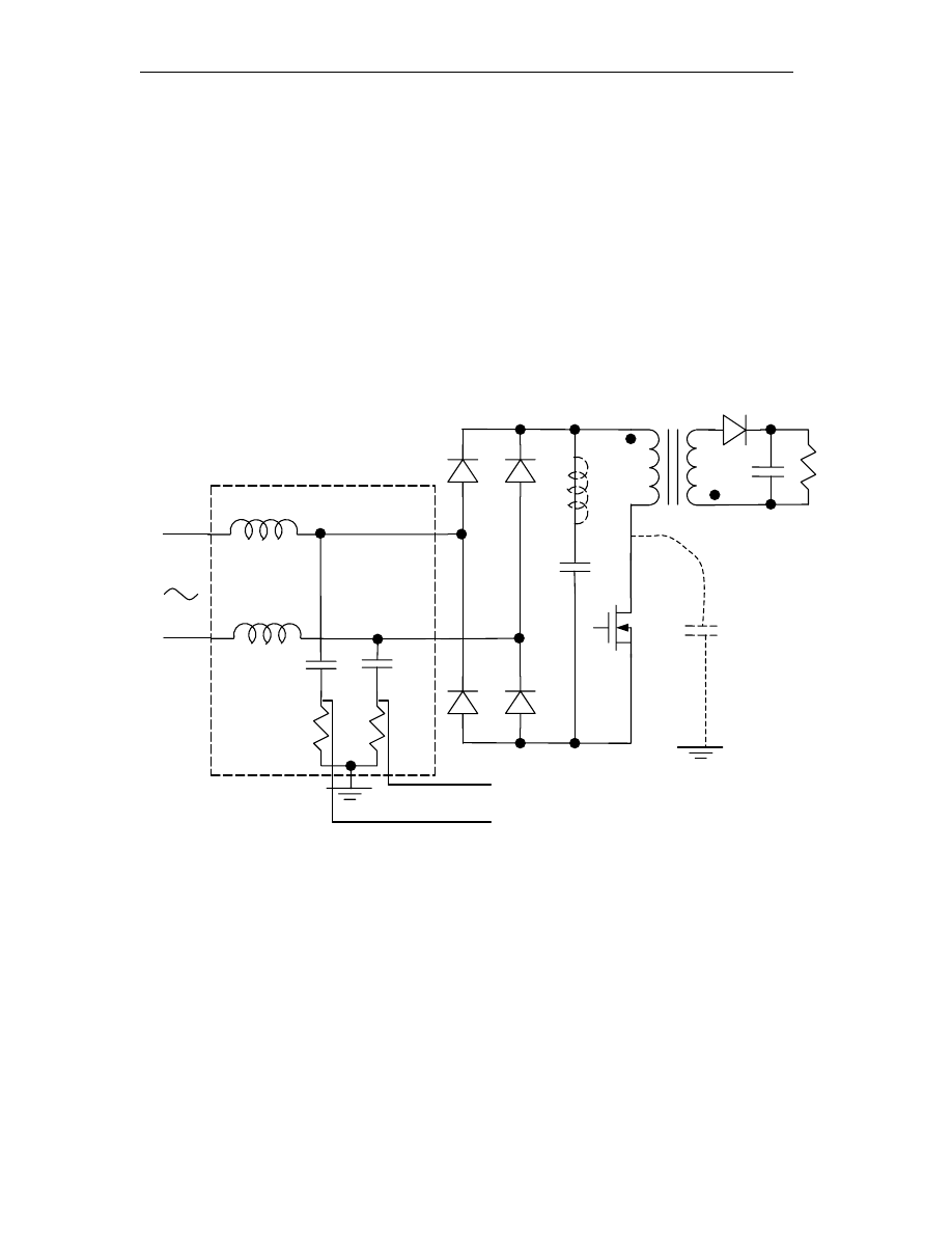
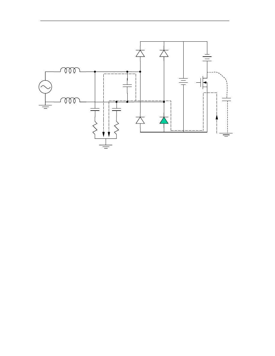
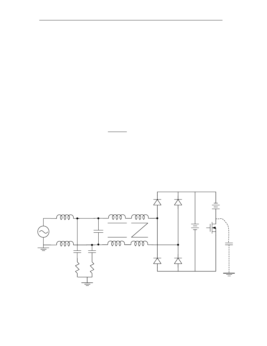
Fig.2-1 shows a typical offline switching power supply with conducted EMI
measurement setup. In the diagram, a Line Impedance Stabilizing Network (LISN) is
used for the measurement of conducted EMI emissions. LISN is used as a standard for
repeatable EMI measurement. The standard components inside the LISN are such that for
60 Hz AC power, the inductance (50
µ
H) presents very small impedance and capacitor
(0.1
µ
F) is essentially open circuit. Therefore, the 60Hz power flows unperturbed. For
high frequency noise, however, the inductance looks like open circuit and the capacitor is
basically short circuit.
Because of the switching nature of the circuit, high frequency noise current could be
coupled into the 50
Ω
resistors. The voltage across the 50
Ω
resistors is counted as the
Non-Intrinsic Differential Mode Noise of Switching Power Supplies and Its Implications to Filter Design
5
conducted EMI emission. Both the line side (Vx) and the neutral side (Vy) EMI must
pass specs. The noise is classified into two modes: Common-Mode (CM), which is
average of Vx and Vy ((Vx+Vy)/2), and Differential-Mode (DM) which is the difference
between Vx and Vy (Vx-Vy).
Fig.2-1 A Typical Switching Power Supply Circuit
Cp
A
B
50
µ
H
50
µ
H
0.1
µ
F
0.1
µ
F
50
Ω
50
Ω
D1
D2
D4
D3
C
B
E
C
D
LISN
60Hz
N
L
Lp
Vx
Vy
To spectrum analyzer
Non-Intrinsic Differential Mode Noise of Switching Power Supplies and Its Implications to Filter Design
6
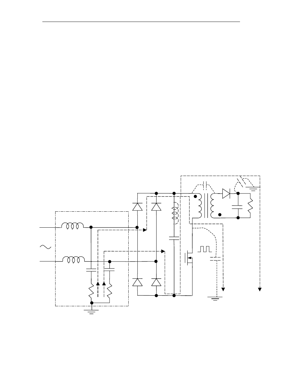
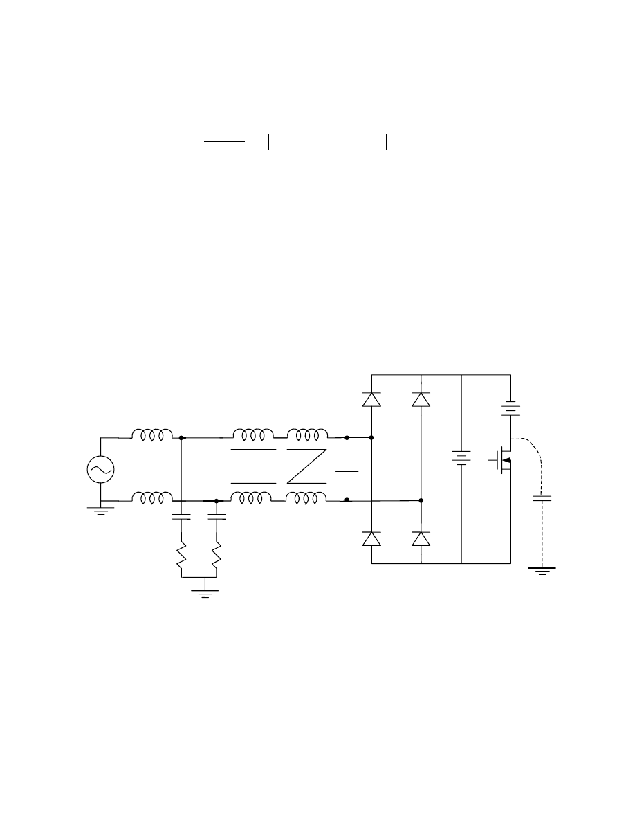
2.1.1 CM Noise
The CM noise is coupled through Cp, the parasitic capacitance between the drain of
the MOSFET (which is usually tied to the heat sink) and the metal enclosure (which is
tied to the ground for safety reason) of the power supply. Since the MOSFET is operated
as a switch, the drain voltage swings from low to high in half of the switching cycle and
from high to low in the second half of the switching cycle. This voltage swing in turn
causes the charging and discharging of the parasitic capacitance. The charging and
discharging current will return through the ground path and show up on the LISN
resistors as CM noise. The CM noise path is illustrated with dash line in Fig.2-2. Notice
that the noise current flows through the two 50
Ω
resistors in parallel.
Fig.2-2 Noise Path of CM Noise
Cp
A
B
50
µ
H
50
µ
H
0.1
µ
F
0.1
µ
F
50
Ω
50
Ω
D1
D2
D4
D3
C
B
E
C
D
LISN
60Hz
N
L
Lp

Non-Intrinsic Differential Mode Noise of Switching Power Supplies and Its Implications to Filter Design
7
Fig.2-2 shows the current path when Cp is charged. When Cp is discharged, the
current direction reverses but both currents flow in phase. Therefore, it is called common-
mode noise. In general, CM noise is voltage dependent and depends on parasitic
capacitance. Besides the parasitic capacitance of MOSFET drain, there are other parasitic
capacitors (such as the parasitic capacitance between the transformer primary and
secondary windings and the parasitic capacitance of the secondary rectifier diode),
through which the CM noise current can couple.
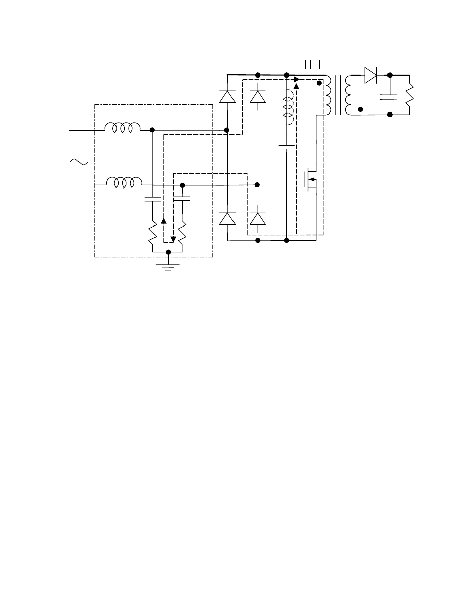
2.1.2 DM Noise
Another mode of conducted EMI noise coupling through the 50
Ω
resistors is shown in
Fig.2-3. Because of the switching nature of the MOSFET current, part of the switch
current flows through the bulk capacitor C
B
and part through the 50
Ω
resistors as
indicated by the dash line. Since C
B
is not perfect due to the existence of parasitic
inductance Lp, there is certain amount of noise current flowing through the 50
Ω
resistors.
Notice that the current flows through the resistors in series. In general, the DM noise
current is load dependent and is affected by Lp and C
B
. This is what the conventional
theory says. But in further exploration, we can find there is insufficiency in the theory to
explain certain noise phenomenon. A new noise coupling mechanism call Non-Intrinsic
Differential Mode (NIDM) noise was uncovered [1] recently. This phenomenon will be
discussed in Section 2.3.
Non-Intrinsic Differential Mode Noise of Switching Power Supplies and Its Implications to Filter Design
8
Fig.2-3 Noise Path of DM Noise
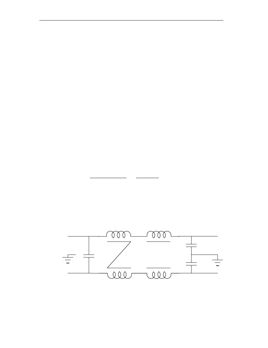
2.2 Diagnosis Tools for Investigating NIDM
Two important measuring tools are utilized in the present research on conducted EMI
emission. The functions and operation principles are reviewed. Without these two tools, it
is not possible to investigate the NIDM noise phenomenon, which is the main focus of
the present thesis.
A
B
50
µ
H
50
µ
H
0.1
µ
F
0.1
µ
F
50
Ω
50
Ω
D1
D2
D4
D3
C
B
E
C
D
LISN
60Hz
N
L
Lp

Non-Intrinsic Differential Mode Noise of Switching Power Supplies and Its Implications to Filter Design
9
2.2.1 Noise Separator
The noise spectrum measured directly from LISN resistors is total noise. To
investigate CM and DM respectively, a noise separator [2] was used for separating CM
noise from DM noise.
The concept of the noise separator is very simple. Fig.2-4 shows the diagrams
depicting this concept. Two signals (A and B) derived from the LISN consist of both CM
and DM noises. However, one of the signals is the vector sum of the two modes, and the
other signal is the vector difference of the two modes. It is assumed that the CM current
is often evenly divided between the two input terminals.
A device called power combiner is used to separate these two kinds of noises. There
are two types of power combiners in the noise separator, 0
°
power combiner and 180
°
power combiner. The output of a 0
°
power combiner is the sum of the two input signals,
and the output of a 180
°
power combiner is the difference of the two input signals. In the
noise separator, the 0
°
power combiner cancels out the DM component and lets through
the CM component through. The 180
°
power combiner cancels out the CM component
and lets through the DM component.
Power combiners are used mainly for the radio frequency performance because of the
EMI frequency requirement. The insertion of the noise separator does not perturb the
measurement setup because the impedance seen from point A to ground (or from point B
to ground) is still 50
Ω
.
Non-Intrinsic Differential Mode Noise of Switching Power Supplies and Its Implications to Filter Design
10
(a) DM Rejection
(b) CM Rejection
Fig.2-4 Principles of Noise Separator
A
0° Power
Combiner
Spectrum
Analyzer
50
CM
B
CM+DM
CM-DM
L
N
To EUT
To EUT
LISN
A
180° Power
Combiner
Spectrum
Analyzer
50
DM
B
CM+DM
CM-DM
L
N
To EUT
To EUT
LISN

Non-Intrinsic Differential Mode Noise of Switching Power Supplies and Its Implications to Filter Design
11
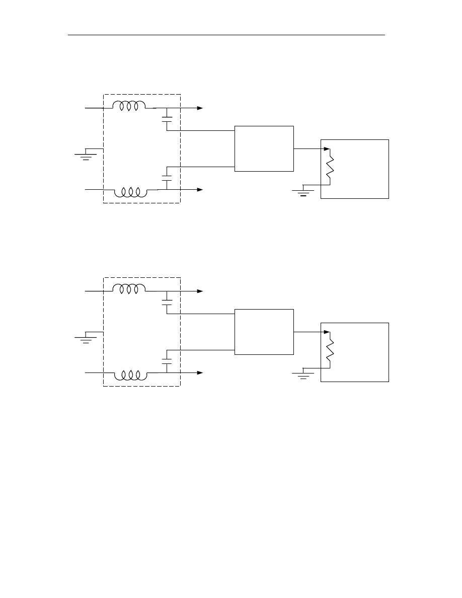
2.2.2 Zero-Span Mode of Spectrum Analyzer
Zero-span mode is a special operation mode of a spectrum analyzer. In this mode, the
spectrum analyzer scans at a fixed frequency point (center frequency) and displays the
amplitude in term of time. In zero-span mode, the spectrum analyzer behaves just like an
oscilloscope; i.e. the horizontal axis represents time instead of frequency. The major
difference between a spectrum analyzer in zero-span mode and an oscilloscope is that the
spectrum analyzer usually detects and displays only the peak of the time domain signal at
the output of RBW filter, while the oscilloscope displays instantaneous values.
Zero-span mode is sometimes a more convenient way to look at amplitude-modulated
signals when the modulating signal is of very low frequency.
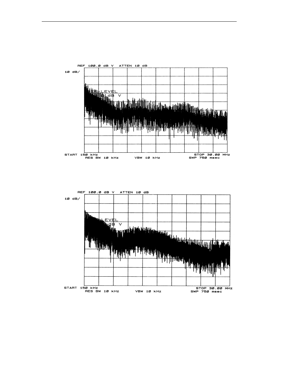
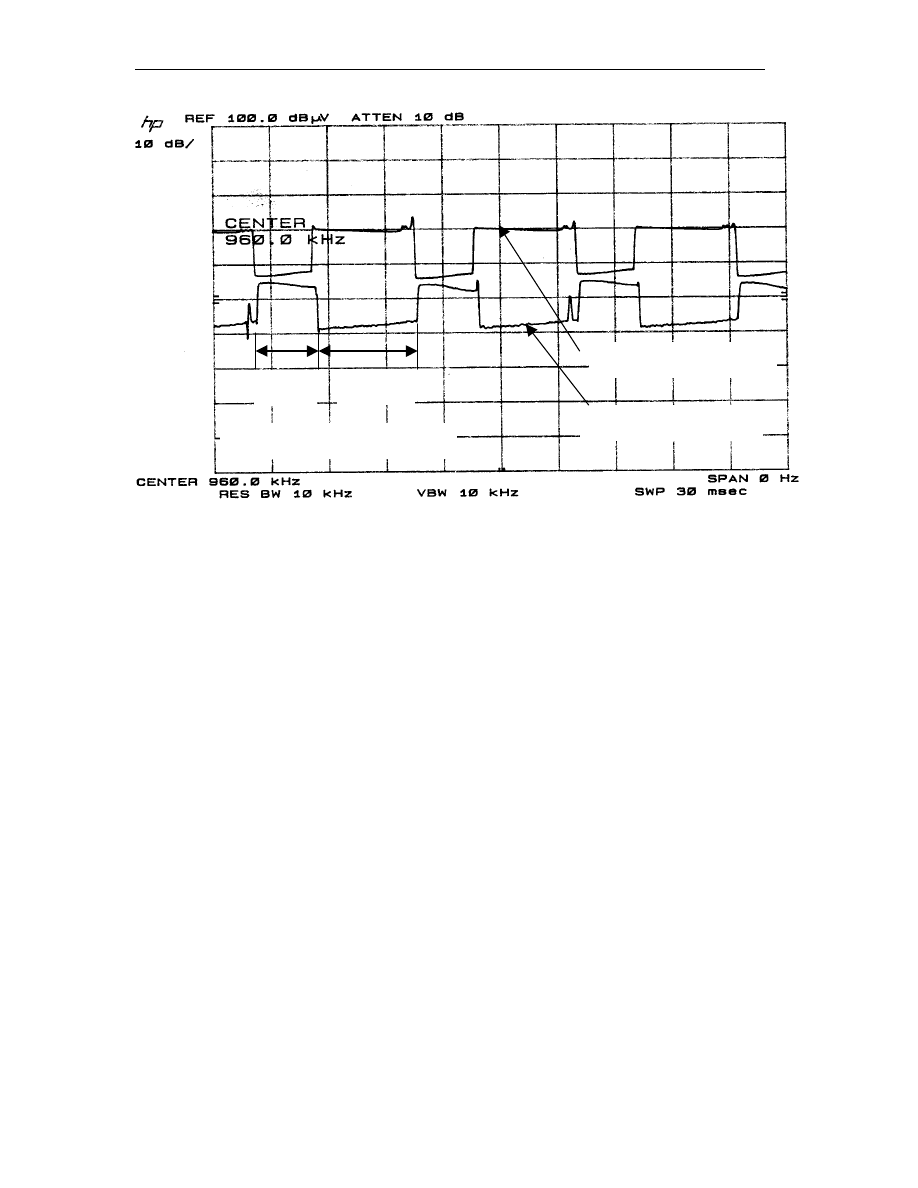
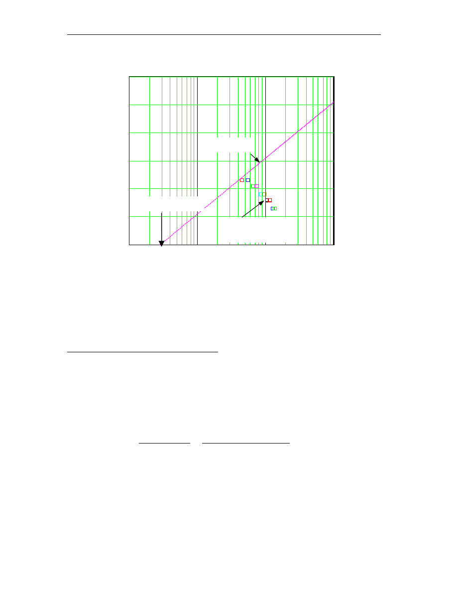
Fig. 2-5 illustrates two pictures. Fig.2-5 (a) shows the typical EMI noise spectrum.
The horizontal axis is the frequency. The emission level, in some cases, may fluctuate
with time. In such cases, obviously, the peak of the emission has to pass the specs. If one
wishes to investigate the fluctuating behavior of the emission at a particular frequency,
then the Zero-Span mode operation of the spectrum analyzer should be used. Fig.2-5 (b)
shows the emission at 960kHz in zero-span mode. Notice that the horizontal axis now is
the time. In other words, the fluctuating behavior of this frequency is displayed in that
picture. This mode of operation will be used frequently in the remaining chapters.
Non-Intrinsic Differential Mode Noise of Switching Power Supplies and Its Implications to Filter Design
12
(a) Noise Displayed in Normal Operation Mode
(b) Noise Displayed in Zero-Span Mode
Fig.2-5 Spectrum Analyzer Display of EMI Noise
Time (ms)
30
0
Frequency (MHz)
30
0.15
Non-Intrinsic Differential Mode Noise of Switching Power Supplies and Its Implications to Filter Design
13
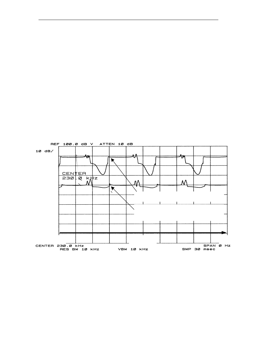
2.3 Non-Intrinsic Differential Mode Noise
2.3.1 Description of NIDM Phenomenon
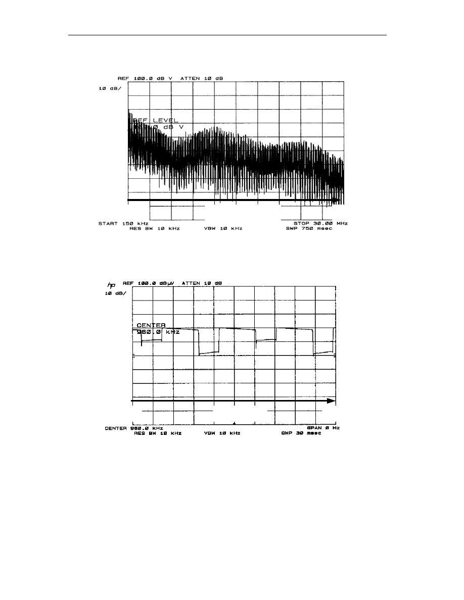
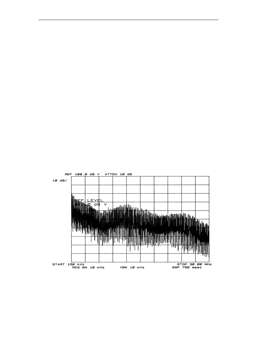
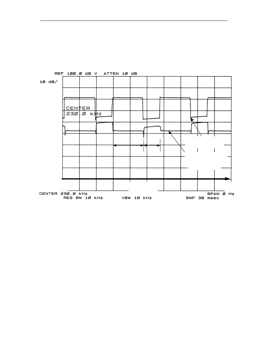
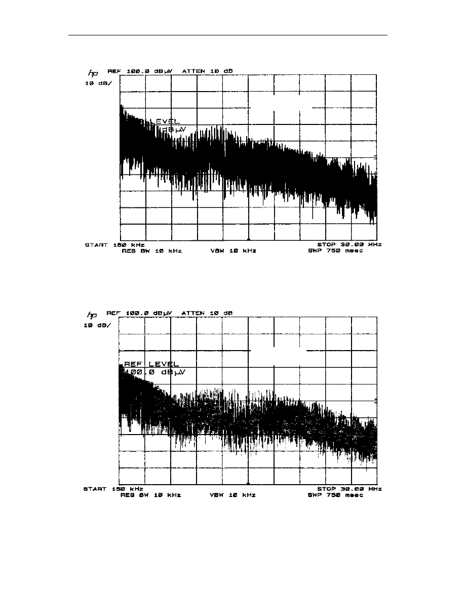
Fig.2-6 shows the standard EMI emission measurement results obtained using
spectrum analyzer. In the oscillogram, the amplitude of the spectrum fluctuate with time
because of input rectifier diodes “on” and “off”. One would ask: “Is the EMI emission
larger when the rectifier diodes are ‘on’ or when they are ‘off’?” From the conventional
conducted EMI theory given in Section 2.2, one would naturally assume that EMI is
larger when diodes are “on”. Because when diodes are “on”, the noisy switch current
flows through the 50
Ω
resistors. However, the experimental results shown in Fig.2-7
indicate otherwise as will be explained below.
Fig.2-6 DM Emission Measurement Result
Non-Intrinsic Differential Mode Noise of Switching Power Supplies and Its Implications to Filter Design
14
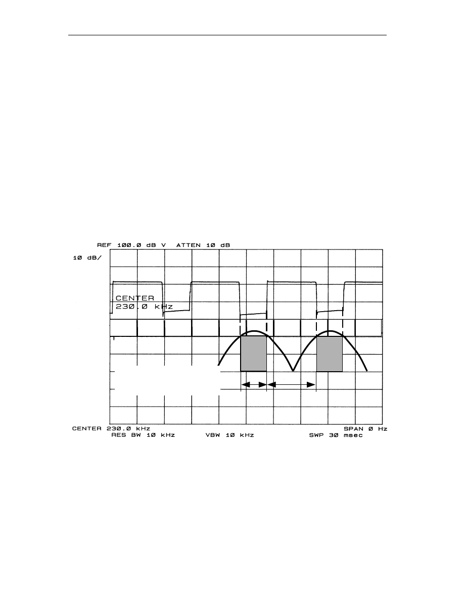
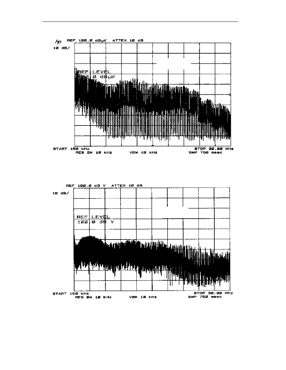
A noise separator can be used to measure CM and DM emissions respectively. The
measured DM emission often fluctuates with time because the conduction states of input
rectifier diodes (D1 to D4) change between “on” and “off” during the 120 Hz cycle. The
amplitude fluctuation of DM noise at a particular frequency can be displayed on a
spectrum analyzer using zero-span mode as explained in Section 2.2. Fig.2-7 shows the
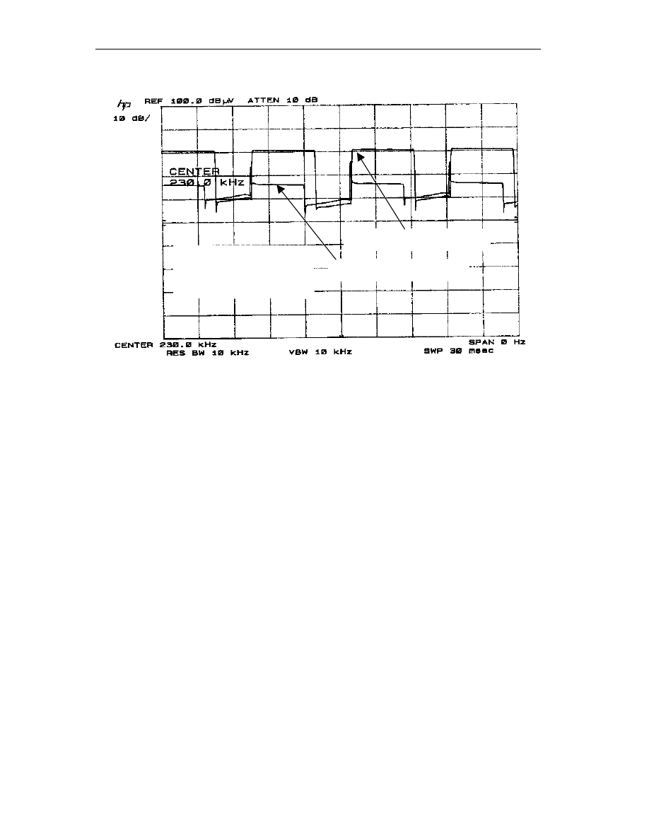
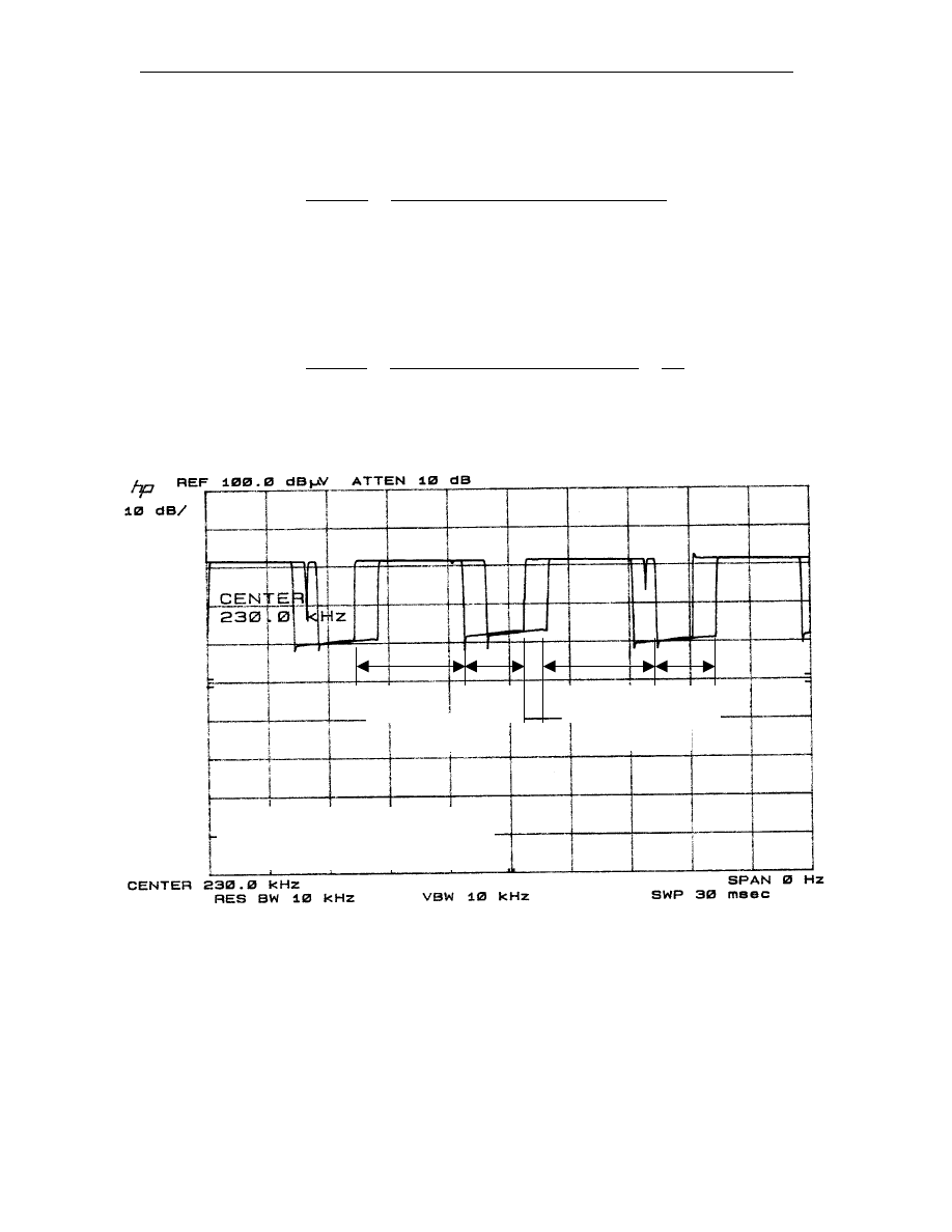
DM noise of a typical off-line switching power supply observed in zero-span mode. The
center frequency is set at 230 kHz, which is the harmonic of the power supply switching
frequency.
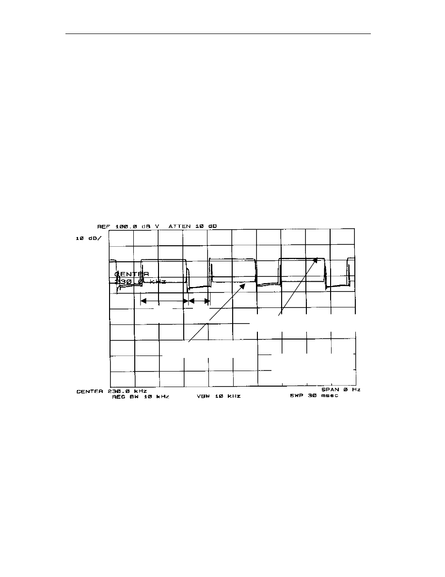
Fig.2-7 DM Noise Displayed in Zero-Span Mode
A
B
A: diodes on (IDM)
B: diodes off (NIDM)

Non-Intrinsic Differential Mode Noise of Switching Power Supplies and Its Implications to Filter Design
15
Two time intervals are marked in the figure. Interval A corresponds to the “on” state,
and interval B to the “off” state of input rectifier diodes. The two intervals together form
a complete 120 Hz cycle, which is two times the input line frequency. It can be seen that
the noise is higher when the rectifier diodes are cut off than when two diodes are
conducting. This phenomenon cannot be explained by conventional theory of DM noise
generation. Investigation of that phenomenon led to the discovery of a new DM noise-
coupling mode. DM noise coupled through LISN with this phenomenon is called Non-
Intrinsic Differential Mode (NIDM) noise. To distinguish, we call the noise coupled
through when rectifier diodes are “on” Intrinsic Differential Mode (IDM) noise. The
conventional EMI theory can only explain the generation of IDM.
2.3.2 NIDM Noise Generation Mechanism
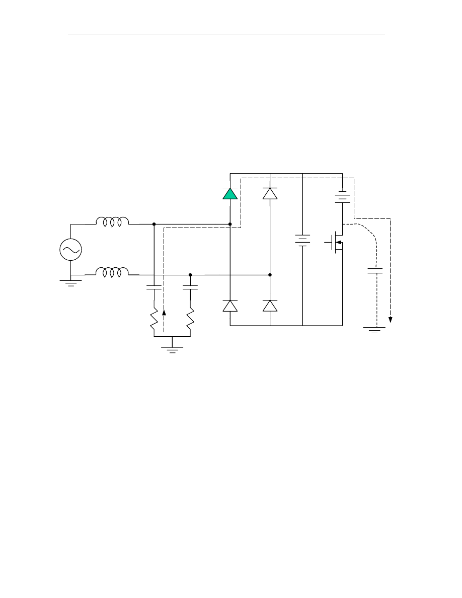
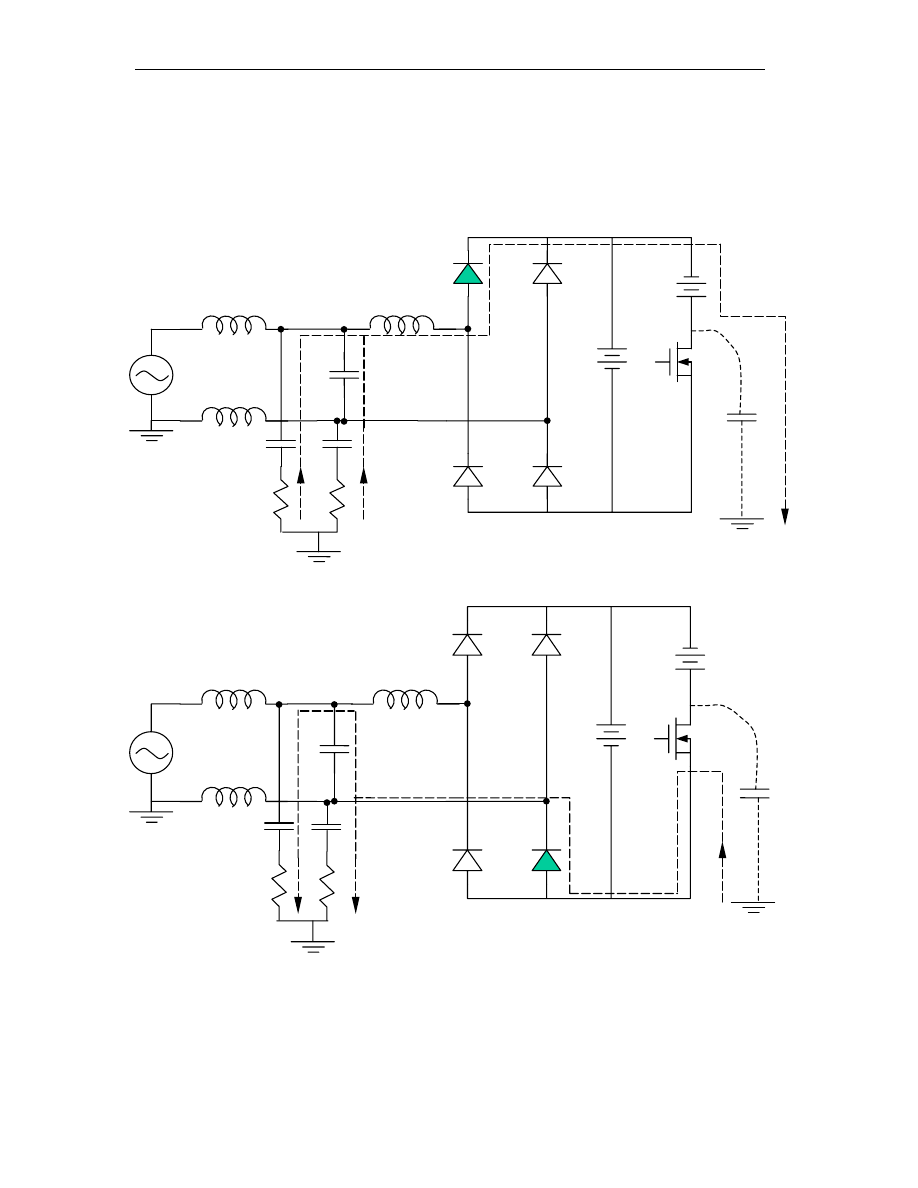
2.3.2.1. Rectifier Diodes On
First, we consider the situation when two of the rectifier diodes are conducting.
Fig.2-8 illustrates the noise current path when the switch is being turned off. When the
switch is off, the voltage potential of point E is raised from zero potential to V2+V3. The
parasitic capacitance Cp is being charged by V2 and V3. There exist two noise current
paths. One path is from the earth ground, passing by R1, C1, point A, D1, point C, to
point E. The other one is from the earth ground, passing by R2, C2, point B, D3, point D,
point C, to point E. Because both D1 and D3 are conducting, the potential of point A is
equal to that of point C, while the potential of point B is also equal to that of point D.
Therefore, the impedance of two noise paths are almost the same. The noise current can
be distributed evenly between the two noise paths.
Non-Intrinsic Differential Mode Noise of Switching Power Supplies and Its Implications to Filter Design
16
Fig.2-8 Rectifier Diodes On; Switch being Turned Off
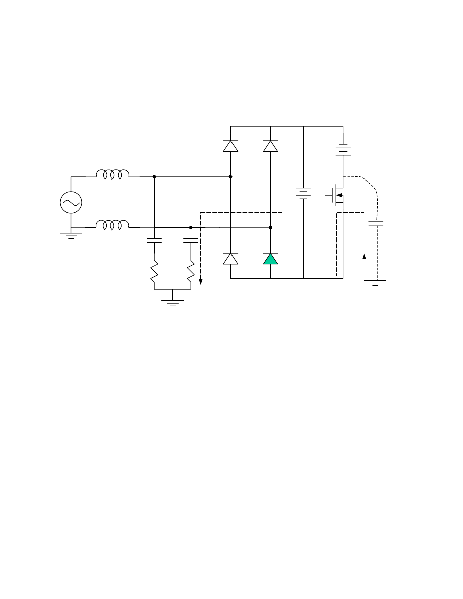
Fig.2-9 shows a similar situation when the switch is being turned on and the parasitic
capacitance is being discharged. There are also two noise paths. One is from point E,
passing by point D, point C, D1, point A, C1, R1, to the earth ground. The other one is
from point E, passing by point D, D3, point B, C2, R2, to the earth ground. Because
VA=VC and VB=VD, the impedance of two noise paths are almost the same and the
noise current can be distributed evenly between the two paths.
Cp
A
B
V2
V3
D1
D4
D2
D3
S
D
C
Vs
C1
R1
C2
R2
E
Non-Intrinsic Differential Mode Noise of Switching Power Supplies and Its Implications to Filter Design
17
Fig.2-9 Rectifier Diodes On; Switching being Turned On
Regardless of whether the switch is turned on or off, there exist two paths with almost
identical impedance as long as two diodes are conducting. So the two currents flowing
through the two LISN branches are almost the same. The noise generated in this way is
pure CM noise.
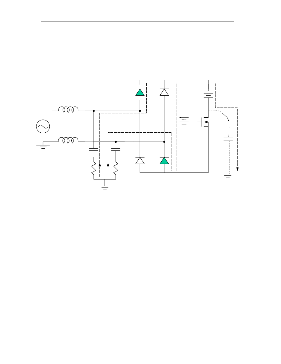
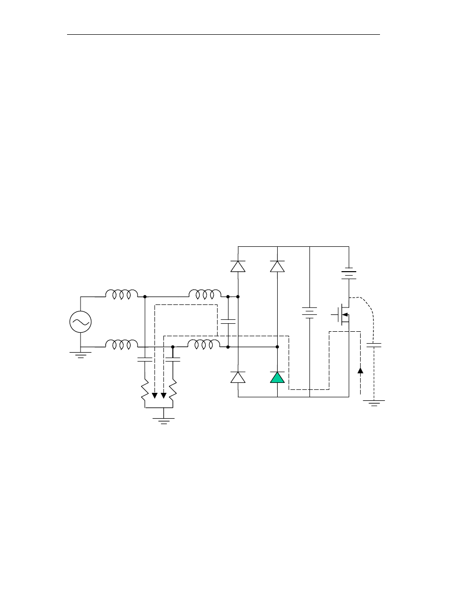
2.3.2.2. Rectifier Diodes Off
For the following discussion, we assume V2 > VAB > 0. In Fig.2-10, the switch was
originally “on”, VE
≈
0V. When the switch is being turned off, V3 finds a path to charge
the parasitic capacitance Cp. The path is from the earth ground, passing by R1, C1, point
Cp
A
B
V2
V3
D1
D4
D2
D3
S
D
C
Vs
C1
R1
C2
R2
E
Non-Intrinsic Differential Mode Noise of Switching Power Supplies and Its Implications to Filter Design
18
A, D1, point C, to point E. So the potential of point E will be raised from zero to VC +
V3, which is equal to VA + V3. Since VC is equal to VA, VD is then equal to VA – V2,
which is less than zero. This means D3 and D4 are reversed biased. Since only one diode
D1 conducts, there is noise current flowing through only one LISN branch, resulting in
differential mode noise, which is NIDM.
Fig.2-10 Rectifier Diodes Off; Switch being Turned Off
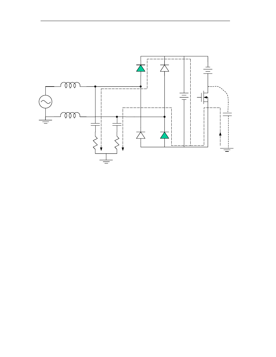
A similar situation is shown in Fig.2-11, the switch was originally in “off” position,
VE = VA + V3 > 0. When the switch is being turned on, point D is clamped to VA + V3
instantaneously, resulting the discharge of parasitic capacitance Cp. The discharge path is
from point E, passing by point D, D3, point B, C2, R2, to the earth ground. Now the
potential of point D is zero, so VC is equal to V2. Diodes D1 and D2 are being reverse
biased. Again there is only one diode D3 conducting. The noise current will only flow
Cp
A
B
V2
V3
D1
D4
D2
D3
S
D
C
Vs
C1
R1
C2
R2
E
Non-Intrinsic Differential Mode Noise of Switching Power Supplies and Its Implications to Filter Design
19
through one branch of LISN. Because of unbalanced current flow through the two
branches of the LISN, DM noise can be measured.
Fig.2-11 Rectifier Diodes Off; Switch being Turned On
This kind of DM noise is different from conventional DM noise because it is not
related to the input current harmonics. It is related to the charging and discharging of the
parasitic capacitance.
Cp
A
B
V2
V3
D1
D4
D2
D3
S
D
C
Vs
C1
R1
C2
R2
E

Non-Intrinsic Differential Mode Noise of Switching Power Supplies and Its Implications to Filter Design
20
2.4 Basic Characteristics of NIDM
The relationship of NIDM noise with input line voltage and load current will be
discussed in this section.
2.4.1 Dependency of NIDM on Line Voltage
Similar to CM noise, NIDM noise is a voltage-generated phenomenon. The noise
current is mainly determined by dv/dt across the parasitic capacitance. Higher input line
voltage will lead to higher dv/dt. Therefore, the amplitude of NIDM emission is
dependent on the input line voltage, i.e. the higher the input line voltage, the larger the
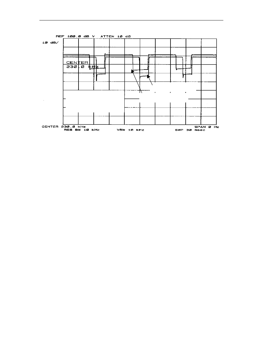
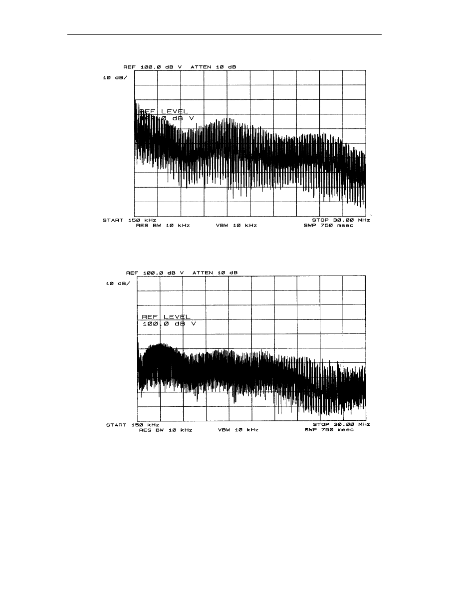
NIDM emission. The above conclusion can be verified by experiments. Fig.2-12 shows
the NIDM noises observed in zero-span mode. The central frequencies and load
conditions are the same for both cases. The only difference is the input line voltage. A
100 W offline flyback switching power supply was used in the measurement. The output
voltage is 5 V DC and the output power is 50 W for both cases. The central frequency is
also the same (230kHz) for both cases. But the input line voltage is 120 V AC for the first
case and is 70 V AC for the second case.
We can see clearly that the input voltage has much more effect on NIDM than on
IDM. Basically IDM is affected by input voltage with minor effect.
Non-Intrinsic Differential Mode Noise of Switching Power Supplies and Its Implications to Filter Design
21
Fig.2-12 NIDM at Different Line Voltages
2.4.2 Dependency of NIDM on Load Current
NIDM is a voltage-generated phenomenon as opposed to a current-generated
phenomenon in IDM noise, so the input line voltage, not the input current, determines the
absolute amplitude of NIDM. Load current (or the input current) can affect NIDM noise
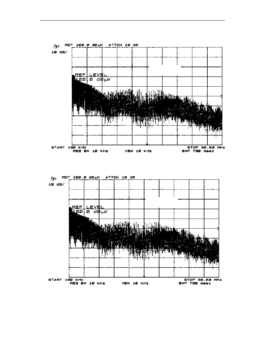
with minor effect. As shown in Fig.2-13, under heavy load condition, the rectifier diode
conduction period is longer than the diode off period. The time interval occupied by IDM
(period a) is longer than that occupied by NIDM (period b). But under light load
condition, the diode conduction period is shorter than the diode off period. In one line
cycle, the interval occupied by NIDM is longer than the other interval occupied by IDM.
As can be seen from the oscillogram, load changes the IDM much more than NIDM
.
120 V Input Line Voltage
70 V Input Line Voltage
Flyback Converter
Output Power: 50 W
Output Voltage: 5 V DC
Non-Intrinsic Differential Mode Noise of Switching Power Supplies and Its Implications to Filter Design
22
Fig.2-13 NIDM at Different Load Currents
Output current: 5A
Output current: 10A
Flyback converter
Input voltage: 110 V AC
Output voltage: 5 V DC

Non-Intrinsic Differential Mode Noise of Switching Power Supplies and Its Implications to Filter Design
23
Chapter 3 Implications of NIDM to EMI Filter Design
In this chapter, the implications of non-intrinsic differential mode (NIDM) noise to
EMI filter design will be discussed. Many puzzles commonly encountered in EMI filter
design can be explained with NIDM phenomenon. Means to attenuate NIDM are also
described in this chapter. An understanding of NIDM has practical implications on filter
design.
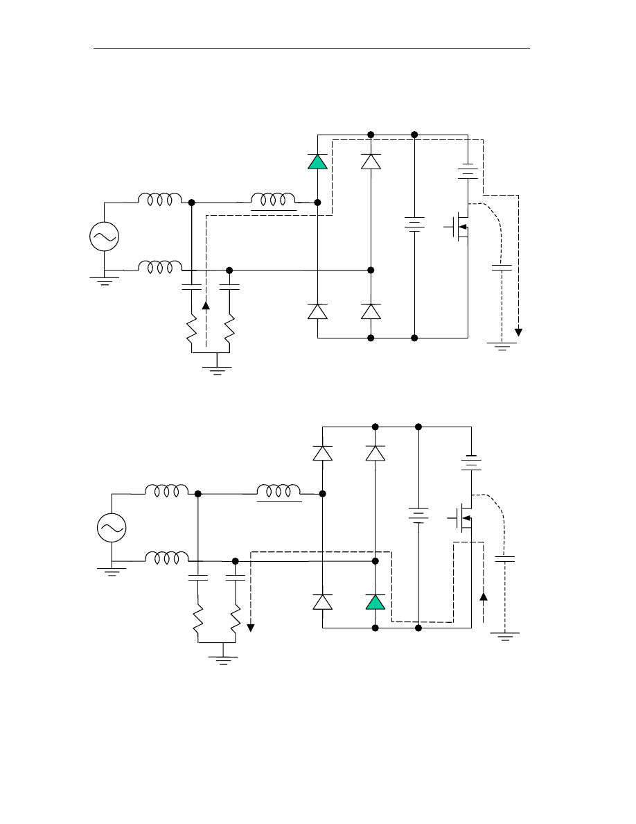
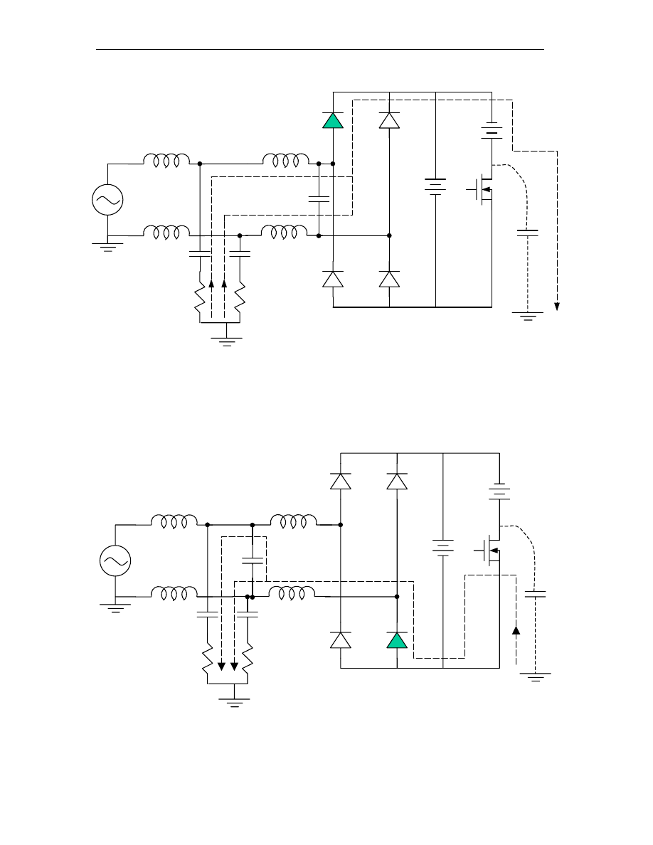
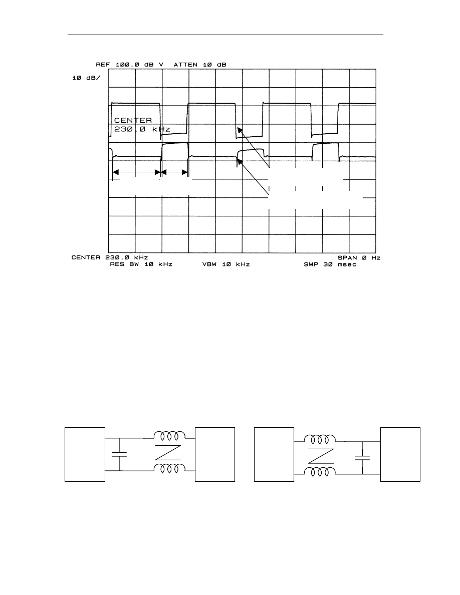
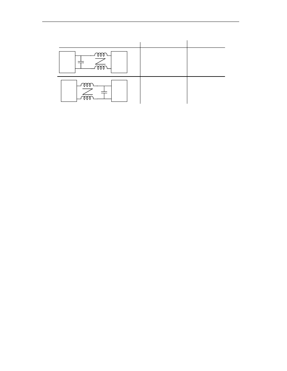
3.1 Asymmetrical DM Choke vs. Symmetrical DM Choke
NIDM noise can be generated during the bridge rectifier “off” period. As we
discussed before, there are two paths for the ground noise current. When the rectifier is
off, the line impedance of one noise path is much higher than the other one. Therefore,
the asymmetry of noise path impedance causes most of the noise current flowing through
the low impedance path and DM noise is generated. Actually, the unbalance of the noise
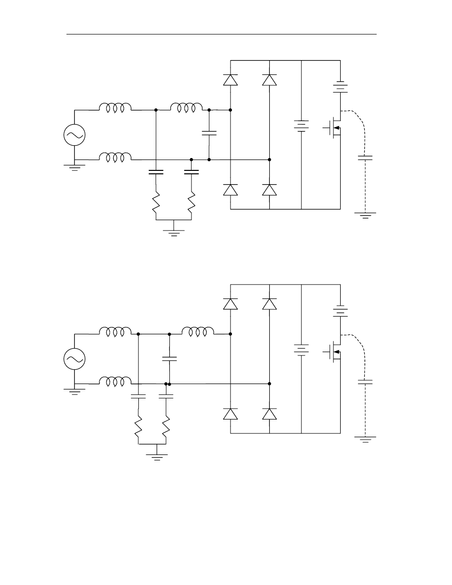
path can also be attributed to asymmetry of filter topology. One example is the DM choke
in a filter. Fig.3-1 shows the power circuit and the two possible filter topologies.
Non-Intrinsic Differential Mode Noise of Switching Power Supplies and Its Implications to Filter Design
24
(a) Asymmetrical DM Choke
(b) Symmetrical DM Choke
Fig.3-1 Test Setup of Asymmetrical Filter
Cp
A
B
V2
V3
D1
D4
D2
D3
S
D
C
Vs
C1
R1
C2
R2
E
LISN
L
DM
1.2mH
Cp
A
B
V2
V3
D1
D4
D2
D3
S
D
C
Vs
C1
R1
C2
R2
E
LISN
L
DM1
600
µ
H
L
DM2
600
µ
H

Non-Intrinsic Differential Mode Noise of Switching Power Supplies and Its Implications to Filter Design
25
The only difference between Fig.3-1 (a) and (b) is that asymmetrical DM choke is used in
Fig.3-1 (a) and symmetrical one used in (b). Notice that the total inductance of the two
chokes in Fig.3-1 (b) is the same as that of the single choke in Fig.3-1 (a). No other filter
elements are used.
3.1.1 Description of Phenomenon
According to conventional conducted EMI emission theory; the DM noise attenuation
of the two filter topologies should be the same because of the same inductance values.
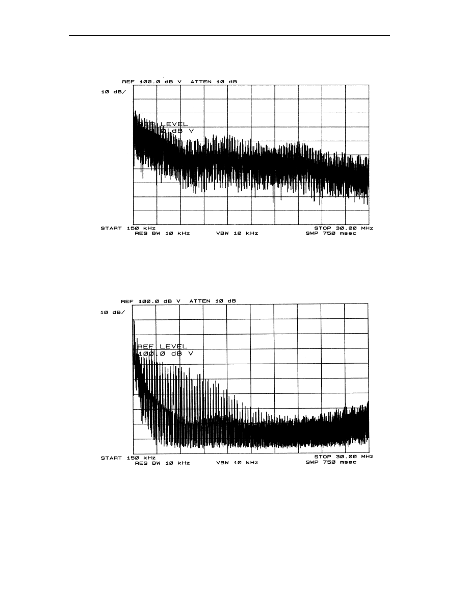
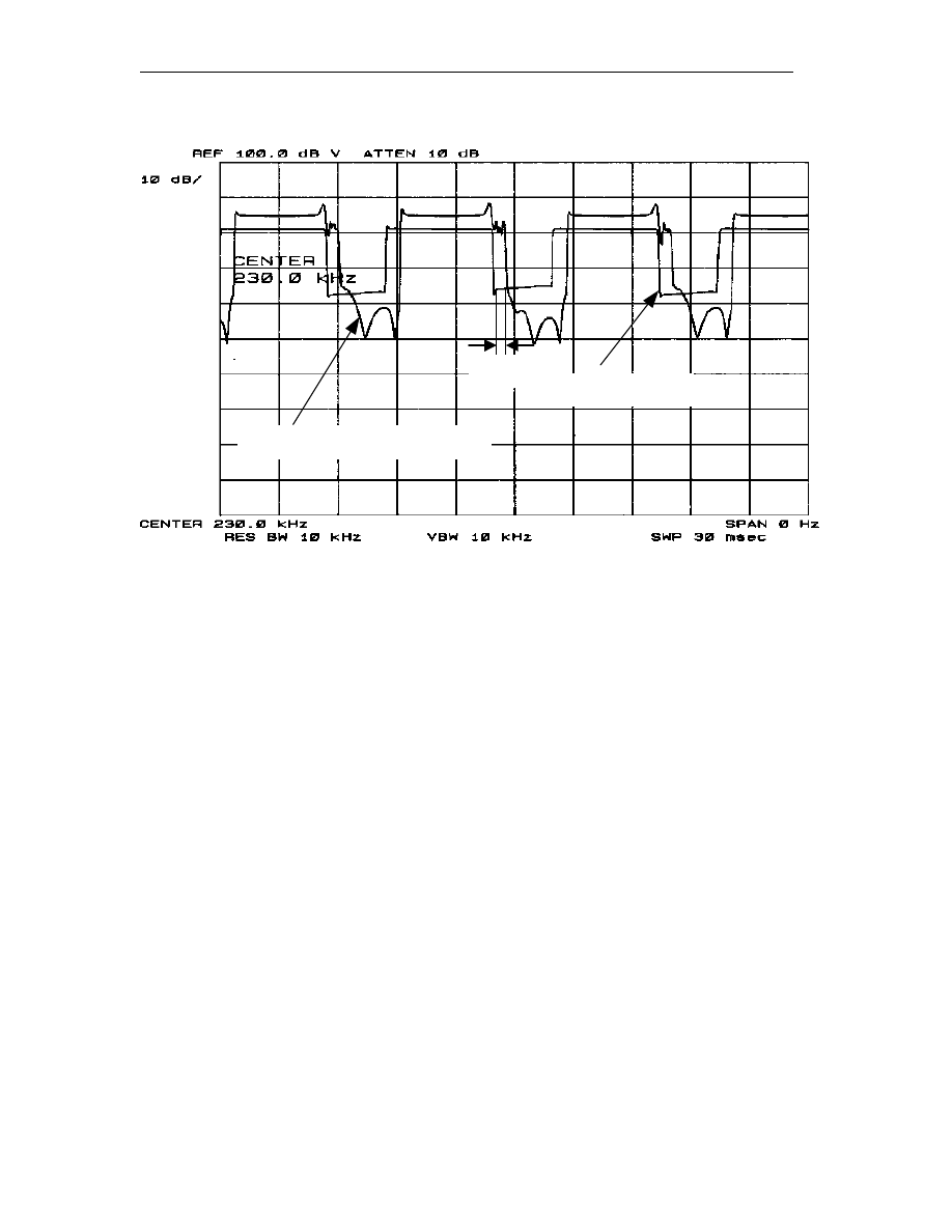
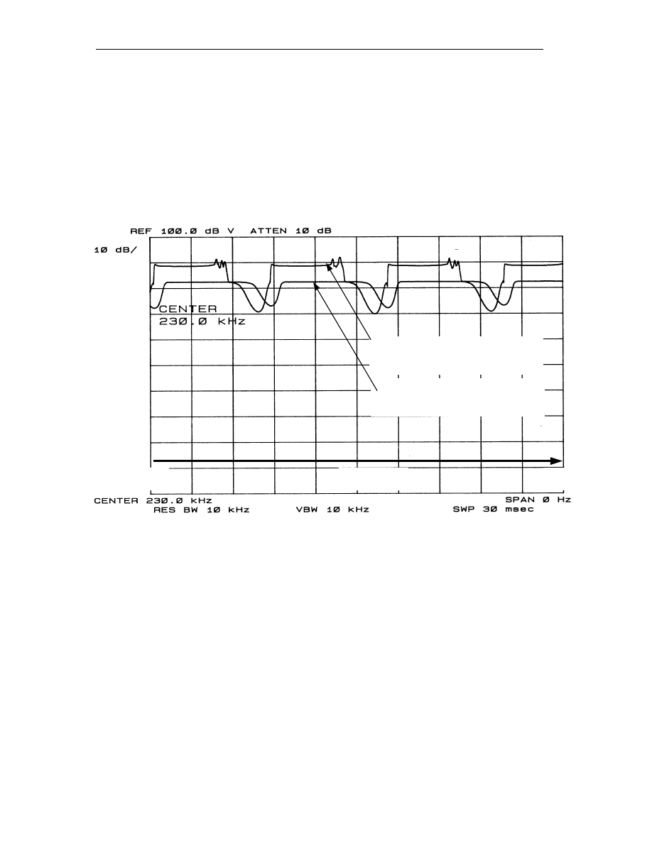
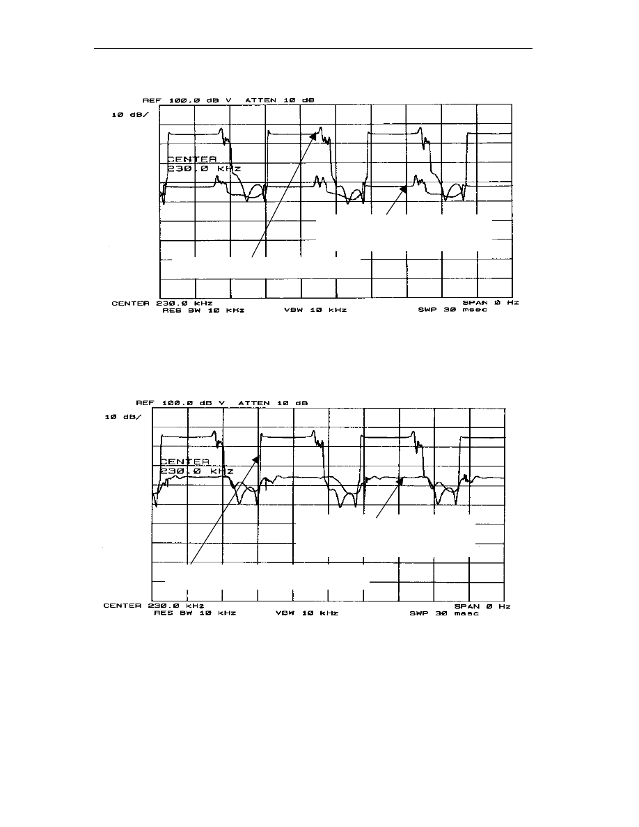
However, the experimental result of Fig.3-2 shows otherwise. Fig.3-2 (a) is the total DM
noise spectrum of the EUT with one 1.2mH DM choke on one side. Fig.3-2 (b) is the DM
noise of the same EUT with two 600
µ
H DM chokes on both sides. It shows clearly that
the noise amplitude in the symmetrical choke case is lower than that of the asymmetrical
case. This phenomenon cannot be explained by the conventional conducted EMI theory.
In the next section, NIDM noise theory discussed in Chapter 2 will be used to analyze
that phenomenon.
Non-Intrinsic Differential Mode Noise of Switching Power Supplies and Its Implications to Filter Design
26
(a) DM Noise with Asymmetrical DM Choke
(b) DM Noise with Symmetrical DM Choke
Fig.3-2 Asymmetrical DM Choke vs. Symmetrical DM Choke
Non-Intrinsic Differential Mode Noise of Switching Power Supplies and Its Implications to Filter Design
27
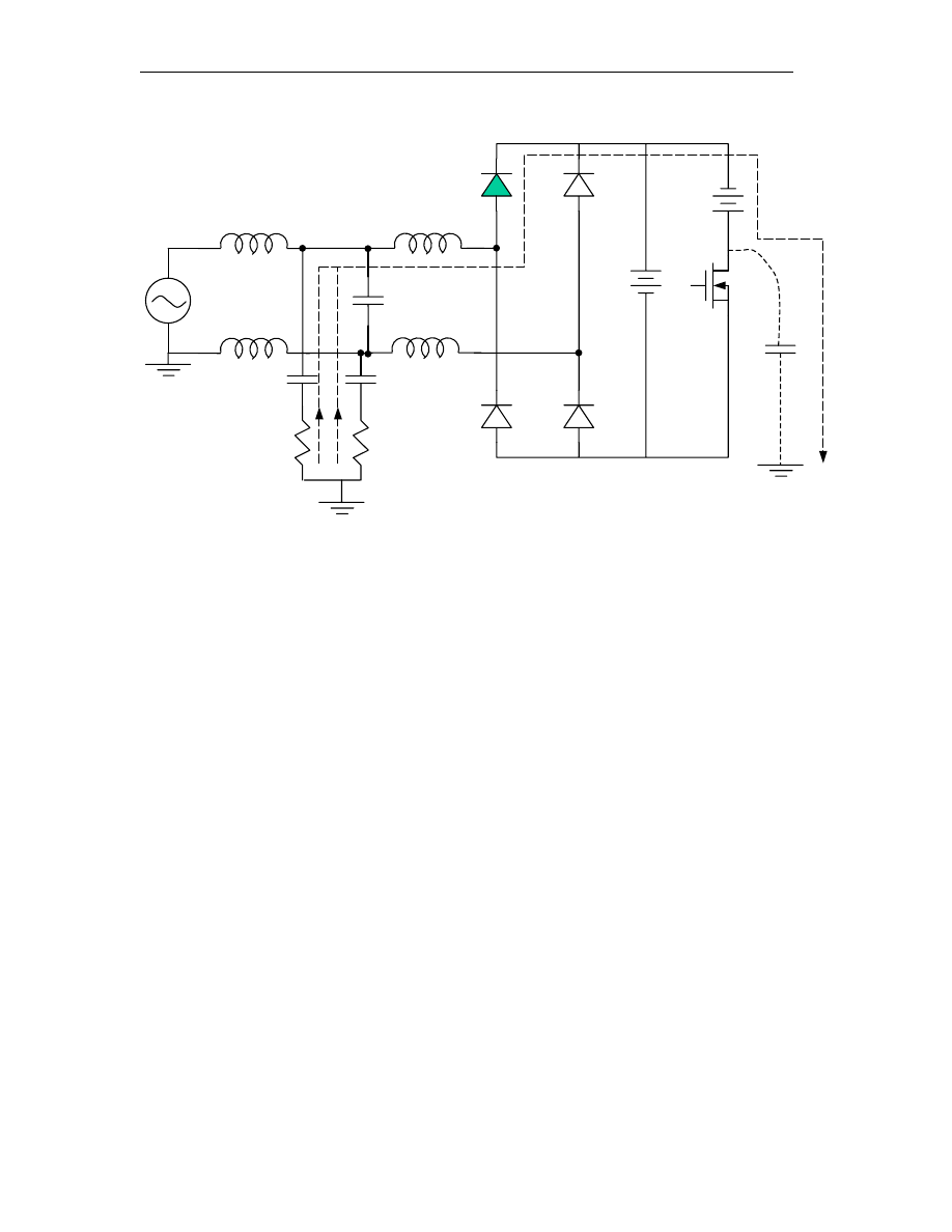
3.1.2 Effect of Asymmetrical DM Choke
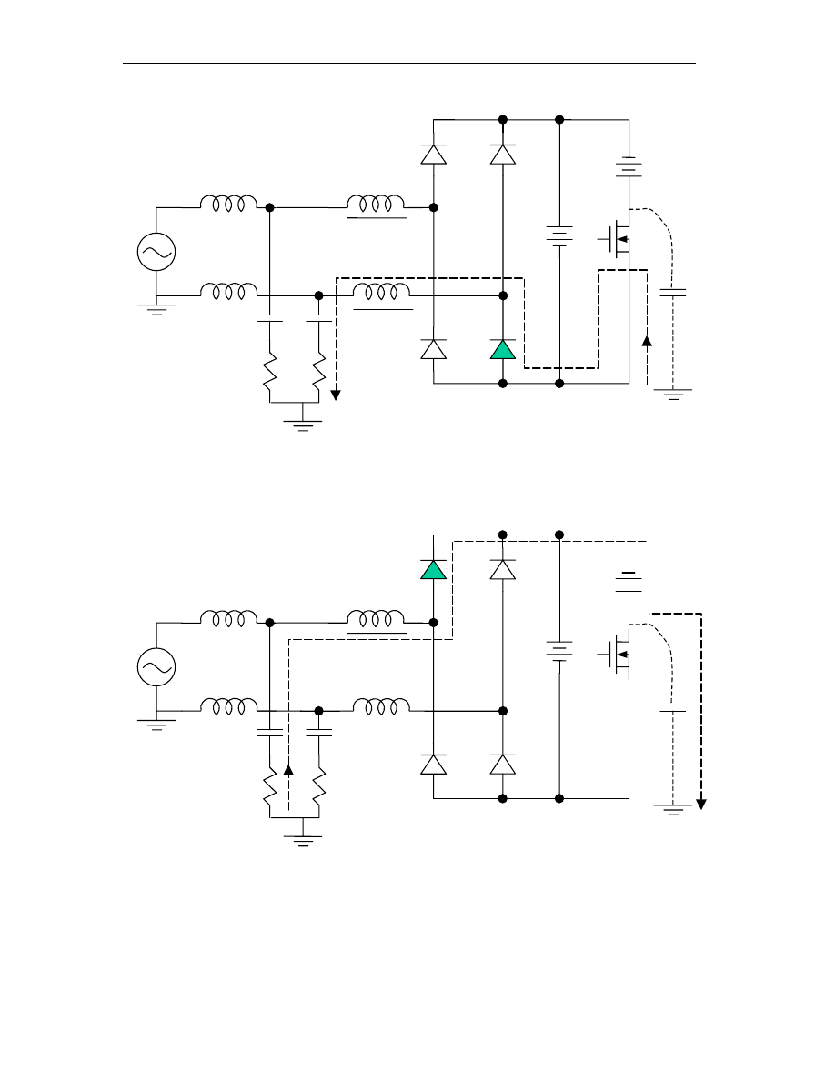
(a) Rectifier Diodes Off, MOSFET Being Turned On (Cp Discharged)
(b) Rectifier Diodes Off, MOSFET Being Turned Off (Cp Charged)
Fig.3-3 Noise Path Models with Asymmetrical DM Chokes
Cp
A
B
DM Choke
LISN
R1
R2
D1
D2
D4
D3
Cp
A
B
DM Choke
LISN
D1
D2
D3
D4

Non-Intrinsic Differential Mode Noise of Switching Power Supplies and Its Implications to Filter Design
28
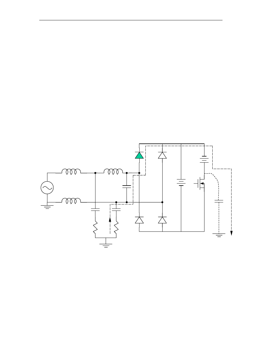
The phenomenon can be explained from the noise model shown in Fig.3-3. Fig.3-3
(a) shows the case of asymmetrical DM choke when MOSFET is being turned off and
parasitic capacitance Cp is being charged. The charging current flowing through R1 sees
the inductance and the noise current can be suppressed. Fig.3-3 (b) shows the situation
when rectifier is “off” and MOSFET is being turned on. Noise paths are unbalanced and
NIDM still exists. Notice that most of the ground noise flows through D3 and R2 without
seeing DM inductor. Therefore, the DM choke has no attenuation for the noise in that
case. Fig.3-4 shows that although IDM can be suppressed by the asymmetrical DM
choke, the amplitude of NIDM does not change. If NIDM is dominant in total DM
spectrum, then the DM noise envelope will not change after the use of an asymmetrical
DM choke.
Notice that the two waveforms are supposed to coincide on both trailing edges. In
fact, the waveform marked as “DM with asymmetrical choke” was purposely displayed
with some delay to see the waveforms better.
Non-Intrinsic Differential Mode Noise of Switching Power Supplies and Its Implications to Filter Design
29
Fig.3-4 DM Noise with Asymmetrical DM Choke (Zero Span Mode)
The waveform of “DM with asymmetrical choke” was purposely delayed for the
convenience of observation.
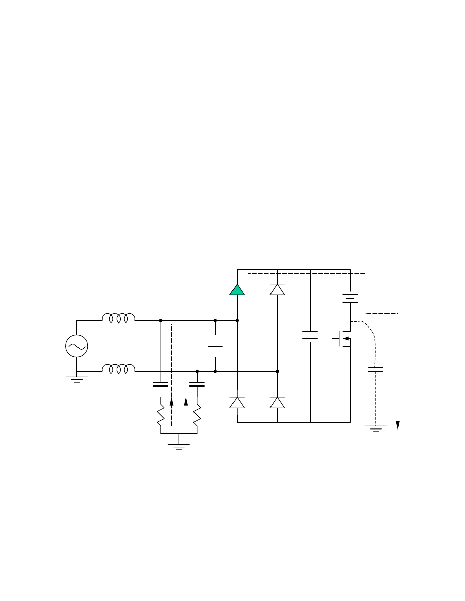
3.1.3 Effect of Symmetrical DM Choke
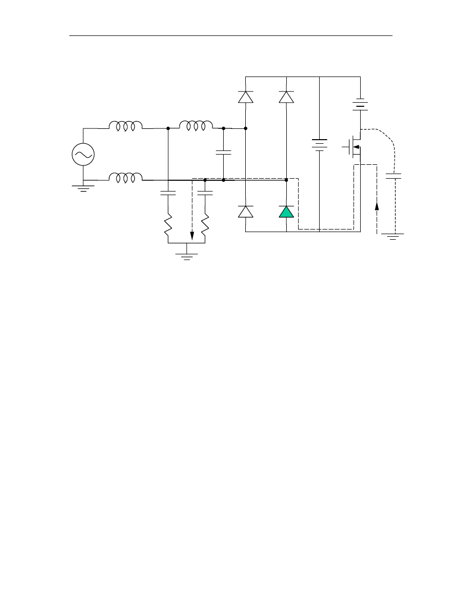
From above analysis, we know that asymmetrical filter topology can also contribute
to the generation of NIDM. To verify this conclusion, we split the 1.2mH DM choke into
two 600
ÿH chokes as shown in Fig.3-1 (b). From Fig.3-2 (b), we can see DM noise
attenuation of the symmetrical filter topology is significant, especially for high frequency
range. This can also be explained using noise path models shown in Fig.3-5. Fig.3-5 (a)
shows the situation when rectifier diodes are off and the MOSFET is being turned off.
DM without Choke
DM with Asymmetrical Choke
Delay
Non-Intrinsic Differential Mode Noise of Switching Power Supplies and Its Implications to Filter Design
30
(a) Rectifier Diodes Off, MOSFET Being Turned Off (Cp Discharged)
(b) Rectifier Diodes Off, MOSFET Being Turned Off (Cp Charged)
Fig.3-5 Noise Path Models with Symmetrical DM Chokes
Cp
A
B
LISN
D1
D2
D3
D4
Cp
A
B
LISN
D1
D2
D3
D4

Non-Intrinsic Differential Mode Noise of Switching Power Supplies and Its Implications to Filter Design
31
Fig.3-5 (b) illustrates the situation when rectifier diodes are off and the MOSFET is
being turned off. The noise paths are unbalanced in this case. But we can see no matter
which path the noise current takes, it will always see a DM choke in the path and the
ground noise current can then be suppressed by the inductance.
This conclusion is extremely critical to filter design. When designers choose filter
topologies, they usually do not pay much attention to the symmetry of the filter, even
though they know empirically that symmetrical topology is better than asymmetrical one.
The above experiment has demonstrated clearly the advantage of symmetrical filter
topology in suppressing NIDM.
3.2 Effect of X Capacitor on NIDM
The NIDM noise discussed so far is of the same generation mechanism: the
impedance unbalance of the two noise current paths during rectifier diodes “off” period.
If the impedance of one path is much higher than that of the other path, more noise
current will flow through the lower impedance path and cause higher voltage drop across
one of the LISN resistors. DM noise is defined earlier as the difference between the noise
voltages across both LISN branches (DM = (Vx-Vy)). Therefore, a significant amount of
DM noise will be measured if the noise paths are unbalanced. The best way to filter this
noise is to balance the noise current paths so that the current can be distributed evenly
between both LISN resistors during parasitic capacitor Cp charging and discharging.
Non-Intrinsic Differential Mode Noise of Switching Power Supplies and Its Implications to Filter Design
32
To balance the two current paths, a capacitor Cx, which is usually known as X
capacitor can be connected between points A and B as shown in Fig.3-6 (a) and Fig.3-6
(b). For high frequency noise current, the impedance of the capacitor is very low. Cx is
essentially shorted if the capacitance is large enough. The unbalanced situation described
above can be corrected because high frequency noise current can flow evenly through
both of the LISN branches during both MOSFET “on” and “off” transients. The paths for
ground noise current will become balanced. The noise voltage difference between the two
LISN branches is small and the NIDM noise is attenuated significantly.
(a) Rectifier Diodes Off, MOSFET Being Turned Off (Cp Charged)
Cp
Cx
A
B
Non-Intrinsic Differential Mode Noise of Switching Power Supplies and Its Implications to Filter Design
33
(b) Rectifier Diodes Off, MOSFET Being Turned On (Cp Discharged)
Fig.3-6 Balancing Noise Paths with X Capacitor
In each case, the noise current paths have been balanced due to the low impedance
path provided by the X capacitor.
Using zero span mode of spectrum analyzer, we can find changes in NIDM noises
due to adding an X capacitor between point A and point B. The measurement result is
shown in Fig.3-7. The upper trace is the differential mode noise of EUT without adding
X capacitor. The lower trace is the differential mode noise of EUT with a 0.33
µ
F X
capacitor connected right next to the bridge rectifier. As described earlier, time interval
“A” corresponds to the rectifier “off” period, interval “B” corresponds to the rectifier
“on” period. From previous analysis, we know in interval A, the DM noise is essentially
NIDM while in interval B the noise is IDM.
Cp
Cx
A
B
Non-Intrinsic Differential Mode Noise of Switching Power Supplies and Its Implications to Filter Design
34
Fig.3-7 Effect of X Capacitor on NIDM in Zero Span Mode
Interval A: Rectifier Diodes Off (NIDM)
Interval B: Rectifier Diodes On (IDM)
A
B
Without X Cap
With 0.33
µ
F X Cap
0
30
Time (ms)
Non-Intrinsic Differential Mode Noise of Switching Power Supplies and Its Implications to Filter Design
35
(a) DM Noise without X Capacitor
(b) DM Noises with X Capacitor
Fig.3-8 Effect of X Capacitor on NIDM in Frequency Domain

Non-Intrinsic Differential Mode Noise of Switching Power Supplies and Its Implications to Filter Design
36
From Fig.3-7, We can see the X capacitor has little attenuation on IDM (less than 3
dB). This can be justified by the characteristics of IDM noise source. The noise source
impedance of IDM is usually very low, so a capacitor in parallel is not effective as an
inductive filter. However, the attenuation for NIDM is significant (almost 15 dB) because
of the balanced noise paths. The total DM reduction after adding Cx is shown in Fig.3-8.
The DM noise reduction after adding X capacitor is very significant. To balance the noise
current paths, the impedance of the X capacitor should be as low as possible. But on the
other hand, lower impedance means higher capacitance value and larger size, which is
undesirable in filter design. That issue will be addressed in Section 3.5 of this chapter.
Another question regarding balancing noise paths with X cap is: “Does adding X cap
increase the CM noise?” Because it seems like the X cap changes NIDM into CM. The
answer to that question is no. Fig.3-9 shows the CM measurement results before and after
adding X cap. CM noise level keeps to be the same for both cases. CM noise is the
average of Vx and Vy. In unbalanced case, one voltage is much higher than the other one.
When the noise paths are balanced, the two voltages become the same value. But the
summation of these two voltages will not change because during steady state operation,
the total charge of the parasitic capacitor Cp is constant for each switching cycle.
Non-Intrinsic Differential Mode Noise of Switching Power Supplies and Its Implications to Filter Design
37
(a) CM Noise without X Capacitor
(b) CM Noise with X Capacitor
Fig.3-9 Effect of X Capacitor on CM Noise
CM Noise
CM Noise

Non-Intrinsic Differential Mode Noise of Switching Power Supplies and Its Implications to Filter Design
38
3.3 Position of X Capacitor in Filter
The use of X capacitors can effectively attenuate NIDM noises caused by noise path
unbalance as discussed in Section 3.2. But from earlier discussion, we know X capacitor
by itself has little attenuation effect on IDM noise that is usually caused by the harmonic-
rich input current. Other filter elements must be used together with the X capacitor to get
a better suppression of all the DM noise components. Because of the low source
impedance nature of IDM noise, the filter for IDM must consist of at least one inductive
element. A commonly asked question is: if such an inductor-capacitor filter topology is
used, should the X capacitor be placed on the LISN side or on the EUT side of the
circuit? The answer is that it depends on whether symmetrical choke or asymmetrical
choke is used. This will be discussed below
3.3.1 Asymmetrical Inductor with X Capacitor
The DM filter consists of two components: a single-side DM asymmetrical choke and
an X capacitor. There are two possible filter topologies depending on the position of X
capacitor. In one topology, the X capacitor is adjacent to EUT and in the other, X
capacitor is right next to LISN as shown in Fig.3-10(a) and Fig.3-10(b). To distinguish
these two topologies, we call the first one “LC” filter and the second one “CL” filter.
Non-Intrinsic Differential Mode Noise of Switching Power Supplies and Its Implications to Filter Design
39
(a) X Capacitor on EUT Side (LC Filter)
(b) X Capacitor on LISN Side (CL Filter)
Fig.3-10 Two Asymmetrical DM Filter Topologies
Cp
Cx
A
B
DM Choke
Cp
Cx
A
B
DM Choke
Non-Intrinsic Differential Mode Noise of Switching Power Supplies and Its Implications to Filter Design
40
3.3.1.1 Asymmetrical Filter Topology with X Cap on EUT Side
First, consider the topology with X capacitor adjacent to EUT. Using a simplified
noise emission model shown in Fig.3-11 (a) and Fig.3-11 (b), the ground noise current
paths can be found.
(a) Switch Being Turned Off (Cp Charged)
Cp
Cx
A
B
DM Choke
Non-Intrinsic Differential Mode Noise of Switching Power Supplies and Its Implications to Filter Design
41
(b) Switch Being Turned On (Cp Discharged)
Fig.3-11 Noise Path Model: Asymmetrical DM Choke, X Capacitor on EUT Side,
Rectifier Diodes Off in Both Cases
Fig.3-11 (a) shows the NIDM noise path when the switch is being turned off and (b)
shows the noise path when the switch is being turned on. It can be seen that no matter
whether the switch is being turned on or off, the two noise current paths have different
impedance values even though the X capacitor has been added. The difference in
impedance values is caused by the existence of asymmetrical DM choke. The noise path
with DM choke is higher in impedance and less noise current and the other path is lower
in impedance and more noise current flowing through. The noise current difference
between these two paths becomes NIDM noise. Fig.3-12 is the DM noise captured with
zero-span mode. The upper trace was measured when only a DM choke was inserted
Cx
A
B
DM Choke
Non-Intrinsic Differential Mode Noise of Switching Power Supplies and Its Implications to Filter Design
42
between LISN and EUT. The lower trace was measured when both DM choke and an X
capacitor were used, and the X capacitor is next to EUT. Again, the shift of the bottom
waveform is purposely done for better view of the two waveforms. One can see from this
figure that NIDM part is reduced by some amount but not much.
Fig.3-12 DM with Asymmetrical Choke and X Cap on EUT Side
From Fig.3-12, we can see the reduction of NIDM noise is not obvious after adding
an X capacitor. The total frequency domain spectrum of DM noise also gives us the same
result, which is shown in Fig.3-13.
DM with asymmetrical choke,
without X cap
DM with asymmetrical choke
and X cap on EUT side
Time (ms)
0
30
Non-Intrinsic Differential Mode Noise of Switching Power Supplies and Its Implications to Filter Design
43
(a) DM Noise with Asymmetrical DM Choke (No X Cap)
(b) DM Noise with Asymmetrical DM Choke and X Capacitor on EUT Side
Fig.3-13 DM Noise with Asymmetrical Choke and 0.33
µ
F X Cap on EUT Side
Non-Intrinsic Differential Mode Noise of Switching Power Supplies and Its Implications to Filter Design
44
3.3.1.2 Asymmetrical Filter Topology with X Cap on LISN Side
Consider the topology with X capacitor on LISN side. The noise paths are shown in
Fig.3-14(a) and Fig.3-14 (b).
(a) Switch Being Turned Off
(b) Switch Being Turned On
Fig.3-14 Noise Path Model: Symmetrical Choke and X Cap on LISN Side
Cp
Cx
A
B
DM Choke
Cp
Cx
A
B
DM
Non-Intrinsic Differential Mode Noise of Switching Power Supplies and Its Implications to Filter Design
45
Fig.3-14 (a) shows the noise path when the switch is being turned off and (b) shows
the noise path when the switch is being turned on. It can be seen that whether the switch
is being turned on or off, the noise current paths have almost the same impedance values.
Adding an X capacitor right next to the LISN reduces NIDM noise much more
effectively than otherwise. Fig.3-15 is the DM noise captured with zero-span mode of
spectrum analyzer. The upper trace was measured when only a DM choke was inserted
between LISN and EUT. The lower trace was measured when both DM choke and X
capacitor were used, and the X capacitor is next to LISN.
The NIDM reduction is
significant (about 30dB compared to 6dB in Fig.3-12).
Fig.3-15 DM with Asymmetrical Choke and X Cap at LISN Side (Zero-Span Mode)
DM with asymmetrical
c
hoke, no X cap
DM with asymmetrical choke and X cap
on LISN
s
ide
Time (ms)
0
30
Non-Intrinsic Differential Mode Noise of Switching Power Supplies and Its Implications to Filter Design
46
As a conclusion, it is shown that placing the X capacitor on the LISN side is more
effective to suppress the NIDM than otherwise if asymmetrical choke is used.
3.3.2 Symmetrical Inductor with X Capacitor
Fig.3-16 and Fig.3-17 show the noise current paths for the two possible filter
topologies with a symmetrical DM choke are used. The X capacitor is put on EUT side in
Fig.3-16 and on LISN side in Fig.3-17.
(a) Rectifier Diodes Off, MOSFET Turned On (Cp Discharged)
Cp
Cx
A
B
DM Choke
DM Choke
Non-Intrinsic Differential Mode Noise of Switching Power Supplies and Its Implications to Filter Design
47
(b) Rectifier Diodes Off, MOSFET Turned Off (Cp Charged)
Fig.3-16 Noise Path Model with X Cap on EUT Side
(a) Rectifier Diodes Off, MOSFET Turned On (Cp Discharged)
Cp
Cx
A
B
DM Choke
DM Choke
Cp
Cx
A
B
DM Choke
DM Choke
Non-Intrinsic Differential Mode Noise of Switching Power Supplies and Its Implications to Filter Design
48
(b) Rectifier Diodes Off, MOSFET Turned Off (Cp Charged)
Fig.3-17 Noise Path Model with X Cap on LISN Side
From the noise path models, it is clear that if the filter topology is symmetrical, the X
capacitor will have same effect no matter whether it is placed on the LISN side or the
EUT side. Because in either case, there are balanced currents through the two LISN
resistors during Cp charging and discharging, the NIDM noise is reduced by large
amount. This conclusion can be verified by the following experimental results, which are
shown in Fig.3-18.
Cp
Cx
A
B
DM Choke
DM Choke
Non-Intrinsic Differential Mode Noise of Switching Power Supplies and Its Implications to Filter Design
49
(a) X Cap on LISN Side
(a) X Cap on LISN Side
(b) X Cap on EUT Side
(b) X Cap on EUT Side
Fig.3-18 DM Noise with Symmetrical Choke and X Cap
Symmetrical choke with X cap
on LISN side
Symmetrical choke without X cap
Symmetrical choke without X cap
Symmetrical choke with X cap
on EUT side
Non-Intrinsic Differential Mode Noise of Switching Power Supplies and Its Implications to Filter Design
50
3.4 Effect of CM Chokes on NIDM
Conventionally, theory says that CM choke has no suppressing effect on DM noise
except that the leakage inductance of the CM choke should have some effect on DM
noise. This is true, however, only for IDM. For NIDM, CM should have suppressing
effect when the two paths are unbalanced, i.e. without a balancing capacitor Cx. Fig.3-19
shows the experimental setup.
Fig.3-19 Experiment Setup for CM Choke Effect
Cp
A
B
CM Choke
0.7mH
Non-Intrinsic Differential Mode Noise of Switching Power Supplies and Its Implications to Filter Design
51
Fig.3-20 shows the effect. Notice that for IDM portion (interval B), the suppression
due to CM choke is minor, which supports conventional EMI theory. However, the
attenuation of the NIDM portion (interval A) is very pronounced. Even though noise
current is unbalanced as shown in Fig.3-19, but the magnitude of both currents are
attenuated already by the CM choke whether D1 or D3 conducting and therefore, the
NIDM noise is small. Since CM choke is normally much larger than DM choke in
inductance, therefore, CM choke can suppress the NIDM noise effectively also. Fig.3-19
shows the total DM noise attenuation.
Fig.3-20Effect of CM Choke on NIDM (Zero-Span Mode)
Fig.3-21 shows the comparison of total DM noise spectrum with and without CM choke.
DM without CM Choke
DM with CM Choke
A
B
Interval a: NIDM
Interval b: IDM
Non-Intrinsic Differential Mode Noise of Switching Power Supplies and Its Implications to Filter Design
52
(a) Without CM Choke
(b) With 0.7mH CM Choke
Fig.3-21 Effect of CM Choke on DM Noise
Non-Intrinsic Differential Mode Noise of Switching Power Supplies and Its Implications to Filter Design
53
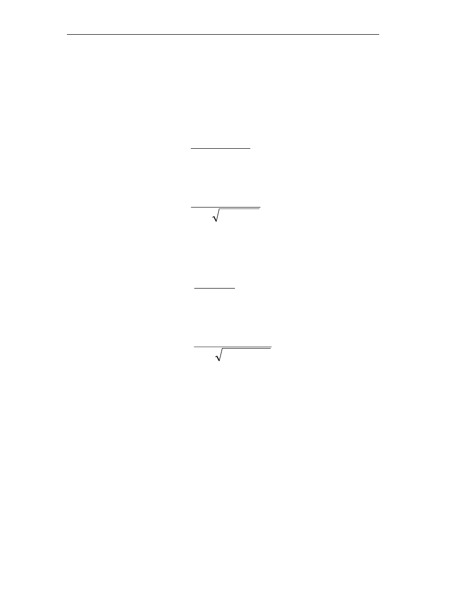
3.5 Determination of Balancing Cap (X Cap) Value
To effectively suppress the NIDM noise, the balancing capacitor should provide
balanced impedance such that the currents flowing through the two LISN resistors R1
and R2 are about the same whether Cp is charged or discharged. Under this condition, the
choice of Cx value depends on frequency and the filter topology. The discussion is given
below.
(A) When Cx is placed on the LISN side as shown in Fig3-22, then the condition is
Where f is the start frequency of EMI noise specs (150 kHz for VDE and 450 kHz for
FCC). As long as the Eq. (1) holds, the two current paths are balanced. This is true
whether there is DM choke or CM choke in the filter.
Fig.3-22 X Capacitor on LISN Side
Ω
<<
50
2
1
X
fC
π
)
1
(
Cp
CM Choke
A
B
DM Choke
Cx
Non-Intrinsic Differential Mode Noise of Switching Power Supplies and Its Implications to Filter Design
54
(B) When Cx is on the EUT side as shown in Fig3-23, the condition is
Where L
D
is the DM choke inductance of each line and L
C
is the CM choke inductance.
As explained in Section 3.3, using symmetrical choke L
D
on both lines is effective. From
Eq. (1) and (2), it can be seen that Cx can be much smaller, if Cx is placed on the EUT
side when chokes are used in the filter.
Fig.3-23 X Capacitor on EUT Side
)
(
2
50
2
1
C
D
X
L
L
f
j
fC
+
+
<<
π
π
)
2
(
Cp
A
B
CM Choke
DM Choke
Cx
Non-Intrinsic Differential Mode Noise of Switching Power Supplies and Its Implications to Filter Design
55
Fig.3-24 (a) shows the NIDM suppressing effect when a 0.022
µ
F X capacitor is used:
And Fig.3-24 (b) for the case when a 0.33
µ
F X capacitor is used:
(a) DM with 0.022
µ
F X Cap on LISN Side
(Trace B is delayed purposely for a better view)
Ω
≅
×
×
×
×
=
−
50
10
022
.
0
10
150
28
.
6
1
2
1
6
3
X
fC
π
Ω
×
≅
×
×
×
×
=
−
50
10
1
10
33
.
0
10
150
28
.
6
1
2
1
6
3
X
fC
π
NIDM
IDM
NIDM
IDM
Trace A
Trace B
delay
Trace A: without X cap
Trace B: with 0.022
µ
F X cap
Non-Intrinsic Differential Mode Noise of Switching Power Supplies and Its Implications to Filter Design
56
(b) DM with 0.33
µ
F X Cap on LISN Side
Fig.3-24 Impedance of X Cap Affects NIDM Attenuation
Fig.3-25 confirms that when Cx on the EUT side is more effective in the case when
DM chokes or CM chokes are placed in the filters. The inductance of the CM choke is
150
µ
H in the following example.
(a) Experimental Configuration
NIDM
IDM
Without X Cap
With 0.33
µ
F X Cap
LISN
EUT
150
µ
H
0.022
µ
F
LISN
EUT
150
µ
H 0.022
µ
F
Non-Intrinsic Differential Mode Noise of Switching Power Supplies and Its Implications to Filter Design
57
(b) Experimental Result
Fig.3-25 Same X Cap on LISN Side or EUT Side
IDM
NIDM
X cap on LISN side
X cap on EUT side
Cx=0.022
µ
F, Lc=150
µ
H

Non-Intrinsic Differential Mode Noise of Switching Power Supplies and Its Implications to Filter Design
58
Chapter 4 EMI Filter Design Incorporating NIDM
4.1 Basis for EMI Filter Design
In view of the NIDM phenomenon described in Chapter 3, the conventional filter
design procedure needs modification. The end result of the modification is smaller
differential-mode filter. A design example will be given and verified in this chapter.
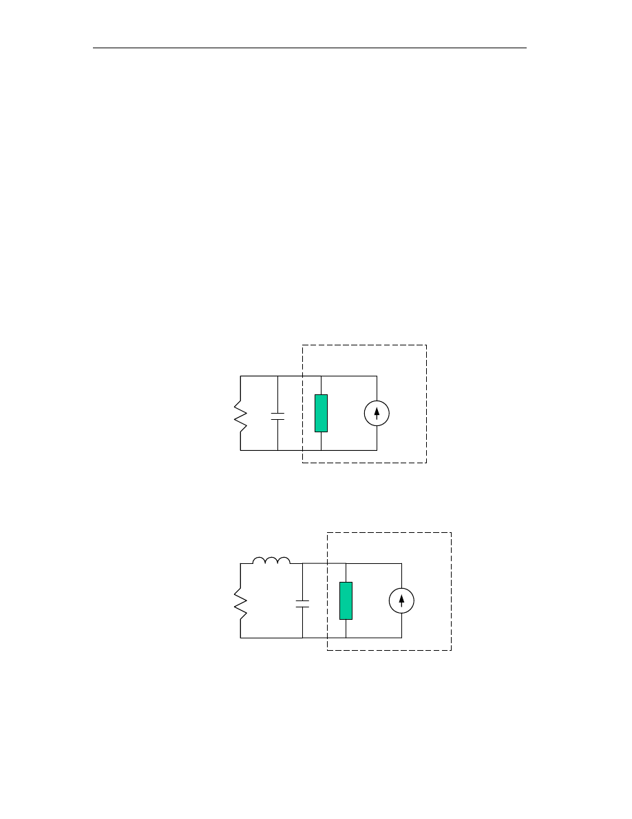
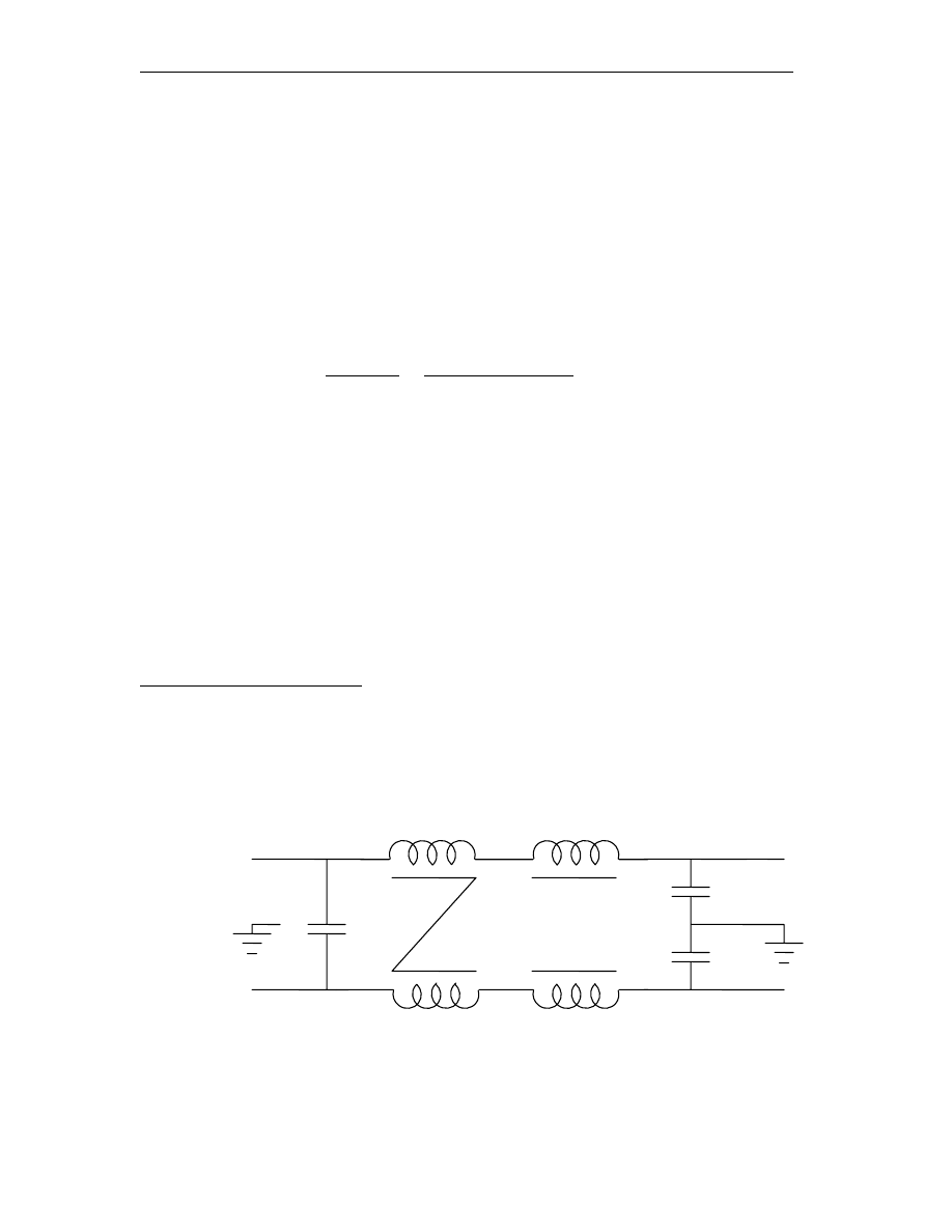
4.1.1 Noise Source Impedance
Because NIDM noise can be suppressed by CM choke and balancing capacitor, the
main concern in EMI filter design is CM and IDM noise. The equivalent circuit model of
CM noise source is a current source with high parallel impedance, and the model of IDM
source is a voltage source with low series impedance as shown in Fig.4-1 (a) and (b)
respectively.
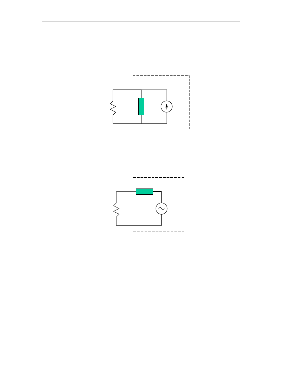
Non-Intrinsic Differential Mode Noise of Switching Power Supplies and Its Implications to Filter Design
59
(a) CM Noise Source
(b) IDM Noise Source
Fig.4-1 Equivalent Model of Noise Sources
4.1.2 Possible Filter Topologies
Based on the characteristics of noise source impedance, the effective filter component
arrangement can be found. Only first and second order filters are discussed in this
section. The filter topologies of higher orders are beyond the scope of this thesis.
Zs
V
IDM
LISN
Resistor
IDM Noise Source
Zp
V
CM
LISN
Resistor
CM Noise Source
Non-Intrinsic Differential Mode Noise of Switching Power Supplies and Its Implications to Filter Design
60
For noise sources of high impedance, such as CM source, the effective way of
attenuation is to use a low impedance element in parallel with the noise source. Because
capacitors can provide low impedance at high frequency, the single capacitor filter is the
most effective first-order topology for CM noise source. Sometimes, an additional filter
element is used to increase the impedance mismatch. That element should provide high
impedance in series with the load. Because inductors have high impedance at high
frequency, the inductor-capacitor topology with the capacitor adjacent to the noise source
is the most effective second-order filter for CM. That topology is called LC filter in this
thesis. The topologies are shown in Fig.4-2.
(a) First-Order
(b) Second-Order
Fig.4-2 Effective Filter Topologies for CM Noise
Zp
V
CM
LISN
Resistor
CM Noise Source
C
Zp
V
CM
LISN
Resistor
CM Noise Source
C
L
Non-Intrinsic Differential Mode Noise of Switching Power Supplies and Its Implications to Filter Design
61
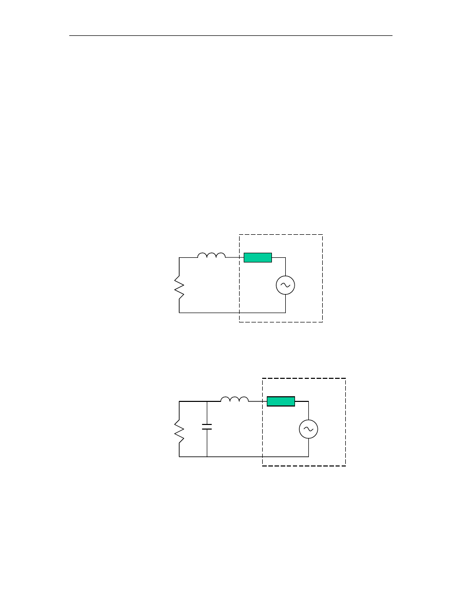
For noise sources of low impedance, such as IDM source, the effective way of
attenuation is to use a high impedance element series with the noise source. The single
inductor filter is the most effective first-order topology for IDM noise source. For
second-order topology, the additional element should provide low impedance in parallel
with the load. The inductor-capacitor topology with the inductor adjacent to the noise
source is the most effective second-order filter for IDM. That topology is called CL filter
to distinguish it from the one used for CM source. The topologies are shown in Fig.4-3.
(a) First-Order Filter
(b) Second-Order Filter
Fig.4-3 Effective Topologies for IDM Source
Zs
V
IDM
LISN
Resistor
IDM Noise Source
L
C
Zs
V
IDM
LISN
Resistor
IDM Noise Source
L
Non-Intrinsic Differential Mode Noise of Switching Power Supplies and Its Implications to Filter Design
62
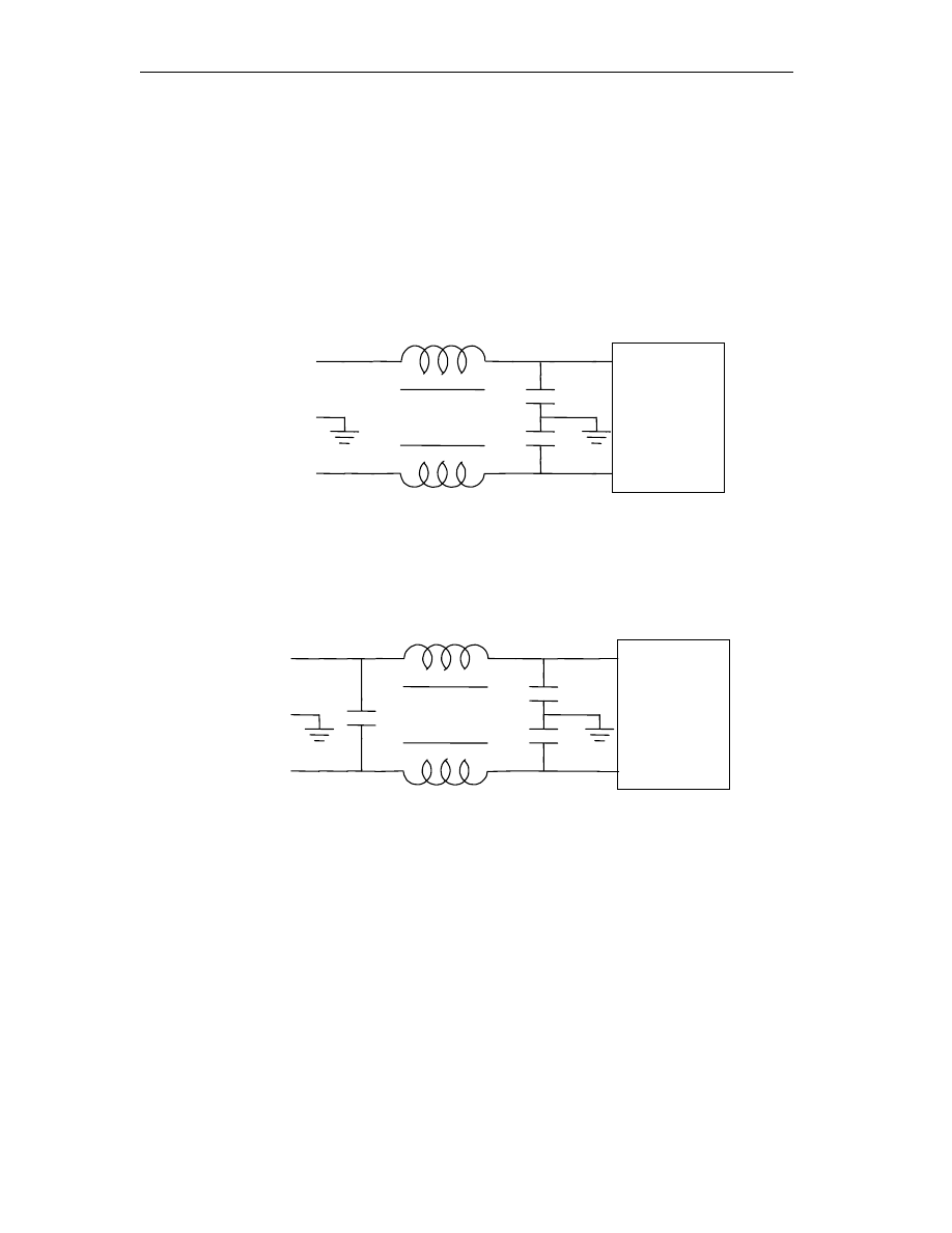
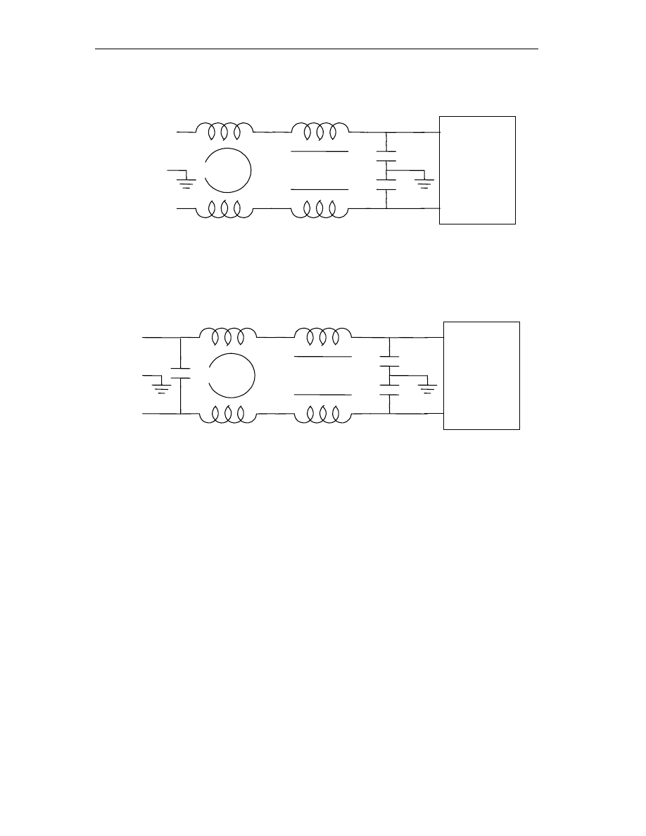
The complete EMI filter is the combination of CM section and DM section. There are
four available topologies, which comply with the above arrangement rules. Fig.4-4 shows
these four filters.
(a) First-Order CM and First-Order DM
(b) First-Order CM and Second-Order DM
L
G
N
DM Choke
Cy
Cy
EUT
L
G
N
DM Choke
Cx
Cy
Cy
EUT
Non-Intrinsic Differential Mode Noise of Switching Power Supplies and Its Implications to Filter Design
63
(c) Second-Order CM and First-Order DM
(d) Second-Order CM and Second-Order DM
Fig.4-4 Available EMI Filter Topologies
4.2 Determine the Position of X Capacitor
According to the discussion in Section 4.2, the X capacitor will be more effective if it
is place on the LISN side because of the low source impedance of IDM noise source. But
if NIDM is considered and symmetrical filter topology being used, X cap on the EUT
side is a better choice. Fig.4-5 summarizes the comparison result.
L
G
N
CM Choke
DM Choke
Cy
Cy
EUT
L
G
N
CM Choke
DM Choke
Cy
Cy
Cx
EUT
Non-Intrinsic Differential Mode Noise of Switching Power Supplies and Its Implications to Filter Design
64
Fig.4-5 Comparison of X Cap on LISN Side and on EUT Side
When determining the position of X cap, several issues need to be considered
simultaneously. If asymmetrical filter topology is being used, then the X capacitor should
always be placed on the LISN side. If symmetrical filter topology is used, the position of
X capacitor will depend on the DM noise components. If IDM is dominant over NIDM,
the X capacitor should be placed on the LISN side and if NIDM is dominant, the
capacitor should be on the EUT side of the filter.
LISN
EUT
LISN
EUT
IDM
NIDM
More
Effective
Less
Effective
Less
Effective
More
Effective

Non-Intrinsic Differential Mode Noise of Switching Power Supplies and Its Implications to Filter Design
65
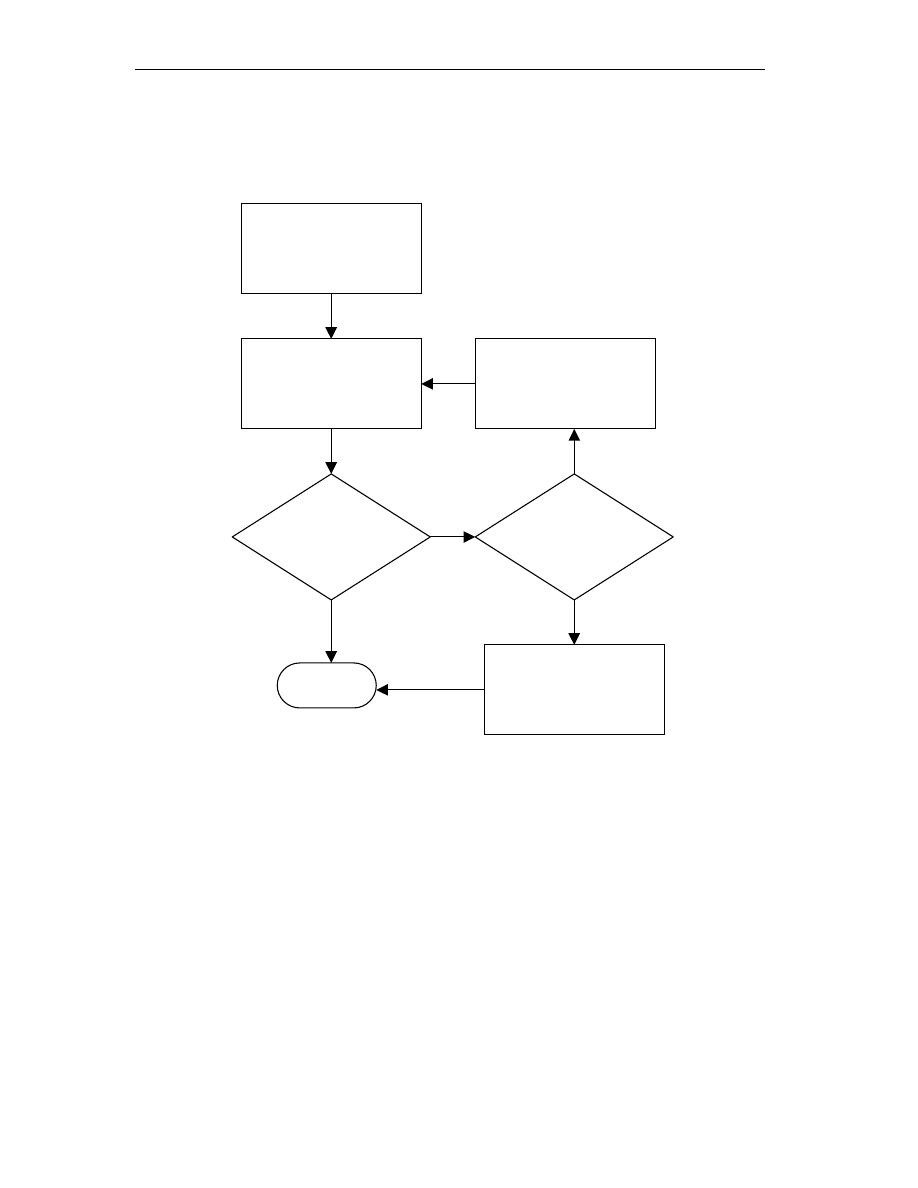
4.3 EMI Filter Design Procedure
From the previous discussions, it is clear that it is extremely difficult to obtain an EMI
filter design analytically. A practical approach was proposed in [3] to deal with the
difficult issue. The approach was based on the following three conditions:
(1) Baseline (i.e. without filter) EMI noise for both CM and DM must be provided.
(2) If the filter elements are properly arranged and sized, source impedance has little
effect. Therefore, analytical design is possible without knowing exactly the source
impedance values.
(3) The focus of the design procedure is to meet the low frequency specification.
After the filter is designed and built, high-frequency performance can be tuned if
necessary.
The above assumptions lay down the ground for a possible analytical filter design
procedure. The flow chart of the design procedure is shown in Fig.4-6. But the method in
[3] has its own limitation. In that approach, only one typical filter topology is considered.
Although the topology is the most commonly used filter, it cannot be the optimum one
for every power supply. So a complete design procedure should be able to consider other
filter topologies. Another limitation about that method is that the mechanism and
characteristics of NIDM are not being considered in the design procedure.
To overcome these limitations, a new design procedure will be proposed in the
present thesis. The new procedure can be regarded as an expansion of the old procedure,
because the theoretical bases are the same for both methods.
Non-Intrinsic Differential Mode Noise of Switching Power Supplies and Its Implications to Filter Design
66
Fig.4-6 Flow Chart for Filter Design
An EMI filter basically consists of two sections: CM section and DM section. These
two sections can be designed independently. In Block I of the flow chart, filter
attenuation requirements for CM and DM noise are obtained first. This involves the use
of noise separator for noise baseline measurement for both CM and DM noise. From
Obtain Attenuation
Requirement
Determine Filter
Component Values
Meet Spec.
For Both Low & High
Freq.?
End
If Low Freq.
Spec. Not Met?
Lower the Filter
Corner Frequency
Block I
Block II
Tune for High
Frequency
Performance
Block III
Yes
No
Yes
No

Non-Intrinsic Differential Mode Noise of Switching Power Supplies and Its Implications to Filter Design
67
previous discussion, we know balancing noise paths can significantly attenuate NIDM
noise. Then the DM section of the filter will solely deal with IDM noise. Therefore, the
baseline of IDM noise should be provided. But it is very difficult to separate IDM noise
from NIDM noise. One possible solution is to use an X capacitor to balance the noise
paths and then measure the DM noise using a noise separator. Because the NIDM has
been attenuated by the X capacitor, the remaining DM noise will be IDM. The value of
capacitance can be chosen using the method introduced in the previous chapter. Based on
the information obtained in Block I, topologies and component values of CM and IDM
sections of the EMI filter can be determined in Block II. First, we consider low order
filters, such as first-order ones. According to the attenuation curves obtained in Block I,
the corner frequency of the filter can be determined. The component values can then be
calculated. If the component values are impracticably large, which means filters of higher
orders should be used, then we increase the order and recalculate the corner frequency
and component values until reasonable component values and attenuation are obtained.
This design is mainly to meet the low frequency specification. Theoretically speaking,
the filter design obtained in Block II should meet both the low frequency and high
frequency specifications. However, many high frequency effects, which are difficult to
predict at the design stage of EMI filters, may cause the violation of design specification
at high frequency. Block III provides some possible causes of the high frequency
performance degradation, which include high frequency parasitic effects of filter
components, permeability roll-off of magnetic material, radiation coupling problems and
filter-source impedance interaction.
The design procedure can be summarized into following steps.

Non-Intrinsic Differential Mode Noise of Switching Power Supplies and Its Implications to Filter Design
68
Step 1: Measure baseline EMI emission including total noise, CM noise, DM noise
and IDM noise. For CM and DM noise measurement, a noise separator is needed. For
IDM measurement, an X capacitor is besides the noise separator. The value of the
capacitor should be large enough to balance the noise paths.
Step 2: Determine attenuation requirements. The required attenuation is the
discrepancy between the baseline noise and the EMI specs plus some correction factor.
The correction factor has been discussed previously. It is “+3dB” for CM and IDM
attenuation.
Step 3: Choose filter topology. This step also includes determining the order of the
filter. Because of the nature of CM and DM noise source impedance, we don’t have many
choices on topology when the order is determined. All the possible choices have been
shown in the Fig.4-4.
Step 4: Determine filter corner frequencies. The attenuation curve of a filter can
usually be approximated to a straight line with certain slope when the frequency is
beyond the filter corner frequency. The slope is 20dB/decade for first-order filter,
40dB/decade for second-order and 60dB/decade for third-order. To obtain the corner
frequency, we can draw such a line and make it tangent to the attenuation curves obtained
in Step 2. The horizontal intercept of the line determines the filter corner frequency.
dB
V
V
V
spec
CM
req
CM
3
,
+
−
=
dB
V
V
V
spec
IDM
req
IDM
3
,
+
−
=
Non-Intrinsic Differential Mode Noise of Switching Power Supplies and Its Implications to Filter Design
69
Step 5: Determine filter component values. After determining the filter corner
frequency, the filter component values can be calculated using the equations given below.
The derivation of these equations are given in the appendix.
First Order CM Filter
25
2
2
1
,
⋅
⋅
=
Y
CM
R
C
f
π
(4-1)
Second Order CM Filter
Y
C
CM
R
C
L
f
2
2
1
,
⋅
⋅
=
π
(4-2)
First Order DM Filter
D
IDM
R
L
f
2
2
100
,
⋅
=
π
(4-3)
Second Order DM Filter
X
D
IDM
R
C
L
f
⋅
⋅
⋅
=
2
2
1
,
π
(4-4)
If the calculated component values are impracticably large, filters of higher orders should
be considered. Step 3 through Step 5 should be repeated until reasonable filter
components are obtained.
Step 6: Check the value of X capacitor. The capacitor in the DM section (on the LISN)
also functions as a balancing capacitor. If the capacitor value is not large enough to
balance the noise paths, the capacitor needs to be redesigned according to noise path
balancing condition discussed in Section 3.5. An alternative is to keep the X capacitor on
the LISN side unchanged and to add another capacitor on the EUT side. From the

Non-Intrinsic Differential Mode Noise of Switching Power Supplies and Its Implications to Filter Design
70
discussion in Section 3.5, we know a smaller balancing cap is need if it is placed on EUT
side.
Step 7: The final step is to measure the noise again with the designed filter. If the
low-frequency specs are not satisfied, then the corner frequencies obtained in Step 4
should be lowered and Step 5 should be repeated. If the high-frequency specs are not met,
then some tuning measures need to be taken, such as reducing inductor parasitic
capacitance, damping undesirable resonance, etc. But that part is beyond the range of this
thesis. The design is completed successfully after both low and high frequency parts of
the specs can be satisfied.
The complete flow chart of filter design is illustrated in Fig.4-7.
Non-Intrinsic Differential Mode Noise of Switching Power Supplies and Its Implications to Filter Design
71
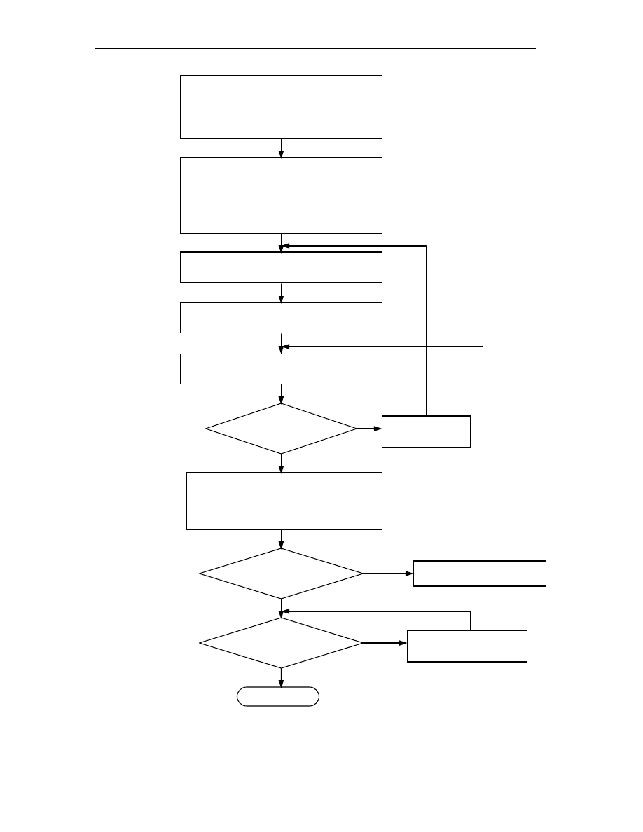
Fig.4-7 Flow Chart of EMI Filter Design
Step 2
Determine CM, IDM attenuation requirements
Step 1
Balancing noise path with enough large X cap
Measure CM and IDM noise baselines
using noise separator
dB
V
V
V
spec
CM
req
CM
3
,
+
−
=
dB
V
V
V
spec
IDM
req
IDM
6
,
+
−
=
Step 3
Choose filter topology
Step 4
Determine corner frequency
Step 5
Calculate component values
Component values
reasonable?
Yes
No
Meet spec.
for low frequency?
Tune for high frequency
performance
Step 6
Check X cap value for noise path balance.
If not large enough, redesign X cap based on
balance condition or add a cap on EUT side
End
Yes
Choose topology
of higher order
No
Meet spec.
for high frequency?
Yes
No
Lower the corner frequency

Non-Intrinsic Differential Mode Noise of Switching Power Supplies and Its Implications to Filter Design
72
4.4 Design Example
As a design example, the EMI filter for a 100 W flyback offline switching power was
design and implemented using the procedure proposed in section 4.2 to meet FCC Class
B specification. The input of the power supply is 120 V, 60 Hz single phase AC. The
output is 5 V DC. It is noted that the main objective is to meet the low-frequency specs.
Once designed and built, modification may be needed to meet the high-frequency specs.
Step1: Measure baseline EMI noise.
First without adding a filter, we measure the total noise, common-mode noise and
differential-mode noise respectively. The CM and DM noises can be obtained by using a
noise separator. The baseline IDM noise is also needed for filter design. In this example,
a 0.47
µ
F capacitor (the capacitance was calculated based on the method introduced in
Chapter 3) was connected between the phase and neutral lines and then DM noise was
measured. Because the capacitor was large enough to balance the noise paths, we can
assume the measured DM noise is the same as IDM noise.
The total noise of the power supply is shown in Fig.4-8 (a), the baseline CM and
baseline DM noises are shown in Fig.4-8 (b) and (c). Baseline IDM noise is shown in
Fig.4-8 (d).
Non-Intrinsic Differential Mode Noise of Switching Power Supplies and Its Implications to Filter Design
73
(a) Baseline Total Noise
(b) Baseline Common-Mode Noise
Total Noise
CM Noise
Non-Intrinsic Differential Mode Noise of Switching Power Supplies and Its Implications to Filter Design
74
(c) Baseline Differential-Mode Noise
(d) Baseline Intrinsic Differential-Mode Noise
Fig.4-8 Baseline Noise
DM Noise
IDM Noise
Non-Intrinsic Differential Mode Noise of Switching Power Supplies and Its Implications to Filter Design
75
Step 2 Determine the attenuation requirement
The required CM and IDM attenuation can be calculated from the equations below.
In order to cut down the labor of design work, the design procedure can be implemented
in a Mathcad spreadsheet so that the computer can do most of the calculation. It is
impossible to put the whole noise spectrum into Mathcad, so some discrete sample points
are picked to represent the whole spectrum, especially the low-frequency part. In the
example, ten sample points were taken for each noise mode.
Step 3. Choose filter topology
First, we try the simplest filter shown in Fig.4-9. In that topology, CM section is a first-
order capacitive filter and DM section is a first-order inductive filter.
Fig.4-9 First-Order Filter Topology
dB
V
V
V
spec
CM
req
CM
3
,
+
−
=
dB
V
V
V
spec
IDM
req
IDM
6
,
+
−
=
L
DM
Cy
Cy
L
G
N
L
DM
Non-Intrinsic Differential Mode Noise of Switching Power Supplies and Its Implications to Filter Design
76
Step 4. Determine filter corner frequencies
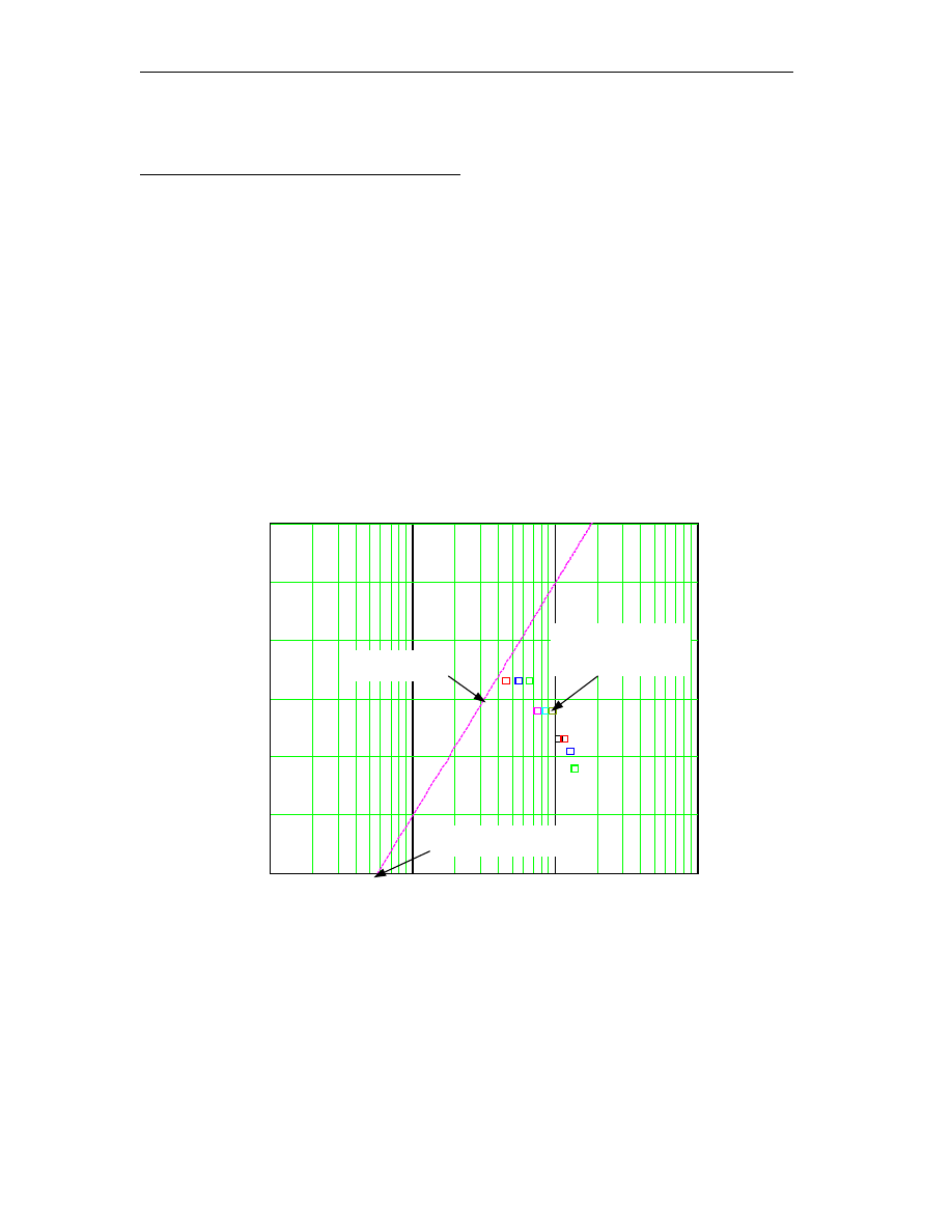
The attenuation curve of a first-order filter can be approximated to a 20dB/decade
slope when the frequency is beyond the filter corner frequency.
(a) CM Corner Frequency
1 10
3
0.01
0.1
1
10
0
10
20
30
40
50
60
Determine Corner Frequency for CM
Frequency (MHz)
CM
Attenuation
(dB)
20dB/dec
CM Attenuation
Requirement
f
R,CM=
94.4kHz
Non-Intrinsic Differential Mode Noise of Switching Power Supplies and Its Implications to Filter Design
77
(b) DM Corner Frequency
Fig.4-10 Determine Corner Frequencies of First-Order Filter
Step 5. Determine filter component values
(1) Determine CM component values
The only component in the CM section of the filter is Cy, the value of which can be
calculated:
The value of Cy is also determined by the leakage current to the ground. UL requires that
current be less than 5mA. Therefore in a 120V, 60Hz power system, the value of Cy
0.01
0.1
1
10
0
10
20
30
40
50
60
Determine Corner Frequency for IDM
Frequency (MHz)
ID
M
A
ttenuation
(dB)
IDM Attenuation
Requirement
20dB/dec
f
R,DM
=167.9kHz
nF
f
C
CM
R
y
7
.
33
50
10
4
.
94
2
1
50
2
1
3
,
=
×
×
×
=
⋅
=
π
π
Non-Intrinsic Differential Mode Noise of Switching Power Supplies and Its Implications to Filter Design
78
should be less than 4.7nF. The above calculated capacitor value is too high, which means
second-order topology should be considered.
(2) Determine DM component values
The only component in DM section of the filter is a symmetrical DM choke. The
inductance is given by:
The size of the DM choke is reasonable. Because no capacitor is used in a single inductor
DM filter, the noise paths cannot be balanced. But in this example, NIDM is dominant in
total DM noise, an X capacitor is needed. Therefore, we also should consider second-
order topology.
Now we need to repeat step 3 to step 5.
Step 3. Choose filter topology
Now we try another topology with second-order CM and second-order DM sections,
which is shown Fig.4-11.
Fig.4-11 Second-Order Filter Topology
H
f
L
DM
R
DM
µ
π
π
8
.
94
10
9
.
167
2
100
2
100
2
3
,
=
×
×
=
=
L
CM
L
DM
Cy
Cy
Cx
L
G
N
L
DM
Non-Intrinsic Differential Mode Noise of Switching Power Supplies and Its Implications to Filter Design
79
Step 4. Determine filter corner frequencies
The attenuation curve of a second-order filter can be approximated to a 40dB/decade
slope when the frequency is beyond the filter corner frequency. From Fig.4-12 (a) and
Fig.4-12 (b), we can find the corner frequency for CM section of filter is 56.2kHz and for
DM section is 100kHz.
(a) Determine Corner Frequency for CM
0.01
0.1
1
10
0
10
20
30
40
50
60
Determine Corner Frequency for CM
Frequency (MHz)
CM
Attenuation
(dB)
CM attenuation
requirement
40dB/dec
f
R,CM
=56.2kHz
Non-Intrinsic Differential Mode Noise of Switching Power Supplies and Its Implications to Filter Design
80
(b) Determine Corner Frequency for DM
Fig.4-12 Determine Corner Frequencies
Step 5. Determine filter component values
First, the values of CM components are calculated. Cy is determined by the leakage
current requirement. We choose:
L
CM
can be calculated according to (4-3)
0.01
0.1
1
10
0
10
20
30
40
50
60
Determine Corner Frequency for DM
Frequency (MHz)
DM
Attenuation
(dB)
40dB/dec
DM attenuation
requirement
f
R,DM
=100kHz
pF
C
y
4700
=
mH
L
CM
85
.
0
10
4700
2
1
10
2
.
56
2
1
12
2
3
=
×
×
⋅
×
×
=
−
π
Non-Intrinsic Differential Mode Noise of Switching Power Supplies and Its Implications to Filter Design
81
We assume the leakage inductance is 2% of the CM inductance
The actual leakage inductance can be obtained by measurement.
Then we calculate the values of DM components. As we can see, because the DM
section only deals with IDM noise, the attenuation requirement is very low. So we can
use the leakage inductance as the DM choke. We have
Then Cx can be calculated from (4-4)
We use the standard value, which is 0.15
µ
F. The final design values are given in Fig.4-26
Fig.4-13 Filter Design Values
H
L
leakage
µ
17
=
H
L
L
leakage
DM
µ
17
2
=
=
F
C
x
µ
π
148
.
0
10
17
1
10
100
2
1
6
2
3
=
×
⋅
×
×
=
−
0.85mH
17
µ
H
4700pF
4700pF
0.15
µ
F
L
G
N
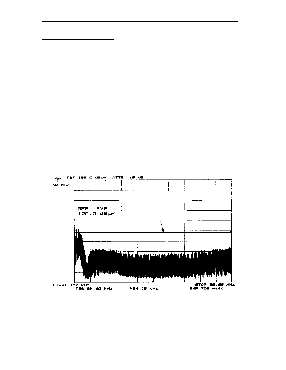
Non-Intrinsic Differential Mode Noise of Switching Power Supplies and Its Implications to Filter Design
82
Step 6. Check X capacitor value
The start frequency of FCC specs is 450kHz. The impedance of the capacitor Cx at
that frequency is given by:
The value of the capacitor is large enough to balance the noise paths.
The design is completed. The measurement results are shown in Fig.4-27. We can
see the specs have been met.
(a) CM Noise with Filter
CM Noise with Filter
FCC Class B Spec
Ω
<<
Ω
=
×
×
×
×
=
⋅
=
⋅
−
50
36
.
2
10
15
.
0
10
450
2
1
2
1
1
6
3
π
π
ω
X
X
C
f
C
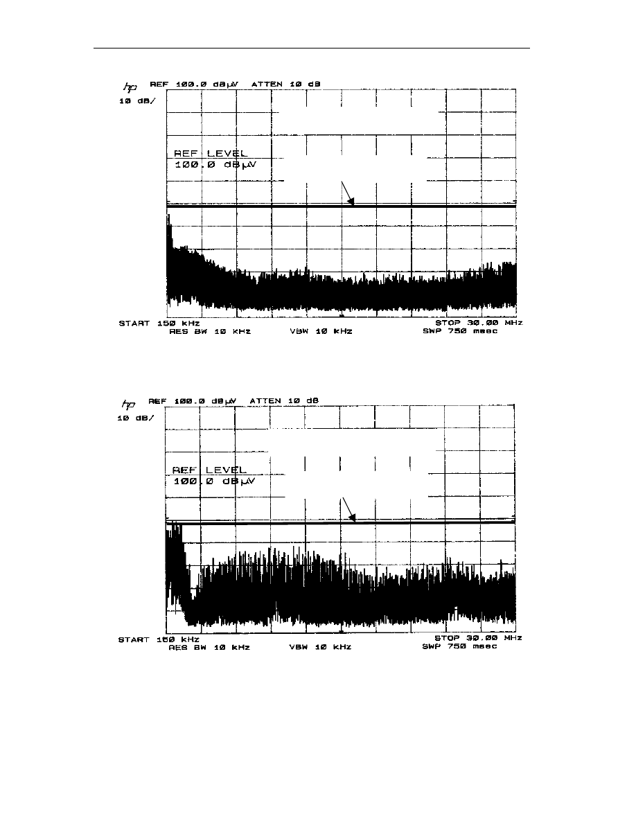
Non-Intrinsic Differential Mode Noise of Switching Power Supplies and Its Implications to Filter Design
83
(b) DM Noise with Filter
(c) Total Noise with Filter
Fig.4-14 Conducted EMI Emission with Filter
DM Noise with Filter
FCC Class B Spec.
Total Noise with Filter
FCC Class B Spec.
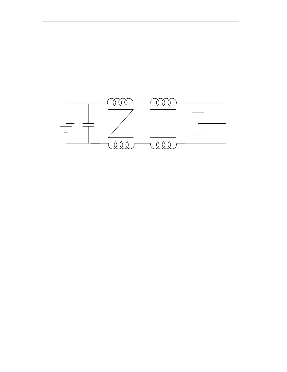
Non-Intrinsic Differential Mode Noise of Switching Power Supplies and Its Implications to Filter Design
84
To compare this design procedure with the one proposed in [3], we designed a filter
for the same power supply using the old procedure. The design result is shown in Fig.4-
15.
Fig.4-15 Design Result Using Old Procedure
The only difference is that value of
the X capacitor in both designs. A 0.82
µ
F
capacitor is used in the filter designed using old procedure. But in the filter designed
using new procedure, the capacitor is only 0.15
µ
F. The difference is caused by the noise
baseline measurement. In the new procedure, the IDM noise baseline is measured for the
design of DM section of the filter. In many cases, IDM noise baseline is much lower than
the total DM noise baseline because of the existence of NIDM. So the old design
procedure sometimes can be an over-design if NIDM noise is dominant.
0.85mH
17
µ
H
4700pF
4700pF
0.82
µ
F
L
G
N

Non-Intrinsic Differential Mode Noise of Switching Power Supplies and Its Implications to Filter Design
85
Chapter 5 Conclusions and Future Work
5.1 Conclusions
A new phenomenon, called Non-Intrinsic Differential Mode (NIDM) noise, was
investigated and discussed in the thesis. The investigation shows that NIDM noise is a
voltage-generated phenomenon. It is related to the charging and discharging of the
parasitic capacitance of the MOSFET drain and it couples through the ground path.
Therefore, NIDM noise has the nature of CM noise. That feature makes it quite different
from the conventional DM noise. But on the other hand, NIDM noise can be detected as
DM noise by using a noise separator. Now we know the DM noise is the result of
unbalanced noise paths due to the conduction states of the bridge rectifier. Because
offline switching power supplies have bridge rectifiers as input stage, the phenomenon of
NIDM is very common in this kind of power supplies. Usually the worst case of NIDM is
under high line, light load operation condition.
The best way to eliminate NIDM is to balance the noise paths with a capacitor
(known as X capacitor) connected between the phase and neutral lines. The capacitor can
make the noise current distribute evenly between two LISN branches, but it will not
suppress the noise. To reduce the amplitude of the noise, CM chokes should be used. CM
choke can effectively attenuate ground noise current, no matter it is in the form of CM or
in the form of DM. However, balancing noise paths is still necessary in tackling NIDM.

Non-Intrinsic Differential Mode Noise of Switching Power Supplies and Its Implications to Filter Design
86
If the noise currents are unbalanced, the worse case will be considered for CM choke
design, which will lead to over-design for the branch with less noise current.
The balance of noise paths depends not only on the conduction of the bridge rectifier,
but also on the arrangement of different filter components. Several cases were studied to
demonstrate the effect of filter components on NIDM. From the experimental results, we
know that symmetrical choke is always better than asymmetrical choke when NIDM is
considered. If an inductor-capacitor DM filter topology is used, placing the capacitor on
the LISN will be always helpful in eliminating NIDM. But in certain cases, when
symmetrical DM chokes or CM chokes are used, the capacitor on the EUT side can also
balance the noise paths and smaller capacitance can be used.
The above conclusions can become important guidelines for EMI filter design. A
design procedure incorporated with the concept of NIDM was proposed based on an
existing one. There are two main differences between the proposed procedure and the
existing one. One difference is in baseline EMI measurement. The IDM baseline, instead
of DM baseline, is obtained in the new procedure. Another difference is in the design of
DM filter. The filter will be designed to meet the IDM attenuation requirement. After the
IDM attenuation is met, the noise path balance condition will be checked. If the capacitor
in the filter is not large enough to balance the noise paths, some adjustments on the
capacitor value will be made or an additional capacitor will be added.

Non-Intrinsic Differential Mode Noise of Switching Power Supplies and Its Implications to Filter Design
87
5.2 Future Work
The NIDM investigation in this thesis is limited to single phase offline converters.
NIDM phenomenon also exists in three phase converters because of the input bridge
rectifier. But that issue has never been studied. The future research will focus on the
NIDM phenomenon in three phase offline converters and its implications to EMI filter
design.
In the proposed EMI filter design procedures, only first- and second-order filters are
considered. Another effort in the future research is to expand the existing procedure to
consider third- or higher order filter topologies.

Non-Intrinsic Differential Mode Noise of Switching Power Supplies and Its Implications to Filter Design
88
Reference
[1] Dongbin Zhang, Dan Y. Chen, Mark J. Nave, “Non-Intrinsic Differential Mode Noise
Caused by Ground Current in an Offline Power Supply” IEEE PESC Conference
Proceedings, Fukuoka Japan, 1998
[2] Ting Guo, Dan Y. Chen, Fred C. Lee, “Separation of Common-Mode and
Differential-Mode Conducted EMI Noise” IEEE Transactions on Power Electronics,
Vol. 11, No. 3, May 1996
[3] Fu-Yuan Shih, Dan Y. Chen, Yan-Pei Wu, Yie-Tone Chen, “A Procedure for
Designing EMI Filters for AC Line Applications” IEEE Transactions on Power
Electronics, Vol.11, No. 1, January 1996
[4] Henry W. Ott, “Noise Reduction Techniques in Electronic Systems” John Wiley &
Sons, 1988
[5] Mark J. Nave, “Power Line Filter Design for Switched-Mode Power Supplies” Van
Nostrand Reihold, 1991
[6] Hewlett Packard, “Operating and Programming Manual: 8568B Spectrum Analyzer”
Hewlett Packard Company 1984

Non-Intrinsic Differential Mode Noise of Switching Power Supplies and Its Implications to Filter Design
89
Vita: Song QU
The author was born in Tianjin, China. He obtained his BS and MS degrees from
Shanghai Jiao Tong University, Shanghai, China in 1993 and 1996 respectively, both in
Electrical Engineering.
He was hired as a Project Engineer by Shanghai Sanhuan Electric Control Corporation
from January 1996 to June 1997, designing DC and AC drive systems for various
industrial applications.
In August 1997, he enrolled at Virginia Polytechnic Institute and State University and
started pursuing another Master’s degree at Center for Power Electronic Systems
(formerly known as Virginia Power Electronics Center). His research interests at C-PES
(VPEC) include high-frequency power conversion, analysis of EMI in switching power
supplies, emission control and filter design.
Wyszukiwarka
Podobne podstrony:
Theory of Varied Consumer Choice?haviour and Its Implicati
Digital Control Of Switching Power Supply Power Factor Correction Stage
The crime of bad Power Point and how to avoid it
Magnetic Treatment of Water and its application to agriculture
The Plight of Sweatshop Workers and its Implications
Magnetic Treatment of Water and its application to agriculture
Jonathan Cook Israel and the Clash of Civilisations Iraq, Iran and the Plan to Remake the Middle E
0415471958 Routledge The Psychology of Strategic Terrorism Public and Government Responses to Attack
A review of Horizontal Well technology and its domestic application
MicroRNA Regulation of Cancer Stem Cells and Therapeutic Implications
A Comparison Of Dividend Cash Flow And Earnings Approaches To Equity Valuation
Winch The Idea of a Social Science And its Relation to Philosophy
DESIGN OF A SWITCHING MODE POWER SUPPLY WITH UPS FEATURES
SWITCHING POWER SUPPLY DESIGN CONTINUOUS MODE FLYBACK CONVERTER
(Wydruk – ATX Switching Power Supply 13,8 V Proste zmiany w celu zwiększenia napięcia wyjściowego Ja
więcej podobnych podstron