
ESP8266EX Datasheet
Version 4.3
Espressif Systems IOT Team
http://bbs.espressif.com/
Copyright
© 2015

Espressif Systems
ESP8266 Datasheet
Disclaimer and Copyright Notice
Information in this document, including URL references, is subject to change without notice.
THIS DOCUMENT IS PROVIDED "AS IS" WITH NO WARRANTIES WHATSOEVER,
INCLUDING ANY WARRANTY OF MERCHANTABILITY, NON-INFRINGEMENT, FITNESS FOR
ANY PARTICULAR PURPOSE, OR ANY WARRANTY OTHERWISE ARISING OUT OF ANY
PROPOSAL, SPECIFICATION OR SAMPLE. All liability, including liability for infringement of
any proprietary rights, relating to use of information in this document is disclaimed. No
licenses express or implied, by estoppel or otherwise, to any intellectual property rights are
granted herein.
The Wi-Fi Alliance Member Logo is a trademark of the WiFi Alliance.
All trade names, trademarks and registered trademarks mentioned in this document are
property of their respective owners, and are hereby acknowledged.
Copyright © 2015 Espressif Systems. All rights reserved.
Espressif Systems
/
June 1, 2015
2 31

Espressif Systems
ESP8266 Datasheet
1.
General Overview
6
..................................................................................................
1.1.
Introduction
6
.............................................................................................................
1.2.
Features
7
....................................................................................................................
1.3.
Parameters
7
...............................................................................................................
1.4.
Ultra Low Power Technology
9
.................................................................................
1.5.
Major Applications
9
..................................................................................................
2.
Hardware Overview
11
.............................................................................................
2.1. Pin Definitions
11
.........................................................................................................
2.2. Electrical Characteristics
13
........................................................................................
2.3.
Power Consumption
13
.............................................................................................
2.4.
Receiver Sensitivity
14
...............................................................................................
2.5.
MCU
15
........................................................................................................................
2.6.
Memory Organization
15
..........................................................................................
2.6.1. Internal SRAM and ROM
15
......................................................................................
2.6.2. External SPI Flash
15
..................................................................................................
2.7.
AHB and AHB Blocks
16
............................................................................................
3.
Pins and Definitions
17
.............................................................................................
3.1.
GPIO
17
.......................................................................................................................
3.1.1. General Purpose Input/Output Interface (GPIO)
17
.............................................
Espressif Systems
/
June 1, 2015
3 31
Table of Contents

Espressif Systems
ESP8266 Datasheet
3.2.
Secure Digital Input/Output Interface (SDIO)
18
..................................................
3.3.
Serial Peripheral Interface (SPI/HSPI)
18
.................................................................
3.3.1. General SPI (Master/Slave)
18
.................................................................................
3.3.2. SDIO / SPI (Slave)
19
.................................................................................................
3.3.3. HSPI (Master/Slave)
19
.............................................................................................
3.4.
Inter-integrated Circuit Interface (I2C)
19
...............................................................
3.5.
I2S
20
...........................................................................................................................
3.6.
Universal Asynchronous Receiver Transmitter (UART)
20
.....................................
3.7.
Pulse-Width Modulation (PWM)
21
.........................................................................
3.8.
IR Remote Control
22
................................................................................................
3.9.
ADC (Analog-to-digital Converter)
22
....................................................................
3.10. LED Light and Button
24
...........................................................................................
4.
Firmware & Software Development Kit
26
............................................................
4.1.
Features
26
..................................................................................................................
5.
Power Management
27
............................................................................................
6.
Clock Management
28
.............................................................................................
6.1.
High Frequency Clock
28
..........................................................................................
6.2.
External Reference Requirements
29
......................................................................
7.
Radio
29
......................................................................................................................
7.1.
Channel Frequencies
30
...........................................................................................
7.2.
2.4 GHz Receiver
30
..................................................................................................
7.3.
2.4 GHz Transmitter
30
..............................................................................................
Espressif Systems
/
June 1, 2015
4 31

Espressif Systems
ESP8266 Datasheet
7.4.
Clock Generator
30
....................................................................................................
8.
Appendix: QFN32 Package Size
31
.......................................................................
Espressif Systems
/
June 1, 2015
5 31
Espressif Systems
ESP8266 Datasheet
1. General Overview
1.1.
Introduction
Espressif Systems’ Smart Connectivity Platform (ESCP) is a set of high performance, high integration
wireless SOCs, designed for space and power constrained mobile platform designers. It provides
unsurpassed ability to embed WiFi capabilities within other systems, or to function as a standalone
application, with the lowest cost, and minimal space requirement.
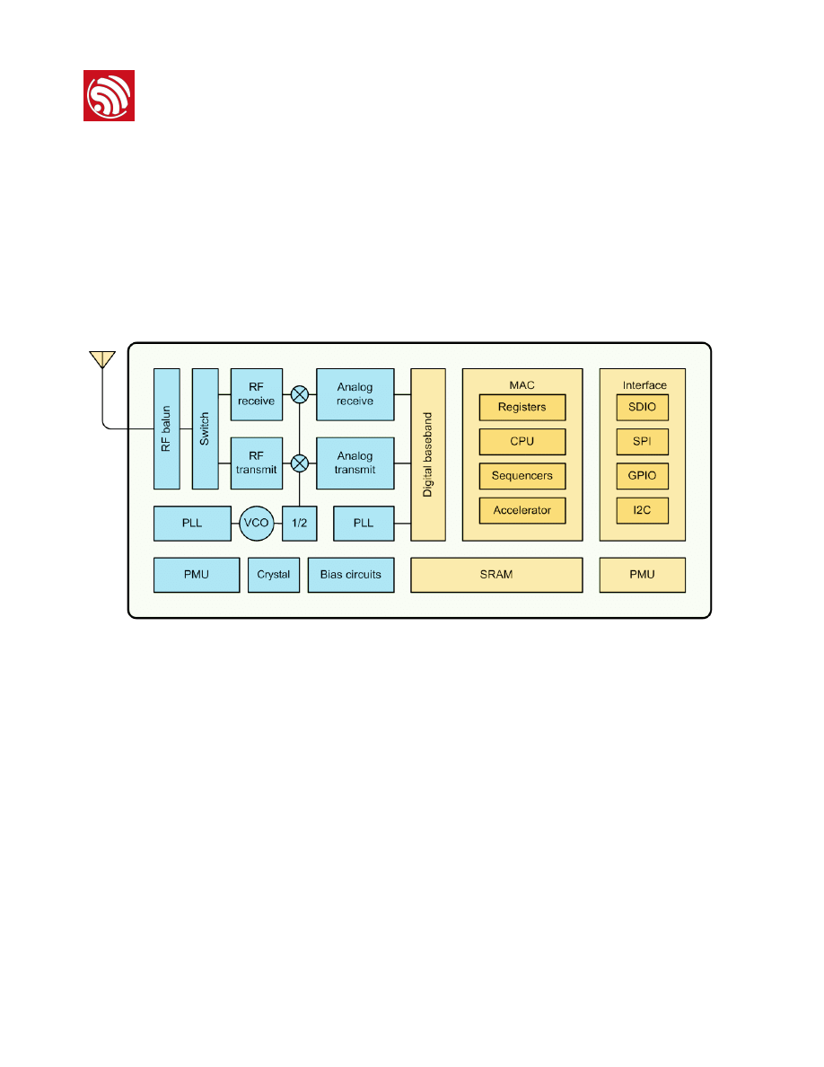
Figure 1 ESP8266EX Block Diagram
ESP8266EX offers a complete and self-contained WiFi networking solution; it can be used to host the
application or to offload WiFi networking functions from another application processor.
When ESP8266EX hosts the application, it boots up directly from an external flash. In has integrated
cache to improve the performance of the system in such applications.
Alternately, serving as a WiFi adapter, wireless internet access can be added to any micro controller-
based design with simple connectivity (SPI/SDIO or I2C/UART interface).
ESP8266EX is among the most integrated WiFi chip in the industry; it integrates the antenna
switches, RF balun, power amplifier, low noise receive amplifier, filters, power management modules,
it requires minimal external circuitry, and the entire solution, including front-end module, is designed
to occupy minimal PCB area.
ESP8266EX also integrates an enhanced version of Tensilica’s L106 Diamond series 32-bit processor,
with on-chip SRAM, besides the WiFi functionalities. ESP8266EX is often integrated with external
sensors and other application specific devices through its GPIOs; sample codes for such applications
are provided in the software development kit (SDK).
Espressif Systems
/
June 1, 2015
6 31

Espressif Systems
ESP8266 Datasheet
Espressif Systems’ Smart Connectivity Platform (ESCP) demonstrates sophisticated system-level
features include fast sleep/wake context switching for energy-efficient VoIP, adaptive radio biasing
for low-power operation, advance signal processing, and spur cancellation and radio co-existence
features for common cellular, Bluetooth, DDR, LVDS, LCD interference mitigation.
1.2.
Features
•
802.11 b/g/n
•
Integrated low power 32-bit MCU
•
Integrated 10-bit ADC
•
Integrated TCP/IP protocol stack
•
Integrated TR switch, balun, LNA, power amplifier and matching network
•
Integrated PLL, regulators, and power management units
•
Supports antenna diversity
•
WiFi 2.4 GHz, support WPA/WPA2
•
Support STA/AP/STA+AP operation modes
•
Support Smart Link Function for both Android and iOS devices
•
SDIO 2.0, (H) SPI, UART, I2C, I2S, IR Remote Control, PWM, GPIO
•
STBC, 1x1 MIMO, 2x1 MIMO
•
A-MPDU & A-MSDU aggregation & 0.4s guard interval
•
Deep sleep power <10uA, Power down leakage current < 5uA
•
Wake up and transmit packets in < 2ms
•
Standby power consumption of < 1.0mW (DTIM3)
•
+20 dBm output power in 802.11b mode
•
Operating temperature range -40C ~ 125C
•
FCC, CE, TELEC, WiFi Alliance, and SRRC certified
1.3.
Parameters
Table 1 Parameters
Espressif Systems
/
June 1, 2015
7 31

Espressif Systems
ESP8266 Datasheet
Categories
Items
Values
WiFi Paramters
Certificates
FCC/CE/TELEC/SRRC
WiFi Protocles
802.11 b/g/n
Frequency Range
2.4G-2.5G (2400M-2483.5M)
Tx Power
802.11 b: +20 dBm
802.11 g: +17 dBm
802.11 n: +14 dBm
Rx Sensitivity
802.11 b: -91 dbm (11 Mbps)
802.11 g: -75 dbm (54 Mbps)
802.11 n: -72 dbm (MCS7)
Types of Antenna
PCB Trace, External, IPEX Connector,
Ceramic Chip
Hardware
Paramaters
Peripheral Bus
UART/SDIO/SPI/I2C/I2S/IR Remote Control
GPIO/PWM
Operating Voltage
3.0~3.6V
Operating Current
Average value: 80mA
Operating Temperature Range
-40°~125°
Ambient Temperature Range
Normal temperature
Package Size
5x5mm
External Interface
N/A
Software
Parameters
WiFi mode
station/softAP/SoftAP+station
Security
WPA/WPA2
Encryption
WEP/TKIP/AES
Firmware Upgrade
UART Download / OTA (via network)
Ssoftware Development
Supports Cloud Server Development / SDK
for custom firmware development
Network Protocols
IPv4, TCP/UDP/HTTP/FTP
Espressif Systems
/
June 1, 2015
8 31

Espressif Systems
ESP8266 Datasheet
1.4.
Ultra Low Power Technology
ESP8266EX has been designed for mobile, wearable electronics and Internet of Things applications
with the aim of achieving the lowest power consumption with a combination of several proprietary
techniques. The power saving architecture operates mainly in 3 modes: active mode, sleep mode
and deep sleep mode.
By using advance power management techniques and logic to power-down functions not required
and to control switching between sleep and active modes, ESP8266EX consumes about than 60uA in
deep sleep mode (with RTC clock still running) and less than 1.0mA (DTIM=3) or less than 0.5mA
(DTIM=10) to stay connected to the access point.
When in sleep mode, only the calibrated real-time clock and watchdog remains active. The real-time
clock can be programmed to wake up the ESP8266EX at any required interval.
The ESP8266EX can be programmed to wake up when a specified condition is detected. This
minimal wake-up time feature of the ESP8266EX can be utilized by mobile device SOCs, allowing
them to remain in the low-power standby mode until WiFi is needed.
In order to satisfy the power demand of mobile and wearable electronics, ESP8266EX can be
programmed to reduce the output power of the PA to fit various application profiles, by trading off
range for power consumption.
1.5.
Major Applications
Major fields of ESP8266EX applications to Internet-of-Things include:
•
Home Appliances
•
Home Automation
•
Smart Plug and lights
•
Mesh Network
•
Industrial Wireless Control
•
Baby Monitors
•
IP Cameras
•
Sensor Networks
•
Wearable Electronics
User Configuration
AT Instruction Set, Cloud Server, Android/
iOS App
Espressif Systems
/
June 1, 2015
9 31

Espressif Systems
ESP8266 Datasheet
•
WiFi Location-aware Devices
•
Security ID Tags
•
WiFi Position System Beacons
Espressif Systems
/
June 1, 2015
10 31
Espressif Systems
ESP8266 Datasheet
2. Hardware Overview
2.1. Pin Definitions
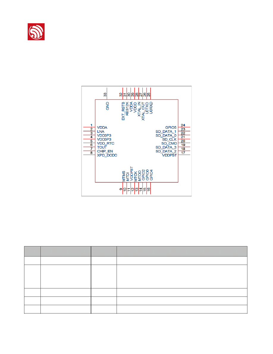
The pin assignments for 32-pin QFN package is illustrated in Fig.2.
Figure 2 Pin Assignments
Table 2 below presents an overview on the general pin attributes and the functions of each pin.
Table 2 Pin Definitions
Pin
Name
Type
Function
1
VDDA
P
Analog Power 3.0 ~3.6V
2
LNA
I/O
RF Antenna Interface. Chip Output Impedance=50Ω
No matching required but we recommend that the π-type
matching network is retained.
3
VDD3P3
P
Amplifier Power 3.0~3.6V
4
VDD3P3
P
Amplifier Power 3.0~3.6V
5
VDD_RTC
P
NC (1.1V)
Espressif Systems
/
June 1, 2015
11 31

Espressif Systems
ESP8266 Datasheet
6
TOUT
I
ADC Pin (note: an internal pin of the chip) can be used to
check the power voltage of VDD3P3 (Pin 3 and Pin4) or the
input voltage of TOUT (Pin 6). These two functions cannot be
used simultaneously.
7
CHIP_EN
I
Chip Enable.
High: On, chip works properly; Low: Off, small current
8
XPD_DCDC
I/O
Deep-Sleep Wakeup;GPIO16
9
MTMS
I/O
GPIO14; HSPI_CLK
10
MTDI
I/O
GPIO12; HSPI_MISO
11
VDDPST
P
Digital/IO Power Supply (1.8V~3.3V)
12
MTCK
I/O
GPIO13; HSPI_MOSI; UART0_CTS
13
MTDO
I/O
GPIO15; HSPI_CS; UART0_RTS
14
GPIO2
I/O
UART Tx during flash programming; GPIO2
15
GPIO0
I/O
GPIO0; SPI_CS2
16
GPIO4
I/O
GPIO4
17
VDDPST
P
Digital/IO Power Supply (1.8V~3.3V)
18
SDIO_DATA_2
I/O
Connect to SD_D2 (Series R: 200Ω); SPIHD; HSPIHD; GPIO9
19
SDIO_DATA_3
I/O
Connect to SD_D3 (Series R: 200Ω); SPIWP; HSPIWP; GPIO10
20
SDIO_CMD
I/O
Connect to SD_CMD (Series R: 200Ω); SPI_CS0; GPIO11
21
SDIO_CLK
I/O
Connect to SD_CLK (Series R: 200Ω); SPI_CLK; GPIO6
22
SDIO_DATA_0
I/O
Connect to SD_D0 (Series R: 200Ω); SPI_MSIO; GPIO7
23
SDIO_DATA_1
I/O
Connect to SD_D1 (Series R: 200Ω); SPI_MOSI; GPIO8
24
GPIO5
I/O
GPIO5
25
U0RXD
I/O
UART Rx during flash programming; GPIO3
26
U0TXD
I/O
UART Tx during flash progamming; GPIO1; SPI_CS1
27
XTAL_OUT
I/O
Connect to crystal oscillator output, can be used to provide BT
clock input
28
XTAL_IN
I/O
Connect to crystal oscillator input
29
VDDD
P
Analog Power 3.0V~3.6V
30
VDDA
P
Analog Power 3.0V~3.6V
31
RES12K
I
Serial connection with a 12 kΩ resistor and connect to the
ground
32
EXT_RSTB
I
External reset signal (Low voltage level: Active)
Espressif Systems
/
June 1, 2015
12 31
Espressif Systems
ESP8266 Datasheet
Note: GPIO2, GPIO0, MTDO can be configurable as 3-bit SDIO mode.
2.2. Electrical Characteristics
Table 3 ESP8266EX Electrical Characteristics
2.3.
Power Consumption
The following current consumption is based on 3.3V supply, and 25°C ambient, using internal
regulators. Measurements are done at antenna port without SAW filter. All the transmitter’s
measurements are based on 90% duty cycle, continuous transmit mode.
Table 4 Description on Power Consumption
Parameters
Conditions
Min
Typical
Max
Unit
Storage Temperature Range
-40
Normal
125
℃
Maximum Soldering Temperature
IPC/JEDEC J-
STD-020
260
℃
Working Voltage Value
3.0
3.3
3.6
V
I/O
V
IL
/V
IH
-0.3/0.75V
IO
0.25V
IO
/3.6
V
V
OL
/V
OH
N/0.8V
IO
0.1V
IO
/N
I
MAX
12
mA
Electrostatic Discharge (HBM)
TAMB=25℃
2
KV
Electrostatic Discharge (CDM)
TAMB=25℃
0.5
KV
Parameters
Min
Typical
Max
Unit
Tx802.11b, CCK 11Mbps, P OUT=+17dBm
170
mA
Tx 802.11g, OFDM 54Mbps, P OUT =+15dBm
140
mA
Tx 802.11n, MCS7, P OUT =+13dBm
120
mA
Rx 802.11b, 1024 bytes packet length , -80dBm
50
mA
Rx 802.11g, 1024 bytes packet length, -70dBm
56
mA
Rx 802.11n, 1024 bytes packet length, -65dBm
56
mA
Modem-Sleep①
15
mA
Light-Sleep②
0.9
mA
Deep-Sleep③
10
uA
Power Off
0.5
uA
Espressif Systems
/
June 1, 2015
13 31

Espressif Systems
ESP8266 Datasheet
①
: Modem-Sleep requires the CPU to be working, as in PWM or I2S applications. According to
802.11 standards (like U-APSD), it saves power to shut down the WiFi Modem circuit while
maintaining a WiFi connection with no data transmission. E.g. in DTIM3, to maintain a sleep 300ms-
wake 3ms cycle to receive AP’s Beacon packages, the current is about 15mA
②
: During Light-Sleep, the CPU may be suspended in applications like WiFi switch. Without data
transmission, the WiFi Modem circuit can be turned off and CPU suspended to save power
according to the 802.11 standard (U-APSD). E.g. in DTIM3, to maintain a sleep 300ms-wake 3ms
cycle to receive AP’s Beacon packages, the current is about 0.9mA.
③
: Deep-Sleep does not require WiFi connection to be maintained. For application with long time
lags between data transmission, e.g. a temperature sensor that checks the temperature every 100s,
sleep 300s and waking up to connect to the AP (taking about 0.3~1s), the overall average current is
less than 1mA.
2.4.
Receiver Sensitivity
The following are measured under room temperature conditions with 3.3V and 1.1V power supplies.
Table 5 Receiver Sensitivity
Parameters
Min
Typical
Max
Unit
Input frequency
2412
2484
MHz
Input impedance
50
Ω
Input reflection
-10
dB
Output power of PA for 72.2Mbps
15.5
16.5
17.5
dBm
Output power of PA for 11b mode
19.5
20.5
21.5
dBm
Sensitivity
DSSS, 1Mbps
-98
dBm
CCK, 11Mbps
-91
dBm
6Mbps (1/2 BPSK)
-93
dBm
54Mbps (3/4 64-QAM)
-75
dBm
HT20, MCS7 (65Mbps, 72.2Mbps)
-72
dBm
Adjacent Channel Rejection
OFDM, 6Mbps
37
dB
OFDM, 54Mbps
21
dB
HT20, MCS0
37
dB
HT20, MCS7
20
dB
Espressif Systems
/
June 1, 2015
14 31

Espressif Systems
ESP8266 Datasheet
2.5.
MCU
ESP8266EX is embedded with Tensilica L106 32-bit micro controller (MCU), which features extra low
power consumption and 16-bit RSIC. The CPU clock speed is 80MHz. It can also reach a maximum
value of 160MHz. Real Time Operation System (RTOS) is enabled. Currently, only 20% of MIPS has
been occupied by the WiFi stack, the rest can all be used for user application programming and
development. The following interfaces can be used to connect to the MCU embedded in
ESP8266EX:
•
Programmable RAM/ROM interfaces (iBus), which can be connected with memory controller,
and can also be used to visit external flash;
•
Data RAM interface (dBus), which can connected with memory controller;
•
AHB interface, can be used to visit the register.
2.6.
Memory Organization
2.6.1.
Internal SRAM and ROM
ESP8266EX WiFi SoC is embedded with memory controller, including SRAM and ROM. MCU can visit
the memory units through iBus, dBus, and AHB interfaces. All memory units can be visited upon
request, while a memory arbiter will decide the running sequence according to the time when these
requests are received by the processor.
According to our current version of SDK provided, SRAM space that is available to users is assigned
as below:
• RAM size < 36kB, that is to say, when ESP8266EX is working under the station mode and is
connected to the router, programmable space accessible to user in heap and data section is
around 36kB.)
• There is no programmable ROM in the SoC, therefore, user program must be stored in an
external SPI flash.
2.6.2.
External SPI Flash
An external SPI flash is used together with ESP8266EX to store user programs. Theoretically
speaking, up to 16 Mbyte memory capacity can be supported.
Suggested SPI Flash memory capacity:
• OTA is disabled: the minimum flash memory that can be supported is 512 kByte;
• OTA is enabled: the minimum flash memory that can be supported is 1 Mbyte.
Several SPI modes can be supported, including Standard SPI, Dual SPI, DIO SPI, QIO SPI, and Quad
SPI.
Espressif Systems
/
June 1, 2015
15 31

Espressif Systems
ESP8266 Datasheet
Therefore, please choose the correct SPI mode when you are downloading into the flash, otherwise
firmwares/programs that you downloaded may not work in the right way.
2.7.
AHB and AHB Blocks
The AHB blocks performs the function of an arbiter, controls the AHB interfaces from the MAC, SDIO
(host) and CPU. Depending on the address, the AHB data requests can go into one of the two slaves:
APB block, or
flash controller (usually for standalone applications).
Data requests to the memory controller are usually high speed requests, and requests to the APB
block are usually register access.
The APB block acts as a decoder. It is meant only for access to programmable registers within
ESP8266’s main blocks. Depending on the address, the APB request can go to the radio, SI/SPI, SDIO
(host), GPIO, UART, real-time clock (RTC), MAC or digital baseband.
Espressif Systems
/
June 1, 2015
16 31
Espressif Systems
ESP8266 Datasheet
3. Pins and Definitions
The chipset encapsulates variable analog and data transmission I/Os, descriptions and definitions of
which are explained below in detail.
3.1.
GPIO
3.1.1.
General Purpose Input/Output Interface (GPIO)
There are up to 17 GPIO pins. They can be assigned to various functions by the firmware. Each GPIO
can be configured with internal pull-up (except XPD_DCDC, which is configured with internal pull-
down), input available for sampling by a software register, input triggering an edge or level CPU
interrupt, input triggering a level wakeup interrupt, open-drain or push-pull output driver, or output
source from a software register, or a sigma-delta PWM DAC.
These pins are multiplexed with other functions such as I2C, I2S, UART, PWM, IR Remote Control, etc.
Data I/O soldering pad is bidirectional and tri-state that include data input and output controlling
buffer. Besides, I/O can be set as a specific state and remains like this. For example, if you intend to
lower the power consumption of the chip, all data input and output enable signals can be set as
remaining low power state. You can transport some specific state into the I/O. When the I/O is not
powered by external circuits, the I/O will remain to be the state that it was used the last time. Some
positive feedback is generated by the state-remaining function of the pins, therefore, if the external
driving power must be stronger than the positive feedback. Even so, the driving power that is
needed is within 5uA.
Table 6 Pin Definitions of GPIOs
All digital IO pins are protected from over-voltage with a snap-back circuit connected between the
pad and ground. The snap back voltage is typically about 6V, and the holding voltage is 5.8V. This
Variables
Symbol
Min
Max
Unit
Input Low Voltage
V
IL
-0.3
0.25×V
IO
V
Input High Voltage
V
IH
0.75×V
IO
3.3
V
Input Leakage Current
I
IL
50
nA
Output Low Voltage
V
OL
0.1×V
IO
V
Output High Voltage
V
OH
0.8×V
IO
V
Input Pin Resistance Value
C
pad
2
pF
VDDIO
V
IO
1.8
3.3
V
Maximum Driving Power
I
MAX
12
mA
Temerpature
T
amb
-40
125
°C
Espressif Systems
/
June 1, 2015
17 31
Espressif Systems
ESP8266 Datasheet
provides protection from over-voltages and ESD. The output devices are also protected from
reversed voltages with diodes.
3.2.
Secure Digital Input/Output Interface (SDIO)
One Slave SDIO has been defined by ESP8266EX, the definitions of which are described in Table 7
below. 4bit 25MHz SDIO v1.1 and 4bit 50MHz SDIO v2.0 are supported.
Table 7 Pin Definitions of SDIOs
3.3.
Serial Peripheral Interface (SPI/HSPI)
Currently, one general Slave/Master SPI, one Slave SDID/SPI, and one general Slave/Master HSPI
have been defined by ESP8266EX. Functions of all these pins can be implemented via hardware. The
pin definitions are are described below:
3.3.1.
General SPI (Master/Slave)
Table 8
Pin Definitions of General SPIs
Pin Name
Pin Num
IO
Function Name
SDIO_CLK
21
IO6
SDIO_CLK
SDIO_DATA0
22
IO7
SDIO_DATA0
SDIO_DATA1
23
IO8
SDIO_DATA1
SDIO_DATA_2
18
IO9
SDIO_DATA_2
SDIO_DATA_3
19
IO10
SDIO_DATA_3
SDIO_CMD
20
IO11
SDIO_CMD
Pin Name
Pin Num
IO
Function Name
SDIO_CLK
21
IO6
SPICLK
SDIO_DATA0
22
IO7
SPIQ/MISO
SDIO_DATA1
23
IO8
SPID/MOSI
SDIO_DATA_2
18
IO9
SPIHD
SDIO_DATA_3
19
IO10
SPIWP
SDIO_CMD
20
IO11
SPICS0
U0TXD
26
IO1
SPICS1
GPIO0
15
IO0
SPICS2
Espressif Systems
/
June 1, 2015
18 31
Espressif Systems
ESP8266 Datasheet
3.3.2.
SDIO / SPI (Slave)
Table
9 Pin Definitions of SDIO / SPI (Slave)
3.3.3.
HSPI (Master/Slave)
Table
10 Pin Definitions of HSPI (Master/Slave)
Note:
•
SPI mode can be implemented via software programming. The clock frequency can reach up to
a maximum value of 80MHz.
•
Function of Slave SDIO/SPI interface can be implemented via hardware, and linked list DMA
(Direct Memory Access) is supported, software overheads are smaller. However, there is no
linked list DMA on general SPI and HSPI, and the software overheads are larger, therefore, the
data transmitting speed will be restrained by software processing speed.
3.4.
Inter-integrated Circuit Interface (I2C)
One I2C, which is mainly used to connect with micro controller and other peripheral equipment such
as sensors, is defined by ESP8266EX. The present pin definition of I2C is as defined below:
Pin Name
Pin Num
IO
Function Name
SDIO_CLK
21
IO6
SPI_SLAVE_CLK
SDIO_DATA0
22
IO7
SPI_SLAVE_MISO
SDIO_DATA1
23
IO8
SPI_SLAVE_INT
SDIO_DATA_2
18
IO9
NC
SDIO_DATA_3
19
IO10
SPI_SLAVE_CS
SDIO_CMD
20
IO11
SPI_SLAVE_MOSI
Pin Name
Pin Num
IO
Function Name
MTMS
9
IO14
HSPICLK
MTDI
10
IO12
HSPIQ/MISO
MTCK
12
IO13
HSPID/MOSI
MTDO
13
IO15
HPSICS
Espressif Systems
/
June 1, 2015
19 31
Espressif Systems
ESP8266 Datasheet
Table 11 Pin Definitions of I2C
Both I2C-Master and I2C-Slave are supported. I2C interface functionality can be realized via software
programming, the clock frequency can be up to around 100KHz at most. It should be noted that I2C
clock frequency should be higher than the slowest clock frequency of the slave device.
3.5.
I2S
Currently one I2S data input interface and one I2S data output interface are defined. I2S interface is
mainly used in applications such as data collection, processing, and transmission of audio data, as
well as the input and output of serial data. For example, LED lights (WS2812 series) are supported.
The pin definition of I2S is as defined below:
Table 12 Pin Definitions of I2S
I2S functionality can be realized via software programming, the GPIOs that will be used are
multiplexed, and linked list DMA is supported.
3.6.
Universal Asynchronous Receiver Transmitter (UART)
Two UART interfaces, UART0 and UART1, have been defined by ESP8266EX, the definitions are as
below:
Pin Name
Pin Num
IO
Function Name
MTMS
9
IO14
I2C_SCL
GPIO2
14
IO2
I2C_SDA
I2S Data Input:
Pin Name
Pin Num
IO
Function Name
MTDI
10
IO12
I2SI_DATA
MTCK
12
IO13
I2SI_BCK
MTMS
9
IO14
I2SI_WS
I2S Data Output:
Pin Name
Pin Num
IO
Function Name
MTDO
13
IO15
I2SO_BCK
U0RXD
25
IO3
I2SO_DATA
GPIO2
14
IO2
I2SO_WS
Espressif Systems
/
June 1, 2015
20 31
Espressif Systems
ESP8266 Datasheet
Table 13 Pin Definitions of UART Interfaces
Data transfers to/from UART interfaces can be implemented via hardware. The data transmission
speed via UART interfaces can reach 115200*40 (4.5Mbps).
UART0 can be for communication. It supports fluid control. Since UART1 features only data transmit
signal (Tx), it is usually used for printing log.
Notes: By default, UART0 will output some printed information when the device is powered on and is
booting up. The baud rate of the printed information is closely related to the frequency of the
external crystal oscillator. If the frequency of the crystal oscillator is 40MHz, then the baud rate for
printing is 115200; if the frequency of the crystal oscillator is 26MHz, then the baud rate for printing
is 74880. If the printed information exerts any influence on the functionality of your device, you’d
better block the printing during the power-on period by changing (
U0TXD,U0RXD
) to (
MTDO,MTCK
).
3.7.
Pulse-Width Modulation (PWM)
Four PWM output interfaces have been defined by ESP8266EX. They can be extended by users
themselves. The present pin definitions of the PWM interfaces are defined as below:
Table 14 Pin Definitions of PWM Interfaces
The functionality of PWM interfaces can be implemented via software programming. For example, in
the LED smart light demo, the function of PWM is realized by interruption of the timer, the minimum
resolution can reach as much as 44 ns. PWM frequency range is adjustable from 1000 us to 10000 us,
Pin Type
Pin Name
Pin Num
IO
Function Name
UART0
U0RXD
25
IO3
U0RXD
U0TXD
26
IO1
U0TXD
MTDO
13
IO15
U0RTS
MTCK
12
IO13
U0CTS
UART1
GPIO2
14
IO2
U1TXD
SD_D1
23
IO8
U1RXD
Pin Name
Pin Num
IO
Function Name
MTDI
10
IO12
PWM0
MTDO
13
IO15
PWM1
MTMS
9
IO14
PWM2
GPIO4
16
IO4
PWM3
Espressif Systems
/
June 1, 2015
21 31
Espressif Systems
ESP8266 Datasheet
i.e., between 100Hz and 1KHz. When the PWM frequency is at 1 KHz, the duty ratio will reach
1/22727, and over 14 bit resolution will be achieved at 1KHz refresh rate.
3.8.
IR Remote Control
Currently, only one Infrared remote control interface is defined, the pin definition is as below:
Table 14 Pin Definition of IR Remote Control
The functionality of Infrared remote control interface can be implemented via software
programming. NEC coding, modulation, and demodulation are used by this interface. The frequency
of modulated carrier signal is 38KHz, while the duty ratio of the square wave is 1/3. The length of
data transmission, which is around 1m, is determined by two factors: one is the maximum value of
rated current, the other is internal current-limiting resistance value in the infrared receiver. The larger
the resistance value, the lower the current, so is the power, and vice versa. The transmission angle is
between 15° and 30°, and is mainly determined by the radiation direction of the infrared receiver.
Notes: Among the eight interfaces mentioned above, most of them can be multiplexed. Pin
definitions that can be defined is not limited to the eight ones herein mentioned, customers can self
customise the functions of the pins according to their specific application scenarios. Functions of
these pins can be implemented via software programming and hardware.
3.9.
ADC (Analog-to-digital Converter)
ESP8266EX is embedded with a 10-bit precision SARADC. Currently, TOUT (Pin6) is defined as ADC
interface, the definition of which is described below:
Table 16 Pin Definition of ADC
The following two applications can be implemented using ADC (Pin6). However, these two
applications cannot be implemented concurrently.
• Test the power supply voltage of VDD3P3 (Pin 3 and Pin 4).
The function used to test the power supply voltage on PA_VDD pin is:
uint16
system_get_vdd33(void)
• Test the input voltage of TOUT (Pin 6):
Pin Name
Pin Num
IO
Function Name
MTMS
9
IO12
IR Tx
GPIO5
24
IO5
IR Rx
Pin Name
Pin Num
Function Name
TOUT
6
ADC Interface
Espressif Systems
/
June 1, 2015
22 31

Espressif Systems
ESP8266 Datasheet
The function used to test the input voltage of TOUT is:
uint16 system_adc_read(void)
RF-init
parameter in the following passage refers to
esp_init_data_default.bin
Note One:
In
RF_init
parameter
esp_init_data_default.bin
(0 - 127 byte), the 107th byte is defined as
“vdd33_const“. Definitions of “vdd33_const“ is described below:
(1)If vdd33_const = 0xff, the power voltage of Pin 3 and Pin 4 will be tested by the internal self-
calibration process of ESP8266EX chipset itself. RF circuit conditions should be optimized according
to the testing results.
Application One:
Test the power supply voltage of VDD3P3 (Pin 3 and Pin 4).
Hardware Design:
TOUT must be dangled.
RF-init
Parameter: The 107th byte of
esp_init_data_default.bin
(0 - 127 byte),
“vdd33_const“, must set to be 0xFF, i.e., the value of “vdd33_const“ is 255.
RF Calibration
Process:
Optimize the RF circuit conditions based on the testing results of VDD3P3 (Pin 3
and Pin 4).
User Programming:
Use
system_get_vdd33
instead of
system_adc_read
.
Application Two:
Test the input voltage of TOUT (Pin 6).
Hardware Design:
The input voltage range is 0 to 1.0 V when TOUT is connected to external
circuit.
RF-init
Parameter: The value of the 107th byte of
esp_init_data_default.bin
(0 - 127
byte), “vdd33_const“, must be set to be the real power supply voltage of Pin
3 and Pin 4.
The working power voltage range of ESP8266EX is between 1.8V and 3.6V,
while the unit of “vdd33_const“ is 0.1V, therefore, the effective value range
of “vdd33_const“ is 18 to 36.
RF Calibration
Process:
Optimize the RF circuit conditions based on the value of “vdd33_const“.
The permissible error is ±0.2V.
User Programming:
Use
system_adc_read
instead of
system_get_vdd33
.
Espressif Systems
/
June 1, 2015
23 31

Espressif Systems
ESP8266 Datasheet
(2)If 18 =< vdd33_const =< 36, ESP8266EX RF Calibration and optimization process is
implemented via (vdd33_const/10).
(3)If vdd33_const < 18 or 36 < vdd33_const < 255, ESP8266EX RF Calibration and optimization
process is implemented via the default value 3.0V.
Note Two:
Function
system_get_vdd33
is used to test the power supply voltage of VDD3P3 (Pin 3 and Pin 4).
Details on this function are described below:
(1)Pin Tout must be dangled. The 107th byte of
esp_init_data_default.bin
(0 - 127 byte),
“vdd33_const“, must set to be 0xFF.
(2)If the 107th byte of
esp_init_data_default.bin
(0 - 127 byte), “vdd33_const“, is equal to
0xff
, the returned value of function
system_get_vdd33
will be an effective value, otherwise
0xffff
will be returned.
(3)The unit of the returned value is: 1/1024 V.
Note Three:
Function system_adc_read is defined to test the input voltage of Pin TOUT (Pin 6). Details on this
function are described below:
(1)The value of the 107th byte of
esp_init_data_default.bin
(0 - 127 byte), “vdd33_const“,
must be set to be the real power supply voltage of Pin 3 and Pin 4.
(2)If the 107th byte of
esp_init_data_default.bin
(0 - 127 byte), “vdd33_const“, is NOT
equal to
0xff
, the returned value of
system_adc_read
will be an effective value of the input voltage
of Pin TOUT, otherwise
0xffff
will be returned.
(3)The unit of the returned value is: 1/1024 V.
3.10. LED Light and Button
ESP8266EX features up to 17 GPIOs, all of which can be assigned to realise various functions of LED
lights and buttons. Definitions of some GPIOs that are assigned with certain functions in our demo
application design are shown below:
Table 17 Pin Definitions of LED and Button
Pin Name
Pin Num
IO
Function Name
MTCK
12
IO13
Button (Reset)
GPIO0
15
IO0
WiFi Light
MTDI
10
IO12
Link Light
Espressif Systems
/
June 1, 2015
24 31

Espressif Systems
ESP8266 Datasheet
Altogether three interfaces have been defined, one is for the button, and the other two is for LED
light. Generally, MTCK is used to control the reset button, GPIO0 is used as an signal to indicate the
WiFi working state, MTDI is used as a signal light to indicate communication between the device and
the server.
Note: Among the nine interfaces mentioned above, most of them can be multiplexed. Pin
definitions that can be defined is not limited to the eight ones herein mentioned,
customers can self customise the functions of the pins according to their specific
application scenarios. Functions of these pins can be implemented via software
programming and hardware.
Espressif Systems
/
June 1, 2015
25 31

Espressif Systems
ESP8266 Datasheet
4. Firmware & Software Development Kit
The application and firmware is executed in on-chip ROM and SRAM, which loads the instructions
during wake-up, through the SDIO interface, from the external flash.
The firmware implements TCP/IP, the full 802.11 b/g/n/e/i WLAN MAC protocol and WiFi Direct
specification. It supports not only basic service set (BSS) operations under the distributed control
function (DCF) but also P2P group operation compliant with the latest WiFi P2P protocol. Low level
protocol functions are handled automatically by ESP8266:
•
RTS/CTS
•
acknowledgement
•
fragmentation and defragmentation
•
aggregation
•
frame encapsulation (802.11h/RFC 1042)
•
automatic beacon monitoring / scanning, and
•
P2P WiFi direct
Passive or active scanning, as well as P2P discovery procedure is performed autonomously once
initiated by the appropriate command. Power management is handled with minimum host
interaction to minimize active duty period.
4.1.
Features
The SDK includes the following library functions:
•
802.11 b/g/n/d/e/i/k/r support;
•
WiFi Direct (P2P) support:
•
P2P Discovery, P2P Group Owner mode, P2P Power Management
•
Infrastructure BSS Station mode / P2P mode / softAP mode support;
•
Hardware accelerators for CCMP (CBC-MAC, counter mode), TKIP (MIC, RC4), WAPI (SMS4),
WEP (RC4), CRC;
•
WPA/WPA2 PSK, and WPS driver;
•
Additional 802.11i security features such as pre-authentication, and TSN;
•
Open Interface for various upper layer authentication schemes over EAP such as TLS, PEAP,
LEAP, SIM, AKA, or customer specific;
•
802.11n support (2.4GHz);
•
Supports MIMO 1×1 and 2×1, STBC, A-MPDU and A-MSDU aggregation and 0.4μs guard
interval;
Espressif Systems
/
June 1, 2015
26 31

Espressif Systems
ESP8266 Datasheet
•
WMM power save U-APSD;
•
Multiple queue management to fully utilize traffic prioritization defined by 802.11e standard;
•
UMA compliant and certified;
•
802.1h/RFC1042 frame encapsulation;
•
Scattered DMA for optimal CPU off load on Zero Copy data transfer operations;
•
Antenna diversity and selection (software managed hardware);
•
Clock/power gating combined with 802.11-compliant power management dynamically adapted
to current connection condition providing minimal power consumption;
•
Adaptive rate fallback algorithm sets the optimum transmission rate and Tx power based on
actual SNR and packet loss information;
•
Automatic retransmission and response on MAC to avoid packet discarding on slow host
environment;
•
Seamless roaming support;
•
Configurable packet traffic arbitration (PTA) with dedicated slave processor based design
provides flexible and exact timing Bluetooth co-existence support for a wide range of Bluetooth
Chip vendors;
•
Dual and single antenna Bluetooth co-existence support with optional simultaneous receive
(WiFi/Bluetooth) capability.
5. Power Management
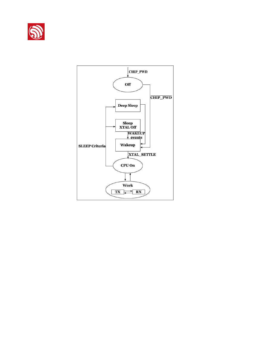
The chip can be put into the following states:
•
OFF: CHIP_PD pin is low. The RTC is disabled. All registers are cleared.
•
DEEP_SLEEP: Only RTC is powered on – the rest of the chip is powered off. Recovery memory
of RTC can keep basic WiFi connecting information.
•
SLEEP: Only the RTC is operating. The crystal oscillator is disabled. Any wakeup events (MAC,
host, RTC timer, external interrupts) will put the chip into the WAKEUP state.
•
WAKEUP: In this state, the system goes from the sleep states to the PWR state. The crystal
oscillator and PLLs are enabled.
•
ON: the high speed clock is operational and sent to each block enabled by the clock control
register. Lower level clock gating is implemented at the block level, including the CPU, which
can be gated off using the WAITI instruction, while the system is on.
Espressif Systems
/
June 1, 2015
27 31
Espressif Systems
ESP8266 Datasheet
Figure 3 Illustration of Power Management
6. Clock Management
6.1.
High Frequency Clock
The high frequency clock on ESP8266EX is used to drive both transmit and receive mixers. This clock
is generated from the internal crystal oscillator and an external crystal. The crystal frequency can
range from 26MHz to 52MHz.
While internal calibration of the crystal oscillator ensures that a wide range of crystals can be used, in
general, the quality of the crystal is still a factor to consider, to have reasonable phase noise that is
required for good performance. When the crystal selected is sub-optimal due to large frequency
drifts or poor Q-factor, the maximum throughput and sensitivity of the WiFi system is degraded.
Please refer to the application notes on how the frequency offset can be measured.
Espressif Systems
/
June 1, 2015
28 31
Espressif Systems
ESP8266 Datasheet
Table 18 High Frequency Clock
6.2.
External Reference Requirements
For an externally generated clock, the frequency can range from 26MHz to 52MHz can be used. For
good performance of the radio, the following characteristics are expected of the clock:
Table 19 External Clock Reference
7. Radio
The ESP8266EX radio consists of the following main blocks:
•
2.4GHz receiver
•
2.4GHz transmitter
•
High speed clock generators and crystal oscillator
•
Real time clock
•
Bias and regulators
•
Power management
Parameter
Symbol
Min
Max
Unit
Frequency
FXO
26
52
MHz
Loading capacitance
CL
32
pF
Motional capacitance
CM
2
5
pF
Series resistance
RS
0
65
Ω
Frequency tolerance
ΔFXO
-15
15
ppm
Frequency vs temperature (-25°C ~
75°C)
ΔFXO,Temp
-15
15
ppm
Parameter
Symbol
Min
Max
Unit
Clock amplitude
VXO
0.2
1
Vpp
External clock accuracy
ΔFXO,EXT
-15
15
ppm
Phase noise @1kHz offset, 40MHz clock
-120
dBc/Hz
Phase noise @10kHz offset, 40MHz clock
-130
dBc/Hz
Phase noise @100kHz offset, 40MHz clock
-138
dBc/Hz
Espressif Systems
/
June 1, 2015
29 31

Espressif Systems
ESP8266 Datasheet
7.1.
Channel Frequencies
The RF transceiver supports the following channels according to the IEEE802.11b/g/n standards.
Table 20 Frequency Channel
7.2.
2.4 GHz Receiver
The 2.4GHz receiver downconverts the RF signal to quadrature baseband signals and converts them
to the digital domain with 2 high resolution high speed ADCs. To adapt to varying signal channel
conditions, RF filters, automatic gain control (AGC), DC offset cancelation circuits and baseband
filters are integrated within ESP8266EX.
7.3.
2.4 GHz Transmitter
The 2.4GHz transmitter up-converts the quadrature baseband signals to 2.4GHz, and drives the
antenna with a high powered CMOS power amplifier. The use of digital calibration further improves
the linearity of the power amplifier, enabling a state of art performance of delivering +19.5dBm
average power for 802.11b transmission and +16dBm for 802.11n transmission.
Additional calibrations are integrated to cancel any imperfections of the radio, such as:
▪
carrier leakage,
▪
I/Q phase matching, and
▪
baseband nonlinearities
This reduces the amount of time required and test equipment required for production testing.
7.4.
Clock Generator
The clock generator generates quadrature 2.4 GHz clock signals for the receiver and transmitter. All
components of the clock generator are integrated on-chip, including:
Channel No
Frequency (MHz)
Channel No
Frequency (MHz)
1
2412
8
2447
2
2417
9
2452
3
2422
10
2457
4
2427
11
2462
5
2432
12
2467
6
2437
13
2472
7
2442
14
2484
Espressif Systems
/
June 1, 2015
30 31
Espressif Systems
ESP8266 Datasheet
▪
inductor,
▪
varactor, and
▪
loop filter
The clock generator has built-in calibration and self test circuits. Quadrature clock phases and phase
noise are optimized on-chip with patented calibration algorithms to ensure the best receiver and
transmitter performance.
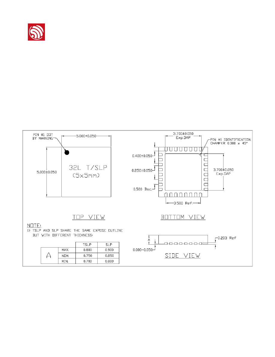
8. Appendix: QFN32 Package Size
Espressif Systems
/
June 1, 2015
31 31
Wyszukiwarka
Podobne podstrony:
0a esp8266ex datasheet en
PENDRIVE s100 datasheet en 15
3RV20111HA10 datasheet en
6ES73211BH500AA0 datasheet en
3RA61201DP32 datasheet en
6ES73401AH020AE0 datasheet en
6AV66470AC113AX0 datasheet en
6ES73146CH040AB0 datasheet en
6ES72151AG400XB0 datasheet en (1)
6ES73146CG030AB0 datasheet en
3RK12000CQ200AA3 datasheet en
3RV20110EA10 datasheet en
TK72E08N1 datasheet en 20120529
6ES72111AE400XB0 datasheet en
en ta8029s 20020308 datasheet
EcoSolar Datasheet Phoenix Inverter 180VA 1200VA EN
Datasheet BlueSolar charge controller MPPT 75 50 & MPPT 100 50 EN
więcej podobnych podstron