
ESP8266EX
Datasheet
Version 5.8
Copyright © 2018

About This Guide
This document introduces the specifications of ESP8266EX.
Release Notes
Documentation Change Notification
Espressif provides email notifications to keep customers updated on changes to
technical documentation. Please subscribe
Certification
Download certificates for Espressif products from
.
Date
Version
Release Notes
2015.12
V4.6
Updated Chapter 3.
2016.02
V4.7
Updated Section 3.6 and Section 4.1.
2016.04
V4.8
Updated Chapter 1.
2016.08
V4.9
Updated Chapter 1.
2016.11
V5.0
Added Appendix Ⅱ “Learning Resources”.
2016.11
V5.1
Changed the power consumption during Deep-sleep from 10 μA to 20 μA
in Table 5-2.
2016.11
V5.2
Changed the crystal frequency range from “26 MHz to 52 MHz” to “24
MHz to 52 MHz” in Section 3.3.
2016.12
V5.3
Changed the minimum working voltage from 3.0V to 2.5V.
2017.04
V5.4
Changed chip input and output impedance from 50Ω to 39+j6 Ω.
2017.10
V5.5
Updated Chapter 3 regarding the range of clock amplitude to 0.8 ~ 1.5V.
2017.11
V5.6
Updated VDDPST from 1.8V ~ 3.3V to 1.8V ~ 3.6V.
2017.11
V5.7
Corrected a typo in the description of SDIO_DATA_0 in Table 2-1;
Added the testing conditions for the data in Table 5-2.
2018.02
V5.8
Updated Wi-Fi protocols in Section 1.1;
Updated description of the integrated Tensilica processor in 3.1.

Table of Contents
1. Overview
1.1. Wi-Fi Protocols
1.2. Specifications
1.3. Applications
3.1.1. CPU
3.1.2. Memory
3.2. AHB and AHB Blocks
3.3. Clock
3.3.1. High Frequency Clock
...................................................................................................
3.3.2. External Clock Requirements
........................................................................................
3.4. Radio
3.4.1. Channel Frequencies
3.4.2. 2.4 GHz Receiver
3.4.3. 2.4 GHz Transmitter
3.4.4. Clock Generator
3.5. Wi-Fi
3.6. Power Management
4.1. General Purpose Input/Output Interface (GPIO)
......................................................................
4.2. Secure Digital Input/Output Interface (SDIO)
...........................................................................
4.3. Serial Peripheral Interface (SPI/HSPI)
......................................................................................
4.3.1. General SPI (Master/Slave)
..........................................................................................
4.3.2. HSPI (Slave)
4.4. I2C Interface
4.5. I2S Interface
4.6. Universal Asynchronous Receiver Transmitter (UART)
............................................................
4.7. Pulse-Width Modulation (PWM)
...............................................................................................
4.8. IR Remote Control
4.9. ADC (Analog-to-Digital Converter)
...........................................................................................
4.10. LED Light and Button

5.1. Electrical Characteristics
5.2. Power Consumption
5.3. Wi-Fi Radio Characteristics
II. Appendix - Learning Resources
.........................................................................................
II.1. Must-Read Documents
II.2. Must-Have Resources

$
1. Overview
1.
Overview
Espressif’s ESP8266EX delivers highly integrated Wi-Fi SoC solution to meet users’
continuous demands for efficient power usage, compact design and reliable performance
in the Internet of Things industry.
With the complete and self-contained Wi-Fi networking capabilities, ESP8266EX can
perform either as a standalone application or as the slave to a host MCU. When
ESP8266EX hosts the application, it promptly boots up from the flash. The integrated high-
speed cache helps to increase the system performance and optimize the system memory.
Also, ESP8266EX can be applied to any microcontroller design as a Wi-Fi adaptor through
SPI / SDIO or I2C / UART interfaces.
ESP8266EX integrates antenna switches, RF balun, power amplifier, low noise receive
amplifier, filters and power management modules. The compact design minimizes the PCB
size and requires minimal external circuitries.
Besides the Wi-Fi functionalities, ESP8266EX also integrates an enhanced version of
Tensilica’s L106 Diamond series 32-bit processor and on-chip SRAM. It can be interfaced
with external sensors and other devices through the GPIOs. Software Development Kit
(SDK) provides sample codes for various applications.
Espressif Systems’ Smart Connectivity Platform (ESCP) enables sophisticated features
including fast switch between sleep and wakeup mode for energy-efficient purpose,
adaptive radio biasing for low-power operation, advance signal processing, spur
cancellation and radio co-existence mechanisms for common cellular, Bluetooth, DDR,
LVDS, LCD interference mitigation.
1.1. Wi-Fi Protocols
•
802.11 b/g/n support
•
2 x Wi-Fi interface, supports infrastructure BSS Station mode / P2P mode / SoftAP
mode support
•
Hardware accelerators for CCMP (CBC-MAC, counter mode), TKIP (MIC, RC4), WAPI
(SMS4), WEP (RC4), CRC
•
802.11n support (2.4 GHz)
•
Supports MIMO 1×1 and 2×1, STBC, and 0.4 μs guard interval
•
WMM
•
UMA compliant and certified
•
Antenna diversity and selection (software managed hardware)
•
Configurable packet traffic arbitration (PTA) with dedicated slave processor based
design provides flexible and exact timing Bluetooth co-existence support for a wide
range of Bluetooth Chip vendor.
Espressif
$ /$
1 24
2018.02

$
1. Overview
•
Dual and single antenna Bluetooth co-existence support with optional simultaneous
receive (Wi-Fi/Bluetooth) capability
1.2. Specifications
Table 1-1. Specifications
Categories
Items
Parameters
Wi-Fi
Certification
Wi-Fi Alliance
Protocols
802.11 b/g/n
Frequency Range
2.4G ~ 2.5G (2400M ~ 2483.5M)
Tx Power
802.11 b: +20 dBm
802.11 g: +17 dBm
802.11 n: +14 dBm
Rx Sensitivity
802.11 b: –91 dbm (11 Mbps)
802.11 g: –75 dbm (54 Mbps)
802.11 n: –72 dbm (MCS7)
Antenna
PCB Trace, External, IPEX Connector, Ceramic Chip
Hardware
CPU
Tensilica L106 32-bit processor
Peripheral Interface
UART/SDIO/SPI/I2C/I2S/IR Remote Control
GPIO/ADC/PWM/LED Light & Button
Operating Voltage
2.5V ~ 3.6V
Operating Current
Average value: 80 mA
Operating Temperature Range
–40°C ~ 125°C
Storage Temperature Range
–40°C ~ 125°C
Package Size
QFN32-pin (5 mm x 5 mm)
External Interface
-
Software
Wi-Fi Mode
Station/SoftAP/SoftAP+Station
Security
WPA/WPA2
Encryption
WEP/TKIP/AES
Firmware Upgrade
UART Download / OTA (via network)
Software Development
Supports Cloud Server Development / Firmware and
SDK for fast on-chip programming
Network Protocols
IPv4, TCP/UDP/HTTP/FTP
User Configuration
AT Instruction Set, Cloud Server, Android/iOS App
Espressif
$ /$
2 24
2018.02

$
1. Overview
1.3. Applications
•
Home appliances
•
Home automation
•
Smart plugs and lights
•
Mesh network
•
Industrial wireless control
•
Baby monitors
•
IP cameras
•
Sensor networks
•
Wearable electronics
•
Wi-Fi location-aware devices
•
Security ID tags
•
Wi-Fi position system beacons
Espressif
$ /$
3 24
2018.02
$
2. Pin Definitions
2.
Pin Definitions
Figure 2-1 shows the pin layout for 32-pin QFN package.
!
Figure 2-1. Pin Layout
Table 2-1 lists the definitions and functions of each pin.
Table 2-1. ESP8266EX Pin Definitions
Pin
Name
Type
Function
1
VDDA
P
Analog Power 2.5V ~ 3.6V
2
LNA
I/O
RF antenna interface
Chip output impedance=39+j6 Ω. It is suggested to retain the
π-type matching network to match the antenna.
3
VDD3P3
P
Amplifier Power 2.5V ~ 3.6V
4
VDD3P3
P
Amplifier Power 2.5V ~ 3.6V
5
VDD_RTC
P
NC (1.1V)
6
TOUT
I
ADC pin. It can be used to test the power-supply voltage of
VDD3P3 (Pin3 and Pin4) and the input power voltage of TOUT
(Pin 6). However, these two functions cannot be used
simultaneously.
7
CHIP_PU
I
Chip Enable
High: On, chip works properly
Low: Off, small current consumed
Espressif
$ /$
4 24
2018.02

$
2. Pin Definitions
8
XPD_DCDC
I/O
Deep-sleep wakeup (need to be connected to EXT_RSTB);
GPIO16
9
MTMS
I/O
GPIO 14; HSPI_CLK
10
MTDI
I/O
GPIO 12; HSPI_MISO
11
VDDPST
P
Digital/IO Power Supply (1.8V ~ 3.6V)
12
MTCK
I/O
GPIO 13; HSPI_MOSI; UART0_CTS
13
MTDO
I/O
GPIO 15; HSPI_CS; UART0_RTS
14
GPIO2
I/O
UART Tx during flash programming; GPIO2
15
GPIO0
I/O
GPIO0; SPI_CS2
16
GPIO4
I/O
GPIO4
17
VDDPST
P
Digital/IO Power Supply (1.8V ~ 3.6V)
18
SDIO_DATA_2
I/O
Connect to SD_D2 (Series R: 200Ω); SPIHD; HSPIHD; GPIO9
19
SDIO_DATA_3
I/O
Connect to SD_D3 (Series R: 200Ω); SPIWP; HSPIWP;
GPIO10
20
SDIO_CMD
I/O
Connect to SD_CMD (Series R: 200Ω); SPI_CS0; GPIO11
21
SDIO_CLK
I/O
Connect to SD_CLK (Series R: 200Ω); SPI_CLK; GPIO6
22
SDIO_DATA_0
I/O
Connect to SD_D0 (Series R: 200Ω); SPI_MISO; GPIO7
23
SDIO_DATA_1
I/O
Connect to SD_D1 (Series R: 200Ω); SPI_MOSI; GPIO8
24
GPIO5
I/O
GPIO5
25
U0RXD
I/O
UART Rx during flash programming; GPIO3
26
U0TXD
I/O
UART Tx during flash programming; GPIO1; SPI_CS1
27
XTAL_OUT
I/O
Connect to crystal oscillator output, can be used to provide BT
clock input
28
XTAL_IN
I/O
Connect to crystal oscillator input
29
VDDD
P
Analog Power 2.5V ~ 3.6V
30
VDDA
P
Analog Power 2.5V ~ 3.6V
31
RES12K
I
Serial connection with a 12 kΩ resistor and connect to the
ground
32
EXT_RSTB
I
External reset signal (Low voltage level: active)
Pin
Name
Type
Function
📖 Note:
GPIO2, GPIO0, and MTDO are configurable on PCB as the 3-bit strapping register that determines the
booting mode and the SDIO timing mode.
Espressif
$ /$
5 24
2018.02
$
3. Functional Description
3.
Functional Description
The functional diagram of ESP8266EX is shown as in Figure 3-1.
$
Figure 3-1. Functional Block Diagram
3.1. CPU, Memory, and Flash
3.1.1. CPU
The ESP8266EX integrates a Tensilica L106 32-bit RISC processor, which achieves extra-
low power consumption and reaches a maximum clock speed of 160 MHz. The Real-Time
Operating System (RTOS) and Wi-Fi stack allow 80% of the processing power to be
available for user application programming and development. The CPU includes the
interfaces as below.
•
Programmable RAM/ROM interfaces (iBus), which can be connected with memory
controller, and can also be used to visit flash.
•
Data RAM interface (dBus), which can connected with memory controller.
•
AHB interface which can be used to visit the register.
3.1.2. Memory
ESP8266EX Wi-Fi SoC integrates memory controller and memory units including SRAM
and ROM. MCU can access the memory units through iBus, dBus, and AHB interfaces. All
memory units can be accessed upon request, while a memory arbiter will decide the
running sequence according to the time when these requests are received by the
processor.
According to our current version of SDK, SRAM space available to users is assigned as
below.
RF balun
Switch
RF
receive
RF
transmit
Analog
receive
Analog
transmit
PLL
VCO
1/2
PLL
Digital baseband
MAC
Interface
PMU
Crystal
Bias circuits
SRAM
PMU
SDIO
I2C
PWM
ADC
SPI
UART
GPIO
I2S
Flash
Registers
CPU
Sequencers
Accelerator
Espressif
$ /$
6 24
2018.02

$
3. Functional Description
•
RAM size < 50 kB, that is, when ESP8266EX is working under the Station mode and
connects to the router, programmable space accessible in heap + data section is
around 50 kB.
•
There is no programmable ROM in the SoC, therefore, user program must be stored
in an external SPI flash.
External Flash
ESP8266EX uses external SPI flash to store user programs, and supports up to 16 MB
memory capacity theoretically.
The minimum flash memory of ESP8266EX is shown in Table 3-1.
3.2. AHB and AHB Blocks
The AHB block performs as an arbiter. It controls the AHB interfaces through the MAC,
SDIO (host) and CPU. Depending on the address, the AHB data requests can go into one
of the two slaves.
•
APB block
•
Flash controller (usually for standalone applications)
Data requests to the memory controller are usually high speed requests, and requests to
the APB block are usually register access.
The APB block acts as a decoder that only accesses the programmable registers within the
main blocks of ESP8266EX. Depending on the address, the APB request can go to radio,
SI/SPI, SDIO (host), GPIO, UART, real-time clock (RTC), MAC or digital baseband.
3.3. Clock
3.3.1. High Frequency Clock
The high frequency clock on ESP8266EX is used to drive both transmit and receive mixers.
This clock is generated from internal crystal oscillator and external crystal. The crystal
frequency ranges from 24 MHz to 52 MHz.
The internal calibration inside the crystal oscillator ensures that a wide range of crystals can
be used, nevertheless the quality of the crystal is still a factor to consider to have
reasonable phase noise and good Wi-Fi sensitivity. Refer to Table 3-2 to measure the
frequency offset.
Table 3-1. Minimum Flash Memory
OTA
Minimum Flash Memory
Disabled
512 kB
Enabled
1 MB
Espressif
$ /$
7 24
2018.02
$
3. Functional Description
3.3.2. External Clock Requirements
An externally generated clock is available with the frequency ranging from 24 MHz to 52
MHz. The following characteristics are expected to achieve good performance of radio.
3.4. Radio
ESP8266EX radio consists of the following blocks.
•
2.4 GHz receiver
•
2.4 GHz transmitter
•
High speed clock generators and crystal oscillator
•
Real time clock
•
Bias and regulators
•
Power management
3.4.1. Channel Frequencies
The RF transceiver supports the following channels according to IEEE802.11b/g/n
standards.
Table 3-2. High Frequency Clock Specifications
Parameter
Symbol
Min
Max
Unit
Frequency
FXO
24
52
MHz
Loading capacitance
CL
-
32
pF
Motional capacitance
CM
2
5
pF
Series resistance
RS
0
65
Ω
Frequency tolerance
ΔFXO
–15
15
ppm
Frequency vs temperature (–25°C ~ 75°C)
ΔFXO,Temp
–15
15
ppm
Table 3-3. External Clock Reference
Parameter
Symbol
Min
Max
Unit
Clock amplitude
VXO
0.8
1.5
Vpp
External clock accuracy
ΔFXO,EXT
–15
15
ppm
Phase noise @1-kHz offset, 40-MHz clock
-
-
–120
dBc/Hz
Phase noise @10-kHz offset, 40-MHz clock
-
-
–130
dBc/Hz
Phase noise @100-kHz offset, 40-MHz clock
-
-
–138
dBc/Hz
Espressif
$ /$
8 24
2018.02

$
3. Functional Description
3.4.2. 2.4 GHz Receiver
The 2.4 GHz receiver down-converts the RF signals to quadrature baseband signals and
converts them to the digital domain with 2 high resolution high speed ADCs. To adapt to
varying signal channel conditions, RF filters, automatic gain control (AGC), DC offset
cancelation circuits and baseband filters are integrated within ESP8266EX.
3.4.3. 2.4 GHz Transmitter
The 2.4 GHz transmitter up-converts the quadrature baseband signals to 2.4 GHz, and
drives the antenna with a high-power CMOS power amplifier. The function of digital
calibration further improves the linearity of the power amplifier, enabling a state of art
performance of delivering +19.5 dBm average power for 802.11b transmission and +16
dBm for 802.11n transmission.
Additional calibrations are integrated to offset any imperfections of the radio, such as:
•
Carrier leakage
•
I/Q phase matching
•
Baseband nonlinearities
These built-in calibration functions reduce the product test time and make the test
equipment unnecessary.
3.4.4. Clock Generator
The clock generator generates quadrature 2.4 GHz clock signals for the receiver and
transmitter. All components of the clock generator are integrated on the chip, including all
inductors, varactors, filters, regulators and dividers.
The clock generator has built-in calibration and self test circuits. Quadrature clock phases
and phase noise are optimized on-chip with patented calibration algorithms to ensure the
best performance of the receiver and transmitter.
Table 3-4. Frequency Channel
Channel No.
Frequency (MHz)
Channel No.
Frequency (MHz)
1
2412
8
2447
2
2417
9
2452
3
2422
10
2457
4
2427
11
2462
5
2432
12
2467
6
2437
13
2472
7
2442
14
2484
Espressif
$ /$
9 24
2018.02

$
3. Functional Description
3.5. Wi-Fi
ESP8266EX implements TCP/IP, the full 802.11 b/g/n WLAN MAC protocol and Wi-Fi
Direct specification. It supports not only basic service set (BSS) operations under the
distributed control function (DCF) but also P2P group operation compliant with the latest
Wi-Fi P2P protocol. Low level protocol functions are handled automatically by ESP8266EX.
•
RTS/CTS
•
acknowledgement
•
fragmentation and defragmentation
•
aggregation
•
frame encapsulation (802.11h/RFC 1042)
•
automatic beacon monitoring / scanning, and
•
P2P Wi-Fi direct
Like P2P discovery procedure, passive or active scanning is performed autonomously once
initiated by the appropriate command. Power management is handled with minimum
interaction with host to minimize active duty period.
3.6. Power Management
ESP8266EX is designed with advanced power management technologies and intended for
mobile devices, wearable electronics and the Internet of Things applications.
The low-power architecture operates in three modes: active mode, sleep mode and Deep-
sleep mode. ESP8266EX consumes about 20 μA of power in Deep-sleep mode (with RTC
clock still running) and less than 1.0 mA (DTIM=3) or less than 0.6 mA (DTIM=10) to stay
connected to the access point.
Espressif
$ /$
10 24
2018.02
$
3. Functional Description
!
Figure 3-2. Power Management
•
Off: CHIP_PU pin is low. The RTC is disabled. All registers are cleared.
•
Deep-sleep: Only RTC is powered on—the rest of the chip is powered off. Recovery
memory of RTC can save basic Wi-Fi connection information.
•
Sleep: Only the RTC is operating. The crystal oscillator is disabled. Any wake-up
events (MAC, host, RTC timer, external interrupts) will put the chip into the wakeup
mode.
•
Wakeup: In this state, the system switches from the sleep states to the PWR mode.
The crystal oscillator and PLLs are enabled.
•
On: The high speed clock is able to operate and sent to each block enabled by the
clock control register. Lower level clock gating is implemented at the block level,
including the CPU, which can be gated off using the WAITI instruction while the
system is on.
Work
Off
Deep Sleep
Sleep XTAL Off
Wakeup
CPU On
Tx
Rx
WAKEUP Events
XTAL_SETTLE
CHIP_PU
CHIP_PU
Sleep Criteria
Sleep Criteria
Espressif
$ /$
11 24
2018.02
$
4. Peripheral Interface
4.
Peripheral Interface
4.1. General Purpose Input/Output Interface (GPIO)
ESP8266EX has 17 GPIO pins which can be assigned to various functions by programming
the appropriate registers.
Each GPIO can be configured with internal pull-up or pull-down, or set to high impedance,
and when configured as an input, the data are stored in software registers; the input can
also be set to edge-trigger or level trigger CPU interrupts. In short, the IO pads are bi-
directional, non-inverting and tristate, which includes input and output buffer with tristate
control inputs.
These pins can be multiplexed with other functions such as I2C, I2S, UART, PWM, IR
Remote Control, LED Light and Button etc.
For low power operations, the GPIOs can also be set to hold their state. For instance, when
the chip is powered down, all output enable signals can be set to hold low.
Optional hold functionality can be built into the IO if requested. When the IO is not driven by
the internal or external circuitry, the hold functionality can be used to hold the state to the
last used state. The hold functionality introduces some positive feedback into the pad.
Hence, the external driver that drives the pad must be stronger than the positive feedback.
The required drive strength is small—in the range of 5 μA to pull apart the latch.
4.2. Secure Digital Input/Output Interface (SDIO)
ESP8266EX has one Slave SDIO, the definitions of which are described as Table 4-1.
Table 4-1. Pin Definitions of SDIOs
Pin Name
Pin Num
IO
Function Name
SDIO_CLK
21
IO6
SDIO_CLK
SDIO_DATA0
22
IO7
SDIO_DATA0
SDIO_DATA1
23
IO8
SDIO_DATA1
SDIO_DATA_2
18
IO9
SDIO_DATA_2
SDIO_DATA_3
19
IO10
SDIO_DATA_3
SDIO_CMD
20
IO11
SDIO_CMD
📖 Note:
4-bit 25 MHz SDIO v1.1 and 4-bit 50 MHz SDIO v2.0 are supported.
Espressif
$ /$
12 24
2018.02

$
4. Peripheral Interface
4.3. Serial Peripheral Interface (SPI/HSPI)
ESP8266EX has three SPIs.
•
One general Slave/Master SPI
•
One Slave SDIO/SPI
•
One general Slave/Master HSPI
Functions of all these pins can be implemented via hardware. The pin definitions are
described as below.
4.3.1. General SPI (Master/Slave)
4.3.2. HSPI (Slave)
4.4. I2C Interface
ESP8266EX has one I2C used to connect with other microcontrollers and other peripheral
equipments such as sensors. The pin definition of I2C is as below.
Table 4-2. Pin Definitions of SPIs
Pin Name
Pin Num
IO
Function Name
SDIO_CLK
21
IO6
SPICLK
SDIO_DATA0
22
IO7
SPIQ/MISO
SDIO_DATA1
23
IO8
SPID/MOSI
SDIO_DATA_2
18
IO9
SPIHD
SDIO_DATA_3
19
IO10
SPIWP
U0TXD
26
IO1
SPICS1
GPIO0
15
IO0
SPICS2
📖 Note:
SPI mode can be implemented via software programming. The clock frequency is 80 MHz at maximum.
Table 4-3. Pin Definitions of HSPI (Slave)
Pin Name
Pin Num
IO
Function Name
MTMS
9
IO14
HSPICLK
MTDI
10
IO12
HSPIQ/MISO
MTCK
12
IO13
HSPID/MOSI
MTDO
13
IO15
HPSICS
Espressif
$ /$
13 24
2018.02

$
4. Peripheral Interface
Both I2C Master and I2C Slave are supported. I2C interface functionality can be realized via
software programming, and the clock frequency is 100 kHz at a maximum. It should be
noted that I2C clock frequency should be higher than the slowest clock frequency of the
slave device.
4.5. I2S Interface
ESP8266EX has one I2S data input interface and one I2S data output interface. I2S
interfaces are mainly used in applications such as data collection, processing, and
transmission of audio data, as well as the input and output of serial data. For example, LED
lights (WS2812 series) are supported. The pin definition of I2S is shown in Table 4-5. I2S
functionality can be enabled via software programming by using multiplexed GPIOs, and
linked list DMA is supported.
4.6. Universal Asynchronous Receiver Transmitter (UART)
ESP8266EX has two UART interfaces UART0 and UART, the definitions are shown in Table
4-6.
Table 4-4. Pin Definitions of I2C
Pin Name
Pin Num
IO
Function Name
MTMS
9
IO14
I2C_SCL
GPIO2
14
IO2
I2C_SDA
Table 4-5. Pin Definitions of I2S
I2S Data Input
Pin Name
Pin Num
IO
Function Name
MTDI
10
IO12
I2SI_DATA
MTCK
12
IO13
I2SI_BCK
MTMS
9
IO14
I2SI_WS
MTDO
13
IO15
I2SO_BCK
U0RXD
25
IO3
I2SO_DATA
GPIO2
14
IO2
I2SO_WS
Table 4-6. Pin Definitions of UART
Pin Type
Pin Name
Pin Num
IO
Function Name
UART0
U0RXD
25
IO3
U0RXD
U0TXD
26
IO1
U0TXD
MTDO
13
IO15
U0RTS
Espressif
$ /$
14 24
2018.02

$
4. Peripheral Interface
Data transfers to/from UART interfaces can be implemented via hardware. The data
transmission speed via UART interfaces reaches 115200 x 40 (4.5 Mbps).
UART0 can be used for communication. It supports fluid control. Since UART1 features
only data transmit signal (Tx), it is usually used for printing log.
4.7. Pulse-Width Modulation (PWM)
ESP8266EX has four PWM output interfaces. They can be extended by users themselves.
The pin definitions of the PWM interfaces are defined as below.
The functionality of PWM interfaces can be implemented via software programming. For
example, in the LED smart light demo, the function of PWM is realized by interruption of the
timer, the minimum resolution reaches as high as 44 ns. PWM frequency range is
adjustable from 1000 μs to 10000 μs, i.e., between 100 Hz and 1 kHz. When the PWM
frequency is 1 kHz, the duty ratio will be 1/22727, and a resolution of over 14 bits will be
achieved at 1 kHz refresh rate.
4.8. IR Remote Control
One Infrared remote control interface is defined as below.
MTCK
12
IO13
U0CTS
UART1
GPIO2
14
IO2
U1TXD
SD_D1
23
IO8
U1RXD
Pin Type
Pin Name
Pin Num
IO
Function Name
📖 Note:
By default, UART0 outputs some printed information when the device is powered on and booting up. The
baud rate of the printed information is relevant to the frequency of the external crystal oscillator. If the
frequency of the crystal oscillator is 40 MHz, then the baud rate for printing is 115200; if the frequency of
the crystal oscillator is 26 MHz, then the baud rate for printing is 74880. If the printed information exerts
any influence on the functionality of the device, it is suggested to block the printing during the power-on
period by changing (U0TXD, U0RXD) to (MTDO, MTCK).
Table 4-7. Pin Definitions of PWM
Pin Name
Pin Num
IO
Function Name
MTDI
10
IO12
PWM0
MTDO
13
IO15
PWM1
MTMS
9
IO14
PWM2
GPIO4
16
IO4
PWM3
Espressif
$ /$
15 24
2018.02

$
4. Peripheral Interface
The functionality of Infrared remote control interface can be implemented via software
programming. NEC coding, modulation, and demodulation are used by this interface. The
frequency of modulated carrier signal is 38 kHz, while the duty ratio of the square wave is
1/3. The transmission range is around 1m which is determined by two factors: one is the
maximum value of rated current, the other is internal current-limiting resistance value in the
infrared receiver. The larger the resistance value, the lower the current, so is the power, and
vice versa. The transmission angle is between 15° and 30° which is determined by the
radiation direction of the infrared receiver.
4.9. ADC (Analog-to-Digital Converter)
ESP8266EX is embedded with a 10-bit precision SARADC. TOUT (Pin6) is defined as
below:
The following two functions can be implemented using ADC (Pin6). However, they cannot
be implemented at the same time.
•
Test the power supply voltage of VDD3P3 (Pin3 and Pin4).
•
Test the input voltage of TOUT (Pin6).
Table 4-8. Pin Definitions of IR Remote Control
Pin Name
Pin Num
IO
Function Name
MTMS
9
IO14
IR Tx
GPIO5
24
IO 5
IR Rx
Table 4-9. Pin Definition of ADC
Pin Name
Pin Num
Function Name
TOUT
6
ADC Interface
Hardware Design
TOUT must be floating.
RF Initialization Parameter
The 107th byte of
esp_init_data_default.bin (0 ~ 127 bytes), vdd33_const
must be set to 0xFF.
RF Calibration Process
Optimize the RF circuit conditions based on the testing results of VDD3P3
(Pin3 and Pin4).
User Programming
Use system_get_vdd33 instead of system_adc_read.
Hardware Design
The input voltage range is 0 to 1.0V when TOUT is connected to external
circuit.
RF Initialization Parameter
The value of the 107th byte of
esp_init_data_default.bin (0 ~ 127 bytes),
vdd33_const
must be set to the real power supply voltage of Pin3 and Pin4.
The working power voltage range of ESP8266EX is between 1.8V and 3.6V,
while the unit of vdd33_const is 0.1V, therefore, the effective value range of
vdd33_const
is 18 to 36.
Espressif
$ /$
16 24
2018.02

$
4. Peripheral Interface
4.10. LED Light and Button
ESP8266EX features 17 GPIOs, all of which can be assigned to support various functions
of LED lights and buttons. Definitions of some GPIOs that are assigned with certain
functions in demo application design are shown as below:
Altogether three interfaces have been defined, one is for the button, while the other two are
for LED light. Generally, MTCK is used for controlling the reset button; GPIO0 is used as an
signal to indicate the Wi-Fi working state; MTDI is used as a signal light to indicate
communication status between the device and the server.
RF Calibration Process
Optimize the RF circuit conditions based on the value of vdd33_const. The
permissible error is ±0.2V.
User Programming
Use system_adc_readinstead of system_get_vdd33.
📖 Notes:
esp_init_data_default.bin is provided in SDK package which contains RF initialization parameters (0 ~
127 bytes).
You can define the 107th byte in esp_init_data_default.bin to vdd33_const as below.
•
If vdd33_const = 0xff, the power voltage of Pin3 and Pin4 will be tested by the internal self-calibration
process of ESP8266EX itself. RF circuit conditions should be optimized according to the testing
results.
•
If 18 =< vdd33_const =< 36, ESP8266EX RF Calibration and optimization process is implemented via
(vdd33_const/10).
•
If vdd33_const < 18 or 36 < vdd33_const < 255, ESP8266EX RF Calibration and optimization process
is implemented via the default value 2.5V.
Table 4-10. Pin Definition of LED and Button
Pin Name
Pin Num
IO
Function Name
MTCK
12
IO13
Button (Reset)
GPIO0
15
IO0
Wi-Fi Light
MTDI
10
IO12
Link Light
📖 Note:
Most interfaces described in this chapter can be multiplexed. Pin definitions that can be defined is not
limited to the ones herein mentioned; you can customize the functions of the pins according to your
specific application scenarios via software programming and hardware design.
Espressif
$ /$
17 24
2018.02
$
5. Electrical Specifications
5.
Electrical Specifications
5.1. Electrical Characteristics
5.2. Power Consumption
Unless otherwise specified, the power consumption measurements are taken with a 3.0V
supply at 25°C of ambient temperature. All transmitters’ measurements are based on a
50% duty cycle.
Table 5-1. Electrical Characteristics
Parameters
Conditions
Min
Typical
Max
Unit
Storage Temperature Range
-
–40
Normal
125
℃
Maximum Soldering Temperature
IPC/JEDEC J-
STD-020
-
-
260
℃
Working Voltage Value
-
2.5
3.3
3.6
V
I/O
V
IL
/V
IH
-
–0.3/0.75V
IO
-
0.25V
IO
/
3.6
V
V
OL
/V
OH
-
N/0.8V
IO
-
0.1V
IO
/N
I
MAX
-
-
-
12
mA
Electrostatic Discharge (HBM)
TAMB=25℃
-
-
2
KV
Electrostatic Discharge (CDM)
TAMB=25℃
-
-
0.5
KV
Table 5-2. Power Consumption
Parameters
Min
Typical
Max
Unit
Tx802.11b, CCK 11Mbps, P
OUT
=+17 dBm
-
170
-
mA
Tx 802.11g, OFDM 54Mbps, P
OUT
=+15 dBm
-
140
-
mA
Tx 802.11n, MCS7, P
OUT
=+13dBm
-
120
-
mA
Rx 802.11b, 1024 bytes packet length , –80 dBm
-
50
-
mA
Rx 802.11g, 1024 bytes packet length, –70 dBm
-
56
-
mA
Rx 802.11n, 1024 bytes packet length, –65 dBm
-
56
-
mA
Modem-sleep
①
-
15
-
mA
Light-sleep
②
-
0.9
-
mA
Deep-sleep
③
-
20
-
μA
Power Off
-
0.5
-
μA
Espressif
$ /$
18 24
2018.02
$
5. Electrical Specifications
5.3. Wi-Fi Radio Characteristics
The following data are from tests conducted at room temperature, with a 3.3V power
supply.
📖 Notes:
① Modem-sleep mode is used in the applications that require the CPU to be working, as in PWM or
I2S applications. According to 802.11 standards (like U-APSD), it shuts down the Wi-Fi Modem
circuit while maintaining a Wi-Fi connection with no data transmission to optimize power
consumption. E.g. in DTIM3, maintaining a sleep of 300 ms with a wakeup of 3 ms cycle to receive
AP’s Beacon packages at interval requires about 15 mA current.
② During Light-sleep mode, the CPU may be suspended in applications like Wi-Fi switch. Without data
transmission, the Wi-Fi Modem circuit can be turned off and CPU suspended to save power
consumption according to the 802.11 standards (U-APSD). E.g. in DTIM3, maintaining a sleep of
300 ms with a wakeup of 3ms to receive AP’s Beacon packages at interval requires about 0.9 mA
current.
③ During Deep-sleep mode, Wi-Fi is turned off. For applications with long time lags between data
transmission, e.g. a temperature sensor that detects the temperature every 100s, sleeps for 300s
and wakes up to connect to the AP (taking about 0.3 ~ 1s), the overall average current is less than
1mA. The current of 20 μA is acquired at the voltage of 2.5V.
Table 5-3. Wi-Fi Radio Characteristics
Parameters
Min
Typical
Max
Unit
Input frequency
2412
-
2484
MHz
Output impedance
-
39+j6
-
Ω
Input reflection
-
-
–10
dB
Output power of PA for 72.2 Mbps
15.5
16.5
17.5
dBm
Output power of PA for 11b mode
19.5
20.5
21.5
dBm
Sensitivity
DSSS, 1 Mbps
-
–98
-
dBm
CCK, 11 Mbps
-
–91
-
dBm
6 Mbps (1/2 BPSK)
-
–93
-
dBm
54 Mbps (3/4 64-QAM)
-
–75
-
dBm
HT20, MCS7 (65 Mbps, 72.2 Mbps)
-
–72
-
dBm
Adjacent Channel Rejection
OFDM, 6 Mbps
-
37
-
dB
OFDM, 54 Mbps
-
21
-
dB
HT20, MCS0
-
37
-
dB
HT20, MCS7
-
20
-
dB
Espressif
$ /$
19 24
2018.02
$
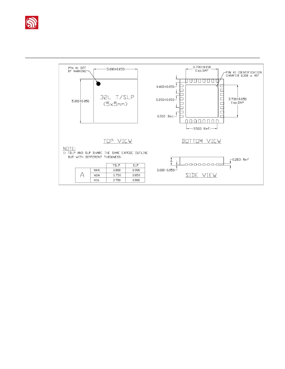
6. Package Information
6.
Package Information
!
Figure 6-1. ESP8266EX Package
Espressif
$ /$
20 24
2018.02

$
Appendix Ⅰ
I.
Appendix - Pin List
For detailed pin information, please see
.
•
Digital Die Pin List
•
Buffer Sheet
•
Register List
•
Strapping List
📖 Notes:
•
INST_NAME refers to the IO_MUX REGISTER defined in
eagle_soc.h, for example MTDI_U refers to
PERIPHS_IO_MUX_MTDI_U.
•
Net Name refers to the pin name in schematic.
•
Function refers to the multifunction of each pin pad.
•
Function number 1 ~ 5 correspond to FUNCTION 0 ~ 4 in SDK. For example, set MTDI to GPIO12 as
follows.
-
#defineFUNC_GPIO123//definedineagle_soc.h
-
PIN_FUNC_SELECT(PERIPHS_IO_MUX_MTDI_U,FUNC_GPIO12)
Espressif
$ /$
21 24
2018.02

$
Appendix Ⅱ
II.
Appendix - Learning
Resources
II.1. Must-Read Documents
•
Description: This document is a quick user guide to getting started with ESP8266. It
includes an introduction to the ESP-LAUNCHER, instructions on how to download
firmware to the board and run it, how to compile the AT application, as well as the
structure and debugging method of RTOS SDK. Basic documentation and other related
resources for the ESP8266 are also provided.
•
ESP8266 SDK Getting Started Guide
Description: This document takes ESP-LAUNCHER and ESP-WROOM-02 as examples
of how to use the ESP8266 SDK. The contents include preparations before compilation,
SDK compilation and firmware download.
•
Description: This link directs you to a list containing the type and function of every
ESP8266 pin.
•
Description: This document provides a technical description of the ESP8266 series of
products, including ESP8266EX, ESP-LAUNCHER and ESP-WROOM.
•
ESP8266 Hardware Matching Guide
Description: This document introduces the frequency offset tuning and antenna
impedance matching for ESP8266 in order to achieve optimal RF performance.
•
Description: This document provides an introduction to the interfaces integrated on
ESP8266. Functional overview, parameter configuration, function description,
application demos and other pieces of information are included.
•
Description: This zip package includes manufacturing BOMs, schematics and PCB
layouts of ESP8266 boards and modules.
•
II.2. Must-Have Resources
•
Espressif
$ /$
22 24
2018.02

$
Appendix Ⅱ
Description: This webpage provides links both to the latest version of the ESP8266 SDK
and the older ones.
•
Description: This webpage provides links to both the ESP8266 flash download tools and
the ESP8266 performance evaluation tools.
•
•
ESP8266 Certification and Test Guide
•
•
Espressif
$ /$
23 24
2018.02

Disclaimer and Copyright Notice
Information in this document, including URL references, is subject to change without
notice.
THIS DOCUMENT IS PROVIDED AS IS WITH NO WARRANTIES WHATSOEVER,
INCLUDING ANY WARRANTY OF MERCHANTABILITY, NON-INFRINGEMENT, FITNESS
FOR ANY PARTICULAR PURPOSE, OR ANY WARRANTY OTHERWISE ARISING OUT
OF ANY PROPOSAL, SPECIFICATION OR SAMPLE.
All liability, including liability for infringement of any proprietary rights, relating to use of
information in this document is disclaimed. No licenses express or implied, by estoppel or
otherwise, to any intellectual property rights are granted herein.
The Wi-Fi Alliance Member logo is a trademark of the Wi-Fi Alliance. The Bluetooth logo is
a registered trademark of Bluetooth SIG.
All trade names, trademarks and registered trademarks mentioned in this document are
property of their respective owners, and are hereby acknowledged.
Copyright © 2018 Espressif Inc. All rights reserved.
Espressif IOT Team
Document Outline
- Overview
- Wi-Fi Protocols
- Specifications
- Applications
- Pin Definitions
- Functional Description
- CPU, Memory, and Flash
- CPU
- Memory
- AHB and AHB Blocks
- Clock
- High Frequency Clock
- External Clock Requirements
- Radio
- Channel Frequencies
- 2.4 GHz Receiver
- 2.4 GHz Transmitter
- Clock Generator
- Wi-Fi
- Power Management
- Peripheral Interface
- General Purpose Input/Output Interface (GPIO)
- Secure Digital Input/Output Interface (SDIO)
- Serial Peripheral Interface (SPI/HSPI)
- General SPI (Master/Slave)
- HSPI (Slave)
- I2C Interface
- I2S Interface
- Universal Asynchronous Receiver Transmitter (UART)
- Pulse-Width Modulation (PWM)
- IR Remote Control
- ADC (Analog-to-Digital Converter)
- LED Light and Button
- Electrical Specifications
- Electrical Characteristics
- Power Consumption
- Wi-Fi Radio Characteristics
- Package Information
- Appendix - Pin List
- Appendix - Learning Resources
- Must-Read Documents
- Must-Have Resources
Wyszukiwarka
Podobne podstrony:
0A ESP8266 Datasheet EN v4 3
PENDRIVE s100 datasheet en 15
3RV20111HA10 datasheet en
6ES73211BH500AA0 datasheet en
3RA61201DP32 datasheet en
6ES73401AH020AE0 datasheet en
6AV66470AC113AX0 datasheet en
6ES73146CH040AB0 datasheet en
6ES72151AG400XB0 datasheet en (1)
6ES73146CG030AB0 datasheet en
3RK12000CQ200AA3 datasheet en
3RV20110EA10 datasheet en
TK72E08N1 datasheet en 20120529
6ES72111AE400XB0 datasheet en
en ta8029s 20020308 datasheet
EcoSolar Datasheet Phoenix Inverter 180VA 1200VA EN
Datasheet BlueSolar charge controller MPPT 75 50 & MPPT 100 50 EN
więcej podobnych podstron