
MSE Published Date: 4 March 2003
© Motorola, Inc., 2003
MSE9S12D128_1L40K
Rev 0.0, 03/2003
Mask Set Errata for
MC9S12DT128
Mask 1L40K
Mask Set Errata
This product incorporates SuperFlash® technology licensed from SST
Introduction
This errata provides information applicable to the following MCU mask sets for
the MC9S12DT128/DJ128 and DG128 devices:
•
1L40K*
*Note that the MC9S12DB128 is not available in the 1L40K mask.
MCU Device Mask Set Identification
The mask set is identified by a four-character code consisting of a letter, two
numerical digits, and a letter, for example F74B. Slight variations to the mask
set identification code may result in an optional numerical digit preceding the
standard four-character code, for example 0F74B.
MCU Device Date Codes
Device markings indicate the week of manufacture and the mask set used. The
data is coded as four numerical digits where the first two digits indicate the year
and the last two digits indicate the work week. The date code “9115” would
indicate the 15th week of the year 1991.
MCU Device Part Number Prefixes
Some MCU samples and devices are marked with an SC, PC, ZC or XC prefix.
An SC, PC or ZC prefix denotes special/custom device. An XC prefix denotes
device is tested but is not fully characterized or qualified over the full range of
normal manufacturing process variations. After full characterization and
qualification, devices will be marked with the MC prefix.
Errata System Tracking Numbers
MUCTS00xxx is the tracking number for device errata. It can be used with the
mask set and date code to identify a specific errata to a Motorola
representative.

MSE9S12D128_1L40K
2
MSE9S12D128_1L40K
Motorola
ERRATA SUMMARY
SPTEF flag set wrongly
Errata Number: MUCts00708
Description
When the SPI is enabled in master mode, with the CPHA bit set, back to back
transmissions are possible.
When a transmission completes and a further byte is available in the SPI Data
Register, the second transmission begins directly after the “minimum trailing
time”.
The problem occurs when, after the SPTEF flag has been set, a further byte is
written into the SPI Data Register during the “1st pulse” of a subsequent
transmission.
Errata
Number
Module
affected
Brief description
MUCts00708
SPI
SPTEF flag set wrongly
MUCts00735
ATD
Flags in ATDSTAT0 do not clear by writing “1”, ETORF sets wrongly
MUCts00742
SPI
SPI in mode fault state, but MISO output buffer not disabled
MUCts00755
BDM
ACK conflict exiting STOP
MUCts00756
MSCAN
Glitch filter exceeds spec limits
MUCts00757
KWU
Glitch filter exceeds upper 10
µ
s limit
MUCts00778
BYTEFLIGHT
Tx messages of same ID block subsequent lower priority IDs
MUCts00784
ATD
Write to ATDCTL5 may not clear SCF, CCF and ASCIF flags
MUCts00788
PADS
ESD fails at 2KV HBM
MUCts00793
BYTEFLIGHT
FIFO may overflow as RCVFIF is not asserted again
MUCts00799
SPI
MISO not kept after sixteenth SCK edge
MUCts00821
CRG PLL
If osc_clock is 2 to 3 times pll_clock, STOP can cause SCM or reset
MUCts00833
EEPROM
Cumulative EEPROM W/E Cycle Limit For 'V' & 'M' Rated Products
MSE9S12D128_1L40K
Motorola
MSE9S12D128_1L40K
3
Then the SPTEF flag is set at the falling SCK edge of the “1st pulse” and data
is transferred from the SPI Data Register to the transmit shift register. The
result is that the transmission is corrupted and data is lost.
Workaround
After the SPTEF flag has been set, a delay of 1/2 SCK period has to be added
before storing data into the SPI Data Register.
ATD: Flags in ATDSTAT0 do not clear by writing ‘1’, ETORF sets wrongly
Errata Number: MUCts00735
Description
For the flags SCF, ETORF and FIFOR in ATDSTAT0 it is specified that writing
a ‘1’ to the respective flag clears it. This does not work. Writing ‘1’ to the
respective flag has no effect. The ETORF flag is also set by a non-active edge,
e.g. falling edge trigger (ETRILE=0, ETRIGP=0). ETORF is set on both falling
edges and rising edges while conversion is in progress.
Workaround
SCF
1.
Use the alternative flag clearing mechanisms:
a.
Write to ATDCTL5 (a new conversion sequence is started)
b.
If AFFC=1 a result register is read
ETORF
1.
Use the alternative flag clearing mechanisms:
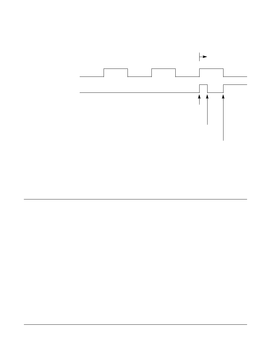
SCK
7th pulse
8th pulse
1st pulse
SPTEF
next transmission
End of transmission
SPTEF flag is being set
Write to SPIDR
during “1st pulse”
SPTEF flag set again (WRONG)

MSE9S12D128_1L40K
4
MSE9S12D128_1L40K
Motorola
a.
Write to ATDCTL2, ATDCTL3 or ATDCTL4 (a conversion sequence
is aborted)
b.
Write to ATDCTL5 (a new conversion sequence is started)
2.
Avoid external trigger edges during conversion process by using short
pulses
3.
Ignore ETROF flag
FIFOR
1.
Use the alternative flag clearing mechanism:
a.
Start a new conversion sequence (write to ATDCTL5 or external
trigger)
SPI: SPI in Mode Fault state, but MISO output buffer not disabled
Errata Number: MUCts00742
Description
When the SPI is in Mode Fault state (MODF flag set), according to the
specification, all SPI output buffers (SS, SCK, MOSI, MISO) should be
disabled. However, the MISO output buffer is not disabled.
Workaround
None
BDM: ACK conflict exiting STOP
Errata Number: MUCts00755
Description
When using the Background Debugger to debug code which contains STOP
instructions, the host debugger can lose clock sync with the target device. If the
ACK protocol is enabled, a target command which is expecting to send an ACK
pulse can conflict with a host issued SYNC command attempting to re-establish
clock sync between the host and target.
Workaround
The ACK protocol can be disabled when debugging source code which
contains STOP instructions. The host SYNC command may then be used to re-
establish clock sync between the host and target after a STOP instruction.
MSCAN: Glitch filter exceeds spec limits
Errata Number: MUCts00756
Description
The specified MSCAN wake-up glitch filter pulse limits can be exceeded. At low
temp/high VDD the module may wake up from sleep mode on glitches <2
µ
s
while for pulses >5
µ
s it may not wake up from sleep mode at high temp/low

MSE9S12D128_1L40K
Motorola
MSE9S12D128_1L40K
5
VDD. The device operates at relaxed limits: MSCAN Wake-up dominant pulse
filtered: max. 1
µ
s MSCAN Wake-up dominant pulse pass: min. 7
µ
s
Workaround
None
Key wake-up: Glitch filter exceeds upper 10
µ
s limit
Errata Number: MUCts00757
Description
The specified maximum limit of the key wake-up glitch filter pulse can be
exceeded at high temp/low VDD, i.e. the CPU may not wake up from STOP
mode on pulses
≥
10
µ
s. The device operates at a relaxed limit of 14
µ
s.
Workaround
None
BYTEFLIGHT: Tx messages of same ID block subsequent lower priority IDs
Errata Number: MUCts00778
Description
If there are two or more buffers set up with the same identifier, message
transmission takes place until the first message of the same ID messages has
been sent. All subsequent messages with lower priority are blocked from being
transmitted in the same communication cycle.
Workaround
None
ATD: Write to ATDCTL5 may not clear SCF, CCF and ASCIF flags
Errata Number: MUCts00784
Description
If a write to ATDCTL5 happens at exactly the bus cycle where an ongoing
conversion sequence ends, the SCF, CCF and (if ASCIE=1) ASCIF flags
remain set and are NOT cleared by a write to ATDCTL5.
Workaround
1.
Make sure the device is protected from interrupts (temporarily disable
interrupts with the I mask bit).
2.
Write to ATDCTL5 twice.

MSE9S12D128_1L40K
6
MSE9S12D128_1L40K
Motorola
ESD fails for 2KV HBM
Errata Number: MUCts00788
Description
ESD performance:
•
2KV HBM (Human Body Model) fails ESD tests
•
1.75KV HBM pass ESD tests
Therefore, reduced ESD spec for HBM is 1.75KV
Workaround
None
Byteflight: FIFO may overflow as RCVFIF is not asserted again
Errata Number: MUCts00793
Description
If the last message in the FIFO is read, i.e. buffer 0 is unlocked around the end
of a new incoming FIFO message, the FIFO not empty (RCVFIF) flag is not
asserted again. This will eventually result in a FIFO overflow. The time window
is about 6 osc clock cycles in which the two events must occur to cause the
problem.
Workaround
None
SPI: MISO not kept after sixteenth SCK edge
Errata Number: MUCts00799
Description
In SPI slave mode with CPHA set, MISO can change falsely after a
transmission, two to three bus clock cycles after the sixteenth SCK edge. This
can lead to a hold time violation on the SPI master side.
Workaround
There are two possible workarounds for this problem:
1.
Decrease the bus clock of the slave SPI to satisfy the “Masters MISO
Hold Time”.
Tbus(Slave)
≥
0.5 * “Masters MISO Hold Time”
2.
Software workaround:
The slave has to transmit a dummy byte after each data byte, which
must fulfill the following requirements:
•
The dummy bytes first bit to be transmitted (depending on LSBFE bit)
must be equal to the last bit of the data byte transmitted before.
The dummy byte has to be stored into SPIDR during the transmission of
the corresponding data byte.

MSE9S12D128_1L40K
Motorola
MSE9S12D128_1L40K
7
–
MISO does not change after the data byte.
•
The Master has to receive two bytes, the data byte and the dummy byte.
–
Master receives the data byte correctly and has to skip the dummy
byte.
PLL: If osc_clock is 2 to 3 times pll_clock, STOP can cause SCM or reset
Errata Number: MUCts00821
Description
This Erratum applies only to systems where PLL is used to divide down the
osc_clock by a ratio between 2 and 3. If
1.
pll_clock (PLLON=1) is running and
2.
2 < osc_clock ÷ pll_clock < 3 and
3.
Full stop mode is entered (STOP instruction with PSTP Bit =0)
there is a small possibility that when entering full stop mode the chip reacts as
follows:
1.
If self clock mode is disabled (SCME=0) a clock monitor reset will occur.
The system does NOT enter full stop mode.
2.
If self clock mode and SCM interrupt are enabled (SCME=1 and
SCMIE=1) a self clock mode interrupt is generated. The SCMIF flag is
set. The system does NOT enter full stop mode.
3.
If self clock mode is enabled and SCM interrupt is disabled (SCME=1
and SCMIE=0) the system will enter full stop mode. However, after
wakeup, self clock mode is immediately entered without performing the
specified clock quality check. The SCMIF flag will be set.
Workaround
1.
Avoid osc_clock ÷ pll_clock ratios between 2 and 3.
2.
If a osc_clock ÷ pll_clock ratio between 2 and 3 is required, perform the
following before entering full stop mode.
a.
Deselect PLL (PLLSEL=0)
b.
Turn off PLL (PLLON=0)
c.
Enter stop
d.
On exit from stop, turn on PLL again (PLLON=1)

MSE9S12D128_1L40K
8
MSE9S12D128_1L40K
Motorola
Cumulative EEPROM W/E Cycle Limit For 'V' & 'M' Rated Products
Errata Number: MUCts00833
Description
The EEPROM charge pump capabilities limit the cumulative number of sector
Program/Erase cycles at temperatures greater or equal to 105ºC ambient. ‘C’
temperature rated (85ºC) products are not affected by this errata. EEPROM
Program/Erase cycling is therefore bounded by the following 2 criteria.
1.
Any single byte or sector cannot exceed the specification of 100K
Program/Erase cycles as noted by the following:
2.
The cumulative number of sector Program/Erase cycles is bounded as
noted below:
Although the charge pump limits the cumulative number of Program/Erase
cycles, any portion of the array has high (up to 100K) Program/Erase cycle
endurance capability at elevated temperatures as demonstrated in the
following examples:
Min
Typ
Max
EEPROM number of Program/Erase cycles:
(–40ºC
≤
T
j
≤
0ºC)
n
EEPE
10,000
Cycles
EEPROM number of Program/Erase cycles:
(0ºC
≤
T
j
≤
140ºC)
n
EEPE
100,000
Cycles
Min
Typ
Max
EEPROM number of sector
125ºC (M)
cumulative Program/Erase
105ºC (V)
cycles
85ºC (C)
n
MAX
20.0M
30.0M
51.2M
(1)
Cycles
1. Note that 51.2M sector cycles is equivalent to 100,000 full array (2048 bytes = 512 sectors) cycles as commonly specified.

MSE9S12D128_1L40K
Motorola
MSE9S12D128_1L40K
9
Examples
•
MC9S12Dx128 EEPROM has 512 EEPROM sectors (1 sector = 4
Bytes)
•
Definitions:
X = Number of sectors
⇔
X
≤
512 sectors
Y = Number of Prog/Erase cycles for all X sectors
⇔
Y
≤
100K cycs (spec)
X*Y = Cumulative Number of Program/Erase cycles for the X sectors
85ºC Temperature, 'C' rated product:
•
Capability: Full specification
=> 512 sectors (full array) x 100,000 Cycles
≤
51.2 M cycles
105ºC & 125ºC Temperature, 'V' and 'M' rated product:
•
Capability: Reduced cumulative number of Program/Erase cycles:
125ºC:
≤
20M Cycles
105ºC:
≤
30M Cycles
=> Using the above formula for an application that requires a portion of the
EEPROM array at high endurance (up to 100K) and other portions for lesser
endurance needs, the following is an example calculation for total cumulative
cycles at 125ºC:
128 sectors (
¼
array) x 100K cycs + 256 sectors (
½
array) x 25K cycs + 128
sectors (
¼
array) x 1000 cycs < 20M cycles
Workaround
None
Xi
Yi
×
i
1
=
n
å
Xi
Yi
×
i
1
=
n
å

MSE9S12D128_1L40K
HOW TO REACH US:
USA/EUROPE/LOCATIONS NOT LISTED:
Motorola Literature Distribution;
P.O. Box 5405, Denver, Colorado 80217
1-303-675-2140 or 1-800-441-2447
JAPAN:
Motorola Japan Ltd.; SPS, Technical Information Center,
3-20-1, Minami-Azabu Minato-ku, Tokyo 106-8573 Japan
81-3-3440-3569
ASIA/PACIFIC:
Motorola Semiconductors H.K. Ltd.;
Silicon Harbour Centre, 2 Dai King Street,
Tai Po Industrial Estate, Tai Po, N.T., Hong Kong
852-26668334
TECHNICAL INFORMATION CENTER:
1-800-521-6274
HOME PAGE:
http://motorola.com/semiconductors
Information in this document is provided solely to enable system and software
implementers to use Motorola products. There are no express or implied copyright
licenses granted hereunder to design or fabricate any integrated circuits or
integrated circuits based on the information in this document.
Motorola reserves the right to make changes without further notice to any products
herein. Motorola makes no warranty, representation or guarantee regarding the
suitability of its products for any particular purpose, nor does Motorola assume any
liability arising out of the application or use of any product or circuit, and specifically
disclaims any and all liability, including without limitation consequential or incidental
damages. “Typical” parameters which may be provided in Motorola data sheets
and/or specifications can and do vary in different applications and actual
performance may vary over time. All operating parameters, including “Typicals”
must be validated for each customer application by customer’s technical experts.
Motorola does not convey any license under its patent rights nor the rights of
others. Motorola products are not designed, intended, or authorized for use as
components in systems intended for surgical implant into the body, or other
applications intended to support or sustain life, or for any other application in which
the failure of the Motorola product could create a situation where personal injury or
death may occur. Should Buyer purchase or use Motorola products for any such
unintended or unauthorized application, Buyer shall indemnify and hold Motorola
and its officers, employees, subsidiaries, affiliates, and distributors harmless
against all claims, costs, damages, and expenses, and reasonable attorney fees
arising out of, directly or indirectly, any claim of personal injury or death associated
with such unintended or unauthorized use, even if such claim alleges that Motorola
was negligent regarding the design or manufacture of the part.
Motorola and the Stylized M Logo are registered in the U.S. Patent and Trademark
Office. digital dna is a trademark of Motorola, Inc. All other product or service
names are the property of their respective owners. Motorola, Inc. is an Equal
Opportunity/Affirmative Action Employer.
© Motorola, Inc. 2003
MSE9S12D128_1L40K
Rev 0.0
Additional mask set erratas can be found on the World Wide Web at
http://motorola.com/semiconductors
.
Document Outline
- Introduction
- MCU Device Mask Set Identification
- MCU Device Date Codes
- MCU Device Part Number Prefixes
- Errata System Tracking Numbers
- ERRATA SUMMARY
- SPTEF flag set wrongly Errata Number: MUCts00708
- ATD: Flags in ATDSTAT0 do not clear by writing ‘1’, ETORF sets wrongly Errata Number: MUCts00735
- SPI: SPI in Mode Fault state, but MISO output buffer not disabled Errata Number: MUCts00742
- BDM: ACK conflict exiting STOP Errata Number: MUCts00755
- MSCAN: Glitch filter exceeds spec limits Errata Number: MUCts00756
- Key wake-up: Glitch filter exceeds upper 10ms limit Errata Number: MUCts00757
- BYTEFLIGHT: Tx messages of same ID block subsequent lower priority IDs Errata Number: MUCts00778
- ATD: Write to ATDCTL5 may not clear SCF, CCF and ASCIF flags Errata Number: MUCts00784
- ESD fails for 2KV HBM Errata Number: MUCts00788
- Byteflight: FIFO may overflow as RCVFIF is not asserted again Errata Number: MUCts00793
- SPI: MISO not kept after sixteenth SCK edge Errata Number: MUCts00799
- PLL: If osc_clock is 2 to 3 times pll_clock, STOP can cause SCM or reset Errata Number: MUCts00821
- Cumulative EEPROM W/E Cycle Limit For 'V' & 'M' Rated Products Errata Number: MUCts00833
Wyszukiwarka
Podobne podstrony:
MC9S12H256 Mask Set Errata 2
MC9S12A128 Mask Set Errata
MC9S12D64 Mask Set Errata 2
MC9S12D64 Mask Set Errata 3
MC9S12DT128 Mask Set Errata 2
MC68HC912B32 Mask Set Errata 1
MC68HC912B32 Mask Set Errata 1
MC68HC912BC32 Mask Set Errata 2
MC68HC12BE32 Mask Set Errata 4
MC68HC12D60 Mask Set Errata 1
MC68HC812A4 Mask Set Errata 1
PC9S12D64 PC9S12DJ64 Mask Set Errata 1
MC68HC912DG128A Mask Set Errata 1
MC68HC912D60C Mask Set Errata 1
MC68HC912BC32 Mask Set Errata 1
MC68HC12BE32 Mask Set Errata 3
PC9S12H256 Mask Set Errata 1
MC68HC912D60A Mask Set Errata 1
więcej podobnych podstron