
MOTOROLA
SEMICONDUCTOR TECHNICAL INFORMATION
PC9S12D64MSE1 Rev 2
September 25, 2002
When contacting a Motorola representative for assistance, please have the MCU
device mask set and date code information available.
Specifications and information herein are subject to change without notice.
© Motorola, Inc., 2002
MSE Published Date: September 25, 2002
Mask Set Errata 1
PC9S12D64* Microcontroller Unit
(*Devices covered: PC9S12D64 and PC9S12DJ64)
INTRODUCTION
This errata provides information applicable to the following MCU mask set devices:
•
0L86D mask
MCU DEVICE MASK SET IDENTIFICATION
The mask set is identified by a four-character code consisting of a letter, two
numerical digits, and a letter, for example F74B. Slight variations to the mask set
identification code may result in an optional numerical digit preceding the standard
four-character code, for example 0F74B.
MCU DEVICE DATE CODES
Device markings indicate the week of manufacture and the mask set used. The
data is coded as four numerical digits where the first two digits indicate the year
and the last two digits indicate the work week. The date code “9115” would indicate
the 15th week of the year 1991.
MCU DEVICE PART NUMBER PREFIXES
Some MCU samples and devices are marked with an SC, PC, ZC or XC prefix. An
SC, PC or ZC prefix denotes special/custom device. An XC prefix denotes device
is tested but is not fully characterized or qualified over the full range of normal
manufacturing process variations. After full characterization and qualification,
devices will be marked with the MC prefix (or SC for some custom parts).

2
PC9S12D64MSE1 Rev 2
September 25, 2002
ERRATA SYSTEM TRACKING NUMBERS
MUCTS00xxx is the tracking number for device errata. It can be used with the
mask set and date code to identify a specific errata to a Motorola representative.
ERRATA SUMMARY
KEY WAKE-UP: GLITCH FILTER EXCEEDS UPPER 10
µ
S LIMIT MUCTS00628
The specified maximum limit of the key wake-up glitch filter pulse can be exceeded
at high temp/low VDD, i.e. the CPU may not wake up from STOP mode on pulses
>=10
µ
s. The device operates at a relaxed limit of 14
µ
s.
Work-
around
None
Errata
Number
Module
affected
Brief description
Workaround
available?
First
Issued
MUCts00628
KWU
Key wake-up: Glitch filter exceeds upper 10
µ
s limit
No
Rev 0
MUCts00636
MSCAN
Glitch filter exceeds spec limits
No
Rev 0
MUCts00640
EEPROM
Program & Erase of EEPROM blocked in Normal Single Chip
Mode when secure
Yes
Rev 0
MUCts00645
FLASH
Program & Erase of Flash blocked in Normal Single Chip Mode
when secure
Yes
Rev 0
MUCts00681
BDM
Spurious SYNC pulse
Yes
Rev 0
MUCts00692
ESD
ESD fails for 2KV HBM
No
Rev 0
MUCts00708
SPI
SPTEF flag set wrongly
Yes
Rev 1
MUCts00738
ATD
Flags in ATDSTAT0 do not clear by writing "1", ETORF sets
wrongly
Yes
Rev 1
MUCts00742
SPI
SPI in mode fault state, but MISO output buffer not disabled
No
Rev 1

PC9S12D64MSE1 Rev 2
3
September 25, 2002
MSCAN: GLITCH FILTER EXCEEDS SPEC LIMITS
MUCTS00636
The specified MSCAN wake-up glitch filter pulse limits can be exceeded. At low
temp/high VDD the module may wake up from sleep mode on glitches <2
µ
s while
for pulses >5
µ
s it may not wake up from sleep mode at high temp/low VDD. The
device operates at relaxed limits:
MSCAN Wake-up dominant pulse filtered: max. 1
µ
s
MSCAN Wake-up dominant pulse pass: min. 7
µ
s
Work-
around
None
PROGRAM & ERASE OF EEPROM BLOCKED IN NORMAL SINGLE CHIP
MODE WHEN SECURE
MUCTS00640
In normal single chip mode, when security is enabled, it is not possible to launch
the Program ($20), Sector-Erase ($40), Sector-Modify ($60) and Erase-Verify
($05) commands in the EEPROM. The Mass-Erase ($41) command can be
launched.
Work-
around
To enable the Program ($20), Sector-Erase ($40) and Erase-Verify ($05)
commands in the flash, security must be disabled via the backdoor key sequence.
See Flash User Guide for details of the backdoor key operation.
PROGRAM & ERASE OF FLASH BLOCKED IN NORMAL SINGLE CHIP MODE
WHEN SECURE
MUCTS00645
In normal single chip mode, when security is enabled, it is not possible to launch
the Program ($20), Sector-Erase ($40) and Erase- Verify ($05) commands in the
Flash. The Mass-Erase ($41) command can be launched.
Work-
around
To enable the Program ($20), Sector-Erase ($40) and Erase-Verify ($05)
commands in the flash, security must be disabled via the backdoor key sequence.
See Flash User Guide for details of the backdoor key operation.

4
PC9S12D64MSE1 Rev 2
September 25, 2002
SPURIOUS SYNC PULSE
MUCTS00681
A spurious BDM SYNC pulse could be transmitted if the delay between commands
is such that the first negative edge of a new command occurs exactly 128 cycles
after the last negative edge of the previous command.
Work-
around
Keep the delay between commands greater than 128 cycles.
ESD FAILS FOR 2KV HBM
MUCTS00692
ESD performance:
•
2KV HBM (Human Body Model) fails ESD tests
•
1.75KV HBM pass ESD tests
Therefore, reduced ESD spec for HBM is 1.75KV
Work-
around
None
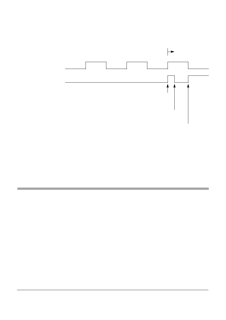
SPTEF FLAG SET WRONGLY
MUCTS00708
When the SPI is enabled in master mode, with the CPHA bit set, back to back
transmissions are possible.
When a transmission completes and a further byte is available in the SPI Data
Register, the second transmission begins directly after the “minimum trailing time”.
The problem occurs when, after the SPTEF flag has been set, a further byte is
written into the SPI Data Register during the “1st pulse” of a subsequent
transmission.
PC9S12D64MSE1 Rev 2
5
September 25, 2002
Then the SPTEF flag is set at the falling SCK edge of the “1st pulse” and data is
transferred from the SPI Data Register to the transmit shift register. The result is
that the transmission is corrupted and data is lost.
Work-
around
After the SPTEF flag has been set, a delay of 1/2 SCK period has to be added
before storing data into the SPI Data Register.
ATD: FLAGS IN ATDSTAT0 DO NOT CLEAR BY WRITING ‘1’, ETORF SETS
WRONGLY
MUCTS00738
For the flags SCF, ETORF and FIFOR in ATDSTAT0 it is specified that: Write ‘1’
to the respective flag clears it. This does not work. Writing ‘1’ to the respective flag
has no effect. The ETORF flag is also set by a non active edge, e.g. falling edge
trigger (ETRILE=0, ETRIGP=0). ETORF is set on both falling edges and rising
edges while conversion is in progress.
Work-
around
SCF
1. Use the alternative flag clearing mechanisms:
a. Write to ATDCTL5 (a new conversion sequence is started)
b. If AFFC=1 and read of a result register
SCK
7th pulse
8th pulse
1st pulse
SPTEF
next transmission
End of transmission
SPTEF flag is being set
Write to SPIDR
during “1st pulse”
SPTEF flag set again (WRONG)

PC9S12D64MSE1
Motorola reserves the right to make changes without further notice to any products herein. Motorola makes no warranty, representation or guarantee regarding the suitability of its
products for any particular purpose, nor does Motorola assume any liability arising out of the application or use of any product or circuit, and specifically disclaims any and all liability,
including without limitation consequential or incidental damages. "Typical" parameters which may be provided in Motorola data sheets and/or specifications can and do vary in different
applications and actual performance may vary over time. All operating parameters, including "Typicals" must be validated for each customer application by customer’s technical experts.
Motorola does not convey any license under its patent rights nor the rights of others. Motorola products are not designed, intended, or authorized for use as components in systems
intended for surgical implant into the body, or other applications intended to support or sustain life, or for any other application in which the failure of the Motorola product could create a
situation where personal injury or death may occur. Should Buyer purchase or use Motorola products for any such unintended or unauthorized application, Buyer shall indemnify and hold
Motorola and its officers, employees, subsidiaries, affiliates, and distributors harmless against all claims, costs, damages, and expenses, and reasonable attorney fees arising out of,
directly or indirectly, any claim of personal injury or death associated with such unintended or unauthorized use, even if such claim alleges that Motorola was negligent regarding the
design or manufacture of the part. Motorola and
are registered trademarks of Motorola, Inc. Motorola, Inc. is an Equal Opportunity/Affirmative Action Employer.
Additional mask set errata can be found on the World Wide Web at http://www.mcu.motsps.com/documentation/index.html
September 25, 2002
ETORF
1. Use the alternative flag clearing mechanisms:
a. Write to ATDCTL2, ATDCTL3 or ATDCTL4 (a conversion sequence is
aborted)
b. Write to ATDCTL5 (a new conversion sequence is started)
2. Avoid external trigger edges during conversion process by using short
pulses
3. Ignore ETROF flag
FIFOR
1. Use the alternative flag clearing mechanism:
a. Start a new conversion sequence (write to ATDCTL5 or external trigger)
SPI: SPI IN MODE FAULT STATE, BUT MISO OUTPUT BUFFER NOT
DISABLED
MUCTS00742
When the SPI is in Mode Fault state (MODF flag set), according to the
specification, all SPI output buffers (SS, SCK, MOSI, MISO) should be disabled.
However, the MISO output buffer is not disabled.
Work-
around
None
Document Outline
- introduction
- MCU Device Mask Set Identification
- MCU Device Date Codes
- MCU Device Part Number Prefixes
- Errata System Tracking Numbers
- ERRATA SUMMARY
- Key wake-up: Glitch filter exceeds upper 10ms limit MUCts00628
- MSCAN: Glitch filter exceeds spec limits MUCts00636
- Program & Erase of EEPROM blocked in Normal Single Chip Mode when secure MUCts00640
- Program & Erase of Flash blocked in Normal Single Chip Mode when secure MUCts00645
- Spurious SYNC pulse MUCts00681
- ESD fails for 2KV HBM MUCts00692
- SPTEF flag set wrongly MUCts00708
- ATD: Flags in ATDSTAT0 do not clear by writing ‘1’, ETORF sets wrongly MUCts00738
- SPI: SPI in Mode Fault state, but MISO output buffer not disabled MUCts00742
Wyszukiwarka
Podobne podstrony:
PC9S12H256 Mask Set Errata 1
MC68HC912B32 Mask Set Errata 1
MC68HC912B32 Mask Set Errata 1
MC68HC912BC32 Mask Set Errata 2
MC68HC12BE32 Mask Set Errata 4
MC68HC12D60 Mask Set Errata 1
MC68HC812A4 Mask Set Errata 1
MC9S12H256 Mask Set Errata 2
MC68HC912DG128A Mask Set Errata 1
MC9S12A128 Mask Set Errata
MC68HC912D60C Mask Set Errata 1
MC68HC912BC32 Mask Set Errata 1
MC9S12DT128 Mask Set Errata 1
MC68HC12BE32 Mask Set Errata 3
MC68HC912D60A Mask Set Errata 1
MC68HC812A4 Mask Set Errata 2
MC68HC912DT128A Mask Set Errata 1
MC9S12D64 Mask Set Errata 2
więcej podobnych podstron