
MSE Published Date: 26 March 2003
© Motorola, Inc., 2003
MSE912DG128C_1L05H
Rev 0.0, 01/2003
Mask Set Errata for
68HC912DG128C
Mask 1L05H
Mask Set Errata
This product incorporates SuperFlash® technology licensed from SST
Introduction
This mask set errata applies to the following MCU mask set:
•
1L05H
MCU Device Mask Set Identification
The mask set is identified by a 5-character code consisting of a version
number, a letter, two numerical digits, and a letter, for example 0K51E. All
standard devices are marked with a mask set number and a date code.
MCU Device Date Codes
Device markings indicate the week of manufacture and the mask set used. The
date is coded as four numerical digits where the first two digits indicate the year
and the last two digits indicate the work week. For instance, the date code
“0201” indicates the first week of the year 2002.
MCU Device Part Number Prefixes
Some MCU samples and devices are marked with an SC, PC, or XC prefix. An
SC prefix denotes special/custom device. A PC prefix indicates a prototype
device which has undergone basic testing only. An XC prefix denotes that the
device is tested but is not fully characterized or qualified over the full range of
normal manufacturing process variations. After full characterization and
qualification, devices will be marked with the MC or SC prefix.

MSE912DG128C_1L05H
2
MSE912DG128C_1L05H
MOTOROLA
Errata Summary
Abort in last ATDCLK of sequence does not restart
Errata Number: HC12_AR_659
Description
When writing ATDCTL4 and/or ATDCTL5 during an active conversion the write
is considered an abort and restart. However, when writing during the last
ATDCLK of a sequence, the current conversion is aborted, but a new
conversion is not started. This occurs whether the sequence is 1 or 4 or 8
conversions. Since writes to ATDCTL4 start a conversion then it is possible for
successive byte writes to ATDCTL4/5 to result in this problem. This would
occur if an IRQ service related to another interrupt source occurs, separating
the two byte writes, and the RTI of this returns delaying the second write to
occur in the last ATDCLK.
Workaround
The first aspect of the solution is to use word writes to ATDCTL4/5. This
eliminates the possibility of other IRQ sources causing delay between writes to
ATDCTL4/5. This would be the only solution required when starting the first
conversion. It would also be the only solution needed when SCAN=0 if all
further conversion sequences are initiated from an ATD interrupt routine. In
addition, this is the only solution needed if code, in general, does not abort
ongoing conversions.
The second aspect to the solution regards cases that abort conversions. The
easiest solution is to toggle the S8C bit. This effectively cleans up the abort and
the second write to the ATDCTL5 will perform a successful restart. Bracket this
toggle sequence with SEI and CLI to prevent the second write from occurring
during a last ATDCLK of a sequence.
Errata
number
Module
affected
Description
AR_659
ATD
Abort in last ATDCLK of sequence does not restart
AR_593
CGM
Operation with 16MHz quartz crystals is not recommended
AR_650
CGM
XIRQ during last cycle of STOP instruction causes run away
AR_644
ECT
PA Overflow flag not set when event is concurrent with write of $FFFF
AR_526
IIC
SCL divider has an extra clock at 8Mhz bus frequency
AR_573
IIC
IIC hold both SCL and SDA lines low when IBB bit is not busy
AR_548
IIC
Disabling IIC can glitch and corrupt IIC bus
AR_646
MSCAN
MSCAN extended ID rejected if stuff bit between ID16 and ID15

MSE912DG128C_1L05H
Operation with 16MHz quartz crystals is not recommended Errata Number: HC12_AR_593
MOTOROLA
MSE912DG128C_1L05H
3
Another method is possible using dual writes to start a conversion with a
minimum of one ATDCLK period between the writes. This effectively allows the
first write to abort and flush by the next write which would start (or restart) the
conversion. The second write also needs to occur before another sequence
complete time elapses. This method should also be prefixed by a SEI and
followed by a CLI. This would prevent the case of other IRQ sources causing
the same problem as well.
Operation with 16MHz quartz crystals is not recommended
Errata Number: HC12_AR_593
Description
Interaction of the resonator and microcontroller characteristics can result in a
small proportion of applications failing to start up and stabilize correctly even
though typical product combinations work well under test conditions. Resonator
operation should be restricted to maximum 10 MHz
Workaround
1.
Use 10 MHz (or slower) resonators and generate higher bus frequencies
using the PLL module. Note: When using 10 MHz or slower resonators
proper and robust operation of the oscillator circuit requires close
attention to board layout to ensure correct gain margin and negative
resistance margin. There is a well documented analysis technique
performed to measure Negative Resistance Margin which indicates the
margin for stable oscillation of the combined microcontroller and
resonator. However, an alternative approach is to include gain margin
analysis. Since a negative resistance margin optimization cannot
include all process, temperature, and voltage variance of the
microcontroller, it is possible that the components chosen for the
optimum negative resistance point may not yield acceptable component
values for gain margin. In this case a compromise between the negative
resistance margin and gain margin is desired. However option 2 (below)
may be necessary should this remain unachievable.
2.
The EXTAL pin input accepts frequencies greater than 10 MHz. In this
case, use of an external quartz oscillator module or other source of
externally generated clocks at the desired frequency, up to the 16 MHz
specification, will allow the MCU to function correctly.
XIRQ during last cycle of STOP instruction causes run away
Errata Number: HC12_AR_650
Description
If an XIRQ interrupt occurs during the execution of the STOP instruction with
the control bit DLY=0 (located in the INTCR register), the CPU may not run the
software code as designed.

MSE912DG128C_1L05H
4
MSE912DG128C_1L05H
MOTOROLA
Workaround
1.
Set the delay control bit DLY=1 so that a delay will be imposed prior to
coming out of STOP.
2.
If using XIRQ with a stable external clock and DLY=0, contact Motorola
Applications Department for a detailed workaround.
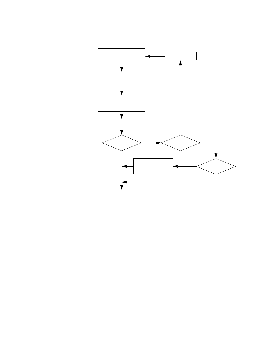
PA Overflow flag not set when event is concurrent with write of $FFFF
Errata Number: HC12_AR_644
Description
When the value $FFFF is written to PACA or PACB and, at the same time, an
external clocking pulse is applied to the PAC, the pulse accumulator may
overflow from $FFFF to $0000, but the pulse accumulator overflow flag
[PAFLG,PBFLG] is not set. Same situation may happen with 8-bit pulse
accumulators PAC1 and PAC3.
Workaround
The input capture function for the subject channel be enabled prior to writing a
value to the PACA or PACB. Write to the pulse accumulator register. Then do
one NOP (to allow the input capture to update the interrupt flag) followed by a
read of the input capture interrupt flag to see if it set. If yes, a check must be
made for a missing pulse accumulator event. Steps for software workaround to
see if event happens while writing to PAC:
1.
Enable Input Capture on same pin as the pulse accumulator (and same
type of event).
2.
Clear the appropriate CxF in the timer interrupt flag register.
3.
Read PAC and store as “Old PAC”.
4.
Calculate desired PAC value and write it to the PAC.
5.
Execute 1 NOP.
6.
Read CxF in the timer interrupt flag register.
If flag is not set, done (no events happened while writing to the PAC).
If flag is set read PAC
If “Old PAC” = PAC, then update PAC (event happened while writing
to PAC and the PAC did not capture it). Note, if the updated PAC value
is $00 jump to PACOV ISR.
If “Old PAC” does not equal PAC, does PAC = $00 ?
If yes, jump to PACOV ISR.
If no, done (event happened while writing to the PAC and PAC
captured it). Read CxF in the timer interrupt.
MSE912DG128C_1L05H
SCL divider has an extra clock at 8Mhz bus frequency Errata Number: HC12_AR_526
MOTOROLA
MSE912DG128C_1L05H
5
SCL divider has an extra clock at 8Mhz bus frequency
Errata Number: HC12_AR_526
Description
At maximum system frequency, the IIC bus rate slows down as much as 5%.
Workaround
Communication rate will be adjusted automatically to slower rate.
& clear CxF
Enable Input capture
Read PAC & store as
Calc next PAC value &
Execute NOP
Is TICx flag
set?
Is "Old PAC"
= PAC?
Y
N
Y
N
Is PAC
= $00?
Y
N
Update PAC
Jmp to PACOV
ISR
"Old PAC"
write it to PAC

MSE912DG128C_1L05H
6
MSE912DG128C_1L05H
MOTOROLA
IIC hold both SCL and SDA lines low when IBB bit is not busy
Errata Number: HC12_AR_573
Description
If SCL line is pulled low when generating a start signal the device will lock up.
Workaround
After trying to generate a START signal and neither the IBB nor IBAL bits are
set after several cycles, the IIC should be disabled and reenabled with the IBEN
bit.
Disabling IIC can glitch and corrupt IIC bus
Errata Number: HC12_AR_548
Description
If the IIC module is disabled by clearing the IBEN bit in IBCR register, the SDA
and SCL lines in the IIC bus will glitch to zero if PORTIB bits 6 and 7 are zero.
Workaround
Set PORTIB bits 6 and 7 to one prior to clearing IBEN bit in IBCR register.
MSCAN extended ID rejected if stuff bit between ID16 and ID15
Errata Number: HC12_AR_646
Description
For 32-bit and 16-bit identifier acceptance modes, an extended ID CAN frame
with a stuff bit between ID16 and ID15 can be erroneously rejected, depending
on IDAR0, IDAR1, and IDMR1.
Extended IDs (ID28-ID0) which generate a stuff bit between ID16 and ID15:
where
x = 0 or 1 (don't care)
*
= pattern for ID28 to ID18 (see following).
Affected extended IDs (ID28 - ID18) patterns:
a. xxxxxxxxx01
exceptions:00000000001
01111100001
xxxx1000001 except 11111000001
b. xxxxx100000
exception: 01111100000
c. xxxx0111111
exception: 00000111111
d. x0111110000
e. 10000000000
f. 11111111111
IDAR0
IDAR1
IDAR2
IDAR3
********
***1111x
xxxxxxxx
xxxxxxxx

MSE912DG128C_1L05H
MSCAN extended ID rejected if stuff bit between ID16 and ID15 Errata Number: HC12_AR_646
MOTOROLA
MSE912DG128C_1L05H
7
g. 10000011111
When an affected ID is received, an incorrect value is compared to the 2nd byte
of the filter (IDAR1 and IDAR5, plus IDAR3 and IDAR7 in 16-bit mode). This
incorrect value is the shift register contents before ID15 is shifted in (i.e. right
shifted by 1).
Workaround
If the problematic IDs cannot be avoided, the workaround is to mask certain bits
with IDMR1 (and IDMR5, plus IDMR3 and IDMR7 in 16-bit mode).
Example 1: to receive the message IDs
xxxx xxxx x011 111x xxxx xxxx xxxx xxxx
IDMR1 etc. must be 111x xxx1, i.e. ID20,19,18,15 must be masked.
Example 2: to receive the message IDs
xxxx 0111 1111 111x xxxx xxxx xxxx xxxx
IDMR1 etc. must be 1xxx xxx1, i.e. ID20 and ID15 must be masked.
In general, using IDMR1 etc. 1111 xxx1, i.e. masking ID20,19,18,SRR,15,
hides the problem

MSE912DG128C_1L05H
HOW TO REACH US:
USA/EUROPE/LOCATIONS NOT LISTED:
Motorola Literature Distribution;
P.O. Box 5405, Denver, Colorado 80217
1-303-675-2140 or 1-800-441-2447
JAPAN:
Motorola Japan Ltd.; SPS, Technical Information Center,
3-20-1, Minami-Azabu Minato-ku, Tokyo 106-8573 Japan
81-3-3440-3569
ASIA/PACIFIC:
Motorola Semiconductors H.K. Ltd.;
Silicon Harbour Centre, 2 Dai King Street,
Tai Po Industrial Estate, Tai Po, N.T., Hong Kong
852-26668334
TECHNICAL INFORMATION CENTER:
1-800-521-6274
HOME PAGE:
http://motorola.com/semiconductors
Information in this document is provided solely to enable system and software
implementers to use Motorola products. There are no express or implied copyright
licenses granted hereunder to design or fabricate any integrated circuits or
integrated circuits based on the information in this document.
Motorola reserves the right to make changes without further notice to any products
herein. Motorola makes no warranty, representation or guarantee regarding the
suitability of its products for any particular purpose, nor does Motorola assume any
liability arising out of the application or use of any product or circuit, and specifically
disclaims any and all liability, including without limitation consequential or incidental
damages. “Typical” parameters which may be provided in Motorola data sheets
and/or specifications can and do vary in different applications and actual
performance may vary over time. All operating parameters, including “Typicals”
must be validated for each customer application by customer’s technical experts.
Motorola does not convey any license under its patent rights nor the rights of
others. Motorola products are not designed, intended, or authorized for use as
components in systems intended for surgical implant into the body, or other
applications intended to support or sustain life, or for any other application in which
the failure of the Motorola product could create a situation where personal injury or
death may occur. Should Buyer purchase or use Motorola products for any such
unintended or unauthorized application, Buyer shall indemnify and hold Motorola
and its officers, employees, subsidiaries, affiliates, and distributors harmless
against all claims, costs, damages, and expenses, and reasonable attorney fees
arising out of, directly or indirectly, any claim of personal injury or death associated
with such unintended or unauthorized use, even if such claim alleges that Motorola
was negligent regarding the design or manufacture of the part.
Motorola and the Stylized M Logo are registered in the U.S. Patent and Trademark
Office. digital dna is a trademark of Motorola, Inc. All other product or service
names are the property of their respective owners. Motorola, Inc. is an Equal
Opportunity/Affirmative Action Employer.
© Motorola, Inc. 2003
MSE912DG128C_1L05H
Rev 0.0
Additional mask set erratas can be found on the World Wide Web at
http://motorola.com/semiconductors
.
Document Outline
- Introduction
- MCU Device Mask Set Identification
- MCU Device Date Codes
- MCU Device Part Number Prefixes
- Errata Summary
- Abort in last ATDCLK of sequence does not restart Errata Number: HC12_AR_659
- Operation with 16MHz quartz crystals is not recommended Errata Number: HC12_AR_593
- XIRQ during last cycle of STOP instruction causes run away Errata Number: HC12_AR_650
- PA Overflow flag not set when event is concurrent with write of $FFFF Errata Number: HC12_AR_644
- SCL divider has an extra clock at 8Mhz bus frequency Errata Number: HC12_AR_526
- IIC hold both SCL and SDA lines low when IBB bit is not busy Errata Number: HC12_AR_573
- Disabling IIC can glitch and corrupt IIC bus Errata Number: HC12_AR_548
- MSCAN extended ID rejected if stuff bit between ID16 and ID15 Errata Number: HC12_AR_646
Wyszukiwarka
Podobne podstrony:
MC68HC912B32 Mask Set Errata 1
MC68HC912B32 Mask Set Errata 1
MC68HC912BC32 Mask Set Errata 2
MC68HC12BE32 Mask Set Errata 4
MC68HC12D60 Mask Set Errata 1
MC68HC812A4 Mask Set Errata 1
MC68HC912DG128A Mask Set Errata 1
MC68HC912D60C Mask Set Errata 1
MC68HC912BC32 Mask Set Errata 1
MC68HC12BE32 Mask Set Errata 3
MC68HC912D60A Mask Set Errata 1
MC68HC812A4 Mask Set Errata 2
MC68HC912DT128A Mask Set Errata 1
MC68HC08AZ32 Mask Set Errata
MC68HC12BE32 Mask Set Errata 1
PC9S12D64 PC9S12DJ64 Mask Set Errata 1
MC9S12H256 Mask Set Errata 2
MC9S12A128 Mask Set Errata
więcej podobnych podstron