5-81
FAST AND LS TTL DATA
4-BIT BINARY FULL ADDER
WITH FAST CARRY
The SN54 / 74LS83A is a high-speed 4-Bit binary Full Adder with internal
carry lookahead. It accepts two 4-bit binary words (A1–A4, B1–B4) and a
Carry Input (C0). It generates the binary Sum outputs
∑
1 –
∑
4) and the Carry
Output (C4) from the most significant bit. The LS83A operates with either
active HIGH or active LOW operands (positive or negative logic). The
SN54 / 74LS283 is recommended for new designs since it is identical in
function with this device and features standard corner power pins.
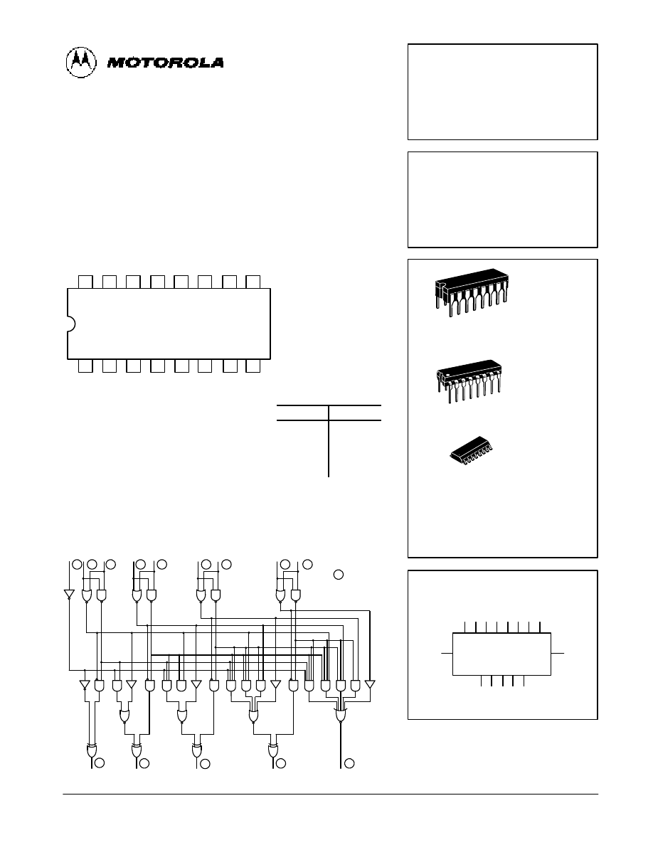
14
13
12
11
10
9
1
2
3
4
5
6
B4
7
16
15
8
Σ
4
C4
C0
GND
B1
A1
Σ
1
A4
Σ
3
A3
Σ
2
B2
A2
CONNECTION DIAGRAM DIP (TOP VIEW)
B3
VCC
NOTE:
The Flatpak version has the
same pinouts (Connection
Diagram) as the Dual In-Line
Package.
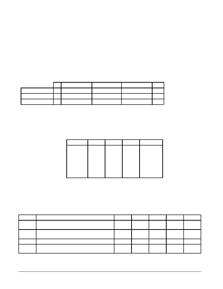
PIN NAMES
LOADING (Note a)
HIGH
LOW
A1 – A4
B1 – B4
C0
Σ
1 –
Σ
4
C4
Operand A Inputs
Operand B Inputs
Carry Input
Sum Outputs (Note b)
Carry Output (Note b)
1.0 U.L.
1.0 U.L.
0.5 U.L.
10 U.L.
10 U.L.
0.5 U.L.
0.5 U.L.
0.25 U.L.
5 (2.5) U.L.
5 (2.5) U.L.
NOTES:
a) 1 TTL Unit Load (U.L.) = 40
µ
A HIGH/1.6 mA LOW.
b) The Output LOW drive factor is 2.5 U.L. for Military (54) and 5 U.L. for Commercial (74)
Temperature Ranges.
SN54/74LS83A
4-BIT BINARY FULL ADDER
WITH FAST CARRY
LOW POWER SCHOTTKY
J SUFFIX
CERAMIC
CASE 620-09
N SUFFIX
PLASTIC
CASE 648-08
16
1
16
1
ORDERING INFORMATION
SN54LSXXJ
Ceramic
SN74LSXXN
Plastic
SN74LSXXD
SOIC
16
1
D SUFFIX
SOIC
CASE 751B-03
LOGIC SYMBOL
10 11 8 7 3 4 1 16
9 6 2 15 14
13
14
C0
B1 A2 B2 A3 B3 A4 B4
C4
∑
1
∑
2
∑
3
∑
4 C4
LOGIC DIAGRAM
VCC = PIN 5
GND = PIN 12
= PIN NUMBERS
C1
C2
C3
C0 A1
B1
A2
B2
A3 B3
A4
B4
C4
∑
1
∑
2
∑
3
∑
4
15
3
4
10
11
16
1
2
6
7
9
13
8
14
5-82
FAST AND LS TTL DATA
SN54/74LS83A
FUNCTIONAL DESCRIPTION
The LS83A adds two 4-bit binary words (A plus B) plus the incoming carry. The binary sum appears on the sum outputs (
∑
1 –
∑
4)
and outgoing carry (C4) outputs.
C0 + (A1+B1)+2(A2+B2)+4(A3+B3)+8(A4+B4) =
∑
1+2
∑
2+4
∑
3+8
∑
4+16C4
Where: (+) = plus
Due to the symmetry of the binary add function the LS83A can be used with either all inputs and outputs active HIGH (positive
logic) or with all inputs and outputs active LOW (negative logic). Note that with active HIGH Inputs, Carry Input can not be left open,
but must be held LOW when no carry in is intended.
Example:
C0
A1
A2
A3
A4
B1
B2
B3
B4
∑
1
∑
2
∑
3
∑
4
C4
Logic Levels
L
L
H
L
H
H
L
L
H
H
H
L
L
H
Active HIGH
0
0
1
0
1
1
0
0
1
1
1
0
0
1
(10+9 = 19)
Active LOW
1
1
0
1
0
0
1
1
0
0
0
1
1
0
(carry+5+6 = 12)
Interchanging inputs of equal weight does not affect the operation, thus C0, A1, B1, can be arbitrarily assigned to pins 10, 11,
13, etc.
FUNCTIONAL TRUTH TABLE
C (n–1)
An
Bn
∑
n
Cn
L
L
L
L
L
L
L
H
H
L
L
H
L
H
L
L
H
H
L
H
H
L
L
H
L
H
L
H
L
H
H
H
L
L
H
H
H
H
H
H
C1 — C3 are generated internally
C0 — is an external input
C4 — is an output generated internally
GUARANTEED OPERATING RANGES
Symbol
Parameter
Min
Typ
Max
Unit
VCC
Supply Voltage
54
74
4.5
4.75
5.0
5.0
5.5
5.25
V
TA
Operating Ambient Temperature Range
54
74
– 55
0
25
25
125
70
°
C
IOH
Output Current — High
54, 74
– 0.4
mA
IOL
Output Current — Low
54
74
4.0
8.0
mA
5-83
FAST AND LS TTL DATA
SN54/74LS83A
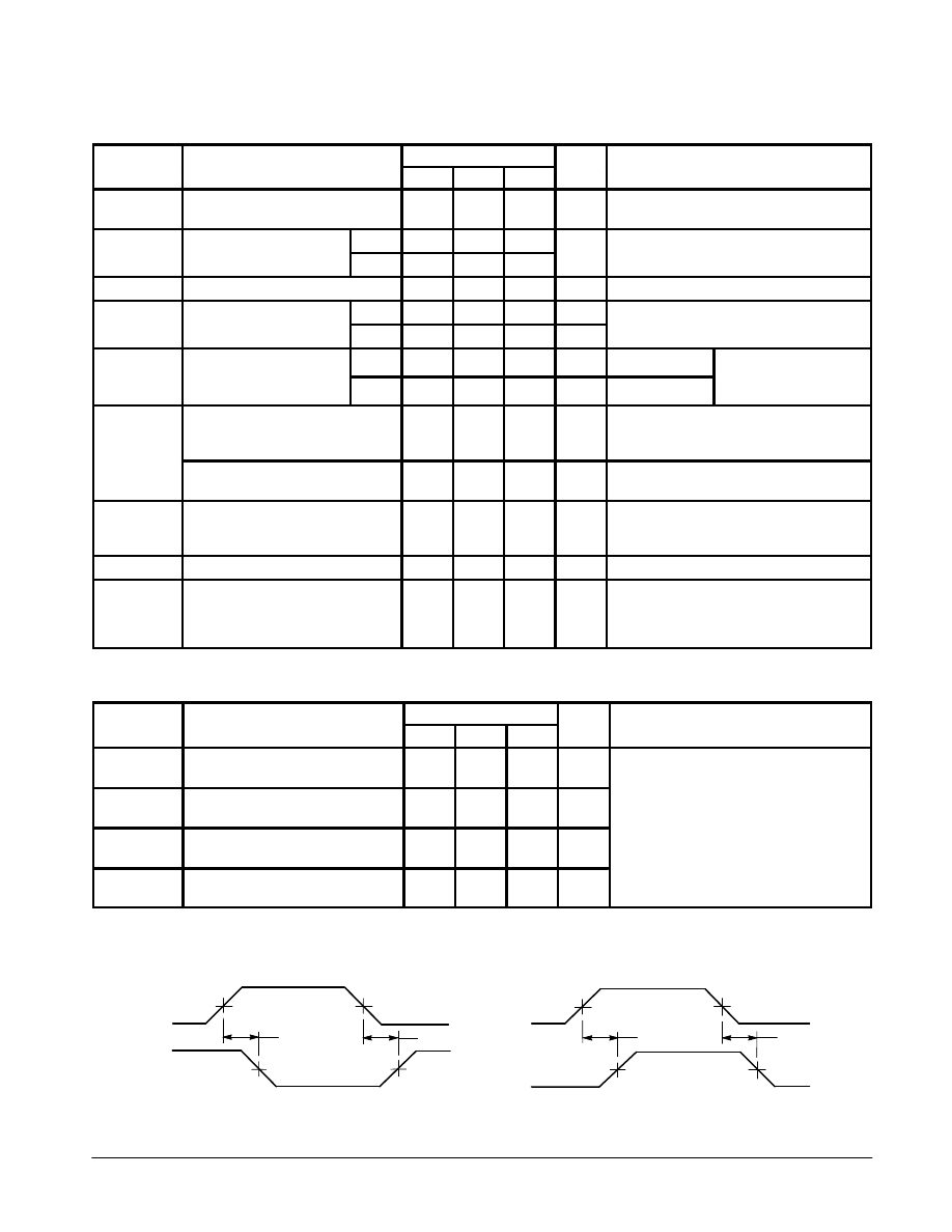
DC CHARACTERISTICS OVER OPERATING TEMPERATURE RANGE
(unless otherwise specified)
Symbol
Parameter
Limits
Unit
Test Conditions
Symbol
Parameter
Min
Typ
Max
Unit
Test Conditions
VIH
Input HIGH Voltage
2.0
V
Guaranteed Input HIGH Voltage for
All Inputs
VIL
Input LOW Voltage
54
0.7
V
Guaranteed Input LOW Voltage for
All Inputs
VIL
Input LOW Voltage
74
0.8
V
Guaranteed Input LOW Voltage for
All Inputs
VIK
Input Clamp Diode Voltage
– 0.65
– 1.5
V
VCC = MIN, IIN = – 18 mA
VOH
Output HIGH Voltage
54
2.5
3.5
V
VCC = MIN, IOH = MAX, VIN = VIH
per Truth Table
VOH
Output HIGH Voltage
54
2.5
3.5
V
VCC = MIN, IOH = MAX, VIN = VIH
per Truth Table
VOH
Output HIGH Voltage
74
2.7
3.5
V
VCC = MIN, IOH = MAX, VIN = VIH
per Truth Table
VOL
Output LOW Voltage
54, 74
0.25
0.4
V
IOL = 4.0 mA
VCC = VCC MIN,
VIN = VIL or VIH
per Truth Table
VOL
Output LOW Voltage
74
0.35
0.5
V
IOL = 8.0 mA
VIN = VIL or VIH
per Truth Table
IIH
Input HIGH Current
C0
A or B
20
40
µ
A
VCC = MAX, VIN = 2.7 V
IIH
C0
A or B
0.1
0.2
mA
VCC = MAX, VIN = 7.0 V
IIL
Input LOW Current
C0
A or B
– 0.4
– 0.8
mA
VCC = MAX, VIN = 0.4 V
IOS
Output Short Circuit Current (Note 1)
– 20
–100
mA
VCC = MAX
ICC
Power Supply Current
All Inputs Grounded
All Inputs at 4.5 V, Except B
All Inputs at 4.5 V
39
34
34
mA
VCC = MAX
Note 1: Not more than one output should be shorted at a time, nor for more than 1 second.
AC CHARACTERISTICS
(TA = 25
°
C)
Symbol
Parameter
Limits
Unit
Test Conditions
Symbol
Parameter
Min
Typ
Max
Unit
Test Conditions
tPLH
tPHL
Propagation Delay, C0 Input
to any
Σ
Output
16
15
24
24
ns
VCC = 5.0 V
CL = 15 pF
Figures 1 and 2
tPLH
tPHL
Propagation Delay, Any A or
B Input to
Σ
Outputs
15
15
24
24
ns
VCC = 5.0 V
CL = 15 pF
Figures 1 and 2
tPLH
tPHL
Propagation Delay, C0 Input
to C4 Output
11
15
17
22
ns
CL = 15 pF
Figures 1 and 2
tPLH
tPHL
Propagation Delay, Any A or
B Input to C4 Output
11
12
17
17
ns
Figure 1
Figure 2
AC WAVEFORMS
VIN
VOUT
1.3 V
tPHL
1.3 V
1.3 V
1.3 V
tPLH
VIN
VOUT
1.3 V
tPLH
1.3 V
1.3 V
1.3 V
tPHL

This datasheet has been download from:
Datasheets for electronics components.
Wyszukiwarka
Podobne podstrony:
Fujifilm X S1 Set To Full Zoom With An
SN7490 DECADE COUNTER DIVIDE BY TWELVE COUNTER 4 BIT BINARY COUNTER
Full Conversations with Millionaires
AT89C51 8 bit Microcontroller with 4K Bytes Flash
AT89C51 8 bit Microcontroller with 4K Bytes Flash
MAKE MONEY FAST WITH FACEBOOK CPALEAD METHOD
2011 Fast accretion of the earth with a late moon froming giant impact Yu
PWR A Full Compensating System for General Loads, Based on a Combination of Thyristor Binary Compens
Damon Brand Magickal Cashbook Attract Money Fast With Ancient Secrets And Modern Wealth Magick Crea
Fast food diet model of NASH with ballooning, progressive fibrosis, and high physiological fidelity
Image Processing with Matlab 33
L 5590 Short Sleeved Dress With Zipper Closure
M 5190 Long dress with a contrast finishing work
O'Reilly How To Build A FreeBSD STABLE Firewall With IPFILTER From The O'Reilly Anthology
więcej podobnych podstron