5-1
FAST AND LS TTL DATA
DECADE COUNTER;
DIVIDE-BY-TWELVE COUNTER;
4-BIT BINARY COUNTER
The SN54 / 74LS90, SN54 / 74LS92 and SN54 / 74LS93 are high-speed
4-bit ripple type counters partitioned into two sections. Each counter has a di-
vide-by-two section and either a divide-by-five (LS90), divide-by-six (LS92) or
divide-by-eight (LS93) section which are triggered by a HIGH-to-LOW transi-
tion on the clock inputs. Each section can be used separately or tied together
(Q to CP) to form BCD, bi-quinary, modulo-12, or modulo-16 counters. All of
the counters have a 2-input gated Master Reset (Clear), and the LS90 also
has a 2-input gated Master Set (Preset 9).
•
Low Power Consumption . . . Typically 45 mW
•
High Count Rates . . . Typically 42 MHz
•
Choice of Counting Modes . . . BCD, Bi-Quinary, Divide-by-Twelve,
Binary
•
Input Clamp Diodes Limit High Speed Termination Effects
PIN NAMES
LOADING (Note a)
HIGH
LOW
CP0
Clock (Active LOW going edge) Input to
÷
2 Section
0.5 U.L.
1.5 U.L.
CP1
Clock (Active LOW going edge) Input to
÷
5 Section (LS90),
÷
6 Section (LS92)
0.5 U.L.
2.0 U.L.
CP1
Clock (Active LOW going edge) Input to
÷
8 Section (LS93)
0.5 U.L.
1.0 U.L.
MR1, MR2
Master Reset (Clear) Inputs
0.5 U.L.
0.25 U.L.
MS1, MS2
Master Set (Preset-9, LS90) Inputs
0.5 U.L.
0.25 U.L.
Q0
Output from
÷
2 Section (Notes b & c)
10 U.L.
5 (2.5) U.L.
Q1, Q2, Q3
Outputs from
÷
5 (LS90),
÷
6 (LS92),
÷
8 (LS93) Sections (Note b)
10 U.L.
5 (2.5) U.L.
NOTES:
a. 1 TTL Unit Load (U.L.) = 40
µ
A HIGH/1.6 mA LOW.
b. The Output LOW drive factor is 2.5 U.L. for Military, (54) and 5 U.L. for commercial (74)
b.
Temperature Ranges.
c. The Q0 Outputs are guaranteed to drive the full fan-out plus the CP1 input of the device.
d. To insure proper operation the rise (tr) and fall time (tf) of the clock must be less than 100 ns.
SN54/74LS90
SN54/74LS92
SN54/74LS93
DECADE COUNTER;
DIVIDE-BY-TWELVE COUNTER;
4-BIT BINARY COUNTER
LOW POWER SCHOTTKY
J SUFFIX
CERAMIC
CASE 632-08
N SUFFIX
PLASTIC
CASE 646-06
14
1
14
1
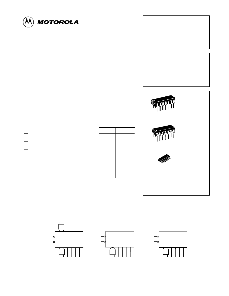
ORDERING INFORMATION
SN54LSXXJ
Ceramic
SN74LSXXN
Plastic
SN74LSXXD
SOIC
14
1
D SUFFIX
SOIC
CASE 751A-02
LOGIC SYMBOL
1 2
2
VCC = PIN 5
GND = PIN 10
NC = PINS 4, 13
VCC = PIN 5
GND = PIN 10
NC = PINS 2, 3, 4, 13
VCC = PIN 5
GND = PIN 10
NC = PIN 4, 6, 7, 13
LS90
LS92
LS93
6 7
1 2
14
1
1 2
2 3
MS
CP0
CP1
MR Q0 Q1 Q2 Q3
12 9 8 11
6 7
14
1
1
CP0
CP1
MR Q0 Q1 Q2 Q3
12
9 8
11
14
1
2 3
CP0
CP1
MR Q0 Q1 Q2 Q3
12 9 8 11
5-2
FAST AND LS TTL DATA
SN54/74LS90
•
SN54/74LS92
•
SN54/74LS93
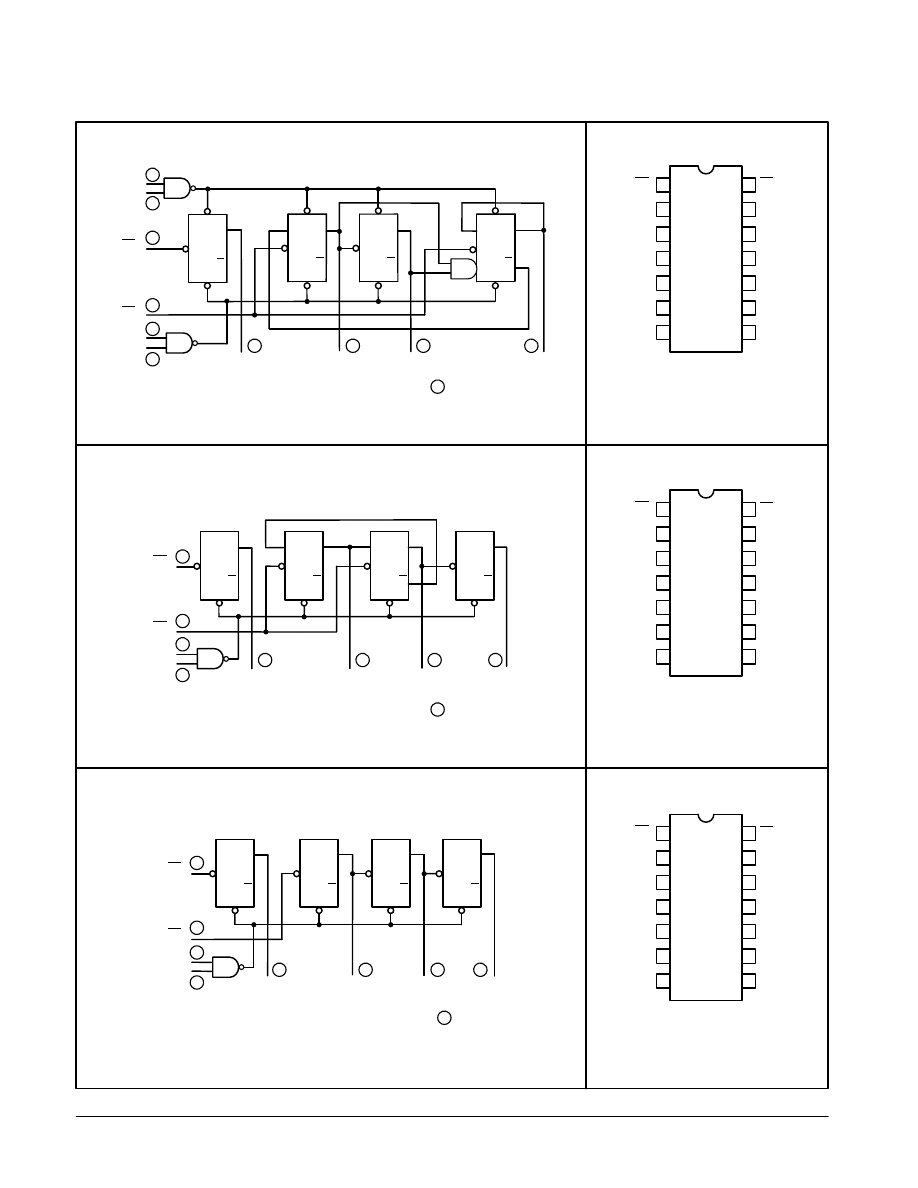
LOGIC DIAGRAM
MS1
MS2
MR1
MR2
CP0
CP1
Q0
Q1
Q2
Q3
MR1
CP0
CP1
Q0
Q1
Q2
Q3
MR2
LS90
MR1
CP0
CP1
Q0
Q1
Q2
Q3
MR2
SD
J
CP
K
Q
Q
CD
SD
R
CP
S
Q
Q
CD
SD
J
CP
K
Q
Q
CD
SD
J
CP
K
Q
Q
CD
J
CP
K
Q
Q
CD
J
CP
K
Q
Q
CD
J
CP
K
Q
Q
CD
J
CP
K
Q
Q
CD
J
CP
K
Q
Q
CD
J
CP
K
Q
Q
CD
J
CP
K
Q
Q
CD
J
CP
K
Q
Q
CD
14
11
12
1
2
6
7
9
3
8
14
13
12
11
10
9
1
2
3
4
5
6
8
7
CP0
NC
Q0
Q3
GND
Q1
Q2
CP1
MR1
MR2
NC
VCC
MS1
MS2
CONNECTION DIAGRAM
DIP (TOP VIEW)
NC = NO INTERNAL CONNECTION
NOTE:
The Flatpak version has the same
pinouts (Connection Diagram) as
the Dual In-Line Package.
14
1
6
7
12
11
9
8
LOGIC DIAGRAM
LS92
14
13
12
11
10
9
1
2
3
4
5
6
8
7
CP0
NC
Q0
Q1
GND
Q2
Q3
CP1
NC
NC
NC
VCC
MR1
MR2
CONNECTION DIAGRAM
DIP (TOP VIEW)
NC = NO INTERNAL CONNECTION
NOTE:
The Flatpak version has the same
pinouts (Connection Diagram) as
the Dual In-Line Package.
LOGIC DIAGRAM
LS93
VCC = PIN 5
GND = PIN 10
= PIN NUMBERS
VCC = PIN 5
GND = PIN 10
= PIN NUMBERS
VCC = PIN 5
GND = PIN 10
= PIN NUMBERS
14
1
2
3
12
9
8
11
14
13
12
11
10
9
1
2
3
4
5
6
8
7
CP0
NC
Q0
Q3
GND
Q1
Q2
CP1
MR1
MR2
NC
VCC
NC
NC
CONNECTION DIAGRAM
DIP (TOP VIEW)
NC = NO INTERNAL CONNECTION
NOTE:
The Flatpak version has the same
pinouts (Connection Diagram) as
the Dual In-Line Package.

5-3
FAST AND LS TTL DATA
SN54/74LS90
•
SN54/74LS92
•
SN54/74LS93
FUNCTIONAL DESCRIPTION
The LS90, LS92, and LS93 are 4-bit ripple type Decade,
Divide-By-Twelve, and Binary Counters respectively. Each
device consists of four master/slave flip-flops which are
internally connected to provide a divide-by-two section and a
divide-by-five (LS90), divide-by-six (LS92), or divide-by-eight
(LS93) section. Each section has a separate clock input which
initiates state changes of the counter on the HIGH-to-LOW
clock transition. State changes of the Q outputs do not occur
simultaneously because of internal ripple delays. Therefore,
decoded output signals are subject to decoding spikes and
should not be used for clocks or strobes. The Q0 output of
each device is designed and specified to drive the rated
fan-out plus the CP1 input of the device.
A gated AND asynchronous Master Reset (MR1
•
MR2) is
provided on all counters which overrides and clocks and
resets (clears) all the flip-flops. A gated AND asynchronous
Master Set (MS1
•
MS2) is provided on the LS90 which
overrides the clocks and the MR inputs and sets the outputs to
nine (HLLH).
Since the output from the divide-by-two section is not
internally connected to the succeeding stages, the devices
may be operated in various counting modes.
LS90
A. BCD Decade (8421) Counter — The CP1 input must be ex-
ternally connected to the Q0 output. The CP0 input receives
the incoming count and a BCD count sequence is pro-
duced.
B. Symmetrical Bi-quinary Divide-By-Ten Counter — The Q3
output must be externally connected to the CP0 input. The
input count is then applied to the CP1 input and a divide-by-
ten square wave is obtained at output Q0.
C. Divide-By-Two and Divide-By-Five Counter — No external
interconnections are required. The first flip-flop is used as a
binary element for the divide-by-two function (CP0 as the
input and Q0 as the output). The CP1 input is used to obtain
binary divide-by-five operation at the Q3 output.
LS92
A. Modulo 12, Divide-By-Twelve Counter — The CP1 input
must be externally connected to the Q0 output. The CP0 in-
put receives the incoming count and Q3 produces a sym-
metrical divide-by-twelve square wave output.
B. Divide-By-Two and Divide-By-Six Counter —No external
interconnections are required. The first flip-flop is used as a
binary element for the divide-by-two function. The CP1 in-
put is used to obtain divide-by-three operation at the Q1
and Q2 outputs and divide-by-six operation at the Q3 out-
put.
LS93
A. 4-Bit Ripple Counter — The output Q0 must be externally
connected to input CP1. The input count pulses are applied
to input CP0. Simultaneous divisions of 2, 4, 8, and 16 are
performed at the Q0, Q1, Q2, and Q3 outputs as shown in
the truth table.
B. 3-Bit Ripple Counter— The input count pulses are applied
to input CP1. Simultaneous frequency divisions of 2, 4, and
8 are available at the Q1, Q2, and Q3 outputs. Independent
use of the first flip-flop is available if the reset function coin-
cides with reset of the 3-bit ripple-through counter.
5-4
FAST AND LS TTL DATA
SN54/74LS90
•
SN54/74LS92
•
SN54/74LS93
LS90
MODE SELECTION
RESET / SET INPUTS
OUTPUTS
MR1 MR2 MS1 MS2
Q0 Q1
Q2 Q3
H
H
X
L
X
L
X
H
H
X
X
L
X
L
L
X
H
L
X
X
L
L
L
H
L
L
L
L
L
L
L
L
H
Count
Count
Count
Count
X
L
H
X
L
L
X
H = HIGH Voltage Level
L = LOW Voltage Level
X = Don’t Care
LS92 AND LS93
MODE SELECTION
RESET
INPUTS
OUTPUTS
MR1 MR2
Q0 Q1
Q2 Q3
H
L
H
L
H
H
L
L
L
L
L
L
Count
Count
Count
H = HIGH Voltage Level
L = LOW Voltage Level
X = Don’t Care
LS90
BCD COUNT SEQUENCE
COUNT
OUTPUT
Q0 Q1
Q2 Q3
0
1
2
3
4
5
6
7
8
9
L
H
L
H
L
H
L
H
L
H
L
L
H
H
L
L
H
H
L
L
L
L
L
L
H
H
H
H
L
L
L
L
L
L
L
L
L
L
H
H
NOTE: Output Q0 is connected to Input
CP1 for BCD count.
LS92
TRUTH TABLE
COUNT
OUTPUT
Q0 Q1
Q2 Q3
0
1
2
3
4
5
6
7
8
9
10
11
L
H
L
H
L
H
L
H
L
H
L
H
L
L
H
H
L
L
L
L
H
H
L
L
L
L
L
L
H
H
L
L
L
L
H
H
L
L
L
L
L
L
H
H
H
H
H
H
NOTE: Output Q0 is connected to Input
CP1.
LS93
TRUTH TABLE
COUNT
OUTPUT
Q0 Q1
Q2 Q3
0
1
2
3
4
5
6
7
8
9
10
11
12
13
14
15
L
H
L
H
L
H
L
H
L
H
L
H
L
H
L
H
L
L
H
H
L
L
H
H
L
L
H
H
L
L
H
H
L
L
L
L
H
H
H
H
L
L
L
L
H
H
H
H
L
L
L
L
L
L
L
L
H
H
H
H
H
H
H
H
NOTE: Output Q0 is connected to Input
CP1.
5-5
FAST AND LS TTL DATA
SN54/74LS90
•
SN54/74LS92
•
SN54/74LS93
GUARANTEED OPERATING RANGES
Symbol
Parameter
Min
Typ
Max
Unit
VCC
Supply Voltage
54
74
4.5
4.75
5.0
5.0
5.5
5.25
V
TA
Operating Ambient Temperature Range
54
74
– 55
0
25
25
125
70
°
C
IOH
Output Current — High
54, 74
– 0.4
mA
IOL
Output Current — Low
54
74
4.0
8.0
mA
DC CHARACTERISTICS OVER OPERATING TEMPERATURE RANGE
(unless otherwise specified)
S
b l
P
Limits
U i
T
C
di i
Symbol
Parameter
Min
Typ
Max
Unit
Test Conditions
VIH
Input HIGH Voltage
2.0
V
Guaranteed Input HIGH Voltage for
All Inputs
VIL
Input LOW Voltage
54
0.7
V
Guaranteed Input LOW Voltage for
VIL
Input LOW Voltage
74
0.8
V
p
g
All Inputs
VIK
Input Clamp Diode Voltage
– 0.65
– 1.5
V
VCC = MIN, IIN = – 18 mA
VOH
Output HIGH Voltage
54
2.5
3.5
V
VCC = MIN, IOH = MAX, VIN = VIH
VOH
Output HIGH Voltage
74
2.7
3.5
V
CC
, OH
,
IN
IH
or VIL per Truth Table
VOL
Output LOW Voltage
54, 74
0.25
0.4
V
IOL = 4.0 mA
VCC = VCC MIN,
VIN = VIL or VIH
VOL
Output LOW Voltage
74
0.35
0.5
V
IOL = 8.0 mA
VIN = VIL or VIH
per Truth Table
IIH
Input HIGH Current
20
µ
A
VCC = MAX, VIN = 2.7 V
IIH
Input HIGH Current
0.1
mA
VCC = MAX, VIN = 7.0 V
IIL
Input LOW Current
MS, MR
CP0
CP1 (LS90, LS92)
CP1 (LS93)
– 0.4
– 2.4
– 3.2
– 1.6
mA
VCC = MAX, VIN = 0.4 V
IOS
Short Circuit Current (Note 1)
– 20
–100
mA
VCC = MAX
ICC
Power Supply Current
15
mA
VCC = MAX
Note 1: Not more than one output should be shorted at a time, nor for more than 1 second.
5-6
FAST AND LS TTL DATA
SN54/74LS90
•
SN54/74LS92
•
SN54/74LS93
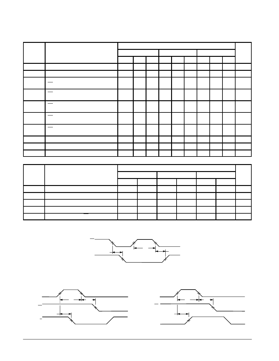
AC CHARACTERISTICS
(TA = 25
°
C, VCC = 5.0 V, CL = 15 pF)
S
b l
P
Limits
U i
S
b l
P
LS90
LS92
LS93
U i
Symbol
Parameter
Min
Typ
Max
Min
Typ
Max
Min
Typ
Max
Unit
fMAX
CP0 Input Clock Frequency
32
32
32
MHz
fMAX
CP1 Input Clock Frequency
16
16
16
MHz
tPLH
tPHL
Propagation Delay,
CP0 Input to Q0 Output
10
12
16
18
10
12
16
18
10
12
16
18
ns
tPLH
tPHL
CP0 Input to Q3 Output
32
34
48
50
32
34
48
50
46
46
70
70
ns
tPLH
tPHL
CP1 Input to Q1 Output
10
14
16
21
10
14
16
21
10
14
16
21
ns
tPLH
tPHL
CP1 Input to Q2 Output
21
23
32
35
10
14
16
21
21
23
32
35
ns
tPLH
tPHL
CP1 Input to Q3 Output
21
23
32
35
21
23
32
35
34
34
51
51
ns
tPLH
MS Input to Q0 and Q3 Outputs
20
30
ns
tPHL
MS Input to Q1 and Q2 Outputs
26
40
ns
tPHL
MR Input to Any Output
26
40
26
40
26
40
ns
AC SETUP REQUIREMENTS
(TA = 25
°
C, VCC = 5.0 V)
S
b l
P
Limits
U i
S
b l
P
LS90
LS92
LS93
U i
Symbol
Parameter
Min
Max
Min
Max
Min
Max
Unit
tW
CP0 Pulse Width
15
15
15
ns
tW
CP1 Pulse Width
30
30
30
ns
tW
MS Pulse Width
15
ns
tW
MR Pulse Width
15
15
15
ns
trec
Recovery Time MR to CP
25
25
25
ns
RECOVERY TIME (trec) is defined as the minimum time required between the end of the reset pulse and the clock transition from HIGH-to-LOW in order to recognize
and transfer HIGH data to the Q outputs
AC WAVEFORMS
Figure 1
Figure 2
Figure 3
*CP
Q
1.3 V
tPHL
tW
1.3 V
1.3 V
1.3 V
1.3 V
tPLH
*The number of Clock Pulses required between the tPHL and tPLH measurements can be determined from the appropriate Truth Tables.
MR & MS
CP
Q
MS
Q0
•
Q3
(LS90)
1.3 V
1.3 V
1.3 V
1.3 V
1.3 V
1.3 V
1.3 V
1.3 V
tPHL
tW
tPLH
trec
tW
CP
trec
Wyszukiwarka
Podobne podstrony:
7490 BINARY and DECADE counter
Healing the Divide by secamimom
Robert Charles Wilson Divided by Infinity
7483 4 BIT BINARY FULL ADDER WITH FAST CARRY
Using Two Part Counterpoint For Non Twelve Tone Music
Comparing the counterpoint books by Jeppesen and Schoenberg
The Making of a Counter Culture Reflections on the Technocratic Society and Its Youthful Opposition
Warhammer 40,000 Horus Heresy 3 Galaxy In Flames (by Ben Counter)
Pathfinder Rise of the Runelords Map Counters
Aleksey Tolstoy Count?gliostro (doc)
Frequency Counter, Layout
serwery do counter strike1 6
easy500 700 Operating hours counter HLP EN
easy500 Counter relay HLP EN
antybiotyki High Speed Countercurrent
Frequency Counter, PCB
Bounce&Countertrend
Klawiszologia Counter Strike
więcej podobnych podstron