
APPLICATION NOTE
Surface mounted triacs and thyristors
Introduction
There is an ever growing need in the electronics
industry for miniaturisation and cost reduction of the
end product. In order to satisfy these requirements,
designers are specifying Surface Mount Technology
with increasing regularity. At first their attentions
were aimed at the low power and small signal
components. Now their attentions are turning towards
the power devices in order to give them total surface
mount solutions.
The increased miniaturisation is possible because
surface mounted power semiconductors occupy less
board area than through-hole-mounting devices on
heatsinks. Cost reduction is possible due to the faster
and simpler assembly that result when ALL
components are surface mounted.
The availability of a wide range of package sizes
permits continuous power dissipations ranging from
0.5 Watts to 2 Watts on standard Printed Circuit
Boards. Higher power dissipations are achievable if
special heatsinking provisions are made on the PCB.
Some examples of these include:
•
A grid of solder vias to a pad on the reverse side
of the PCB.
•
A PCB-mounted heatsink on one or both sides.
•
An aluminium-cored PCB.
•
Fan-assisted cooling.
Surface mount solutions from Philips
Philips Semiconductors has developed a full range of
surface mount power packages for its entire range of
triacs and thyristors. The assembly materials and
technology used are not simply adapted from the
pre-existing through-hole-mounting package
technology; they are unique to SMT.
Every new SMT device is subjected to rigorous
testing which originates from stringent automotive
requirements. This consists of full reliability testing
after three surface mounting operations on printed
circuit boards. No failures will be generated. This
gives the best assurance of reliable end products.
This Technical Publication will present the surface
mount packages and show what thermal
performances can be achieved on standard PCBs
without special heatsinking arrangements.
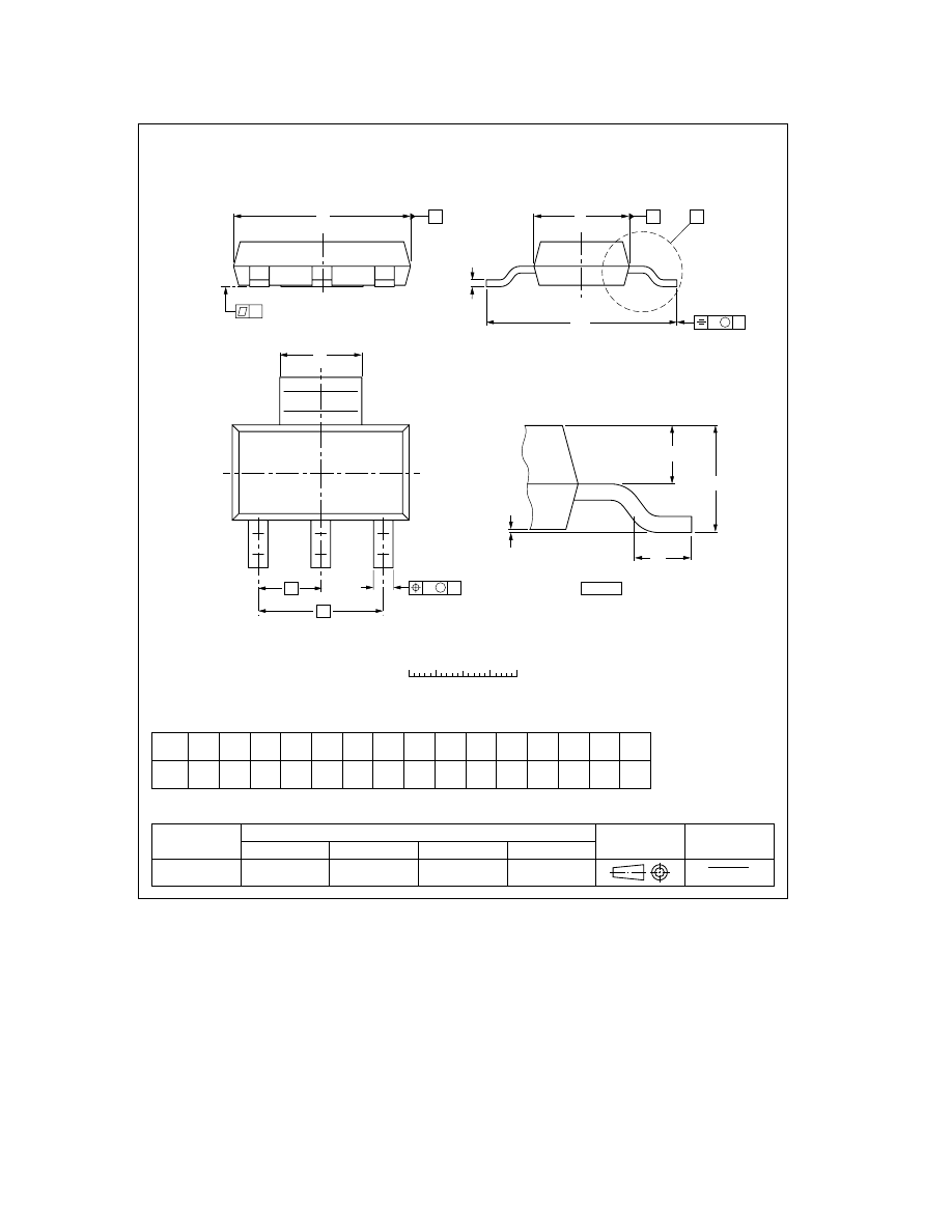
SOT223
SOT223 (Fig. 1) is the smallest SMT power package
presented in this publication. The mechanical design
has been optimised for maximum ease & versatility
of surface mounting, and maximum longterm
reliability in the application. It will provide the
minimum cost of ownership to the Original
Equipment Manufacturer when initial purchase costs,
handling costs and final assembly costs are added
together.
The three legs and the heatsink tab emerge
sideways from the edge of the plastic body, where
they are formed to bring them into contact with the
PCB for soldering to the pads. The centre leg and
the larger heatsink tab on the opposite side of the
package are internally connected.
Because the main tab and the three legs emerge
from the edge of the plastic package and are formed
before they make contact with the PCB, a certain
degree of safe movement of the PCB relative to the
device is possible as the assembly expands and
contracts during soldering and during circuit
operation. Since the device’s diepad is not in direct
and intimate contact with the PCB solder pad,
differential movement caused by different
coefficients of expansion can be accommodated
without excessive fatigue stress to the solder joints.
The more extreme condition of stresses being
transmitted to the die, causing it to crack, is also
minimised with this package design.
SOT223 soldering
When soldering most SMT power packages, a reflow
process must be used. However, for SOT223, it is
also feasible to use wave soldering if required. Wave
soldering is possible because the small size of the
package minimises the size of the “shadow” on the
downstream side of the solder flow. Perhaps more
importantly, the exposed nature of the solder
connections around the periphery of the package,
and their relatively low thermal capacities, mean that
full solder wetting is easily possible with wave
soldering. The good visibility of the solder joints
allows full inspection for quality after assembly.
Figures 2 and 3 show the recommended SOT223
footprints for reflow soldering and for wave soldering.
UNIT
A
1
b
p
c
D
E
e
1
H
E
L
p
Q
y
w
v
REFERENCES
OUTLINE
VERSION
EUROPEAN
PROJECTION
ISSUE DATE
IEC
JEDEC
EIAJ
mm
0.10
0.01
1.8
1.5
0.80
0.60
b
1
3.1
2.9
0.32
0.22
6.7
6.3
3.7
3.3
2.3
e
4.6
7.3
6.7
1.1
0.7
0.95
0.85
0.1
0.1
0.2
DIMENSIONS (mm are the original dimensions)
SOT223
96-11-11
97-02-28
w
M
b
p
D
b
1
e
1
e
A
A
1
L
p
Q
detail X
H
E
E
v
M
A
A
B
B
c
y
0
2
4 mm
scale
A
X
1
3
2
4
Plastic surface mounted package; collector pad for good heat transfer; 4 leads
SOT223
Fig. 1. SOT223.
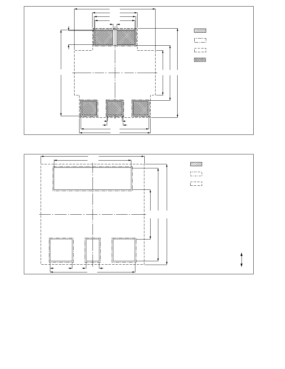
handbook, full pagewidth
MSA443
1.20
(4x)
3.90
5.90
4.80
7.40
4
2
3
1
3.85
1.20 (3x)
1.30 (3x)
,,
,,
,,
,,
,,
,,
,,,,
,,,,
0.30
3.60
3.50
7.00
6.15
7.65
solder lands
solder resist
occupied area
solder paste
Fig. 2. Reflow soldering footprint for SOT223.
handbook, full pagewidth
MSA424
8.70
8.90
7.30
1.90 (2x)
6.70
4
1
2
3
1.10
,,,,,,,
,,,,,,,
,,,,,,,
,,,
,,,
,,,
,,
,,
,,
,,,
,,,
,,,
8.10
4.30
preferred transport direction during soldering
solder lands
solder resist
occupied area
Fig. 3. Wave soldering footprint for SOT223.
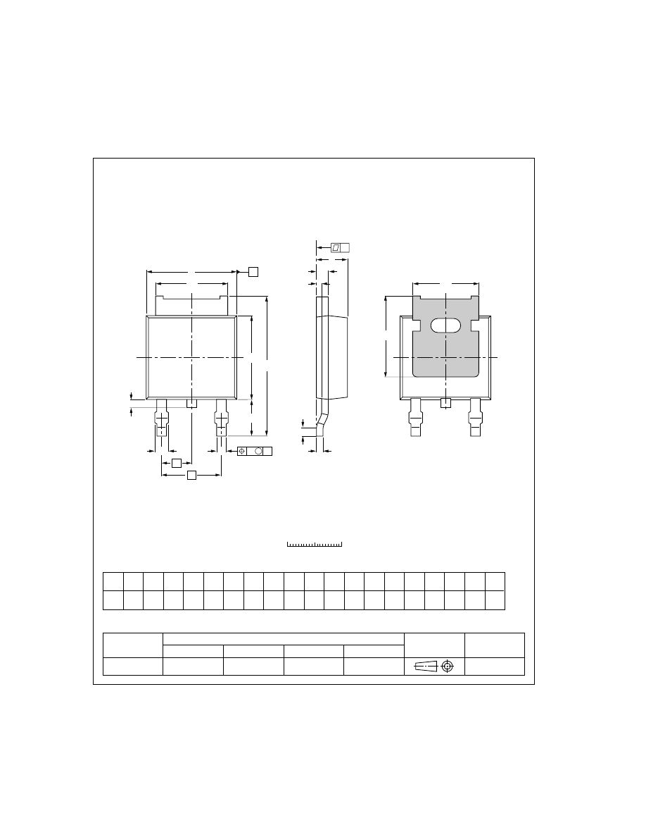
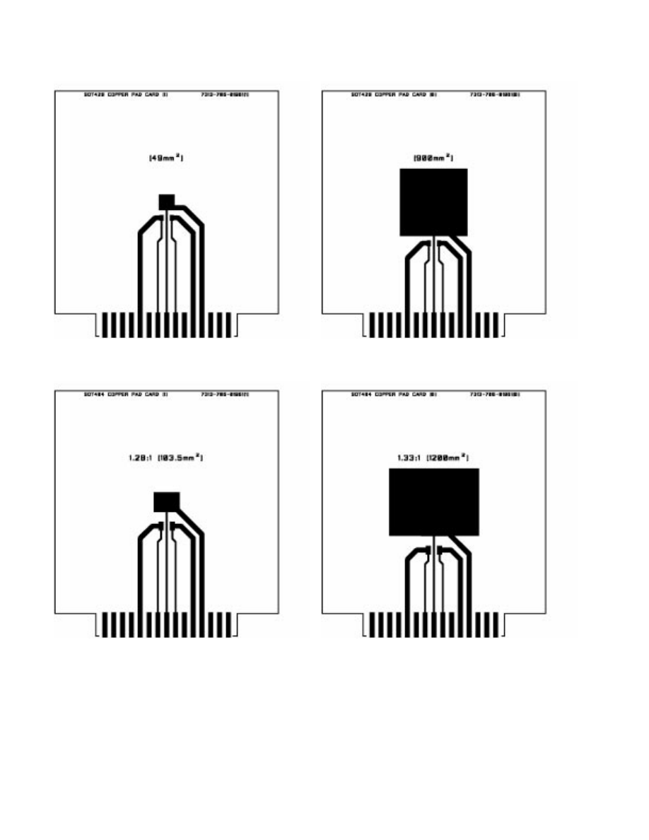
SOT428
SOT428 (also known as TO252 and DPAK) occupies
an area on the PCB which is not much larger than
the area required for SOT223. Indeed, it can be
soldered to a universal SOT223 / SOT428 pad
layout. Figures 5 and 6 show the pad and relative
component sizes. The main pad area of 20mm
2
is
the minimum practical pad size for SOT428.
SOT428 has three legs which emerge from one edge
of the plastic body. The centre leg is cropped off
close to the plastic, so it is not used for electrical
connection. The “centre leg connection” is made
from the device’s metal backplate to the main PCB
pad. The two outer legs are formed to bring them
into contact with the PCB pads for soldering.
REFERENCES
OUTLINE
VERSION
EUROPEAN
PROJECTION
ISSUE DATE
IEC
JEDEC
EIAJ
SOT428
97-06-11
0
10
20 mm
scale
Plastic surface mounted package (Philips version of D-PAK); 2 leads
SOT428
E
b2
D1
w
A
M
b
c
b1
L1
L
1
2
D
E1
HE
L2
Note
1. Measured from heatsink back to lead.
e1
e
A
A2
A
A1
y
seating plane
A1
(1)
D
max.
b
D1
max.
E
max.
HE
max.
w
y
max.
A2
b2
b1
max.
c
E1
min.
e
e1
L1
min.
L2
L
A
max.
UNIT
DIMENSIONS (mm are the original dimensions)
0.2
0.2
mm
2.38
2.22
0.65
0.45
0.89
0.71
0.89
0.71
1.1
0.9
5.36
5.26
0.4
0.2
6.22
5.98
4.81
4.45
2.285
4.57
10.4
9.6
0.5
0.7
0.5
6.73
6.47
4.0
2.95
2.55
Fig. 4. SOT428.
AAAA
AAAA
AAAA
AAAA
AAAA
AAAA
AAAA
AAAA
AAAA
A
A
A
A
A
A
A
A
A
AAAA
AAAA
AAAA
AAAA
AAAA
AAAA
AAAA
AAAA
AAAA
AA
AA
AA
AA
AA
AA
AA
AA
AA
2.3
2.3
1.6 x 3
4.8
4.2
3.0
2.54
AAAA
AAAA
AAAA
AAAA
AAAA
AAAA
AAAA
AAAA
AAAA
AAAA
AAAA
AAAA
AAAA
AAAA
AAAA
AAAA
AAAA
AAAA
AAAA
AAAA
AAAA
AAAA
AAAA
AAAA
AAAA
AAAA
AAAA
AAAA
AAAA
AAAA
AAAA
AAAA
AAAA
AAAA
AAAA
AAAA
AAAA
AAAA
AAAA
AA
AA
AA
AA
AA
AA
AA
AA
AA
AA
AA
AA
AA
AAAA
AAAA
AAAA
AAAA
AAAA
AAAA
AAAA
AAAA
AAAA
A
A
A
A
A
A
A
A
A
Fig. 5. Universal SOT223 / SOT428 pad layout.
Fig. 6. SOT428 & SOT223 relative sizes.
SOT428 soldering
This surface mount package features a relatively
large solder area (compared to SOT223) which is
hidden after assembly. Because the mating surfaces
between the main PCB pad and the device are
remote from the outside world, wave soldering
cannot be relied upon to wet the joint sufficiently. It is
therefore necessary to use a reflow soldering method
for packages of this design. Figure 7 shows the
SOT428 solder pad dimensions.
SOT428 design features for surface mountability
It is well known among power semiconductor
manufacturers that the larger a surface mounted
power semiconductors is, the more vulnerable it is to
die stresses during manufacture and during the
surface mounting process. This can result in a
significant percentage of rejects due to die cracking.
We have learned long ago that it is not possible to
use the same manufacturing techniques for surface
mount devices as are used for through-hole devices.
Unacceptable failure rates will certainly be the result,
either during manufacture, during surface mounting
or during prolonged thermal cycling in the
application.
Philips Semiconductors has spent a long time
perfecting its SOT428 package before releasing it
onto the market so that these pitfalls can be avoided.
Described below are some of the special design
features which ensure successful manufacture and
longterm reliable operation in the customer’s
application.
7.0
7.0
2.15
2.5
4.57
1.5
Fig. 7. SOT428 solder pad dimensions.
1. The package is moulded using a low stress
epoxy plastic in order to minimise the bending
force on the mounting base as curing takes place.
Less bending of the mounting base means less
die stress.
2. A thick copper mounting base of 0.89mm (0.035
inches) max thickness is used to further inhibit
any tendency for bending of the mounting base.
3. A low stress, high lead content soft solder is used
for diebonding. The amount of “give” in the solder
accommodates differential expansions and
minimises die stress.
4. A new technique has been developed to
accurately control the thickness and positioning of
the die-attach solder on the diepad. This
guarantees optimum diebonding over the
complete die area every time without unsoldered
areas or excess solder. The benefit of this is to
offer the best longterm reliability under thermal
stress and the minimum junction-to-mounting
base thermal resistance.
5. Special locking features are used to lock the
epoxy to the metal to improve hermeticity. These
features have been carefully optimised to provide
good hermeticity without locking the epoxy too
rigidly to the diepad, which can result in excess
die stress during differential expansion.
6. A bare copper diepad is used for best adhesion of
the epoxy to the metal. This promotes good
hermeticity.
7. All mating surfaces to be soldered to the PCB
pads are tin-lead solder plated for good
solderability.
8. The footprint is compatible with JEDEC and
Motorola layouts.
9. The coplanarity of leads to seating plane and
leads to leads meets stringent industry standards.
10. A fully automatic high volume production line is
used which takes in the raw components at its
input and delivers assembled, 100% tested,
packaged devices at its output.
11. All assembled devices are subjected to an in-line
surface mount temperature profile pass to
eliminate any remaining possibility, however
small, of zero hour defects at the customer.
12.
Devices are packaged in industry standard blister
pack reels for loading onto automatic pick-and-
place machines.
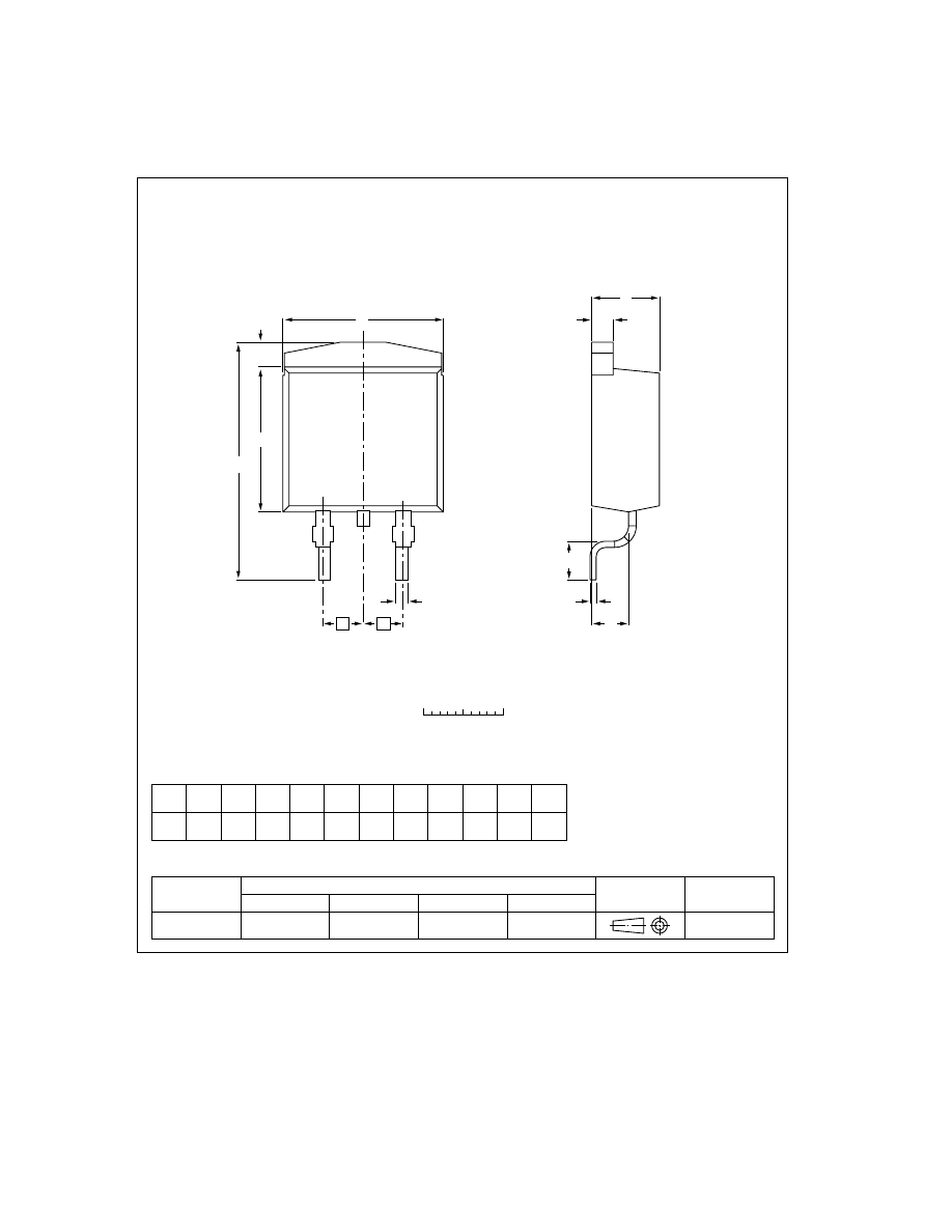
SOT404
SOT404 (Fig. 9, also known as TO263 and D
2
PAK)
possesses the same size of plastic body as SOT78
(TO220). The similarity ends there. SOT404 is
manufactured without a tab since no mounting hole
is required. (It is not merely a cropped TO220!) The
centre lead is cropped close to the plastic, so the
“centre leg connection” is made via the metal
backplate. The two outer leads are formed
downwards to bring them into contact with the PCB.
SOT404 soldering
As for SOT428, it is also not possible to solder
SOT404 using a wave soldering technique. The even
larger body and larger hidden solder area would put
this method out of the question. Reflow soldering is
essential. Figure 8 shows the SOT404 solder pad
dimensions.
SOT404 design features for surface mountability
In designing and manufacturing the SOT404
package, similar measures must be taken as for
SOT428 to ensure a reliable end product. These
include:
17.5
11.5
9.0
5.08
3.8
2.0
Fig. 8. SOT404 solder pad dimensions.
1. A low stress epoxy to minimise bending forces on
the mounting base after curing. (Minimises die
stress.)
2. A thick copper mounting base of 1.4mm (0.055
inches) max thickness to further minimise any
tendency to bend.
3. A low stress, high lead content soft diebond
solder. (Minimises die stress.)
4. Accurate dosing and spreading of the die-attach
solder prior to diebonding to ensure optimum
diebonding over the complete die area every time
without unsoldered areas or excess solder. This
offers best longterm reliability under thermal
cycling and optimum junction-to-mounting base
thermal resistance.
5.
Optimised locking features to balance the
conflicting requirements of good hermeticity with
sufficient differential movement to avoid die
stress fracture.
6. A bare copper comb to ensure good epoxy-to-
metal adhesion for best hermeticity.
7. Tin-lead solder plating of all exposed copper,
including all cropped edges, for optimum
solderability.
8. Compatibility with the industry standard footprint
layout for D
2
PAK.
9. Coplanarity check on leads to seating plane and
leads to leads.
10. A specially designed leadframe to reduce
cropping forces as each device is separated from
the comb. This avoids die cracking due to shock
loading.
11. A surface mount temperature profile pass to
eliminate zero hour defects at the customer.
12. Devices are packaged in industry standard blister
pack reels for loading onto automatic pick-and-
place machines.
UNIT
A
REFERENCES
OUTLINE
VERSION
EUROPEAN
PROJECTION
ISSUE DATE
IEC
JEDEC
EIAJ
mm
A1
D1
D
E
e
Lp
HD
Q
c
2.54
2.60
2.20
15.4
14.8
2.9
2.1
9.65
8.65
1.6
1.2
10.3
9.7
4.5
4.1
1.40
1.27
0.85
0.60
0.64
0.46
b
DIMENSIONS (mm are the original dimensions)
SOT404
97-06-16
0
2.5
5 mm
scale
Plastic single-ended package (Philips version of D2-PAK); 2 leads
SOT404
e
e
E
b
D1
HD
D
Q
Lp
c
A1
A
Fig. 9. SOT404.

Mounting and soldering
The SM footprint drawings define the solder land
(pad) areas, the solder resist areas and the area
occupied by the package. Since the solder lands
must be completely free of solder resist, the areas
without the solder resist are always slighty greater
than the solder land areas. The solder resist must
cover all areas of the PCB that are not soldered to.
This includes extended areas of copper used for
heatsinking.
The footprints for reflow soldering define the solder
paste areas in addition to the areas listed above.
Solder paste is applied using a metal stencil which
must be accurately aligned to within 0.1mm over the
pads. A metal “squeegee” is drawn across the stencil
to deposit the paste through the apertures, which
must be the same size as the solder paste areas
defined on the footprint drawings. With reference to
Figs. 2 & 3, it can be seen that the optimum pad
areas are different for wave soldering and for reflow
soldering.
When wave soldering, surface mount devices must
be held in position by a small measured dose of
adhesive. A double wave process is used to ensure
better wetting of all joints without solder shadows.
Wave soldering must be used if there are any
through-hole components on the PCB.
For reflow soldering, surface mount devices are held
in position by the viscosity of the solder paste. When
the solder is melted in the reflow oven, the surface
tension of the molten solder causes them to self
centre on their pads. For self centreing to operate
reliably, the pad sizes and configuration are critical.
For PCBs which contain a mixture of SM and
through-hole components, both soldering methods
are sometimes employed in order to ensure optimum
soldering of both technologies.
A more detailed description of the wave and reflow
soldering processes is beyond the scope of this
Technical Publication. For a more detailed
description, please see Data Handbook SC18
entitled SMD Footprint Design and Soldering
Guidelines.
Thermal resistance - a laboratory investigation.
Detailed laboratory tests have been conducted on
the junction-to-ambient thermal resistance R
th j-a
of
the SOT223, SOT428 and SOT404 SM packages
when mounted to different pad sizes on standard
FR4 PCB. Sufficient time was devoted to this work to
ensure repeatability of the results and to give a high
level of confidence in their validity.
Theory
It is possible to measure the temperature of a power
semiconductor junction by measuring one of its
temperature-dependent characteristics. For example,
for a MOSFET it might be the forward voltage of the
anti-parallel diode and for a thyristor it would be the
forward voltage drop V
T
. In order to heat up the
device under test, a heating current is passed
through it. When measuring its temperature-
dependent characteristic, a much lower calibration
current is passed for a very short measurement
period. For this investigation, thyristors were used
because of the relative ease of their measurement
and because they were freely available in all the
packages of interest.
The size of the die within any given package will not
affect the final R
th j-a
result appreciably because any
differences in the junction-to-case thermal resistance
R
th j-c
will pale into insignificance compared to the
case-to-ambient thermal resistance R
th c-a
. It is not
critical, therefore, which device is used when
measuring package R
th
in free air or when surface
mounted to conventional PCBs with relatively high
thermal resistances to ambient.
FR4 fibreglass pcb with 35
µ
m copper (1oz/square
foot) was used because it is an industry standard to
which everyone can relate. It is the PCB type which
is always quoted in power semiconductor
manufacturers’ data sheets. It has become a
“reference standard” by default. Despite this
“standard” status, many industries cannot justify its
use because of its cost. The home appliance industry
prefers to use a lower cost alternative, one example
of which is CEM3. This is a resin and paper-based
material with fibre on both sides. Fortunately, the
thermal performance of the cheaper alternatives is
sufficiently close to that of FR4 in many cases to
make the results of this investigation valid for those
also.
Equipment
The test PCBs had pad sizes which varied upwards
from the minimum recommended for the package.
Consistent pad width / height ratios were maintained.
The pad was always positioned centrally on the test
board to assure consistent heatsinking to the bulk of
the PCB. SOT223 and SOT428 used the same pad
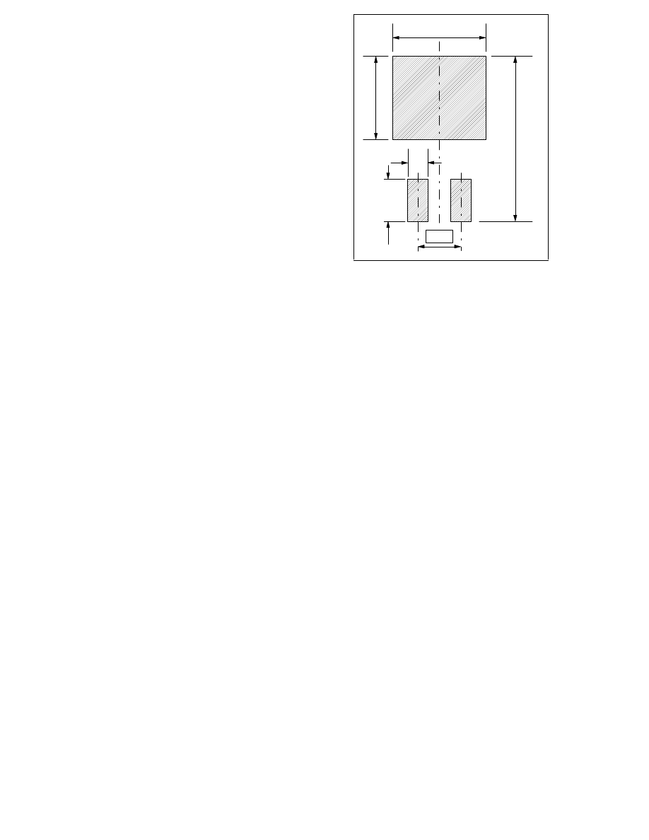
layouts, while SOT404 had its own PCBs. Figure 10
shows the second smallest and largest pad size test
boards for SOT223 / SOT428, and Fig. 11 shows the
smallest and largest pad size test boards for
SOT404. Note that these test boards are not shown
full scale.
Fig. 10. SOT223 / SOT428 test PCB layout, small and large pad areas.
Fig. 11. SOT404 test PCB layout, small and large pad areas.
Separate power and measurement connections were
taken via an edge connector to the device. The
PCBs were standard fibreglass FR4 with 35
µ
m
copper which had been very lightly “tinned” by
electrochemical deposition. (Thermal resistance will
not be reduced by a thick layer of roller tinning!) The
PCBs were made relatively large at 100mm x
100mm to ensure that R
th
is controlled by pad area
and not by PCB area.
Thyristors were tested using a purpose built thermal
resistance test gear. (Thyristors were tested in
preference to triacs because they only require one
measurement for each power setting, whereas triacs
need measuring in both directions with the average
power being calculated from the results.)
The most important fact to remember when
conducting the tests was that they take a lot of time.
It was essential to ensure that thermal equilibrium
and stability had been reached before readings were
taken at elevated device temperature. Rushing the
tests would give incorrect results and improbable
graphs. This was learned from experience.
Results
The resolution and accuracy of the final R
th j-a
results
were maximised by generating high values of
∆
T
j
,
hence large measured
∆
V. The results tables show
R
th j-a
(K/W) versus power dissipation and pad area.
The power levels highlighted by an asterisk indicate
a suggested power dissipation limit for the package
when soldered to the minimum pad area on FR4
PCB. (In the case of the SOT223 package, the
smallest pad area used was 20mm
2
. This area is fully
occupied by the SOT428 package. The minimum for
SOT223 is actually 5.7mm
2
. Therefore the 1W power
dissipation achieved in these experiments will be
higher than that achievable with a 5.7mm
2
pad. 0.5W
is likely to be a practical maximum power dissipation
for SOT223 on a 5.7mm
2
pad.)
The results graphs show R
th j-a
versus pad area and
∆
T
j
versus pad area. For any given package, higher
power dissipation leads to higher
∆
T
j
which leads to
lower R
th j-a
. This is because a larger temperature
difference results in more efficient radiation to
ambient.
SOT223
Area (mm
2
)
0.5W
1.0W*
1.5W
20
110
110
-
49
99
98
-
81
91
90
90
144
88
87
86
256
78
79
78
484
73
74
73
900
68
69
69
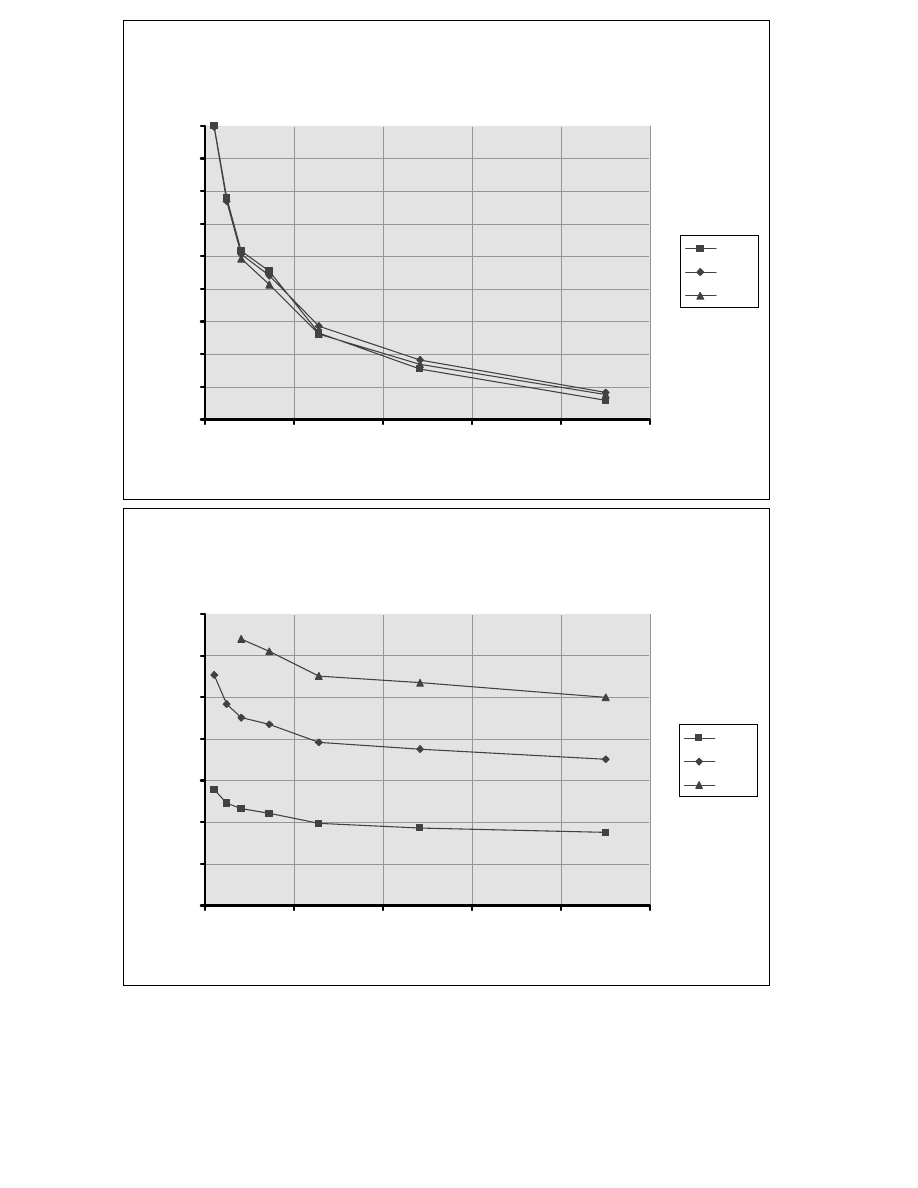
SOT223 Rth j-a vs PCB pad area. 100 x 100 mm FR4 PCB
positioned vertically in still air.
65
70
75
80
85
90
95
100
105
110
0
200
400
600
800
1000
Pad area (sq mm)
Rth j-a (K/W)
0.5W
1W
1.5W
SOT223 Tj rise vs PCB pad area. 100 x 100mm FR4 PCB
positioned vertically in still air.
0
20
40
60
80
100
120
140
0
200
400
600
800
1000
Pad area (sq mm)
Delta Tj (deg C)
0.5W
1W
1.5W
SOT428
Area (mm
2
)
0.5W
1.0W*
1.5W*
2.0W
2.5W
3.0W
20
90
85
-
-
-
-
49
77
75
73
72
-
-
81
71
69
66
65
-
-
144
64
62
60
59
58
-
256
58
56
54
53
52
-
484
54
50
48
47
46
45
900
46
45
43
43
42
41
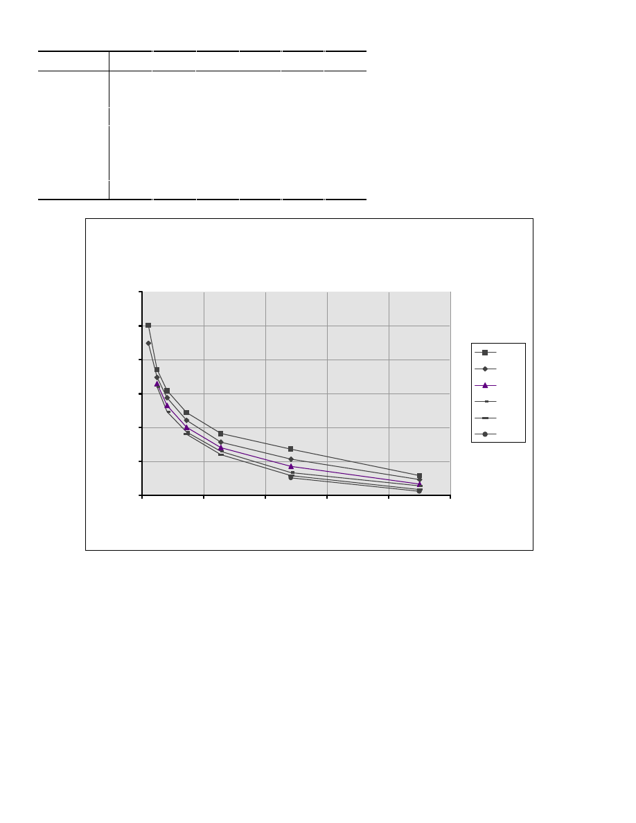
SOT428 Rth j-a vs PCB pad area. 100 x 100 mm FR4 PCB
positioned vertically in still air.
40
50
60
70
80
90
100
0
200
400
600
800
1000
Pad area (sq mm)
Rth j-a (K/W)
0.5W
1W
1.5W
2W
2.5W
3W
SOT428 Tj rise vs PCB pad area. 100 x 100mm FR4 PCB
positioned vertically in still air.
0
20
40
60
80
100
120
140
160
0
200
400
600
800
1000
Pad area (sq mm)
Delta Tj (deg C)
0.5W
1W
1.5W
2W
2.5W
3W
SOT404
Area (mm
2
)
1.0W
2.0W*
3.0W
103.5
60
55
-
192
52
47
-
300
47
43
41
475
41
39
37
825
39
36
34
1200
36
34
32
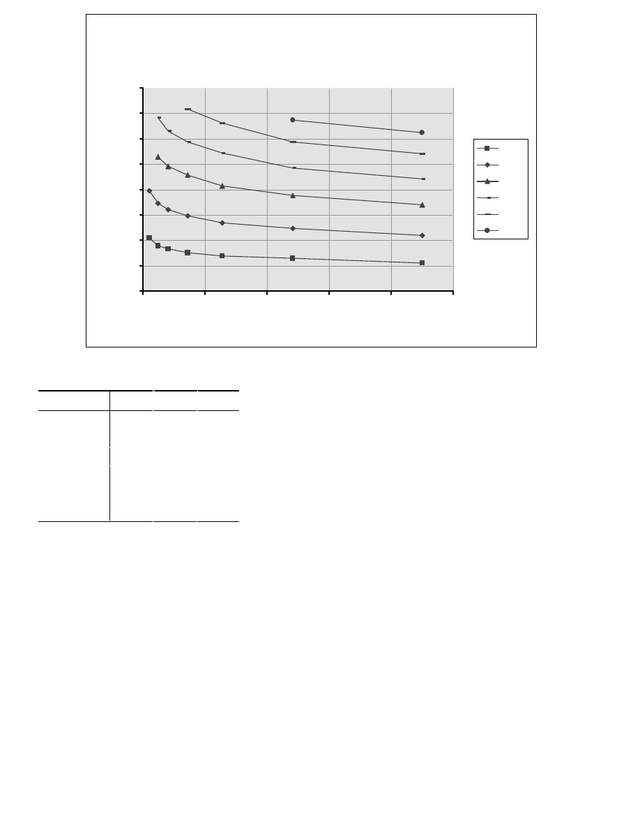
SOT404 Rth j-a vs PCB pad area. 100 x 100mm FR4 PCB
positioned vertically in still air.
30
35
40
45
50
55
60
0
200
400
600
800
1000
1200
Pad area (sq mm)
Rth j-a (K/W)
1W
2W
3W
SOT404 Tj vs PCB pad area. 100 x 100mm FR4 PCB
positioned vertically in still air.
0
20
40
60
80
100
120
140
0
200
400
600
800
1000
1200
Pad area (sq mm)
Delta Tj (deg C)
1W
2W
3W
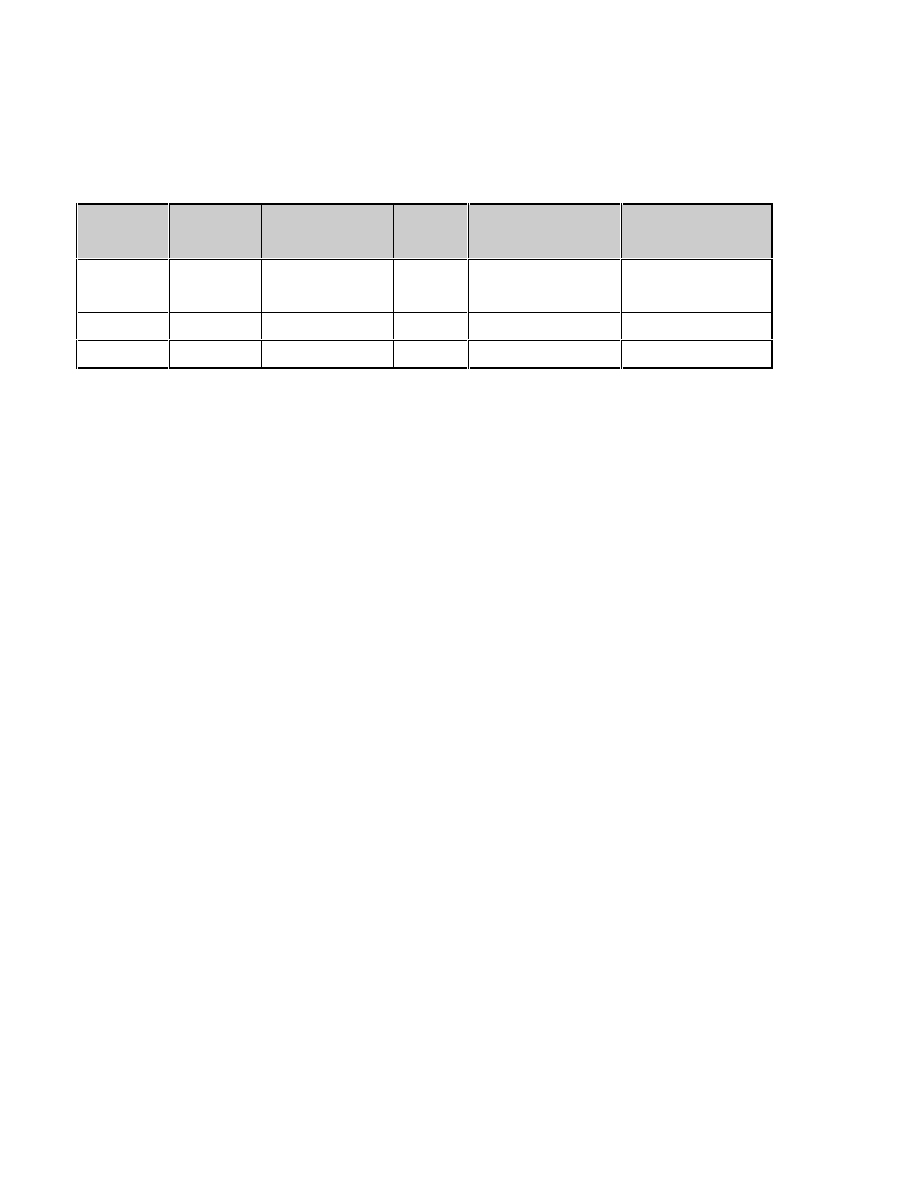
Conclusions
The maximum practical power dissipations are
summarised below for stagnant ambient conditions
at 25
°
C. These are for standard FR4 PCB or similar
without special heatsinking provisions. The 35
µ
m
copper had been lightly tinned by electrochemical
deposition.
SOT223 and SOT428 can be soldered to common
pad layouts. 20mm
2
was the absolute minimum pad
area for soldering SOT428. A reasonable power
dissipation for SOT428 on 20mm
2
fell somewhere
between 1.0W and 1.5W.
The minimum pad quoted in data for SOT223 is
5.7mm
2
. 0.5W is a more realistic maximum power
dissipation for SOT223 on its minimum pad.
Package
Pmax (W)
Pad area (mm
2
)
∆
T
j
(
o
C)
R
th j-a
(K/W)
R
th j-a
(K/W)
(experimental)
(quoted in data)
SOT223
1.0
20
650
97
74
99
72
156 (5.7mm
2
pad)
70 (648mm
2
pad)
SOT428
1.0<1.5
20
106
73
75
SOT404
2.0
104
108
55
55
Naked dice
All Philips’ thyristors and triacs can be supplied as
naked dice if required. Please contact your local
sales office for details.
Document Outline
- Introduction
- Surface mount solutions from Philips
- SOT223
- SOT428
- SOT404
- Mounting and soldering
- Thermal resistance - a laboratory investigation.
Wyszukiwarka
Podobne podstrony:
Power Amplifiers With Valves An Approach And A Practical Circuit (Claus Byrith)
Prosecuting Computer Virus Authors The Need for an Adequate and Immediate International Solution
Build an Arts and Crafts Bookcase
A worldwide geographical distribution of the neurotropic fungi, an analysis and discussion (Gastón G
Kitayama, Duffy, Kawamura Perceiving an Object and its Con
John Tietz An Outline and Study Guide to Heidegger Being and time
an alternative and simple preparation of tryptamine from l tryptophan by catalytic decarboxylation w
What Is an Apparatus and Other Essays Giorgio Agamben
Polish Literature in 1864 1914 an End and Beginning
Poland, 1918 1945, An Interpretive and Documentary History of the Second Republic
Analysis of soil fertility and its anomalies using an objective model
How does personality matter in marriage An examination of trait anxiety, interpersonal negativity, a
an essay?out this and that 4N3M6QTFCETLGHNHFCD7NMYUIU5DWJRSCGSGEJY
21 269 287 Effect of Niobium and Vanadium as an Alloying Elements in Tool Steels
Britain and Europe an uneasy relationship
P4 explain how an individual?n exercise command and control
więcej podobnych podstron