87805 ST Z11 15
■ SCHEMATIC DIAGRAM
(This schematic diagram may be modified at any time with the development of new technology.}
Notw:
|
Lch |
1 |
S1-2,1-2 |
FM muting/FM modę selector switch in "on/FM auto" position. |
|
on/FM auto -—► off/FM mono | |||
|
OUTPUT |
2. |
S2-1 : |
Band selector switch in "FM" position. |
|
R ch |
3. |
S3-1,3-2 |
r lvl oiyi : FM IF-band selector switch in "normal" position. |
|
4. |
S6 : |
norrnal —- super narrow Voltage selector switch in "240V" position. © 110V—* ®120V-—*■ (5) 220V ---- © 240V | |
|
5. |
SB |
Power switch in "on" position. | |
|
6. |
Indicatcd |
voltage values are the standard values for the unit measured by the DC |
electronic Circuit tester fhigh-impedance) with the chassis taken as standard. Therefore. there may exist some errors in the voltage values, depending on the internal impedance ot the DC Circuit tester.
* Figures in t lstand for DC voltaga in FM/AM signal reception modę.
* Figures in < >stand for DC voltage In FM stereo signal reception modę.
* Figures in r jstand for DC voltage in FM Ino signsl) muting to on modę.
* Figures in ( )stand for DC voltage with the bsnd selectors Circuit set at AM.
7. Signal lines
1 0 FM signal Positive (+8) voltage linę
Audio frequency signal AM signal
8. Important safety notice:
Components identified by A make have special characteristics important for safety. When replacing any of these components, use only manufacturer's specified parts.
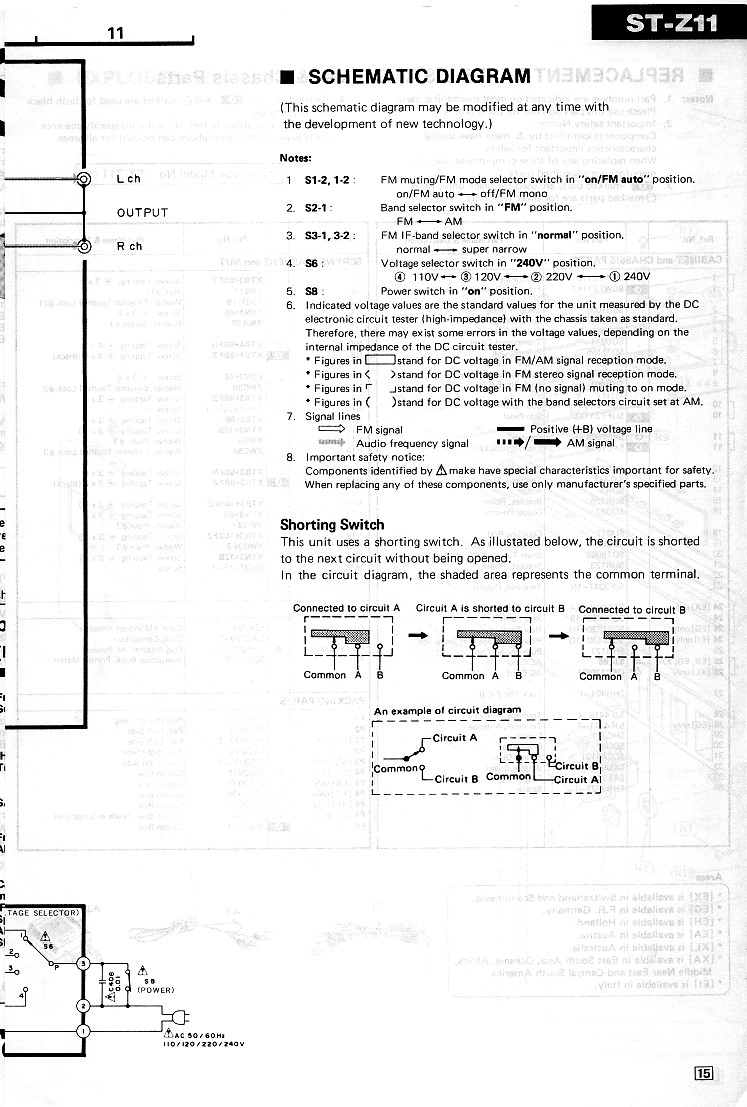
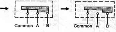
Shorting Switch
This unit uses a shorting switch. As illustated below, the Circuit is shorted to the next Circuit without being opened.
In the Circuit diagram, the shaded area represents the common terminal.
Connected to Circuit A r-------1
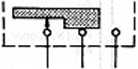
Common A 8
Circuit A is shoriod to Circuit B Connected to Circuit B

An example of Circuit diagram (—Circuit A (---
ircuit B, ircuit Al
____I
Common o T :ircui
1— Circuit B Common
Wyszukiwarka
Podobne podstrony:
ST Z11 10 ST-Z11■ BŁOCK DIAGRAM S2 IBond selcctor) VR30l(FM MPX V.CO.
36509 ST Z11 10 ST-Z11■ BŁOCK DIAGRAM S2 IBond selcctor) VR30l(FM MPX V.CO.
36509 ST Z11 10 ST-Z11■ BŁOCK DIAGRAM S2 IBond selcctor) VR30l(FM MPX V.CO.
Follow this w i ring diagram when assembling the PCB. Take care with the orientation of the capacito
-9 Rys. 3. Schemat pomiaru metodą dwusiecznych jednego poziomu z jednego stanowiska Fig. 3. The sche
Entrelac Patterns This child s sweater can be worked in any size. The diagram shows the differe
(c) Explain the working of DVD-ROM with the hełp of błock diagram. 4 5.
ST Z11 11 ST-Z11■ CIRCUIT BOARDS AND WIRING CONNECTION DIAGRAM — i-- SVI/jPC I0I8C FM A
25295 ST Z11 11 ST-Z11■ CIRCUIT BOARDS AND WIRING CONNECTION DIAGRAM — i-- SVI/jPC I0I8C FM A
25295 ST Z11 11 ST-Z11■ CIRCUIT BOARDS AND WIRING CONNECTION DIAGRAM — i-- SVI/jPC I0I8C FM A
ST Z11 02 ST-Z11 Deutsch TECHNISCHE DATEN (DIN 45 500) (Spezifikationen kónnen infolge von Verbe$ser
ST Z11 03 ST-Z11■ LOCATION OF CONTROLS — FM stereo indicator N —Signal-strength indicators Power Ban
ST Z11 05 -ST-Z11 AM/FM SIGNAL GENERATOR CONNECTION FREOUENCY DIAL SETTING INDICATOR (VTVM or
ST Z11 06 ST-Z11 AM/UKW MESSENGER SKALENZEI-GEREIN-STELLUNG DES TUNER ANZEIGEGEIRAT <Rohrenvolt
więcej podobnych podstron