And the Survc
MA
says.
.NAGER
n our business, when someone talks about
collecting data, we immediately start coming up
with solutions for how we’re going to collect the data.
Battery operation, low-power sleep mode, wake-up timers,
nonvolatile memory..
list goes on. However,
it comes
to
laying out the task, what we collect and what we do with it inevitably
overshadows how we do it.
We recently conducted a survey of a random sampling of Circuit Cellar
The “how” was obvious: mail a sheet of paper to a list of names
and wait for the results to come back. The “what” was a whole lot more
difficult, and we spent many hours coming up with questions for the survey.
Once the raw data had come in, though, the task grew in size again.
How do you meaningfully compile, combine, and interpret the results into
something useful? It’s far too easy to skew the numbers or compare apples
with oranges and end up with meaningless answers.
After going through all these convolutions, what did we find? It turns
out we know our readers pretty well, and most approve of what we’re doing.
For more information on some of what we learned about you, the reader,
turn to Priority Interrupt and read what Steve has to say.
Moving from the
back to the “how,” Damon Chu starts this Data
Acquisition issue with a look at the newest members of the PIC family and
how they are ideally suited to many low-power data-acquisition systems.
Next, Steven Kraft helps out a hard-of-hearing grandmother with a
messaging device that works with ordinary phone lines using DTMF and
without complicated equipment.
Craig Pataky next takes us on a trip through a
to connect
stalwart DOS code with a flashy Windows 95 front end. The result is reliable,
well-tested code that meets the expectations of today’s desktop user.
Finally, Bill Jackson and Reynaldo
show how a RISC
processor can be superreduced, resulting in an even smaller instruction set
and faster speeds.
In our columns, lngo Cyliax continues the development of his
MC68030 trainer board by going over the monitor and boot code. The board
even boots over a network. Jeff explores the latest in low-cost prototype PC
boards and finds the days of point-to-point wiring and wire-wrapping are
drawing to a close. Lastly, Tom strolls into the analog camp again with a new
programmable analog array device.
Embedded
starts this month with Jim Blazer, Janos Levendovszky,
and Robert Haris describing a distributed approach to data acquisition. It lets
the main processor do the real computing, while the chores of collecting the
data are handled by another processor. Steve Lisberger follows suit by
unveiling a design that times events with microsecond precision and minimal
impact on the main processor.
In the
Dennis Liles and Rick Lehrbaum introduce EBX,
a new open standard in high-power, compact, embeddable form factors.
Fred Eady wraps up his NASA plant-growth chamber with a look at remotely
collecting data and displaying it over the Internet.
CIRCUIT
T H E C O M P U T E R A P P L I C A T I O N S J O U R N A L
EDITORIAL DIRECTOR/PUBLISHER
Steve Ciarcia
EDITOR-IN-CHIEF
Ken Davidson
MANAGING EDITOR
Janice Hughes
TECHNICAL EDITOR
Elizabeth
ENGINEERING STAFF
Jeff Bachiochi
WEST COAST EDITOR
Tom Cantrell
ASSOCIATE PUBLISHER
Sue Hodge
Rose
CIRCULATION CONSULTANT
John Treworgy
BUSINESS MANAGER
Jeannette Walters
ADVERTISING COORDINATOR
Valerie Luster
CONTRIBUTING EDITORS
Rick Lehrbaum
Fred Eady
NEW PRODUCTS EDITOR
Weiner
ART DIRECTOR
KC
PRODUCTION STAFF
John Gorsky
James Soussounis
CIRCUIT CELLAR
THE COMPUTER
JOURNAL (ISSN 0696.6965) is published
monthly by Circuit Cellar Incorporated, 4 Park Street,
CT06066
Periodical
rates paid at Vernon, CT and additional offices.
year (12 issues) subscription rate U.S.A. and posses-
$21.95, Canada/Mexico $31.95, all other
tries $49.95. All subscription orders payable in U.S.
funds
via international postal money order or
check drawn on US bank.
VISIT OUR WEB SITE FOR SUBSCRIPTION
AT
subscription orders and subscription
questions to
Cellar INK Subscriptions, P.O.
POSTMASTER: Please send address changes to
Holmes,
PA 19043.9613.
Cover photograph Ron Meadows Meadows Marketing
PRINTED IN THE UNITED STATES
For information on authorized reprints of articles,
contact Jeannette Walters (660) 675-2199.
ASSOCIATES
NATIONAL ADVERTISING REPRESENTATIVES
NORTHEAST
MIDWEST SOUTHEAST
WEST COAST
MID-ATLANTIC
Collins
Barbara Jones
Barbara (Best)
(954) 966-3939
&Shelley Rainey
(561) 694-2044
Fax: (954) 965-6457
(714) 540-3554
Fax: (561)
Fax: (714) 540-7103
Circuit Cellar
bps, 6 bits, no parity, 1 stop bit,
671-1966. For
mall to
World Wide Web:
All programs and schematics in
Circuit Cellar
have been
reviewed to ensure their performance is
inaccordance with
transfer by subscribers.
programs schematics or for the consequences of any such errors. Furthermore, because of possible variation
the quality and condition materials and workmanship of reader-assembled
Circuit Cellar
disclaims any
for the safe and proper
of reader-assembled projects based upon or from
plans, descriptions, or information published in
Cellar
Entire contents copyright 1997 by Circuit Cellar Incorporated. All
reserved.
Circuit Cellar
a
registered trademark of Circuit Cellar Inc. Reproduction of this publication in whole or in
without written
consent from Circuit Cellar
is
2
Issue
97 October 1997
Circuit Cellar INK@
12
18
q
From the Bench
And the Survey Says...
Prototypes of the Rich and Famous-Not!
Bachiochi
Reader
q
Silicon Update
New
Product News
of Analog Hope
Tom Cantrell
edited by Harv Weiner
Advertiser’s Index
Analog Data Acquisition
Damon Chu
DTMF Message Decoders
Telephone Aids for the Hearing Impaired
Steven Kraft
Interprocess Communication
Moving DOS Programs into Windows
Craig Pa taky
Compressed-Code
Bill Jackson Reynaldo
q
MC68030
Workstation
Part 2: The Boot PROM Monitor Device Drivers
Cyliax
Task Manager
Ken Davidson
30
N o u v e a u P C
edited by Harv Weiner
Intelligent Data Acquisition
Blazer,
Levendovszky,
Robert Haris
Precision Timing and I/O
Steve Lisberger
Quarter
Steps Out of the Box
60
Applied
P C S
Managing a NASA Plant-Growth Chamber
Part 2: Coordinating Sensors and Analyzing Data
Fred Eady
Dennis
Rick Lehrbaum
Circuit Cellar
Issue 87 October 1997
3
OTHER ANGLES ON THE REMOTE EDGE
Daniel
and Michael Miller’s “A Universal IR
Remote-Control Receiver” (INK 82) was very useful. I’m
building a TV remote by adding an IR LED and
to an old calculator. Since the calculator has a spare slide
switch, I’m including my NEC VCR’s functions. I mea-
sured NEC and
remote codes with a photodiode
and amplifier connected to a bit on a PC printer port.
My NEC-remote code patterns agreed exactly with the
timing values in the article. So, I was surprised that Joe
(Reader I/O, INK 85) claims the NEC chip sends
two code patterns per key press. I did not observe this.
I think the remote’s “repeat” function is the issue. If a
key is pressed and held down, each remote continuously
sends a train of codes at 10 codes per second (100 ms
between sync pulses). The
remote repeats the
same code until the key is released.
On the NEC remote, the first code sent is the unique
key code described in the article. All remaining codes
sent are a fixed, nonstandard code that’s the same for all
keys and apparently means “repeat the last command.”
The code is nonstandard because it doesn’t have the
normal off time following the sync pulse.
The repeat code is: 9 ms on, 2.3 ms off, 0.6 ms on, no
additional bits following. The interval between the end
of the first code and the beginning of the repeat code is
100 ms (length of key code). Since each bit in the key
code is also transmitted as its complement, all bits take
the same time to send (1.2 + 2.3 = 3.5 ms). The key-code
length is then: 9 + 4.5 +
= 69.5, leaving a
interval. The repeat period is a nominal 100 ms but was
observed to be 104 and 108 ms in the two remotes, so Mr.
value of 40 is consistent with normal variations.
I also saw the stop pulse he refers to and originally
interpreted it the same way he did. But, if bits are on
times followed by off times, then a final stop pulse is
needed to terminate the last off time.
But, suppose a bit is a variable off time followed by a
fixed on time. The code sequence is: sync pulse (long on),
mode pulse (long off followed by the first
on pulse),
then 32 bits (off followed by on). The final on pulse is part
of the last bit. Now, the mode bit distinguishes a normal
data word (4.5 ms off) from a repeat code (2.3 ms off].
John N. Power
CA D PA K
Windows-$199, DOS
Ideal for New Users, Hobbyists, Small Businesses!
Provides everthing for PCB Layout Schematic Drawing
P R O T E U S
Most Powerful EDS System on the market!!!
Schematic Capature Circuit Simulation
l
PCB Layout
Rip-Up Retry Autorouting
R4
S Y S T E M S I N C .
1100
ST.
N E W M A R K E T O N T A R I O
FREE DEMO
CANADA
0
WRITE OR CALL
905
FAX 905
TO DAY
905
ALL POINTS BULLETIN !!
BE ON ALERT FOR THE
LOWER COST, FASTER, EASIER TO PROGRAM SINGLE CHIP COMPUTER
COMPARE:
DEM
PROGRAM DOWNLOAD NO
YES
CHIP OPERATION NO
YES
BUILT-IN BASIC
NO
YES
EEPROM DATA MEMORY NONE
64
PROGRAM MEMORY
768 OTP
FLASH
MATH REGISTERS
1
32
MAX INSTRUCTIONS/SEC
ZOM
MAX COUNTER BITS
16
18
INPUT/OUTPUT BITS
12
15
TO D COMPARATOR
NO
YES
HARDWARE INTERRUPTS NONE
3
PIC IS A REGISTERED TRADEMARK OF
RESET
PDO 2 19
3 18
XOUT 4 17
XIN 5 16
6 15
PD3 7 14
1 3
PD5 9 12
GND 10 11
PB7
PB6
PB5
PB4
PB3
PB2
PD6
CREDIT CARD
COMPUTER
EVAL KIT $75.00
PROGRAM DOWNLOAD
NONVOLATILE MEM.
-LCD/KEYPAD INTERFACE
-ISA BUS (MODEM,MEM,ETC.)
SERIAL TO
-ASSEMBLY/BUILT-IN BASIC
-100
OPERATION
6
Issue 87 October
1997
Circuit Cellar INK@
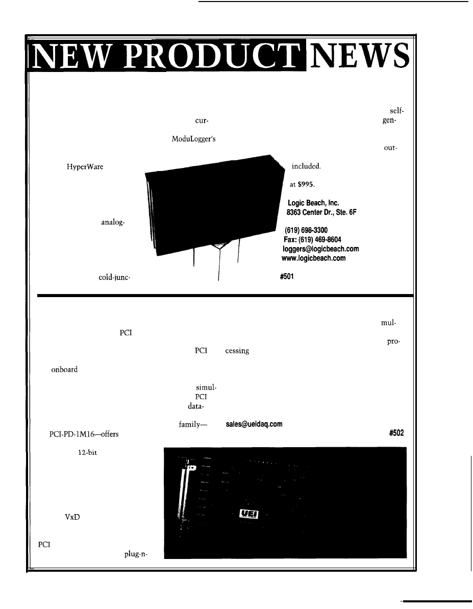
Edited by Harv Weiner
DATA LOGGING SYSTEM
The
ModuLogger
is a battery-powered, self-contained
tion compensation for thermocouple applications. A
portable data-logging and alarming system designed for
self-calibration feature includes user-programmable
sampling and storing flow, pressure, temperature,
calibration cycles. A single software-configurable
rent, power, and other process, vehicle, and utility signal
eral-purpose digital input logs events or counts digital
data over time. After on-site collection, the
outputs from flow meters, encoders, or other pulse-train
memory can be serially downloaded via modem
sources. Isolated alarm relay
or RS-232 link to a PC. With the
puts and a TTL alarm output are
provided
for Win-
dows software, data can be
The ModuLogger system starts
further manipulated, plotted,
and/or converted to various
spreadsheet formats.
The ModuLogger accepts
up to four universal
type inputs, which are soft-
ware configurable for six
thermocouple types, 15 ranges
of DC voltage, or seven ranges
of DC current. Another analog
channel is used for
La
Mesa, CA 91942
DATA-ACQUISITION CARD
UEI has introduced a family of data-acquisition cards
play support, bus-mastering block data transfers,
featuring the
PowerDAQ
interface. PowerDAQ is a
tiple simultaneous command requests from concurrent
DSP-enhanced PCI-interface subsystem incorporating a
Win32 application threads, and concurrent request
Motorola DSP56301 processor with an integrated
(multiprocessor systems).
controller linked via internal data bus to system logic
Pricing for the PowerDAQ starts at $1650.
and
memory. Because the PowerDAQ interface
functions as a multithreaded processor, a fatal error in
United Electronic Industries, Inc.
one process does not terminate operations running
10 Dexter Ave.
taneously. This interface transfers data across the
Watertown, MA 02172
bus at rates of 132 MHz-much faster than the
(617) 924-1155
acquisition card’s maximum sampling speed.
Fax: (617) 924-1441
The first member of this data-acquisition
the
16 single-ended analog input
www.ueidaq.com
channels sampling (continuously) at
1 MHz with
resolution, two
12-bit analog output channels, eight
high-speed digital input lines, eight
high-speed digital output lines, and
three user-accessible counter/timers.
Each PowerDAQ card comes with
a set of UEIDAQ software that in-
cludes a
for Windows 95 and
kernel-mode drivers for Windows NT.
These drivers support all relevant
features, including PCI-bus
PowerDAQ detection, true
8
Issue 87 October 1997
Circuit Cellar INK@
I
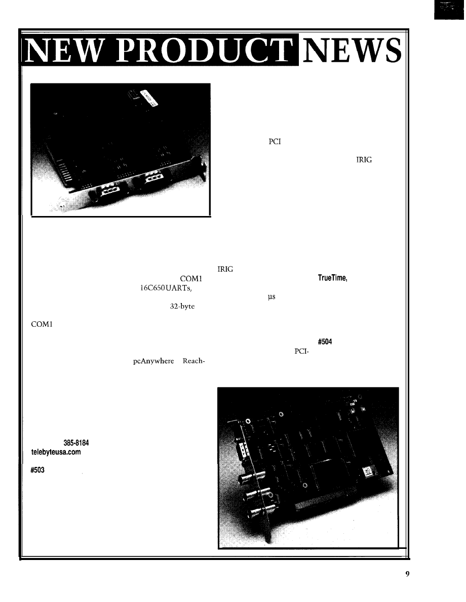
ULTRA-HIGH-SPEED PC COM PORT
The Telebyte Model 480 dual-port, ultra-high-speed
serial-I/O card enables high-speed serial data connectiv-
ity for ISDN and other technologies. The card can be
used in either ISA- or EISA-bus-based PC systems in
any application where the standard speed from
or COM2 is insufficient. By using
the
Model 480 can support speeds up to 460 kbps on both
serial ports. System overhead is reduced via
buffers. The card can be mapped to any location from
to COM4 and use standard COM port drivers.
Custom drivers are supplied to get the full benefit of the
available performance.
Using the Model 480 in combination with software
communications packages (e.g.,
or
Out), users can effectively access a remote PC and per-
form tasks on the remote machine as if it were a local
PC. The card sells for $79.
Telebyte Technology, inc.
270 Pulaski Rd.
Greenlawn, NY 11740-1616
(516) 423-3232
Fax: (516)
TIME GENERATOR
The PCI-SG synchronized
time generator provides
precise time derived from
internal or external refer-
ences (with zero latency) to
computers with
expan-
sion slots. This system en-
ables a PC to be an accurate
and reliable time and syn-
chronization source for many
business, industrial, and
scientific applications. The
PCI-SG can also supply exter-
nal timing to other PCs or
devices requiring accurate
time.
The PCI-SG derives time
from industry-standard ex-
ternal sources (e.g., GPS or
time codes). Using GPS
as the reference source, the
card provides timing accu-
racy to within 1 of Univer-
sal Coordinated Time. This
order of accuracy is useful in
time tagging data for com-
parison with data from an-
other source.
The advantage of the
SG over the PC clock is the
accurate time made available
to
the host PC and exter-
nal devices. Accuracy is
maintained during any
level of system activity,
hardware interrupts, or
low-level processes. Ex-
ternal connectors on the
card output
B time
codes, 1 pps, and a variety
of programmable pulse
rates. These outputs are
useful for synchronizing
other computers and
peripheral devices as well
as for passing time-code
information to other
computers.
The PCI-SG is priced
at $1295.
Inc.
2835 Duke Ct.
Santa Rosa, CA 95407
(707) 528-l 230
Fax: (707) 527-6640
www.truetime.com
Circuit Cellar INK@
Issue 87 October 1997
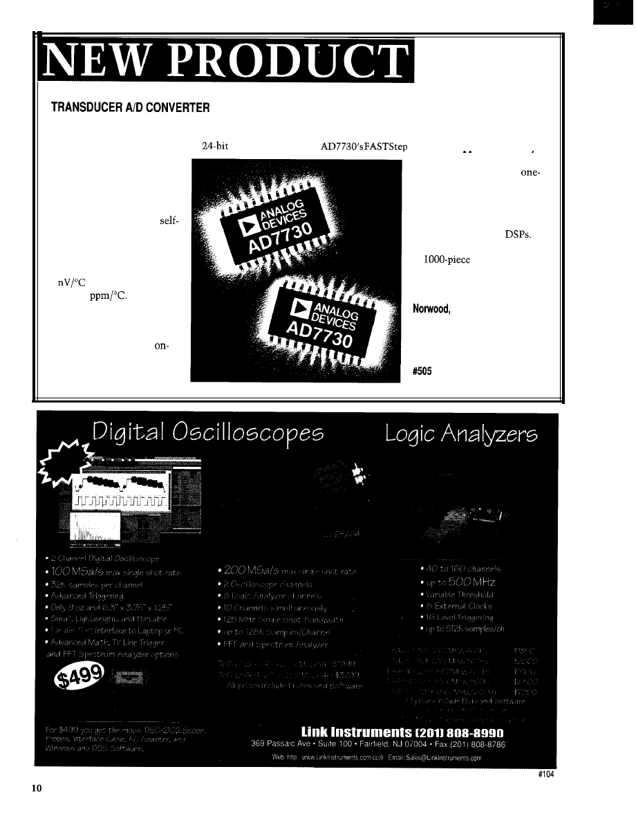
NEWS
The AD7730 is a high-resolution analog front end for
for synchronizing AC excitation of the bridge are also
weigh-scale and pressure measurement applications.
provided. If large weight changes occur on the load cell,
Operating from a +5-V supply, this
sigma-delta
the
mode closely approximates (by
ADC accepts low-level ana-
log signals from a transducer
and outputs digital words.
The AD7730 provides a
resolution of 220,000 counts,
peak-to-peak. It contains
and system-calibration op-
tions and provides a unique
chopping scheme that results
in a typical offset drift of
5
and a maximum gain
drift of 2
Featuring
two buffered differential
programmable-gain analog
inputs, the chip accepts eight
analog input ranges. An
chip, 6-bit DAC for removing
tare voltages and clock signals
switching between internal
filters) the final result in
eighth of the final output set-
tling time. Its serial port can be
configured for three-wire op-
eration and is compatible with
microcontrollers and
The AD7730 sells for $9.86
in
quantities.
Analog Devices, Inc.
One Technology Way
MA 02062-9106
(617) 937-1428
Fax: (617) 821-4273
www.analog.com
Issue
87 October 1997
Circuit Cellar INK@
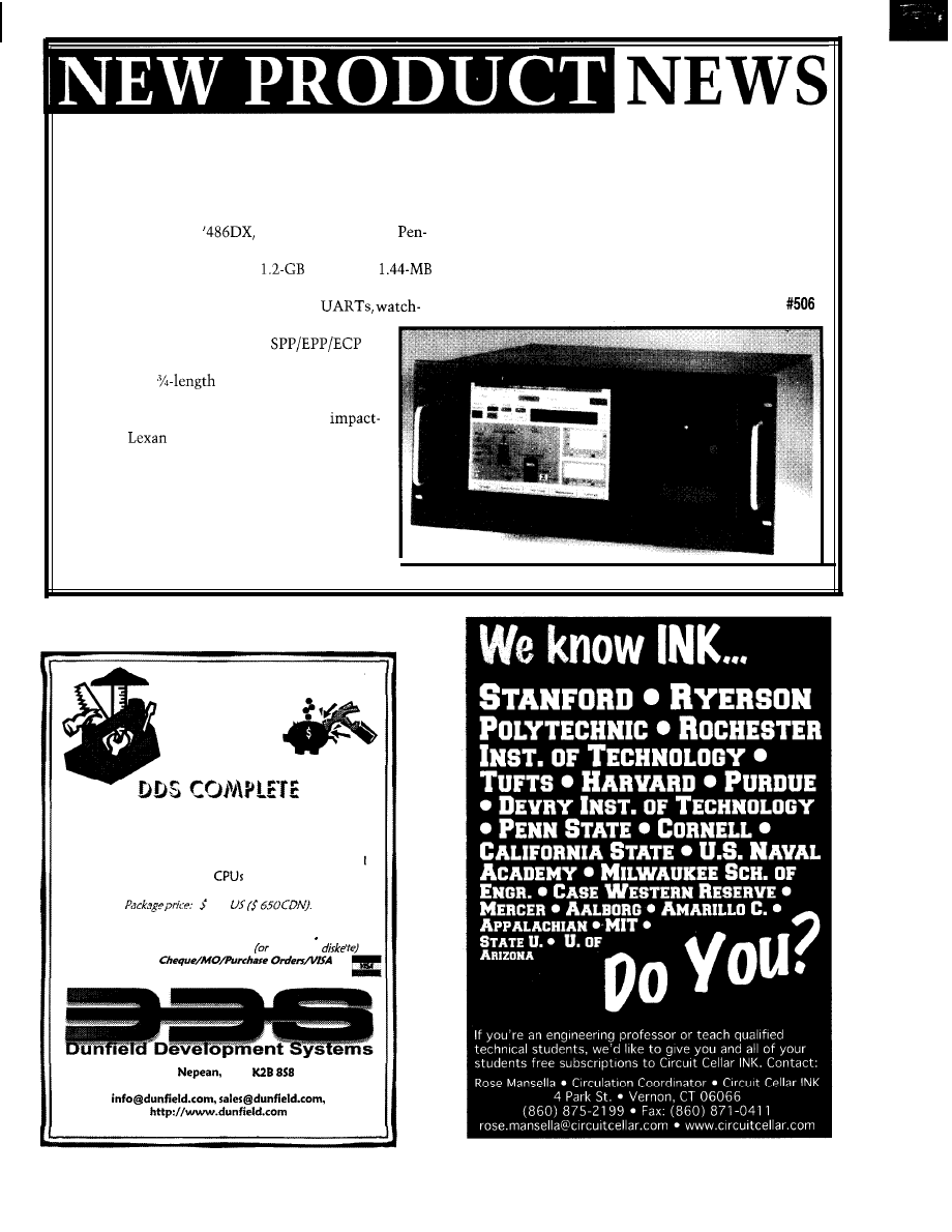
INDUSTRIAL COMPUTER
The IND-600 is a PC that combines a 10.4” TFT or
industry-standard development tools and industrial or
STN color display with a plug-in industrial CPU board in
scientific application software packages.
a rugged rack/panel-mount enclosure. It can be equipped
IND-600 pricing starts at $2788.
with a cost-effective
a midrange ‘586, or a
tium microprocessor for maximum performance.
lndocomp Systems, Inc.
Standard features include a
hard drive,
5409 Perry Dr.
l
Waterford, MI 48329
floppy drive, and 4-MB DRAM (expandable to 128 MB).
(248) 673-7315
l
Fax: (248) 673-8370
It also has two serial ports with 16550
www.indocomp.com
dog timer, keyboard interface, and a high-perfor-
mance parallel port supporting
modes. A field-replaceable 250-W power supply is
built in. Four
ISA-bus slots provide
room to install network and data-acquisition
boards. The front panel is fitted with an
resistant
window to ensure reliable opera-
tion-even in harsh environments. Shock-mounted
disk drives and adjustable board-hold-down brack-
ets eliminate the effects of shock and vibration.
MS-DOS is preloaded on the hard drive, and
Windows is available as a factory-installed op-
tion. This combination provides easy access to all
Looking to fill your embedded
toolbox without
breaking the
bank???
Everything you need, all in one convenient package!
Includes all of our Micro-C Compilers, Assemblers,
Simulators, Disassemblers, Monitors, Project Plans, and
Data Line Monitor. Many
supported, including
C-FLEA, a virtual CPU you can use anywhere.
XX?
Call or write for our free catalogue
FREE Demos available on BBS or WEB
rend $5 for
We
accept
P.O. Box 31044
Ont.
CANADA
Tel: 613-256-5820 Fax: 256-5821 BBS: 256-6289
Circuit Cellar INK@
Issue
87
October 1997
11
FEATURES
Analog Data Acquisition
DTMF Message Decoders
Interprocess Communication
Compressed-Code
Analog Data Acquisition
Damon Chu
any systems now
demand data-acqui-
sition functionality. A
microcontroller-based
design enables the measurement, pro-
cessing, control, and communication
functions required by these applica-
tions, while keeping system costs low.
In this article, I discuss how a new
microcontroller can create the founda-
tion of a sophisticated data-acquisition
system. Taking a home-security sys-
tem as an example, I demonstrate how
to use the
feature set for maxi-
mum functionality.
But, let’s start with a brief overview
of this new 8-pin, 8-bit MCU.
ITS BITS AND BYTES
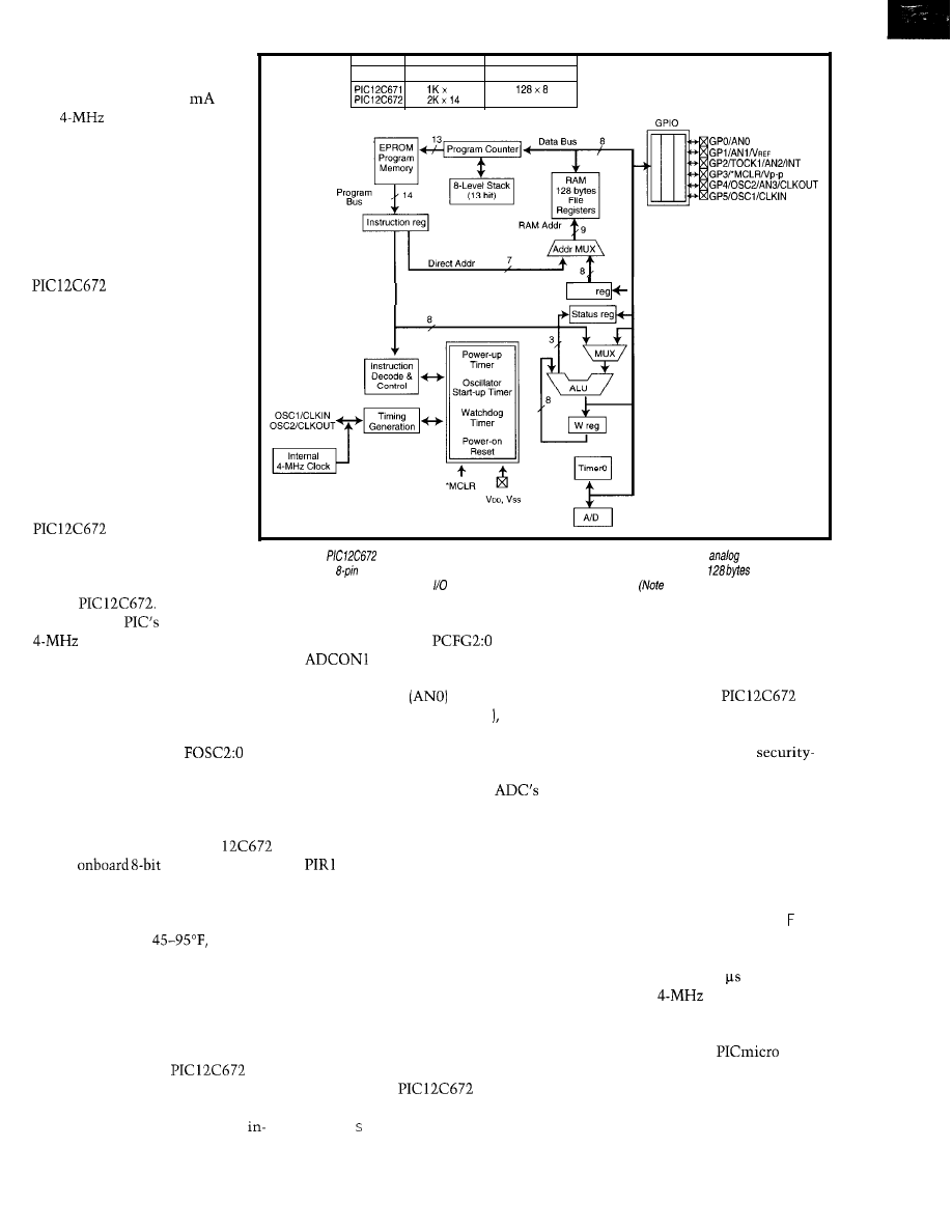
Depicted in Figure 1, the
features 2048 words of program mem-
ory along with 128 bytes of user RAM.
Advanced analog features include an
on-chip ADC and four analog chan-
nels, which can be used for measuring
environmental conditions (e.g., tem-
perature, pressure, motion, and voltage).
The device offers five multiplexed
I/O pins (plus one input only) with
chip clock oscillator (4 MHz), 35
word instructions, full-speed 1-ys
instruction cycle at 4 MHz, and an
eight-level-deep hardware stack.
It also includes an 8-bit clock/
counter with 8-bit programmable
12
Issue
87
October 1997
Circuit Cellar INK@
scaler, watchdog timer, direct
LED drive, low 2.5-5.5-V operat-
ing voltage, and under 2
at
5-V,
low-power consump-
tion. In-circuit serial program-
ming of the OTP controller offers
a true, self-contained intelligent
system on chip (see Photo 1).
Devices
Program Memory Data Memory (RAM)
14
1 2 8 x 6
Despite its small packaging,
it offers high-performance RISC
functionality.
This combination makes the
particularly appro-
priate for many data-acquisi-
tion applications in which the
environment is being moni-
tored and/or measured in a
variety of products. The MCU
can also provide a high-perfor-
mance, low-cost replacement of
many electromechanical appli-
cations.
FSR
DESIGNING IT IN
Let’s
look at how the
can be used in a
home-security system. Since
my system is AC powered, its
power supply provides the 5 V
for the
Figure 1 --The
provides advanced analog features, including an on-chip
ADC
and four
channels. The
newest family of
B-bit microcontrollers
offers 1024-2048 words of program memory along with
of user RAM.
These
devices feature six multiplexed pins with on-chip clock oscillator (4 MHz).
that higher order bits are from the
STATUS register.)
I chose the
internal
clock oscillator as the system
clock. Its use not only eliminates the
space and cost of an external clock
oscillator but also frees pins 2 and 3 to
be general-purpose I/O pins.
The internal clock oscillator is
selected by setting bits
in the
configuration word to a binary value of
100. The configuration word can be set
up during the in-circuit serial-program-
ming process.
puts by setting bits
in the
register to the binary value
of 100, establishing pin 7 as analog
input channel 0
and pin 6 as
analog input channel 1 (AN1 so now,
analog measurements can be taken.
ing the A/D conversion. The microcon-
troller wakes up once the conversion is
complete and the A/D interrupt occurs.
Configuring the ADCONO register
to the hex value of Cl opens channel 0
for measurement, selects the
own clock, and turns on the converter.
Interrupts are enabled by setting the
appropriate bits in the INTCON and
registers.
For processing, the
is a
well-equipped engine. With 2048 x 14
words of program memory storage and
128 bytes of user RAM, the
systems designer has sufficient memory
resources to implement averaging
routines.
For measurement, the PIC
has an
ADC. A resolution
of 256 steps is sufficient for most sen-
sor needs in a home system, especially
given that the typical home thermo-
stat has a range of
requiring
measurement of 50 steps at a resolu-
tion of 1°F. With the ability to config-
ure four channels of analog input, the
ADC can measure four sensors while
the processor is in the power-down
sleep mode.
Analog conversion is started by
setting the GO bit in ADCONO. Once
a conversion completes, an interrupt
signal is generated, and the device
begins processing the input measure-
ment. Listing 1 shows code for an A/D
conversion.
All system RAM locations reside in
the register file and are available for
every CPU cycle, so all registers are
available for data manipulation on
every cycle.
APPLICATION TUNING
For sensor readings, the ADDW and
RR F instructions can perform addition
and division by powers of 2. Each in-
struction executes in 1 when using
the internal
system clock oscil-
lator. Its eight-level-deep hardware
stack supports a number of nested loops.
In my system, the
mea-
sures temperature and carbon-mon-
oxide concentration. Two of the six
I/O pins are configured as analog
For power-conscious systems, the
A/D conversion can take place while
the rest of the
is asleep. To
make this change to the code, simply
add the 1 eep instruction after start-
If you’re using the
archi-
tecture, it’s a good idea to set aside a
section of program memory to store
look-up table values. These table values
can be accessed via CA L L and RET LW
Circuit Cellar INK@
Issue 87 October 1997
13
instructions by sending the program
counter into the table at a specified
location and returning with the look-up
value. Thus, the processed result can
be matched to the look-up table value.
For example, that match might mean
a certain toxic-gas ppm level is reached
and action must be taken. Or, in the
case of measuring IR radiation, after
comparing the measured and processed
data to the table look-up value, the
heat level could determine whether
human intruders are in the house or if
it’s just the cat arriving home.
After the chip has executed the
processing algorithms and made its
comparison to table look-up values,
action may be required. Control may
be as simple as turning on the air con-
ditioner if the temperature is above the
nominal setting or switching on a
bright light if intruders are detected.
The
multiplexed pins
can be configured through software to
provide up to six digital lines-five
bidirectional and one input only. Here,
pins 6 and 7 are being used for analog
measurements, and pins 2-S are avail-
able for general-purpose DIO functions.
As the six pins are highly multiplexed,
the GPIO register must be set up prop-
erly to establish whether the pins
provide I/O or non-I/O functions.
Once the pins’ functionality is cho-
sen, the bidirectional I/O pins must
have their direction defined via the
TRIS register. A logic 1 from the TRIS
register bit puts the corresponding
output driver into high-impedance
mode, allowing it to be a digital input.
Conversely, a logic 0 puts the contents
of the port’s output latch on the se-
lected pins, enabling the output buffer.
For outputs that are enabled, each
of the output drivers provides 25
of drive current. That level is suffi-
cient for turning on/off power transis-
tors or
and for lighting bright
This function can provide system
recovery in the event of a software
malfunction, and it can run during
Sleep mode. It’s set up during the
programming process by setting WDTE
(watchdog timer enable bit) in the
configuration word.
In addition, pin 2 can be configured
as a clock input (TOCKI), enabling
synchronization with an external sys-
tem clock using TMRO. TMRO is a
16-bit overflow counter with an 8-bit
programmable prescaler. An overflow
of TMRO can interrupt the processor
during operation.
Finally, the
can be reset
via an external RESET signal or by
various timeouts built into the micro-
controller. Of course, how you use
these features depends on the com-
plexity of your system.
For communication, the
incorporates the capabilities of other
families. For a stand-alone
security system,
are often suffi-
cient in communicating status.
Each pin configured as an output
can provide 25
of drive current. In
a more complex system (e.g., commu-
nicating RS-232 to a PC’s serial port),
the fast instruction-execution rate of
ables the
to bit bang the
RS-232 protocol.
The information can then be trans-
mitted to a PC running the Windows
Terminal program. Four pins are re-
quired-one for TOCKI, two outputs,
and one input.
For transmit mode, TIMER0 gener-
ates the timing to send each bit of the
serial stream. The value of the TIMER0
prescaler is determined by the input
clock frequency and the data rate. The
transmit pin (TX) can be any of the I/O
pins set up as an output.
For receive mode, the receive pin
(RX) must be connected to TOCKI to
detect the asynchronous start bit of
any transmission. The Option register
is set up so TIMER0 is in counter mode
and set to increment on the falling edge.
The chip’s computational power
supports parity generation. On recep-
tion of a packet, parity can be computed
on the received byte and compared to
the ninth bit received. Depending on
system requirements, other protocols
can be implemented (e.g.,
or designer proprietary interface).
From the input standpoint, the
is equipped with interrupt
on pin change. This capability lets
push buttons, for example, be designed
into a system, enabling direct control
of the microcontroller. By pressing a
button, the CPU is interrupted and goes
off into a subroutine [e.g., checking the
CO level) at that precise moment.
Its
architecture saves space,
and its integration reduces component
count. The on-chip
system
clock oscillator eliminates the need for
an external oscillator. Its ability to
store sensor calibration information in
table look-up form in program memory
space obviates the need for off-chip
memory storage.
In some systems, pull-up resistors
are used when connecting to
collector transistors and similar cir-
cuits. The
under software
control can select internal pull-up
resistors at the I/O pins. In some manu-
facturing environments, the ability to
uniquely program the contents of pro-
gram memory for a number of systems
is required.
Many sensor applications require a
calibration step to measure and store
offsets, slopes, and configuration
Listing 1 --Programming
code is used to configure four channels of analog input (four sensors) for the
conversion process.
BSF
STATUS, RPO
select page 1
CLRF
configure A/D inputs
enable A/D interrupts
BCF
STATUS, RPO
select page 0
MOVLW
select RC clock, A/D on, Channel 0
MOVWF ADCONO
BCF
clear A/D interrupt flag bit
BSF
INTCON, PEIE
enable peripheral interrupts
BSF
INTCON, GIE
enable all interrupts
Add sampling delay routine to ensure that required sampling
time for selected input channel has elapsed. Conversion may be
started after this delay.
ADCONO, GO
start A/D conversion
14
Issue
87 October 1997
Circuit Cellar
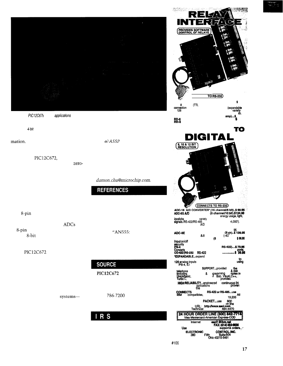
Photo l--The
targets
in which the environment
(i.e., pressure, temperature, motion,
acceleration, gas concentration, and sound) is being monitored and/or measured in a variety of products. The B-pin
microcontrollers enable easy integration of first-time intelligent features into electromechanical designs and compete
directly with
microcontroller products while providing enhanced performance.
Potentiometers or discrete
serial EEPROM devices can set up and
store this calibration information.
With the
the in-circuit
serial programmer provides for a
component-count method. Using five
pins, each sensor module can be pro-
grammed with a unique set of calibra-
tion parameters to bring any sensor
tolerances to within the required accu-
racy.
And last but not least, the combina-
tion of an ADC with a PICmicro engine
in an
package provides the most
effective space and component savings.
There aren’t many discrete
in
an
package-let alone an ADC
with an
RISC MCU.
IT’S A SMALL WORLD?
The
provides in a small
form factor all the capabilities needed
to measure and process sensor informa-
tion as well as the control and commu-
nication driven by that information.
Everyday products such as battery
chargers, rice cookers, toasters, ther-
mometers, rheostats, thermostats,
security systems, sensors
anything that measures the surround-
ing environment-now can have all
the capabilities found in larger, com-
plex systems.
q
Damon Chu is strategic marketing
manager for the Standard Microcon-
troller
Division at Microchip
Technology. He has spent more than
15 years in chip design, DSP, and micro-
controller systems with companies
such as Microchip, Analog Devices,
VLSI Technology, and RCA Advanced
Technology Labs. You may reach him
at
J. Day, “AN656: In-Circuit Serial
Programming of Calibration Pa-
rameters Using a PICmicro Micro-
controller,” Embedded Control
Handbook, 1, Microchip Technol-
ogy, Chandler, AZ, 1997.
S. Fink,
Software Imple-
mentation of Asynchronous Serial
I/O,” Embedded Control Hand-
book, 1, Microchip Technology,
Chander, AZ, 1997.
Microchip Technology, Inc.
2355 W. Chandler Blvd.
Chandler, AZ 85224-6199
(602)
Fax: (602) 786-7277
www.microchip.com
401 Very Useful
402 Moderately Useful
403 Not Useful
(C
ONNE
CTS
AR-16 RELAY INTERFACE (16 channel) . . . . . . . . . . . . 69.66
Two channel
level) outputs are provided for
to relay cards or other devices
to
relays using EX-16 expansion cards). A
of
relays cards and relays are stocked. Call for more in
AR-2 RELAY INTERFACE (2 relays, 10
44.63
REED RELAY CARD (9 relays, 10 VA) . . . . . . 49.95
RELAY CARD (10 amp SPDT, 277 VAC)...S 69.9%
A N A L O G
CONVERTER*
Input voltage. amperage. pressure,
and a wide
of other types of analog
available (lengths to
Call for info on other
configurations and 12 bit
converters (terminal block and cable sold separately).
Includes Data Acquisition software for Windows
or 3.1
TEMPERATURE INTERFACE’
Includes term. block temp. sensors
lo 146’ F).
STA-9 DIGITAL INTERFACE*
channel) . . . . . . . . .
status of relays, switches, HVAC equipment,
devices, keypads, and other devices.
PORT SELECTOR (4 channels
an RS-232 port
into 4 selectable RS-422
to
converter) . .
your interface to control and
monitor up to 512 relays, up to 576 digital inputs, Up
the
or up to 129 temperature inputs
X-16, ST-32 8 AD-16 expansion cards.
l
FULL
TECHNICAL
over
by our staff. Technical reference
test software pro
exam
GW Basic, Visoa
Assembly and others are
l
for
hour industrial a
performance in
with 10 years of
energy management field.
.
TO RS-232,
with
and
Mac and most computers.
standard baud rates and protocols (50 to
baud).
FREE INFORMATION
our
number.
Fax or E-mail to order, or visit our Internet
Catalog.
Support (614)
E-mail:
International 8 Domestic
for information, technical
ENERGY
South
Street,
Columbus.
Circuit Cellar INK@
Issue
87
October 1997
DTMF
Message
Decoders
Steven Kraft
Telephone Aids for
the Hearing Impaired
pacedadvancement
in communications
technology with its
speed data fax and E-mail, we often
take for granted the more personal
experience afforded by simple voice
communication on the telephone.
It’s common for many of us to as-
sume the party at the other end is
equally equipped with the latest hard-
ware, software, and technical knowl-
edge. Unfortunately, not all are active
participants in these advancements.
Many hearing-impaired individuals
also are unable or unwilling to embrace
these modern means of communication.
Perhaps their hesitation is due to the
cost of the hardware, or maybe they’re
unable to master using a computer
keyboard.
Grandma’s hearing may be getting
worse as each year passes, but she
doesn’t need to miss out on your calls
just because she cannot make out
many of your spoken words over the
phone. In many cases, all she needs is
a simple communication aid to get
across those words or phrases she can’t
seem to hear right.
A DTMF message decoder is just
the ticket to improve the accuracy of
voice communication. It restores the
enjoyment of what has become a diffi-
cult communication experience.
This DTMF message-decoder project
is based on the Motorola
microcontroller and a
x
character LCD readout. Although
conceived independently for this appli-
cation, it is quite similar to the HCS
Message Man project that appeared in
Jeff Bachiochi’s “Talking on the Phone
Without a Word”
40).
It differs in two important respects.
It has a more intuitive alphanumeric
keypad decoding scheme. And, software
hooks enable you to use an optional
IBM PC parallel port interface to speed
up alpha key entry.
A USEFUL INEXPENSIVE SOLUTION
The most common method of tele-
phone communication with
impaired persons essentially consists
of a TTY or teletype device connection
at each end of the phone line. It’s pos-
sible to combine both voice and TTY
communication on the same call, but
the necessary procedure is somewhat
inconvenient.
If your phone isn’t equipped with
this hardware, you must use a special
relay service where a relay agent trans-
lates your words onto the TTY, com-
promising your conversation’s privacy.
You also have to consider the cost of
this special hardware for both parties.
Modem communication is the only
other option. Unfortunately, commonly
available hardware precludes its use
when voice communication is predomi-
nant during the call. Otherwise, you
need either two dedicated lines for
separate voice and data or the latest
DSVD (digital simultaneous voice and
data) modem.
These new modems allow you to
multiplex both voice and data on a
single phone line. However, you again
have the cost of computer and modem
hardware for both parties. And when
you don’t have your modem with you,
the only way to communicate via tele-
phone is by voice.
By instead relying on the universal
DTMF encoding standard, it’s possible
to transmit words or short messages
(albeit much more slowly) using any
telephone anywhere with a standard
touch-tone keypad.
You don’t need any special hardware
on the transmitting end and only the
18
Issue 87
October 1997
Circuit Cellar INK@
easily operated inexpensive
DTMF message decoder on
DTMF Primary
Repeat
Repeat
Num Lock
Key
Key once
Key twice
Mode On
the receiving end. This ar-
Name (1st Alpha) (2nd Alpha)
(3rd Alpha) (Numeric)
rangement conveniently
allows the combination of
1
Q
Z
1
2
C
2
both voice and
3
E
F
3
coded messages on the same
4
H
4
phone line.
5
J
K
L
5
6
M
N
0
6
7
P
7
CIRCUIT DESCRIPTION
8
T
U
V
8
The complete circuit sche-
9
W
X
9
0
backspace
backspace
0
matic diagram for the DTMF
l
clear display
clear display
message decoder is shown in
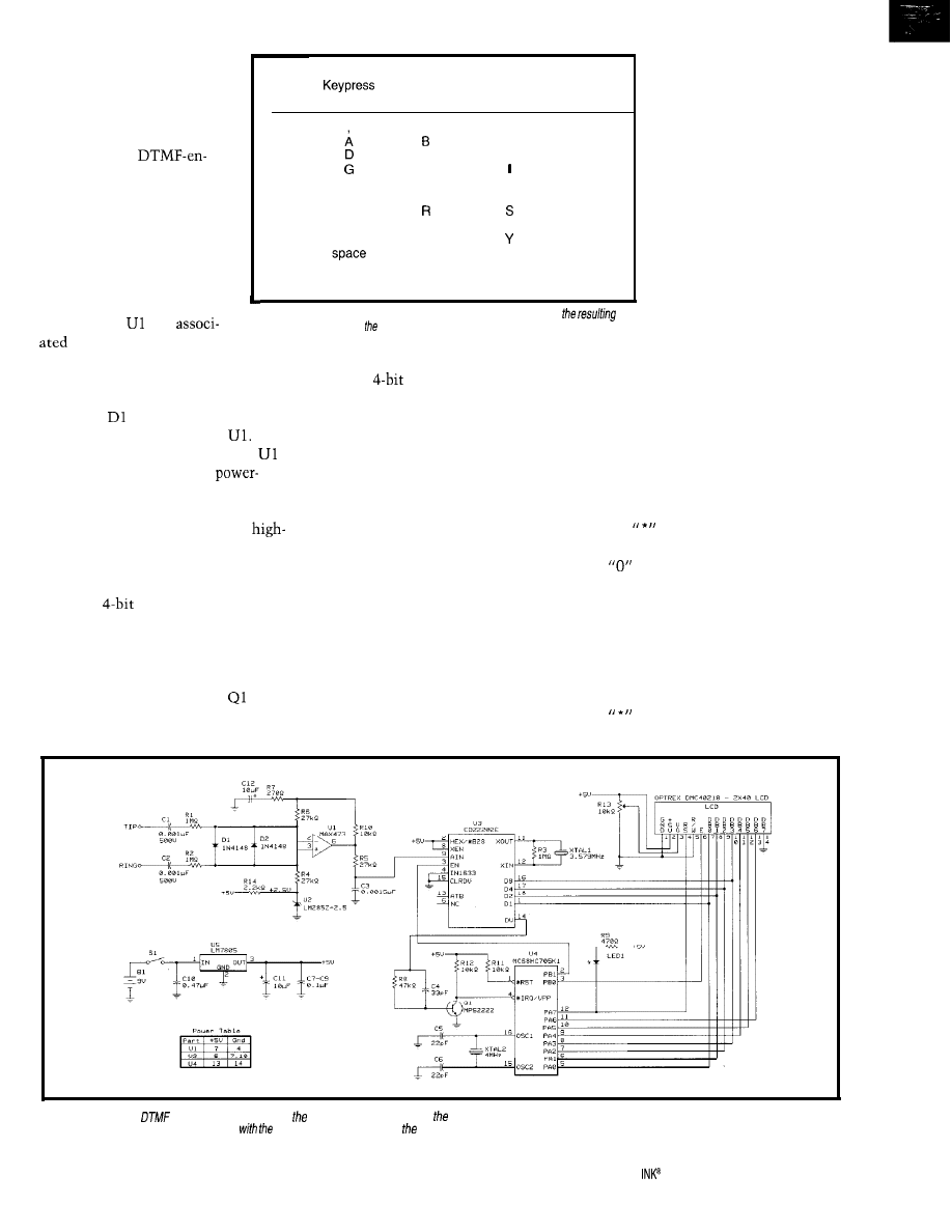
#
num lock
Figure 1. The op-amp circuit
consisting of
and
Table l--This
fable shows the correlation between key presses and
characters displayed oh
LCD.
A “repeat key” is pressed again within 0.7 s of ifs
resistors and capacitors
first pressing.
is a unity-gain audio-signal amplifier
that provides a high-impedance inter-
face with the phone line.
Diodes
and D2 serve as ringer
voltage clamp protection for
The
2.5-V reference U2 is used to bias
halfway between the O-5-V
supply rails to achieve maximum out-
put signal swing. A low-pass filter
formed by R5 and C3 attenuates
frequency noise.
an interrupt condition, it immediately
reads the
DTMF data from U3 and
then converts it to the appropriate code
for controlling the LCD module. R13
controls LCD contrast, and LED1 serves
as a flashing power-on indicator.
Power for this circuit is supplied by
a 9-V battery regulated down to 5 V by
voltage regulator U5.
(e.g., A is sent with a single
press of the 2 key).
If your letter is the sec-
ond one assigned to that key,
you must press the key
twice within a 0.5-s time
period. B is sent with two
rapid presses of the 2 key.
If you wait too long (i.e.,
more than 0.7 s) between
presses, the decoder inter-
prets the second press as the
next letter of your message.
You’d have sent the two
letters “AA” instead of the
single letter “B”.
On the other hand, if you want to
send two consecutive letters, both
assigned to the same key, you should
wait at least one full second after press-
ing this key for the first letter before
pressing it again.
In addition to sending letters A-Z,
you can also send a comma by pressing
U3 is an integrated DTMF decoder
IC that converts standard touch tones
into their
binary-encoded equiva-
lent representation. When a valid DTMF
signal is detected, this code is latched
into the output port of U3 and the Data
Valid signal at pin 14 becomes active.
This signal is inverted by
which
drives the external interrupt pin of
microcontroller U4. When U4 detects
OPERATION
Any standard touch-tone phone may
be used to send brief messages (up to
two lines of 40 characters) to the mes-
sage-decoder unit connected at the
other end of the line. Allowed charac-
ters include all capital letters of the
alphabet, the numbers O-9, commas,
periods, and spaces.
To send the first letter of your mes-
sage, just press the desired key once
the
“1”
key once or a period by press-
ing the key once. To put a space
between words in
your
message, press
the
key once.
To correct the previous character,
backspace one character position by
pressing the “0” key twice in rapid
succession.
If you need to start your message
from the beginning or to erase a previ-
ous message from the display, press
the key twice rapidly. This action
clears the display and enables you to
Figure l--Received
signals are processed and resulting characters sent fo LCD module configured for B-bit data-transfer mode. A blinking LED “system active”
indicator time shares processor output PA7
data/command select pin of LCD.
Circuit Cellar
Issue 97 October 1997
19
“Total
by
Operate TV, lamps and other
appliances from up to 100 feet
away. Turn-on house lights
from your car. Simple to hook-
up
and use. Includes two
receivers on separate fre-
quencies and a two button
hand-held transmitter that
controls them. Requires
9 volt battery (not included).
Clam-shell display packaging.
CAT # TCR-1
PAINFULLY BRIGHT RED LED
2500 to 4000 mcd 20 ma. These
T 1 314 (5 mm diameter) red
are
significantly brighter than conventional
At close range, they are painful
to look at. They are great for attention getting
displays that can be seen from a distance.
10 for $5.00
l
100 for $45.00
1000 for $400.00
MC341
power audio amplifier suitable
speakerphones or talking picture
frames. The 8 pin DIP package
requires only a few additional parts, operates
on 2
16
volts and drives speakers of 8 ohms
or greater. Output power exceeds 250
with 32 ohm speaker. Power-down option
saves power in battery driven applications.
Hook-up sheet. Large quantity available.
6 0
CAT MC341
Pieces $25.00
TERMS. NO MINIMUM
ORDER
and
the
A
$5.00
per order All others
AK,
PR or Canada
pay full
shipping.
All orders
CALIFORNIA must
state
tax.
CALL.
WRITE
NO COO. Prices subject
or E-MAIL
our
96 Page
CATALOG
K
Display Character
Figure
interrupt service
routine
uses a 0.7-s timeout function to control program
flow. determines which character to display based
on the
of the keypad
1
start
from the first character position
To send a number, first press the
of the first line.
key once. This action puts you in
Messages longer than 40 character
the numeric mode, and all keys are
positions automatically wrap to the
interpreted by the decoder just the way
second line of the display. If your
the numbers appear on the key pad.
sage exceeds 80 characters total, you
In numeric mode, you also can send
begin overwriting the first line of your
a decimal point (period) character. To
message. So, be sure to clear the
return to the letter mode, just press
ous message before starting a new one.
the
key again.
20
Issue
87 October 1997
Circuit Cellar
INK@
Listing l--This simple
program is used enter messages via PC keyboard
single-line
character input.
up to characters to be entered, edited, and automatically
encoded
1
4
5
6
7
8
9
10
12
14
16
18
20
22
24
26
28
30
32
34
36
38
40
42
44
46
50
51
52
53
54
55
56
57
58
62
64
66
70
72
74
76
REM ****** DTMF MESSAGE ENCODER PROGRAM ************
CLS DIM
DIM
=
DATA 124,124, 12, 60,127, 15, 79,143, 31, 95,159,
DATA
76, 77,
28, 29, 30, 92, 93, 94,156
DATA
157,158, 44, 13, 45,
14
FOR I = 0 TO 39: READ LOOKUP%(I): NEXT
port =
REM Address of parallel port used.
LOCATE 10, 25: PRINT "DTMF MESSAGE ENCODER PROGRAM"
LOCATE 15. 25: PRINT "COPYRIGHT
1995 ELECTROKRAFT"
REM
REM Determine
DELAYCOUNT value for host computer.
TIMER ON
ON
900
FOR = 1 TO 10000000: NEXT
LOCATE 20, 30: PRINT PRESS ANY KEY
I”
DO WHILE
=
LOOP
REM
REM Input up to
message string and encode as
CLS
= 61: REM Clear LCD before message.
FOR I = 1 TO 40: PRINT
NEXT
FOR I = 1 TO 40: PRINT
NEXT
LINE INPUT
=
IF =
THEN END
FOR I = 1 TO
=
I.
NEXT I
REM
REM Output DTMF data codes to parallel port.
FOR I = 0 TO
OUT port,
OUT port 2,
FOR = 1 TO DELAYCOUNT&: NEXT
REM
TONE ON.
OUT port + 2, &HO
FOR = 1 TO DELAYCOUNT&: NEXT
REM
TONE OFF.
OUT port,
16
OUT port + 2,
FOR = 1 TO DELAYCOUNT&: NEXT
REM
TONE ON.
OUT port + 2, &HO
FOR = 1 TO DELAYCOUNT&: NEXT
REM
TONE OFF.
IF I = 0 THEN 70
=
I,
IF
= 0 THEN PRINT ELSE PRINT
NEXT I
PRINT BEEP: REM DTMF Message Transmission Completed.
GOT0 32: REM Ready for next message.
REM
900 REM ON 6-s timeout EVENT Calculate
DELAYCOUNT value.
901 TIMER OFF
902 DELAYCOUNT& =
100 + 1
903
= 9999999
999 RETURN
PROGRAM DESCRIPTION
Performing these functions requires
the internal
PROM to be
programmed with the DTMF
decoder firmware.
The program begins by initializing
I/O ports A and B and defining all bits
as outputs. All variables are cleared
after enabling both real-time interrupt
and external interrupt functions.
An internal timer is programmed to
generate real-time interrupts every
65 ms. The program uses these prima-
rily for the
repeat key timeout
function.
After a l-s power-up delay, the LCD
module is initialized by sending a
sequence of four 8-bit control codes to
the module via port A. Following the
output of each
code, a display
subroutine waits 600
(to
accommo-
date the LCD processing delay] and
then strobes the LCD enable line via
port bit PBO.
PC Development Took
No M
ORE
C
RASH
B
URN
EPROM
Technology
DOS Single Board Computer
572
FLASH
Memory
drive
10
Mhz CPU 2 Timers
512 k bytes RAM
4 Interrupt
512 k/256 k FLASH 8 Analog Inputs
2 Serial Ports
X-Modem File
24 Parallel Lines
Transfer
INCLUDES DOS Utilities
8 Channels, 12 Bits
6 Conversion Time
Clock/Calendar Option
Includes Drivers
8 Opto-Isolated Input:
Cost Effective
JK micros stems
Control for
TO ORDER (510) 236-1151
FAX
our
WEB
1275 Yuba Ave., San Pablo, 94806
Circuit Cellar
INK@
21
This same subroutine gets called
each time a character is output to the
LCD module. Port bit PA7 is set to
logic zero for control data or logic one
for character data.
After displaying a start-up message
for 3 s, the LCD is cleared and the pro-
gram enters a perpetual wait loop where
it flashes the LED power-on indicator.
It is ready to receive and decode DTMF
messages sent over the phone line.
The IRQ input to U4 is pulled low
each time U3 detects a valid DTMF
signal. This external interrupt causes
the program to temporarily suspend
execution of the wait loop while servic-
ing the interrupt.
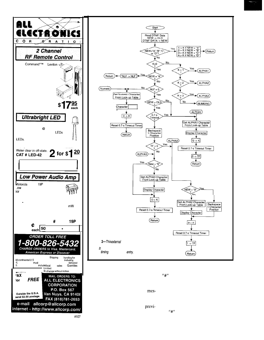
Figure 2 shows the program flow for
the external interrupt service routine. It
starts by calling a subroutine to read the
DTMF data from the output port of U3.
This subroutine first redefines port-A
bits O-3 as inputs to the microcontroller
and then enables the U3 output port.
DTMF data is now read into one of the
internal RAM locations of U4. Port-A
bits O-3 are then set to function again
as outputs.
Variable is used for processing the
auxiliary DTMF codes (separate keys
labeled A, B, C, and D which do not
appear on most standard
phones).
These auxiliary codes can be used by
the program in conjunction with an
optional IBM PC interface.
Bit flag NLF controls a num 1 ock
mode via the
key. Timeout flag T F
controls the program flow when keys
are repeatedly pressed within the 0.7-s
timeout period. Table 1 shows the
correlation between key presses and
the resulting displayed characters.
SPEED IT
LITTLE
Some patience and practice is re-
quired to master effective communica-
tion from a touch-tone keypad. The
slow rate of character entry limits real-
time communication to at most a few
words or short phrases per exchange.
If you happen to have a portable IBM
PC handy, you can transmit messages
to the same DTMF message decoder
much more conveniently by using an
optional IBM PC interface. Figure 3
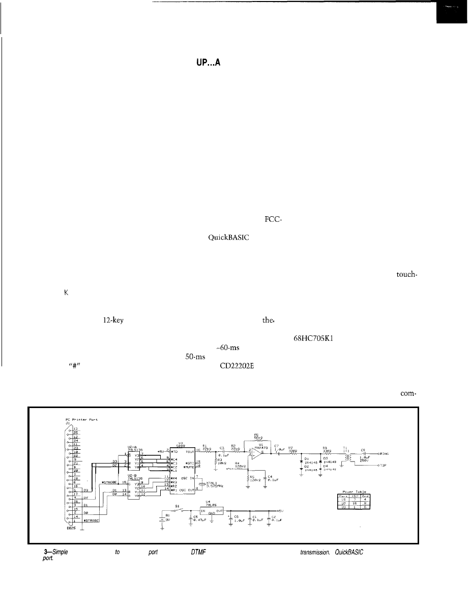
shows the circuit used between paral-
lel printer port and telephone line.
This telephone-line connection
circuitry is intended for experimental
use. Any commercial application
would require substitution of an
registered DAA module.
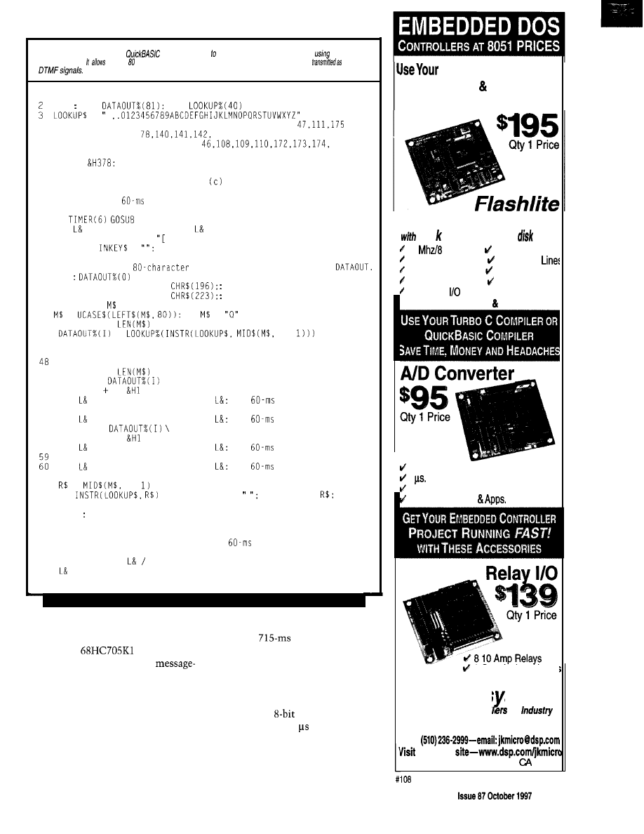
A complete
listing for
this PC printer port interface is shown
in Listing 1.
The PC keyboard is used to enter
single-line messages up to 80 characters
long-displayed on the PC monitor.
Pressing Enter sends these characters
(encoded as a sequence of two DTMF
codes per character) to the DTMF mes-
sage decoder at the other end of
telephone line.
A crude but effective software delay
loop generates an
delay to sat-
isfy the
minimum tone-duration
requirement of the
receiver/
decoder chip.
This DTMF message-encoder inter-
face is much more convenient to use
and achieves a relatively blazing trans-
mission rate of four characters per
second. Still, it’s faster than manual
entry on a touch-tone keypad.
BOXING IT UP
Almost any packaging scheme can
be used for the DTMF message decoder.
Since the LCD module dimensions are
long and narrow, unlike readily avail-
able project boxes, I opted for a simple
custom enclosure.
The 2” x 6” decoder circuit board
and LCD module were mounted in a
2.5” x 2.5” x 10” metal enclosure formed
by bending two precut pieces of 10” x 4”
aluminum. A pair of triangular wooden
endpieces complete the enclosure.
Install a fresh 9-V battery and turn
on the power. You should see a start-
up message displayed for -3 s, after
which the display clears and the LED
begins flashing at a l-Hz rate.
R13 controls display contrast for
optimum viewing in ambient room
light. To test the unit, connect it to any
phone jack having an accessible
tone phone connected to the same line.
ON THE PHONE AGAIN
In all honesty, this project was as
much an excuse to learn how to use an
inexpensive microcontroller like the
as it was an opportunity
to create something personally useful.
Grandmother’s hearing loss was
serious enough to warrant some simple
communication aid beyond an ampli-
fied telephone. I wanted a solution
that partially preserved the voice
Figure
hardware connected a PC printer
uses the 5089
tone-generator chip to speed up message
A
program
controls fhe
printer
22
Issue
87 October 1997
Circuit Cellar INK@
Megatel Offers a W i d e Range of Embedded PC Architecture
‘Embedded
for the
On-Board Features such as:
l
8088 or
Processors
l
Local Bus Super VGA supporting LCD Panels
l
Up to
DRAM
l
Ethernet Local Area Network
l
On-board programmable
l
Low Power Consumption
l
Operation
volts only (typical)
l
2 IBM compatible RS-232C Serial Ports
l
general purpose Parallel
Port
l
Only 4” 4” form factor
l
ISA or PC1104 Bus compatible options
f a x :
Incredibly powerful
At 50 instruction
time,
our
delivers
the power that an
8
or
controller can’t.
Inherently
We’ve
included everything to handle even the
most demanding industrial
requirements.
simple
Easy to
program, run, and get
going!
Fax: 303-690-1875
Web
24
Issue
87 October
1997
Circuit Cellar INK@
munication experience and yet was
inexpensive, convenient, and easy to
use from any location.
The DTMF messaging approach may
seem unbearably slow-until you’re
communicating with a person who
only understands 50% of your spoken
words. Then, this turns out to be a
wonderfully useful aid.
q
Steven Kraft is an electrical engineer
and holds an MSEE from the Univer-
sity of Colorado.
He has
worked on
satellite control electronics and is
currently a part-time consultant in-
volved with electronic security-system
sensor design. You may reach him at
The complete listing of
. ASM
is
available on the Circuit Cellar
Web site.
DTM
19
contains the
object code.
DMC40218
LCD
module),
MAX473
op-amp
Corp.
701 Brooks Ave. S
Thief Falls, MN 56701-0677
(218) 681-6674
Fax: (218) 681-3380
DTMF
receiver/decoder
JDR Microdevices
1850 S. 10th St.
San Jose, CA 95112
(408) 494-1400
Fax: (408) 494-1420
TCM.5089 DTMF tone
generator
Jameco
1355
Rd.
Belmont, CA 94002-4100
(415) 592-8097
Fax: (415) 592-2503
www.jameco.com
Preprogrammed
parts
Electrokraft
P.O. Box 598
Louisville, CO 80027
(303) 877-4532
Fax: (303) 665-857
404 Very
Useful
405 Moderately Useful
406 Not Useful
Craig Pataky
Interprocess
Communication
Moving DOS Programs into Windows
n today’s rapidly
changing software
landscape, it’s getting
increasingly difficult to
apply old knowledge to new problems.
Because PCs changed little between
1985 and 1992, a lot of people developed
a mind-set that simply doesn’t apply to
modern operating systems. These days,
it’s not reasonable to assume the com-
puter is running only one program, nor
is it acceptable to expect the keyboard
to be the only input device.
However, since I’m reluctant to
change any habit that works for me, I
spend about as much time writing code
for DOS virtual machines
as for
Windows. After all, sometimes the
application just doesn’t need a nice GUI
to get the job done.
There comes a time, however, when
implementing a GUI becomes impor-
tant. To this end, I always wished I
could just keep my old DOS code and
put a Windows face on it. What I really
needed was some way for an applica-
tion in a hidden DOS box to communi-
cate with a Windows application that
handled the interface issues.
I read about DDE, but it seemed
overly complex and hasn’t worked
across the VM boundary since the
‘286.
I also investigated creating a TSR to
reserve some shared memory that DOS
and the system
could use, but
that seemed vulnerable and clumsy.
Using the clipboard looked too slow.
I wanted something clean and en-
capsulated-like a network interface.
With DOS and Windows applica-
tions being a universe apart, I needed
something major, something drastic..
needed a wormhole.
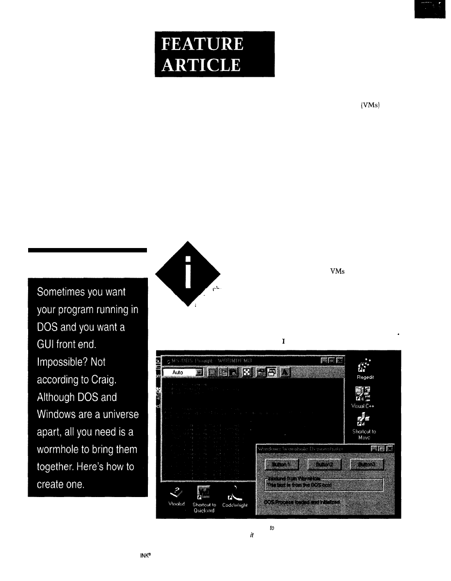
Photo 1
-As buttons are pressed, messages are senf the DOS VM in the background and displayed. When
keystrokes are entered into the DOS VM and has fhe focus, keystroke messages are sent to the Windows GUI.
26
Issue
87 October 1997
Circuit Cellar
SAVE THE DAY
Although DOS
and Windowed
applications can’t talk to each other
directly, you can create helper programs
that facilitate interprocess communi-
cations on the application’s behalf.
The easiest way to accomplish this is
with a Virtual Device Driver
In the article “Getting Beyond The
Box With Windows 95”
(INK
I
depicted the relationship between appli-
cations (including DOS
and the hardware as a three-layer pyra-
mid. The bottom-most layer represents
physical hardware (e.g., parallel ports,
serial ports, etc.)
The middle layer represents
with the specific knowledge needed to
control the associated hardware devices.
The
also sports some form of API
to communicate with the next layer up.
At the top is the applications layer,
which is the realm of DOS
and
GUI applications. The important idea
here is that both DOS
and GUI
applications can-and routinely
interact with
More specifically,
DOS
and GUI applications tend
to interact with the
same
when
using a common hardware resource.
A useful realization is that a
doesn’t necessarily have to be associ-
ated with any specific hardware. You
can fashion a
so that it’s common
to DOS
and GUI applications but
doesn’t perform any hardware interac-
tion whatsoever. With this in mind, it
was a snap to create
WORMHOLE. VXD
and cross the VM boundary.
HOW IT WORKS
The golden nugget to
W 0 RM H 0 L E
V X D's
operation is that it supports both
thestandard
API
common among Win32 applications as
well as a nonstandard API in the form
of a hook on int
so DOS applica-
tions can access the same
services.
Always remember.that
are
global across all
so every DOS box
or Windows application that uses a
wormhole’s API is communicating to
the same wormhole. This idea is what
makes the bridge between DOS boxes
possible.
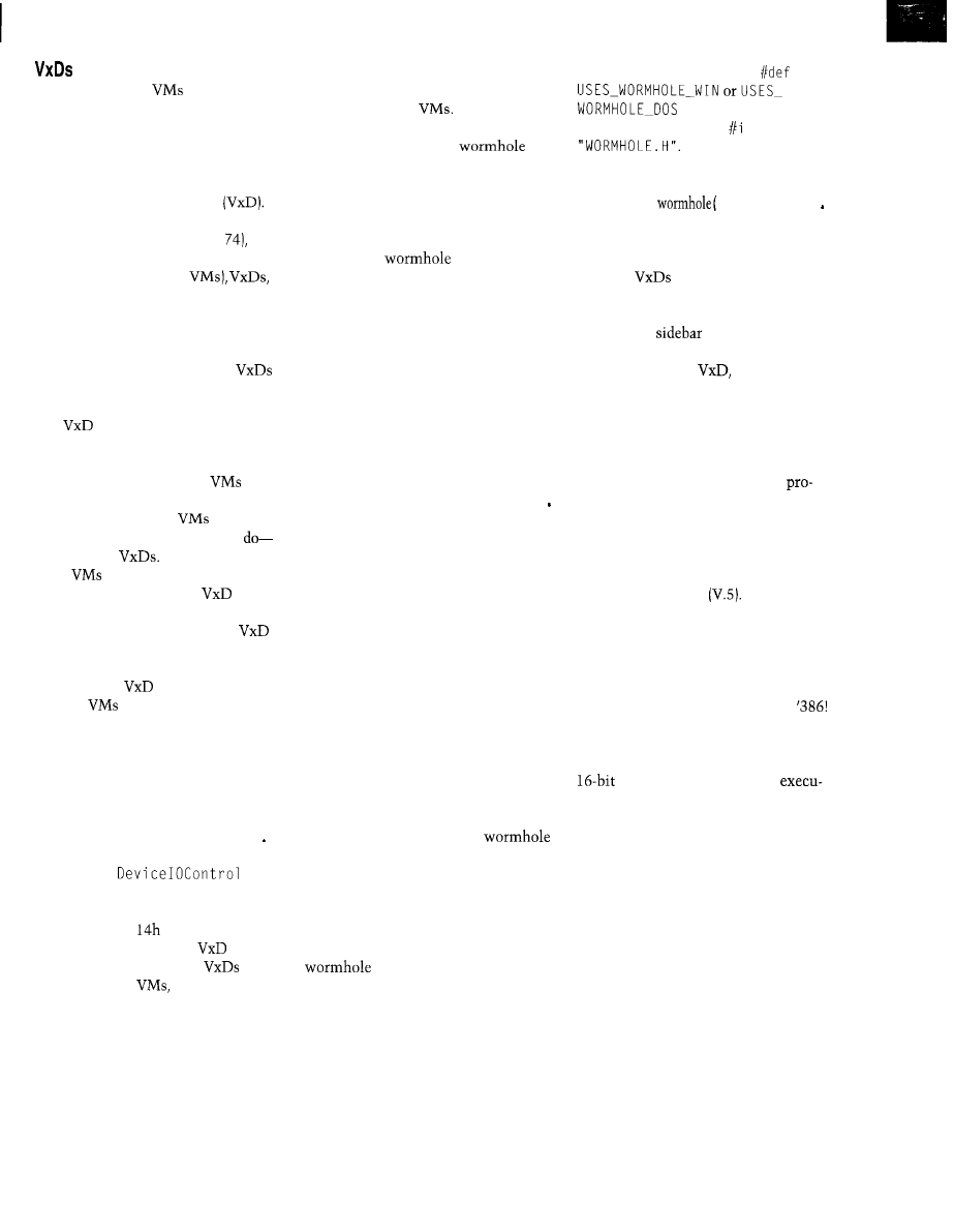
The version of
WORMHOLE. VXD
in
this article acts as a central post office
where applications can send and retrieve
messages. It can facilitate communica-
tions between up to 16 different appli-
cations across all
On startup, an application registers
itself by name with the
by
using the applicable API (listed later)
and receives a handle to its own mes-
sage queue. An application can later
use this handle like a P.O. box number
when retrieving messages coming in
through the
from other
applications. Similarly, an application
can find another application’s queue
handle and use it to send messages to
the other application.
Message sizes are limited to 250
bytes or less. Queue sizes are currently
fixed at 1 KB, which is more than suffi-
cient for most purposes.
SHOW ME!
If you’re like me, this prattle means
nothing without real source code. So, I
created a DOS executable
(W H DO S D EM
E X E)
and a Win32 application
(W H W I N
DEM.EXE)thatuseWORMHOLE.VXDto
send messages to each other. The source
code for these files will be your best
reference, as these little applications
exercise almost all the functionality of
the wormhole.
Before running
WHDOSDEM,
load
WORMHOLE. VXD
and reboot your PC
after adding the following entry to
your
SYSTEM.INI
file:
device=Cpathl\wormhole.vxd
When
W H DO S D E M
has the input focus
and a key is pressed, the character is
forwarded to
W H W I ND E M
in the form of
a message sent through the
(see Photo 1). When the message is
received by the GUI, the character is
displayed in the
I n c om i n g
box.
API
At a higher level, the API for the
is pretty much the same for
both DOS and Windows applications.
And, it supports commands that enable
applications to register themselves and
find other registered applications. The
information gleaned from these com-
mands can be used to post and retrieve
messages to and from other applications.
The API is encapsulated as static
functions in the file
WORMHOLE. H.
To
use the
Wormhol e
API, simply
i ne
(dependingonyour
target environment) and n c 1 ude
TOOLS
To build the
W 0 RM H 0 L E
V X D),
I used Microsoft Visual C 2.0
(MSVC) and VtoolsD. The combination
of VtoolsD and MSVC enables you to
program
in C, which as I soon
learned, was preferable to using assem-
bly language and the DDK. The “C
Prototypes”
has more details.
If you’re serious about exploring the
possibilities of the
I can’t more
highly recommend a better tool combi-
nation. VtoolsD also comes with loads
of documentation and several example
programs that are directly applicable to
most endeavors.
The Windows demonstration
gram(WHWINDEM.EXE)wascreated
using MSVC 2.0. Versions of the MSVC
development environment beyond 2.0
are radically different than their prede-
cessors, so I’m reluctant to upgrade to
the current revision
MSVC 2.0 generates 32-bit code that
is meant to be executed in the Windows
95 or NT environments. Though you
can create what appears to be a genuine
16-bit DOS program using MSVC 2.0,
it’s not. Just try running it on your
The
W H D 0 S D EM
application was built
with MSVC 1.6. I’ve also built it with
Borland C 3.0. These compilers generate
code, which means their
tables can run in native DOS.
REAL-WORLD IMPLEMENTATION
My most recent application for the
W 0 RM H 0 L E
came about a month ago. I
needed to give a Windows application
access to a slow (9600 bps) proprietary
network.
It just so happened that I had al-
ready created the network drivers for a
hand-held DOS portable eight months
prior.
Not wanting to create an entirely
new network driver for Windows, I
simply repackaged my old DOS net-
work drivers to take advantage of the
wormhole. Within two days, the Win-
dows application was up and running
as a network participant.
Circuit Cellar
INK@
Issue
87 October 1997
27
POSSIBLE ENHANCEMENTS
Most of the limitations of WO RMHO LE
stem from my own arbitrary decisions.
There’s no real reason, for instance,
that queue sizes have to be limited to
1 KB or that there be a maximum of 16
participants.
Also, rather than retrieving handles
to message queues and using them to
send/receive data, it may be more
convenient to use process names ex-
clusively. This technique does involve
slightly more processor overhead, but
speed isn’t a genuine issue on a mod-
ern Pentium.
Because languages other than C
derivatives have gained in popularity,
it may be desirable to encapsulate the
would allow Access, Visual Basic, and
a host of MIS programmers to benefit
from the wormhole.
HEADING ON OVER
When all is said and done, W 0 RM H 0 L E
turns out to be a convenient means of
interprocess communication among
Win32 applications whether you need
to communicate with a DOS VM or
not.
DDE, OLE, and the clipboard were
originally meant to fill this need, but
they’re more complex than necessary.
I must mention that wherever I
look in PC literature, I get the impres-
sion that the demise of DOS is immi-
nent. Heck, even palmtops are running
API within a DLL. That
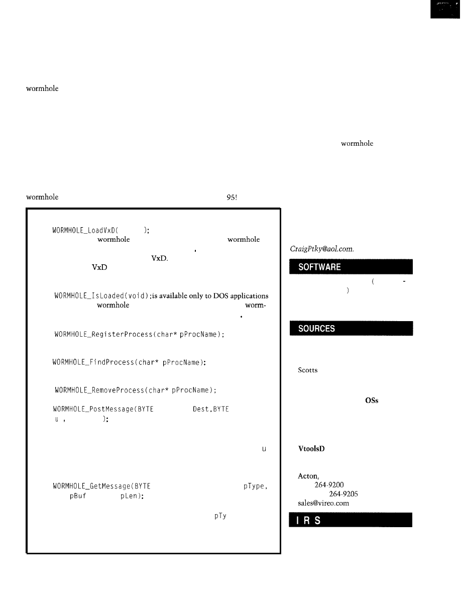
a version of Windows
C Prototypes
BOOL
voi d
is available only to Windows applications
and ensures the
is loaded and initialized. If the
hasn’t already been loaded by an entry in SY ST EM I N I, this function
attempts to dynamically load the
In dynamically loading, you must
make sure the
is in either your application’s start-up directory or in
the \ W I N D 0 W S \ S Y ST EM directory. Either way, no other API functions
will work until this function is called.
BOOL
and ensures the
has been loaded and initialized. The
hole must have been previously loaded by an entry in S Y ST EM I N I or by
a Win32 app calling the L
O
a d V
x
D API.
BYTE
registersthe
given process in the process table and returns a handle to that process. If
no room is available in the process table, it returns -1.
BYTE
looks for the given
process in the process table and returns the handle to it if found. It
returns -1 if the process isn’t found.
BYTE
removesthegiven
process and returns a value greater than
-1
if successful.
BOOL
Src,BYTE
Type,BYTE*
p B f BY T E Len
attempts to post a message to the destination-process
message queue. S r
c
should be the handle to the caller’s process queue so
the receiver may reply. You can use the Ty p e variable to describe the
application-dependent data being routed to the destination process. p B f
points to a buffer of data to be sent, and Len is the number of bytes to be
sent. This function returns TRUE if the message posted OK or FALSE if
the receiver’s queue was full or invalid.
BOOL
Dest,BYTE* pSrc,BYTE*
BYTE*
, BYTE*
attempts to retrieve a message addressed
to the Des t process handle. If a message is available, this function returns
TRUE with p S r c equal to the sender’s process handle,
pe equal to
the application-dependent type of message, p B u f filled with the body of
the message, and p Len equal to the number of bytes in the message body.
If no message is available, it returns FALSE.
Of course, in a perfect world with
no time constraints, writing software
as full-blown multithreaded Win32
applications would almost always be
preferable to cobbling together a bunch
of DOS boxes.
The reality is, however, that time to
market is more critical than elegance
of implementation.
If DOS is what the bulk of your
staff knows and a DOS/Win hybrid is
good enough to go the distance, jump
at it. I hope this
makes it
easier.
q
Craig Pataky is a systems engineer at
Hi-Tech Transport Electronics. His
eight years in software has included
everything from simple embedded
programming to operating-system
design. At present, most of his time is
spent designing and implementing
network protocols for the trucking
industry. You may reach him at
The complete source code W 0 RM
H 0 L E
. Z
I P for this article can be
downloaded from the Circuit Cellar
Web site.
Borland C
Borland Int’l.
100 Borland Way
Valley, CA 95066
(408) 431-1000
www.borland.com
MSVC 2.0, Windows
Microsoft Corp.
One Microsoft Way
Redmond, WA 98052
www.microsoft.com
Vireo Software, Inc.
21 Half Moon Hill
MA 01720
(508)
Fax: (508)
407
Very Useful
408 Moderately Useful
409 Not Useful
28
Issue
97 October 1997
Circuit Cellar INK@
Bill Jackson
Reynaldo
Compressed-Code
he growing
mand for a variety
of newer consumer and
communications products
is challenging the system designer to
find innovative ways to design more
efficiently and reduce cost. Performance
at any cost is the one and only byword
for system engineering focused on
ultimate desktop computing power.
However, cost-sensitive embedded
applications in products like cellular
phones, Internet appliances, and routers
are burgeoning. The engineering con-
centration in this particular scenario is
on balancing performance and cost.
Higher integration, smaller device
packaging, and advanced process tech-
nology are helping to reduce design
cost. To date, though, the embedded
microprocessor hasn’t contributed a
fair share.
Ideally, in this instance, the system
designer should have a compact-code
instruction set architecture [ISA) that
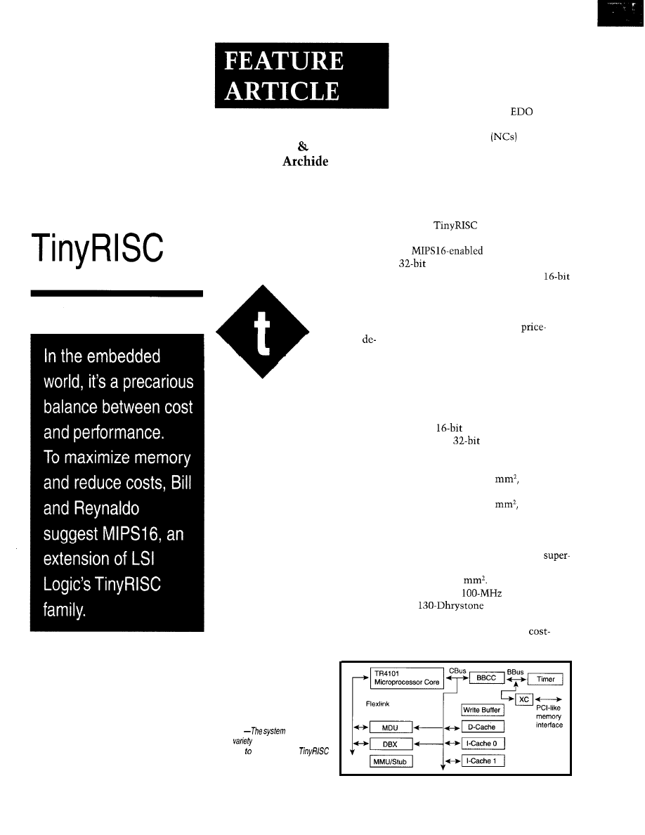
Figure 1
designer can
use a
of optional building blocks
bolted on the embedded
microprocessor core. The blocks can
be modified with customized logic.
can cut down on how much program
memory is necessary in a system.
System memory has traditionally
accounted for a major portion of the
system design cost. Conventional PCs
today require
8-16
MB of
DRAM,
for instance, costing about $50-100.
Network computers
use 8 MB of
memory, which costs about $50.
An embedded processor based on a
compressed-code ISA halves memory
size. One example is the recently de-
veloped MIPS 16 applications-specific
extension (ASE) embedded in LSI
Logic’s
TR4100 family of
32-bit microprocessor cores.
processors provide
RISC performance with an over-
all system cost more typical of a
processor. These microprocessor cores
represent the first implementation of
the MIPS 16 ISA developed by Silicon
Graphics and optimized for
sensitive applications.
The TR4100 family includes three
initial members-TR4101, TR4102,
and TR4120. Based on LSI Logic’s
0.35pm process, the TR4101 has a
clock frequency of 70 MHz and features
about 60-Dhrystone MIPS performance
running
code.
The TR4120, which includes a bus
interface unit (BIU), is a high-end
scalar machine operating at 3.3 V and
measuring 4.2
Performance is
expected to be
clock frequency
and
MIPS.
Running
code, the clock
frequency increases to 81 MHz and
70-Dhrystone MIPS performance. The
TR4101 measures 1.7
operates at
3.3 V, and dissipates 1 mW/MHz. The
TR4102 measures 1.5
operates
between 2.5 and 3.3 V, and dissipates
0.7 mW/MHz.
The TR4101 core provides embed-
ded-systems designers with a
efficient building-block approach for
30
Issue
87 October 1997
Circuit Cellar INK@
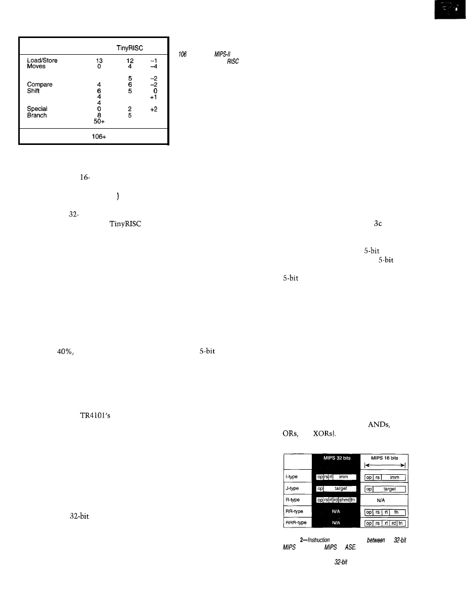
Instruction Group
MIPS-II
A
ALU
Logical
Jump
Multiply/Divide
Instructions
Coprocessor/Kernel
14
7
12 -2
4
0
- 3
0
Total
57
Table 1 --MIPS 16
reduces the number of
microprocessor instructions from the usual
found
in the
instruction set to
only 57, reducing the
code size and
memory requirements by 40%.
implementing highly integrated sys-
tem-on-a-chip designs.
It can run either
or 32-bit in-
structions on the same processor. The
Jump and Link Exchange
(J A LX
in-
struction enables the processor to
switch between
and 16-bit code.
As shown in Figure 1, the
processor core operates with a combina-
tion of LSI Logic blocks and modules,
including a basic BIU and cache con-
troller (BBCC), multiply/divide unit
(MDU), extended bus interface unit
controller (XC), timer, write buffer
(WB), and debug module (DBX).
It also has a two-way set associative
instruction or direct-mapped (I) cache
and a data (D) cache. These optional
building blocks can also be modified
via customized logic.
The processor core reduces RISC
code size by
going from over 106
instructions in 32-bit MIPS to only 57
MIPS16 instructions (see Table 1). At
the same time, it cuts system memory
requirements up to 40%.
While the MIPS16 compressed code
size is only 60% of the uncompressed
MIPS code size, the
overall
performance is equivalent to 85% of
the full 32-bit uncompressed ISA.
MIPS16 OVERVIEW
Figure 2 overviews the instruction
formats. MIPS16, which includes sup-
port for 64-bit operands, reduces the
number of 32-bit MIPS instructions by
about a third. A set of instruction
variances in this format can be ex-
pressed in MIPS
code but not in
the compressed code.
Consequently, a multiple-instruction
sequence can achieve the same effect.
The sequences are used sparingly, yet
they contribute to overall code savings.
Instruction types between the 32-bit
MIPS ISA and the MIPS 16 ASE do not
change drastically, which exemplifies
the approach taken to evolve the com-
pressed code from the current MIPS
architecture.
In the Immediate (I) type, one regis-
ter field (rt) is omitted, leaving only the
operation (OP) and source register (rs).
The remaining portion of the instruc-
tion is devoted to the immediate field.
As well, the Jump (J) type format
used for jumps and branches is nar-
rowed down in the field specifying the
target address.
The R-type is split into two related
types-RR and RRR. In each case,
fewer available bits in the 16-bit format
are used to perform some functions
previously done in the R-type.
In the MIPS ISA, 6 bits specify the
operation. Two
fields specify two
registers (rs and rt), which allow any
pair of registers to take part in this
instruction (see Figure 3a). The imme-
diate field is 16 bits wide.
In MIPS16 ASE, the operand field is
5 bits. The rt field is omitted, and the rs
is pared down to 3 bits. Therefore, one
of only eight registers can be selected,
whereas it was one of 32 in 32-bit MIPS.
Omitting the rt field means the
previous contents of a register are now
replaced with the result of the new
operation. The same thing doesn’t
necessarily happen in 32-bit MIPS. For
example, the value of one register is
increased by the immediate value in
MIPS and saved in a different register.
Operation code in the
Jump/Branch
instruction
for MIPS16 is 5 bits com-
pared to 6 in 32-bit MIPS (see Figure 3b).
The target field, which specifies a
jump or branch destination, is reduced
to 11 bits from 26.
Consequently, the number of differ-
ent kinds of branch specified in 32-bit
MIPS is curtailed. With the six-bit OP
in 32-bit MIPS, there can theoretically
be up to 64 different types of branches.
In MIPS16 with a five-bit OP, there are
less than 32.
The 32-bit MIPS 26-bit target field
permits a wide (228 bytes) range for
jumps and branches. In MIPS 16, it’s
213. If a jump needs to be further out
than this in MIPS16, a multi-instruc-
tion sequence is needed to achieve the
same effect.
As for register types, 32-bit MIPS
has a 6-bit OP, three register fields
(each could be any one of 32 registers),
and five bits for the shift amount
(SHAMT) field, which specifies in-
structions that perform arithmetic or
logical shifts. And, as Figure shows,
a 6-bit function modifies the basic
operation.
MIPS16 RR-type has a
OP,
3-bits each for rs and rt, and a
function. The RRR-type maintains the
OP and the 3 bits each for rs and
rt. However, it adds a 3-bit rd register
field, although the function field is
restricted to only 2 bits for modifica-
tion purposes.
Sometimes, instruction steps taking
32 bits in 32-bit MIPS can be directly
encoded in either the RR- or RRR-type
16-bit formats. But, there will be cases
in which a combination of instruction
steps is attempted.
However, they won’t be accommo-
dated in either RR or RRR. When that
occurs, a multi-instruction sequence
must be implemented. RR and RRR
types are used extensively for basic
integer manipulation (e.g.,
and
Figure
types are similar
the
ISA bus and
16
For example, in the
immediate-type instructions, on/y one register field is
omitted from the normal
immediate-type instruction.
Circuit Cellar INK@
issue 97 October 1997
31
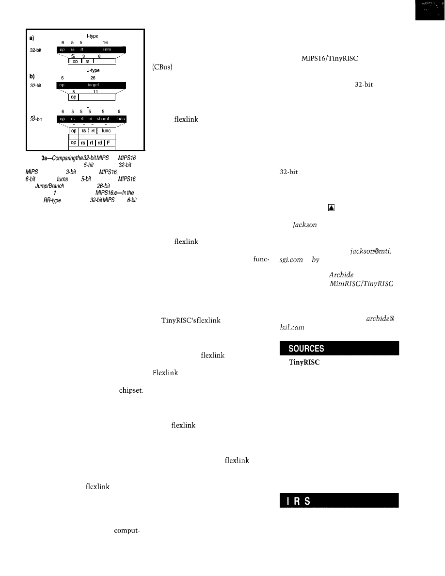
MIPS
3
MIPS16
imm
MIPS
5
MIPS16
target
Register types
MIPS
5 3 3 5
MIPS16
RR-type
5 3 3 32
RRR
-type
Figure
and
immediate-type instruction,
regisfers in
become one
register in
while a
operation
info a
operation in
b-/n
instructions, a
target field
becomes an i-bit target field in
register
instructions,
has a
operafion field and
three register fields, each of which
could be any one of 32 regisfers.
OTHER CONSIDERATIONS
Cutting back on system memory by
using a compact-code CPU is only part
of the overall solution. Other problem-
atic areas are architectural flexibility as
well as determining how reusable and
scalable an ASIC processor core can be.
A design may require additional or
different functionality for competitive
differentiation.
Here, the designer can choose from
a variety of cores and building blocks.
For example, a fast multiply/divide
unit (MDU) can be added in a commu-
nications application to perform several
modem tasks in firmware. Of course,
adding a feature tacks on more cost
savings to the design since it eliminates
a separate DSP chip or modem
Other useful functional units in-
clude peripheral controllers like ROM
or DRAM and/or video controllers and
I/O. In effect, the designer can pack
considerable functionality of various
flavors onto a design, minimizing the
amount of supporting components
needed.
A reusable RISC microprocessor
core is stripped down to only the IU
and register filer. A
interface
enables systems designers to partially
customize the CPU core, thus making
it extendable.
Next, a coprocessor interface (COP)
turbocharges the RISC core’s
ing power by enabling engineers to
tightly hook up special-purpose proces-
sors.
As well, access to the CPU bus
enables different building blocks
to be designed around the CPU. Conse-
quently, considerable latitude is pro-
vided for designing in a variety of cores
and building blocks to comply with
specific NC designs.
The
interface of the TR4101
TinyRISC microprocessor core opens
the door to the reusability feature.
This interface can extend the standard
MIPS instruction set to many other
different instructions.
Typical instructions that can be
added to the MIPS core are multiply/
add, multiply/subtract, find first set
bit, find first clear bit, and saturate
instructions, among others. It can also
be used for multiple-cycle instruc-
tions, although it’s more appropriate
for single-cycle instructions.
The
interface provides a
way to select and bolt on to the CPU
any number of designer-defined
tions (e.g., a multiplier, barrel shifter,
or pixel-manipulation engine).
This way, the systems engineer can
open up the instruction set and modify
it without changing the core processor
logic.
interface makes
this all possible. Here’s how it works.
The CPU presents two subfields of
the instruction register and rs and rt
operands at the
interface when
each instruction’s execute stage starts.
decodes the instruction, ex-
ecutes it, and writes the results back
onto the rd bus at the end of the cycle.
The CPU handles the register file
update during the write-back stage. If
the instruction needs more than one
cycle,
can either stall the CPU
via the normal stall mechanism or
write results into its own holding
registers, which need to be read later
with some user-defined
in-
structions.
MAKING THE SWITCH
Cygnus Tools will be the first of
several software manufacturers to
support the MIPS16 ASE. These tools
are based on the Open Software Foun-
dation (OSF) GNU tool chain.
Cygnus intends to provide the as-
sembler, compiler, linker, locator,
debugger, and architectural simulator
for the
architecture.
These tools will be made available free
via the Internet in early 1998.
The transition from a
MIPS
development environment to that of
MIPS16 is made simple. The software
developer can begin with a 100% MIPS
application and convert the routines to
MIPS16 step by step.
Compilers, linkers, and debuggers
have full support for both instruction
formats. Basically, a flag to the com-
piler controls whether it generates
MIPS or MIPS16 instructions.
The remainder of the code-development
process (i.e., linking and debugging) is
the same for both MIPS, MIPS16, and
mixed binaries.
Bill
is the marketing manager
for embedded applications at Silicon
Graphics-MIPS Technologies. You may
reach Bill by E-mail at
or phone at (415) 933-7368.
Reynaldo (Rey)
is the product
manager for the
line of microprocessor cores at LSI
Logic. He has also held positions at
Toshiba, NEC, Zilog, and Philips. You
may reach Rey by E-mail at
or
by
phone at (408) 433-7987.
TR4100 family
LSI Logic
155 1 McCarthy Blvd.
Milpitas, CA 95035
(408) 4338000
Fax: (800) 457-4286
www.lsilogic.com
MIPS16 ASE tools
Cygnus Solutions
1325 Chesapeak Terrace
Sunnyvale, CA 94084
(408) 542-9600
Fax: (408) 542-9699
www.cygnus.com
410 Very Useful
411 Moderately Useful
412 Not Useful
32
Issue
87 October 1997
Circuit Cellar
INK@
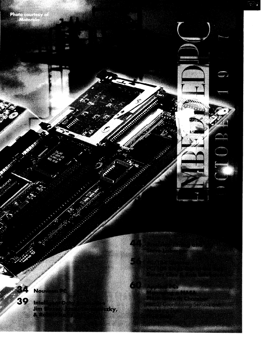
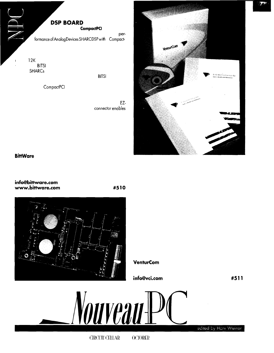
Snaggletooth
is the industry’s
first product to combine the fast floating-point
a
PCI form factor. The 240-MFLOPS card features a pair of
40-MHz ADSP-2
106x
SHARC processors, each including 2
or 4 Mb of on-chip dual-ported SRAM. The board also features
up to 5
x 48 bits of zero-wait-state SRAM, four external link
ports, and a
mezzanine site for off-the-shelf I/O interfaces.
The two
share a common processor bus, giving each
processor access to the optional bank of SRAM,
mezzanine
I/O devices, and the internal SRAM of the other processor.
Snaggletooth
is supported by source-code devel-
opment tools, including Analog Devices’ SHARC-ANSI-compliant
compiler, assembler, linker, simulator, and source-code debugger.
True real-time in-circuit emulation is available with the optional
ICE emulator. An IEEE 1 149.1 -compatibleJTAG
nonintrusive DSP control and debug. The DSP21 k Toolkit also
provides developers with C-callable host I/O functions, DSP
functions, example code, and diagnostic utilities under Windows
95, Windows NT, and QNX operating systems. A DSP2 1 k Porting
Kit is also available to facilitate Snaggletooth support on additional
platforms and operating systems.
The Snaggletooth CompactPCl
sells
for $5595.
Research Systems
33 N. Main St.
Concord, NH
03301
( 6 0 3 ) 2 2 6 - 0 4 0 4
Fax:
(603) 226-6667
APPLICATION DEVELOPMENT SOFTWARE
Component Integrator
is an easy-to-use development tool
for integrating, configuring, and building dedicated Windows NT
target systems. Its optional OS extensions-Embedded Compo-
nent Kit (ECK) and Real-Time Extension (RTX)-provide vital capa-
bilities for real-time and embedded operations for Windows NT.
System developers can integrate custom applications, COTS
software, ECK, and RTX extensions with Component Integrators’
knowledge base of Windows NT components. An easy-to-use
graphical interface simplifies selection and configuration of soft-
ware components. A bootable target can be built on disk or flash
media, or an installation image can be produced that can be
loaded onto a target from a network server or CD-ROM.
Component Integrator reduces target-system size by enabling
the developer to choose only the Windows NT components
required for the application. Typical uses include industrial control,
telecommunications, and medicine.
Pricing for Component Integrator starts at $9500.
215
First St.
l
Cambridge, MA 02142
(617) 661-1230
l
Fax: (617) 577-1607
l
www.vci.com
34
INK
1997
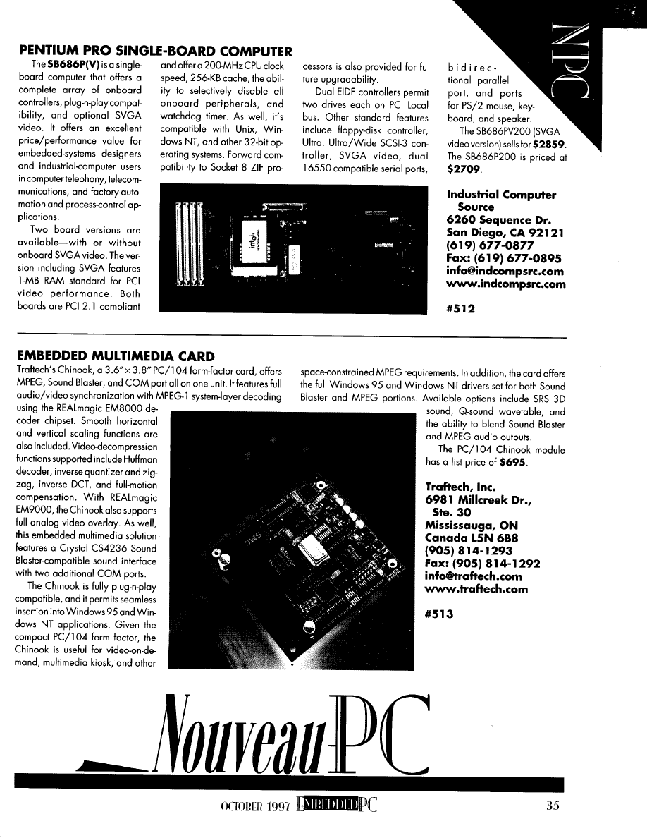
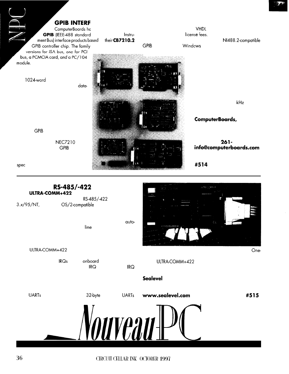
All versions use this new chip, which
features a high-speed state machine
and
FIFO to implement fast
transfer rates. Maximum sustained
transfer rates are greater than 1 MHz
with 4-m cables and exceed 1.5 MHz
with shorter cables.
The CB72 10.2 chip is one of the few
IEEE-488.2~compliant talker/listener/
controller chips available. Designed
entirely in VHDL code, the chip imple-
ments the
state machine defined in
the specification. Since it is backwards
compatible with the
(com-
monly found on older
interface
cards), replacing this chip with the
CB72 10.2 brings that board up to new
compliance. The chip is priced as
ACE FAMILY
IS
introduced a family of
General-Purpose
on
includes the chip, three
low as $8 in quantity, and
purchase with low-cost
All boards are bundled w
library for DOS,
source code is available for
ith a complete
3.1, and Windows 95, ensuring
functional compatibility with popular
languages and applications. The
boards are also supported by a vari-
ety of third-party software, including
HP VEE and Test Point.
The boards each list for $299. A
low-cost ISA version that eliminates
the FIFO or high-speed state machine
and has a maximum sustained data
transfer rate of 300
sells for
$ 1 9 9 .
Inc.
125 High St., Ste. 6
Mansfield, MA 02048
(508) 261-l 123
Fax: (508)
1094
www.computerboards.com
AUTOMATIC
CARD
The
is a serial I/O adapter for the IBM
PC and compatibles. It provides four
DOS, Windows
QNX, and
serial ports with the
ability to connect up to 3 1 RS485 devices to each port.
The OS views each DE-9 port as a COM port, so the standard
COM driver can be used for RS-485 communications. Its
initialization circuit enables the RS-485
driver during character
transmission and disables it afterward. The adapter lets the RS485
line be managed transparently without user or software interven-
tion and eliminates RS-485 network contention.
The
supports the RS-422 specification,
providing long-distance (4000’) communications and noise immu-
nity. User-selectable AT
and an
interrupt status port
let the user set each port to a separate
or share a single
over multiple ports. A versatile range of address settings provides
seamless integration into existing systems.
The card supports standard PC data rates up to 460.8 kbps,
providing support for ultra-high-speed serial applications. The
16550
are standard. The new
FIFO 16650
and 64-byte FIFO 16750 UARTs are available as options.
and two-port versions are also available.
The
sells for $369 ($319 without the
automatic circuit).
Systems, Inc.
P.O. Box 830
l
liberty, SC 29657
(864) 843-4343
l
Fax: (864) 842-3067
EMBEDDED MODULE
The
provides all the functionality of a
single-board computer in a 240-pin surface-mount component, plus a
preloaded BIOS, embedded ROM-DOS, and an internal resident flash
disk. The module includes ail standard motherboard features, including a
40-MHz
CPU,
DRAM, IDE hard-disk controller, and
drive controller. It also has two serial ports, a bidirectional parallel port, full AT
keyboard, speaker interface, real-time clock, watchdog timer, full ISA (PC/l 04) bus,
and 256 KB of user-available flash memory.
The
is a multichip module containing more than 80 components. The
240-pin package is used to bring out the standard I/O connections. There are no
licenses to negotiate. Powering up the
results in a DOS prompt. A
development board is available to facilitate testing software on a target CPU.
Pricing for the
starts at $104 in OOO-piece quantities.
ZF
Inc.
1052
Ct.
Palo Alto, CA
94303
( 4 1 5 ) 9 6 5 - 3 8 0 0
Fax:
( 4 1 5 ) 9 6 5 - 4 0 5 0
www.zfmicro.com
Arcom’s SBC IO4
single
board
computer is
complete with
fully-licensed ROM-DOS 6.22 pre-loaded into
on-board Flash memory.
l
3865X-25 or
l
ROMDOS Flash Filing System
l
Mb Flash 2Mb
standard
Interface
3 year
l
5 year Product availability
Arcom’s wide range of PC/ IO4 modules:
l
Digital
l
Multi ADWDAC
l
Multi-relay
l
II
Free: 888-94 I-2224
8
I-7807
Fax-on-Demand: 800-747-I 097
E-mail:
Web:
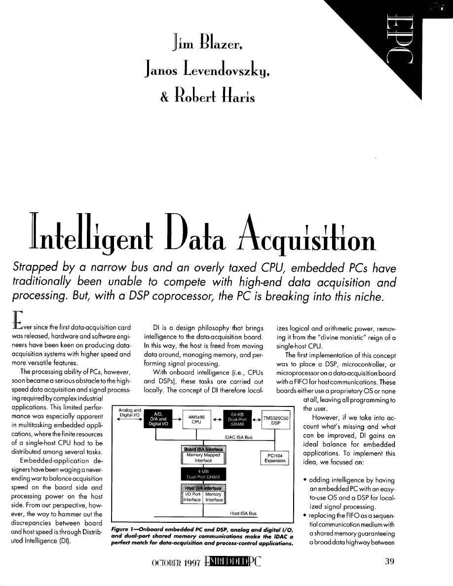
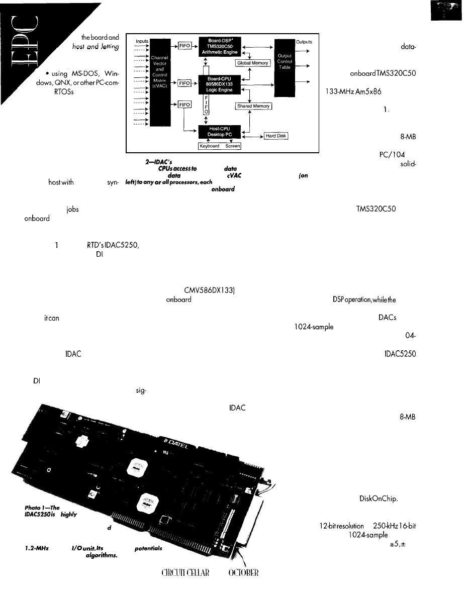
the CPU read only
required data
patible
running on the
board’s CPU
l
enabling hierarchical or paral-
lel processing by having ana-
log inputs available to all the
system processors
l
providing a direct communica-
tion path between all system
processors
Figure
unique processing and communication architecture
l
enabling multiple boards in a
gives three
acquired
in concert, providing parallel
single
multiboard
or hierarchical
processing. The
mofrix sends inputs
the
performing its own algorithm. Outputs
(on the right) are controlled by
processors.
chronous A/D conversions
Since different
can be assigned to the
CPU and DSP, the hardware
structure is flexible enough to mirror the
object-oriented structure of the software.
Photo presents
a
board implementing the concept. It’s a
highly intelligent signal-processing card
that includes an embedded PC and DSP,
shared memory, multiboard sync clocks and
triggers, and an advanced analog unit. Its
hardware potentials are extended by so-
phisticated algorithms. With these capa-
bilities,
serveatthecoreofa PC-based,
high-speed industrial controller operating
under Windows.
Let us illustrate more of the DI concept by
examining the
board in further
detail.
W H A T I S I D A C ?
brings intelligence closer to the places
where data is acquired and real-time
a
intelligent signal process-
ing card featuring an embedde
nal processing is needed. It increases system
performance by sharing tasks optimally
between the different signal-processing
units. To implement intelligence on IDAC,
several areas of technology were needed:
l
leading-edge versatile analog front end
(e.g., ADA3400)
l
advanced embedded CPU technology
(e.g.,
to serve as an
logic engine
l
DSP coprocessor technology implemented
as an arithmetic engine that provides the
necessary computational power to per-
form sophisticated real-time digital sig-
nal processing on the collected data
l
shared and global memory to help cre-
ate large, flexible and parallel access
from both the host and board sides. A
direct-host FIFO is included for DSP com-
munications.
l
shared memory and direct serial commu-
nications for multiple
installations
in a single host running Windows
PC, DSP, shared memory, multiboard
sync clocks and triggers, and an odvonced
analog
hardware
ore extended by new
To integrate these components
in versatile and intelligent
acquisition and control systems,
RTD designed the IDAC5250
with an
fixed-point DSP unit and a
CPU. The
skeleton of the IDAC5250 is
illustrated in Figure
The processor’s internal
cache and floating-point pro-
cessor is coupled with
DRAM, serial and parallel ports,
watchdog timer,
ex-
pansion bus, and flash
state disk with Windows and
DOS compatibility. Thus, it pro-
vides a versatile embedded PC
for data acquisition.
Texas Instruments’
board
DSP-the arithmetic engine-provides
64K words of zero-wait-state program
memory, 32K words of zero-wait-state lo-
cal data, and 32K words of one-wait-state,
hardware arbitrated global data memory.
All DSP memory, including DSP internal
memory, is mapped into the board-CPU
extended memory. Hardware-arbitrated ac-
cess to the global data memory assures
uninterrupted
board
CPU reads or writes the global memory.
The ADC and all three
have
independent FIFO buffers to
process burstydata. Theonboard PC/l
bus connection between board CPU, DSP,
and analog I/O unit enables the
to function as a stand-alone machine. How-
ever, its architectural strengths become
clear when placed in a host computer.
In contrast to FIFO communications, the
4 MB of hardware-arbitrated shared memory
enables simple and fast communication
between the CPU and host. With its
DRAM, the CPU can run DOS, Windows,
QNX, and other operating systems requir-
ing DOS compatibility.
This relatively large memory also sup-
ports high-speed data-acquisition applica-
tions when the collected data is streamed
into the memory. A 32-pin solid-state-disk
socket supports flash, SRAM, or large flash
drives like M-Systems’
The
analog
I/O features 16 single-ended
and 8 differential input channels with
1.2MHz
or
resolution and the
FIFO. The
programmable input ranges are
10,
or O-l 0 V, while programmable channel
40
INK
1997
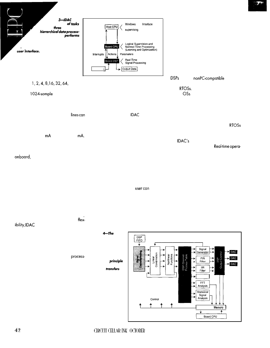
Figure
pro-
vides a
division
,
between
processors
in
ing, where the DSP
real-time signal analysis, the em-
bedded PC handles learning and
optimization, and the host provides a
User
for
parameter setting and
the application
Critical signals
for display
Initial Parameters
Input Data
gains are
and 128.
S I G N A L P R O C E S S I N G
The three analog voltage outputs with inde-
pendent
FIFO buffers pro-
vide high-speed analog feedback.
The digital control is implemented in an
EPLD that has one 8-bit I/O port and eight
bit-programmable DIO lines. These
generate an interrupt when a bit-or com-
bination of bits-either changes value or
matches a programmed value. The buffered
lines can sink 24
and source 12
SIGNAL PROCESSING HIERARCHY
With locally implemented intelligence
an intelligent data-acquisition
board can multiply the performance of a
single host.
This increased performance is most
apparent when performing hierarchical
signal processing (HSP) and automated
reasoning while preserving real-time op-
erations at high sampling rates.
With IDAC5250, these capabilities are
ensured by
the
various signal paths summa-
rized in Figure 2. As you see, there are
several possibilities to assign processing
Signal-processing power often proves to
be the bottleneck of embedded industrial
applications. When intelligence is involved,
optimal performance depends on how tasks
are distributed among processing units.
Taking advantageof
modular hard-
ware structure, the board can work in the
hierarchical order shown in Figure 3. First
of all, the DSP is engaged with real-time
signal processing, and if an event requires it,
the DSP sends an interrupt to the board CPU.
The board CPU supervises the applica-
tion and takes necessary actions when inter-
rupts arrive from the board DSP. Besides
supervising theapplication, the board CPU
does nonreal-time processing (e.g., learn-
ing and parameter optimization) when fast
computations aren’t needed.
The host CPU offers an easy-to-use inter-
face under Windows. The
then set
the parameters for a concrete application.
These parameters are loaded from the
host to the board. In case a particular event
occurs in the course of running the applica-
tion, the host receives the collected or
unit, respectively, and displays it under
Windows.
The user can then receive information
explainingwhya particulareventoccurred.
After detecting critical instability in PID con-
trol, for example, the signals of a control
loop might be sent to the host CPU for
further analysis.
O P E R A T I N G S Y S T E M
Intelligent data-acquisition boards with
alone or
micropro-
cessors exclude the use of DOS, QNX, or
other
But, DOS and other PC-com-
patible
offer some advantages since
users can use their favorite desktop-PC com-
piler and debugging tools.
Running the same operating system on
the target and development systems makes
it easy to port the developed application
program to the board. And, many
provide built-in networking and multitasking.
While it’s possible to run Windows on
the
CPU, it offers poor real-time
multitasking performance.
tion stipulates acting deterministicallywithin
a given length of time.
Windows simply doesn’t provide real-
time performance when events follow each
other in millisecond range with no assurance
that they’ll ever be processed. Obviously,
the
fast data acquisition and high sampling
rate of real-time digital signal processing
aren’t conceivable under Windows.
Nevertheless, you can take advantage
of Windows’ graphical features. The host’s
user-friendly interface can supervise an
application, set initial parameters, and
units to the collected data. Given this
processed data from the analog or DSP
display the obtained dato offline.
is capable of HSP.
HSP ranks one processing unit above
another to perform automated reasoning.
Information is passed from a lower layer to
a higher one in a more condensed and
abstract form.
Figure
multi-
This feature is a great aid to
control engineering when a huge amount
of observed data is to be converted into a
few logical variables (regarding the qual-
ity of control). Based on these logical vari-
ables, a control action needs to be taken.
HSP ensures the mapping from raw
data into abstract categories (e.g., the
state of the system and quality of control)
for these applications. The classic example
is condition-based maintenance that moni-
tors the state of complexelectromechanical
systems.
&king library en-
ables the user to call
D S P o p e r a t i o n s
without
program-
ming the DSP and
to perform multiple
tasks.
This
is implemented by
dynamic
of
control that ensure
the execution of the
different tasks.
PID
Global
1997
REAL-TIME MACHINE
Missioncritical and complex
tions frequently require real-time operations
that usually lie beyond the capabilities of
traditional DOS and single CPU embed-
ded systems.
To turn
into a real-time machine,
the designers took advantage of the rela-
tively high speed of the DSP compared to
the CPU. In other words, the DSP carries out
the real-time processing.
To enable the user to exploit the
processing power without having to get
into the details of assembly programming,
two approaches were pursued.
First, single-task DSP operations let the
user run single applications on the DSP
(e.g., filtering, FFT, etc.). In this approach,
DSP operations are activated by function
calls in the user program. These C calls
activate ready-made programs (written in
assembly language), which are loaded into
the DSP program memory with the proper
parameters and executed.
As
well, a multitasking function library
was written for the board DSP. The user can
therefore call DSP operations without pro-
gramming the DSP and perform multiple
tasks, if the tasks can be accommodated in
a time frame.
This principle is implemented
by
dynamic
transfers of control that ensure the execu-
tion of different tasks. Figure 4 depicts the
structure of the multitasking approach.
To exploit the advantages of a
fledged RTOS (i.e., notonlymanaging tasks,
but also managing CPU, memory, timer,
interrupts, DMA, and networking), run QNX
or another real-time system on an IDAC. If
you decide to emphasize networking, you
can combine the signal-processing power
of many
DISTRIBUTED INTELLIGENCE NOW
Real-time data acquisition and control
using the most popular GUI-Microsoft
Windows-mandates special hardware
adaptations. Traditional passive data-ac-
quisition boards require constant and im-
mediate host intervention. Faster buses,
such as PCI, create an additional process-
ing burden and do not improve real-time
data acquisition and control.
This dichotomy brought us to the dawn
of for the PC. Data-acquisition boards
with
embedded PCs and open
that provide real-time processing power
nate this environment.
Se-
ries
illustrates the possibilities
for new data-acquisition products as we
embrace and make Windows the opti-
mum data-acquisition and control platform.
The international hardware and
design team
Hazel, Dr.
Dr.
Dr. Josef Goal,
and Paul Ganter. Financial
assistance was provided by the Ben Franklin
Technology Center, State College, PA.
As director of engineering at Real Time
Devices USA, Jim
manages a multi-
national engineering team designing intel-
ligent data-acquisition hardware and
ware and embedded DOS-based comput-
ers. He a/so serves as a director of the
PC/I 04 Consortium, secretary of the IEEE
P996. Technical Committee,
and
chair of
the PC/I
may reach
Jim at
Dr. Janos levendovszky is director of
USA BME laboratories in Budapest, Hun-
gary, and Szechenyi Professor of Electrical
Engineering at Technical University of
Budapest. He teaches communication
theory, adaptive signal processing, and
neural
theory and conducts re-
search on neuralnetworks, signaldetection
theory,
statistical resource management, and
CAC for ATM networks. You may reach
Janos at
bme. hu.
Robert Haris, president and CEO of Real
Time
Devices USA, spent 25 years as a
Boeing senior aerospace engineer and
international business consultant before
coming to
RTD
in
1990.
He defined the
architecture and structured the multi-
national task force.
REFERENCES
Real Time Devices USA,
State
College, PA, 1997.
Real Time Devices USA, Introduction to
PA, 1997.
SOURCES
Real Time Devices USA,
200 Innovation Blvd.
State College, PA 16804-0906
(814) 2348087
Fax: (8 14)
18
413
Very Useful
4 14 Moderately Useful
4
15
Not Useful
ISA slots
The
motherboard
combines quality and
affordability with an industrial
design to meet your needs.
Seven full length ISA slots
ensure expandability for the
cards that you use.
Our engineering staff will
gladly discuss custom
motherboard designs. FCC
UL certified systems are
also available.
l
Six
full length 16-bit
ISA, One
shared
slot
l
Intel, AMD SGS-Thomson
486 CPU
support
l
VIA
l
Up to 64MB RAM, 256KB cache
recision
an
When
precise timing of events is required,
is not the way to go since
each call to the clock a/so takes up time. Steve therefore moves this operation
into the hardware and gains better than
resolution.
e live in an asynchronous world.
Things happen when they happen. And,
now that we’ve abandoned the simplicities
of DOS for operating systems like Windows
NT, Windows 95, and Linux, asynchrony
has taken over the world of computing, too.
Although we’vegained additional power
with these operating systems, it comes with
a loss of control over when things happen.
And, it creates a new class of problems for
timing asynchronous events.
THE TIMING PROBLEM
How can we measure the time intervals
between events? For timing external events,
the traditional strategy is to use a real-time
clock. The clock is programmed to count
port and stores it for later data analysis.
know of one board that includes a tiny FIFO
so up to four events may be stored if the
software responds slowly to the interrupts.
An elegant solution to the external-event
timing problem is the PC board presented in
Photo 1 and Figure 1 (complete schematics
available on Web site). It precisely tracks
the times of incoming TTL pulses without any
intervention by application software, oper-
ating system, bus, or CPU. To make the
board maximally independent, it hasenough
memory to store the times of many pulses.
I use this timing board in this article.
For timing software transactions, the
task is a little moredifficult. It’s simple
c 1 oc k
at the beginning and end of a
transaction and measure time as the differ-
ence, but this technique provides only
1
0-ms
resolution. Plus, Heisenberg’s uncertainty
principle is at work here.
Almost any method of timing software
takes time. cl
k
has as little overhead
as you can expect. On my
tium, it takes an average of 320 under
Windows 95 (range 307-420) and 71
under Windows NT 4.0 (range 65-158).
Bettertemporal resolution and (in Windows
95) less interferencerequireanothersolution.
An ideal solution to the software-timing
problem would present time in microsec-
onds at a 6-byte memory-mapped port. This
would allow microsecond timing for up to
withoutoverflowing thecounter
input line.
The interrupt service
routine collects the cur-
rent value of the hard-
ware timer at an I/O
44
ISA-bus boord
two
connectors for inputs and outputs.
process could time
INK
1997
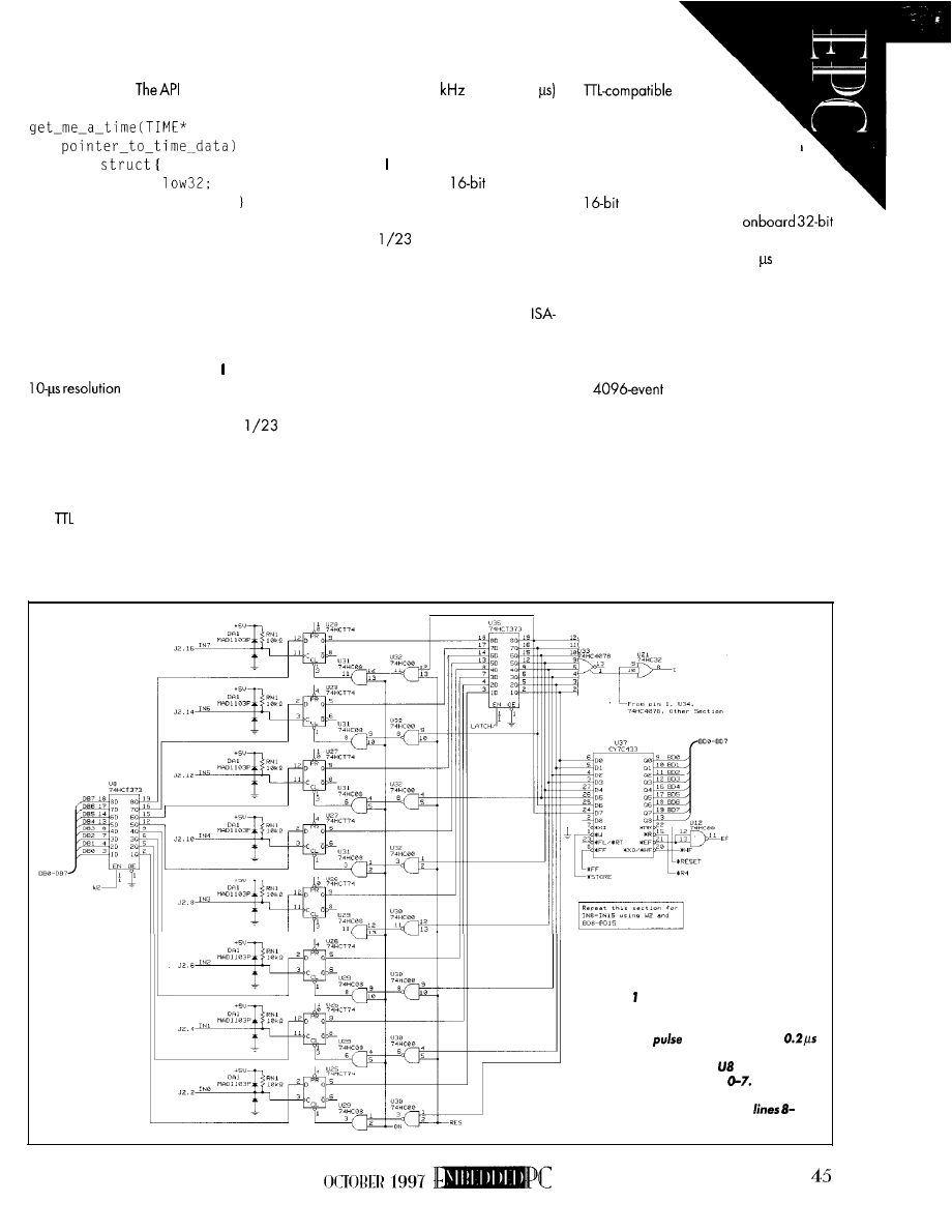
itself and report the results to a central data
analysis program.
could simply be:
t y p e d e f
u n s i g n e d l o n g
u n s i g n e d s h o r t h i g h 1 6 ;
TIME;
The timing board enables a solution to a
software timing problem that falls only
slightly short of this ideal.
S O L U T I O N E V O L U T I O N
As a neuroscientist, I faced this general
timing problem in 1981 when needed
in timing intervals between
electrical events given off by brain cells.
In the lab, we were using a DEC 1
for real-time data acquisition and experi-
ment control. The CPU’s slowness was the
main problem. I used a Schmitt trigger to
convert the electrical activity of nerve cells
into
pulses, but the pulses had to be
timed by the computer.
The obvious solution of counting time in
an interrupt handler for a real-time clock
board was impractical because interrupts
occurring at even 10
(every 100
dominated the CPU and precluded acquir-
ing any analog data or using the computer
to control the ongoing experiment.
In 1981, solved this problem in a
makeshift way, using a
parallel I/O
board to communicate with an external
logic circuit. Over the years, as we moved
from the 1
to the 80x86 PC, the
solution has evolved into a system that still
implements the 198 1 strategy but is easy to
use and readily available.
The system comprises a full-length
bus timer board that uses 16 bytes of I/O
port and one IRQ to communicate with ‘x86-
or Pentium-based PCs. Software libraries
and drivers enable rapid development of
applications for microsecond timing of ex-
ternal events or software transactions un-
der DOS, Windows 95 or NT, and QNX.
T H E H A R D W A R E
The design principle of the hardware is
to keep precise time without any intervention
from the CPU, bus, operating system, or
application software. The timer board has
16 inputlines, each individuallytriggerable
by the rising edge of a
pulse.
The hardware guarantees
temporal precision by storing a
32-bit time whenever a pulse occurs on
one of the input lines. It tracks which line
or lines registered a pulse
by
associating a
mask with each 32-bit time. The
timing is based on an
counter, and timer resolution is software
selectable in decades from 1
to 10 ms.
The board registers time without any
intervention, but software is necessary to
acquire the data from the timer board. For
precise timing of many successive events
without high-priority software intervention
to read times, the timer hardware contains
a
FIFO.
Thus, the software that reads times can,
with some knowledge of the average and
maximum event rates, check the hardware’s
status frequently enough to empty the FIFO,
but infrequently enough so that system
performance isn’t compromised.
T I M I N G E X T E R N A L E V E N T S
One potential user of the board was
trying to understand the source of noise on
Figure a--The input pulse sensing logic
uses a double buffer of D-latches to
mediate race conditions that could arise
if an input
arrives during the
when the previous set of pulses is being
stored
into the FIFO.
is the enable
register for input lines
The logic in
this diagram shows only input
lines D-7
and gets repeated for input
15.
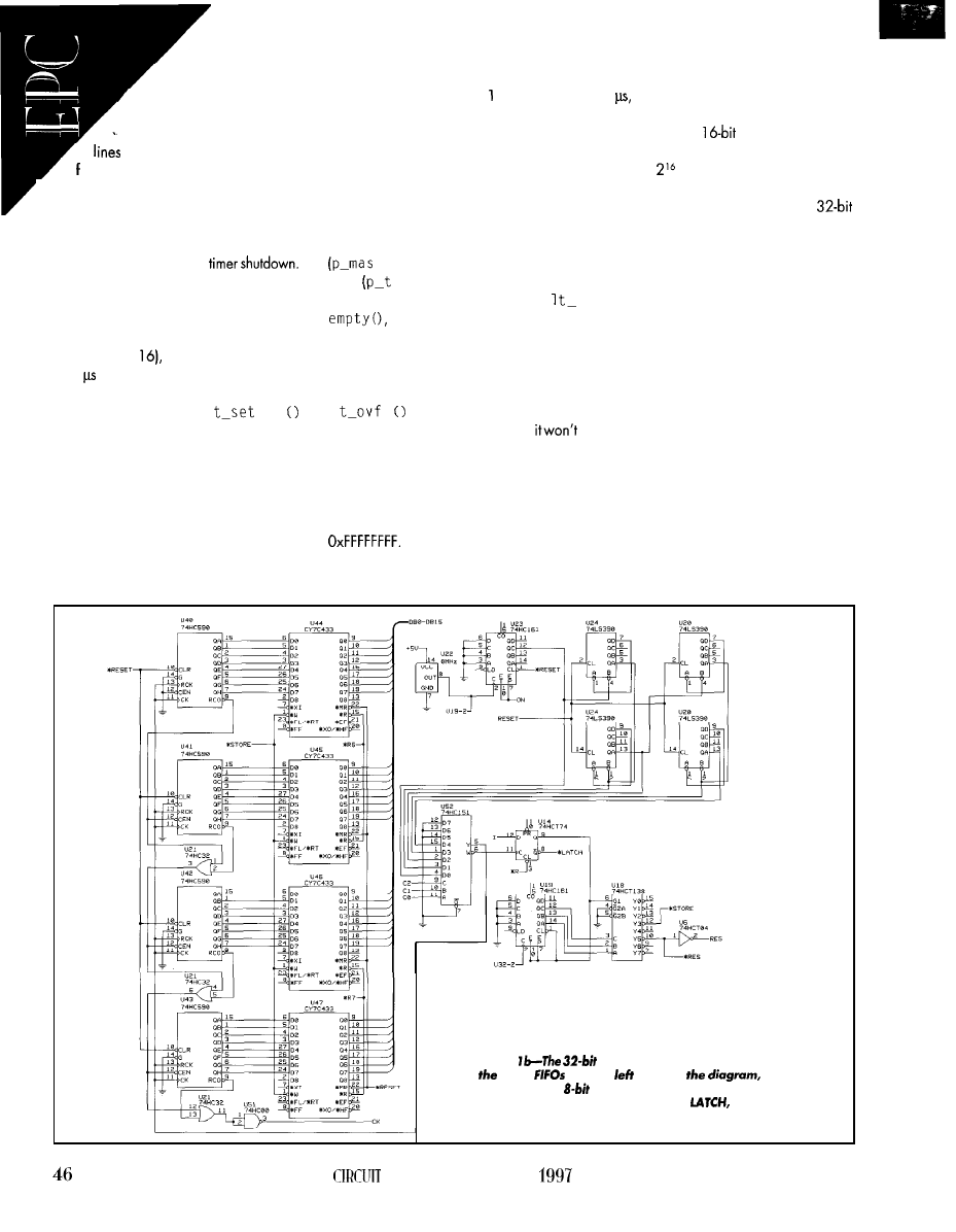
a set of 16 slip rings
and wished to assess the
reliability of the signals. He
wanted to time pulses on 16
with microsecond precision
.
or a period of 30 days or longer.
The application code in listing 1 is a
thread he could use in Windows NT or 95
to set up the timer board and collect the
data. The thread has three phases-timer
setup, data collection, and
Timer setup initializes the softwaredriver,
issues a hardware reset to the board, selects
the use of library mode 0 (the board-level
interface), enables the requisite input lines
(in thiscase, all
sets the timer resolution
(to 1 here), and starts the timer.
To run under DOS, no driver is needed.
Under Windows NT or 95,1
up
returns a handle to the driver.
Many different application programs
can have separate handles to the driver
simultaneously, and a separate handle must
be created for each thread in a single
application. Onlysingleboard installations
are currently supported, but this restriction
can be relaxed with simple revisions of the
Data collection occurs in a w h i 1 e loop
that repeatedly sleeps for s, checks the
timer board status to determine whether the
hardware counter has overflowed in the
In the application outlined here, each
iteration of the datacollection loop retrieves
last second, and then attempts to retrieve
up to 100 events every second. The events
are returned in twoarrays-unsigned shorts
events from the FIFO.
k) for the masks and unsigned
longs
i me) for the times.
The data-acquisition function,
returns the number of events
that were available on the FIFO, up to the
size of the request given as the last param-
eter of the calling sequence.
If the counter overflows, then a call to
1
1
returns TRUE. Internally, the
overflow indicator is set to FALSE so
be TRUE until the counter overflows again.
This approach works because the hard-
ware counter sets the overflow bit in the
status register, resets the counter to zero,
and keeps counting when it reaches
The need to count overflows
depends on the duration of each timing run
For example, with a timing resolution of
1
the 32-bit counter on the timer board
overflows about every 72 min. If overflows
Simple but careful programming is
are counted in a
short, then time can
needed to determine whether the
times registered near the time of counter
overflow occurred before or after the actual
be registered with microsecond precision
overflow. But, there are no ambiguities as
for over
h (i.e., 4 years).
long as the data-collection loop sleeps for
only seconds or minutes between attempts
to empty the timer board’s FIFO.
Timer
shutdown isaccomplished
by
stop
ping the timer board, emptying the last
events out of the FIFO, resetting the board,
and closing the connection to the software
driver.
In the toy
application
shown in Listing 1,
the program exits the data-collection loop
after 5000 events occur and executes the
shut-down code sequence.
In a real application, thedatacollection
loop may be allowed to continue indefi-
nitely. Then, timer shutdown should occur
in a routine that’s called when the program
software libraries.
and the timing resolution used.
is exited.
Figure
counter on the timer board, shown with
time
on the
side of
is built by
cascading four
counters. The logic on the right side of the
diagram generates sequentially the
STORE, and RES
pulses to control the operation of the event double buffer.
CELLAR
INK
OCTOBER
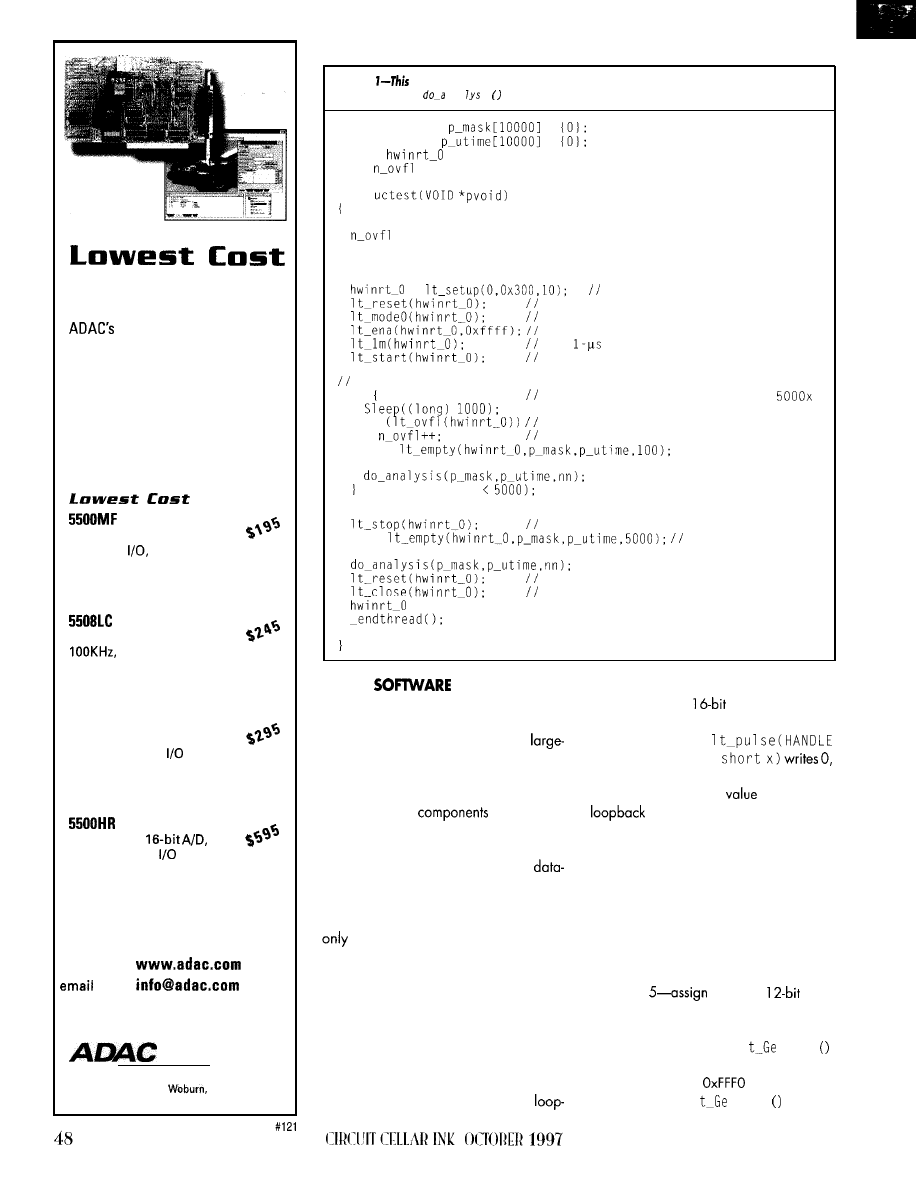
Data Acquisition
new Value-line has
uncompromising design features
and high quality components at
prices below the low cost guys!
Just check out the specs:
8
channels 12-bit A/D,
16 digital
Counter/Timer
H i g h S p e e d
8 channels IP-bit A/D,
DMA
M u l t i - F u n c t i o n D M A
5516DMA
16 channels 12-bit A/D,
DMA, 16 digital
H i g h R e s o l u t i o n
16 channels
DMA, 8 digital
learn more:
voice
800-648-6589
fax
617-938-6553
web
American Data Acquisition Corporation
70 Tower Office Park,
MA 01801 USA
Listing
complete thread can be used with existing software libraries to get data from
the timer board.
na
is
is the user’s function for analyzing and storing the timer data.
unsigned short
=
unsigned long
=
HANDLE
= NULL:
long
= 0:
long n-events = 0;
void
int nn;
= 0;
n-events = 0;
//Timer setup
=
get handle to driver
reset timer board
set mode 0
enable all input lines
set
resolution
start
Collect data
do
sleep 1 s, ask for data, repeat
if
check for an overflow
read up to 100 events from FIFO
nn =
n-events += nn;
while (n-events
//Timer shutdown
stop board
nn =
get all events
n-events += nn:
reset timer board
= NULL;
close driver
return;
TIMING
TRANSACTIONS
Another user wanted to achieve 100-p
resolution in timing both the client and
server software transactions on a
scale client-server system for Windows NT.
Figure 2 shows the organization of the
hardware and software developed for this
application. The
are the timer
board, a dynamic linked library (DLL) with
shared memory to assign each software
client a unique ID number, and the
acquisition application to retrieve the events.
Although one server and many clients
write events to the timer board’s output port,
one application reads data. The board
and the Windows NT (and 95) drivers work
well in this shared mode, but nonsense
results if multiple processes read events.
The software timing application takes
advantage of 16 lines of TTL output avail-
able at a connector on the timer board. To
convert software events to hardware trig-
gers, these output lines are connected to the
timer input lines by o 40-pin flat-cable
backconnector. The state of the output lines
is controlled by o
write-only I/O port
within the timer board’s address space.
A single call to
hwinrt, unsigned
x, 0 to theoutput port, causing brief pulses on
the lines specified by the
of x. With the
connector in place, this triggers
the timer’s inputs and registers an event.
The code for the DLL appears in Listing 2.
This implementation of the DLL uses the
timer board’s 16 bits in the following way:
l
bits 0 and 1 -dedicated to timing trans-
actions in the server software
l
bits 2 and S-command bits to indicate
the start and end of the client software
l
bits
4-l
a unique
iden-
tifier for each client
The DLL has two functions.
1
t I d
returns a unique identification number be-
tween 0x0010 and
for each client
process. Of course,
1
t I d
deals with
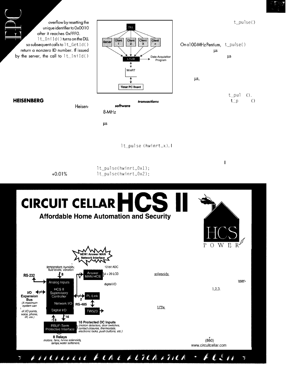
keeps the DLL resident as long as the server
is resident, ensuring that each client re-
ceives a separate unique identifier.
1
Driver
For the client side, the C code is shown
in Listing 3a. Listing 3b shows the code for
the server.
INTERFERES
it
takes time to measure time. The
berg principle applies when timing soft-
ware transactions just as it does in other
settings.
Figure 2-Here are the interactions among
components far timing
in a cli-
ent-server
system.
the
crystal providing the time base
for the counter. It can cause inaccuracies of
10
for each minute the timer is run.
How much does the timing hardware
and software interfere with the process it’s
trying to time? The board’s design guaran-
tees that software doesn’t interfere with the
registration of events reaching the input
lines. Thus, for external events, the timer
softwaredoesn’taffectthetiming precision.
For software timing, some amount of
interference is unavoidable. First, it takes a
finite amount of time to write to the timer
boardusing
evaluated this time by delivering two suc-
cessive pulses using the code:
This board’s only limitation for timing
external events is the
precision of
Thedurationofonecall to 1
can be estimated by computing the differ-
ence between the times registered as a
consequence of these two function calls.
1
takes
an average of 45
under Windows 95
(range 43-l 19) and 88
under Win-
dows NT (range 86-448).
For 1250 samples under Windows NT,
1246 of the durations were between 86
and 90
and 4 were much longer. The
long-duration intervals represent instances
when the application’s timeslice ended
between the two calls to 1
se
The delay introduced by 1
u 1 s e
can be reduced to one bus I/O cycle by
redesigning the output logic on the board
to be driven from a memory-mapped loca-
tion rather than an I/O port. Or, the same
result can be achieved by driving the timer
board’s inputs with a digital output board
already designed this way.
Second, the data-acquisition program
takes finite time and makes all software
functions appear to take longer, on aver-
age, than they
really
do.
used thesoftware
timing strategy outlined in this article to
measure how long it takes to drain 100
Our concept of building a home control system is based on the principles
embodied in building an original Heathkit. Besides giving you a project which
details everything from the theory of operation to instructions for fabricating a
functioning system, we give you the sense of confidence that comes from success.
Light level, voltage
to PC
and DAC
keypad scanner,
bidirectional
have hundreds
X-l 0 AC Power
Line Control
(AC
actuators,
garage doors, door locks, HVAC, etc.)
The HCS II is designed with an economical central core and an expand-
able network. A basic system consists of the HCS II central processor,
which incorporates direct analog and digital I/O with real-time event
triggering; a PL-Link wireless X- 10 AC power-line interface which
has sixteen contact-closure/voltage inputs and eight 3-A AC/DC relay
outputs for
motors, lamps, alarm horns, and so forth.
The house event control sequence is written on a PC in a unique,
friendly control language called XPRESS and stored on the HCS in
nonvolatile memory. Building them is as easy as
Of course, we have lots of extra stuff like our new Answer MAN network
module when you want to expand the basic system. The full HCS has
phone and modem interfaces, infrared remote control, voice
synthesizers,
and much more.
A Circuit Cellar HCS II is not for passive people and definitely not for the
masses. It is for a special technical breed that wants a challenge with
a tangible reward. Discover the world of manageable and affordable
home automation and security.
Circuit Cellar. Inc.
Park St., Vernon, CT 06066
8 7 5 2 7 5 1
l
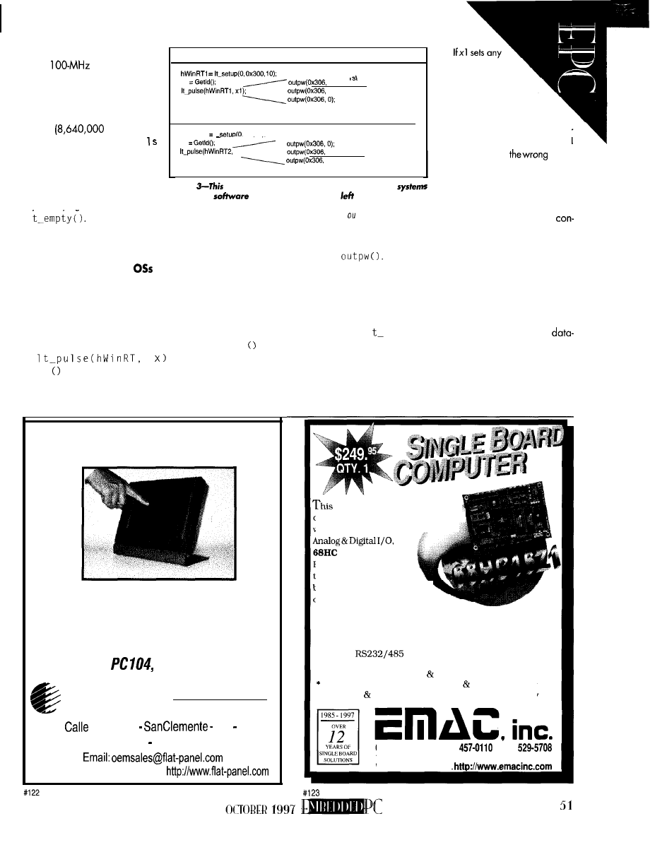
events from the timer board’s FIFO
on my
Pentium.
It takes an average of 7.4 ms
under Windows 95 and 16.2 ms
Client1
Driver
Real Time
bits that were al-
,
xl
0);
ready set by x2, then
xl);
End of Timeslice
the outcome is incorrect.
3rd
under Windows NT 4.0. Thus, if
Because the input lines on the
the mean rate of events is 100 per
Client2
Driver
Real Time
timer board are triggered by
second
per day) and
positive edges rather than by lev-
the thread is sleeping for
hWinRT2 It
0x300.10):
x2
els, the event signaled by xl will
between event retrievals, then this
x2);
x2);
2nd
0);
End of Timeslice
4th
be registered with
mask.
thread uses less than 1.6% of the
The bad luckoccurs, albeitwith
total time availableon thesystem.
These times can be improved
Figure
figure shows how multiprocessing operating
verylowprobability, becausedata
by modifying the source code for
can cause
race conditions. From
to right, the three
written to theoutput port is latched
columns show the sequence of software timing calls from the point
by the output drivers. Software
1
All these timing
of view of two concurrently running clients, the tpw calls from the
software libraries, and the difficulties that result in real time.
creates pulses through three
numberswould be proportionately
secutive writes to the oufput port.
faster on faster processors.
MULTIPROCESSING
The software timing applications out-
lined here are designed to create the least
possible interference with the transactions
they’re trying to time. To do this, I’ve
adopted a slightly quick-and-dirty method
to write pulses to the board.
c a l l s
out pw
three times in rapid succession to
write 0, x, and 0. This setup provides the
software equivalent of race conditions if one
client’s timeslice ends and another’s starts
during the sequence of calls to
Figure 3 outlines the critical situation.
Suppose that clients 1 and 2 are both
active and that they’ve acquired different
identification numbers [e.g., xl and x2).
Also suppose the timeslices dictated by
the OS contrive to interrupt client 1 in 1
pu
1 se
before xl is written to the output
port and then interrupts client 2 and rein-
states client 1 after x2 is written. The driver
handles this fine, but the sequence of writes
to the output port is 0, 0, x2, xl, 0, 0.
Touch The Future
LCD Touch Monitors
L C D T o u c h S c r e e n s
V G A L C D D i s p l a y s
LCD Controllers
ISA,
Analog, Video
E A R T H
Lowest Prices on Earth!
Computer Technologies
1110
Cordillera
CA 92673
Ph: 714-361-2333 Fax: 714-361-2121
FREE CATALOG available at
The buffer circuit in Figure 4 can be put
between the output and input connectors of
the timer board to convert a single write to the
output port into pulses on the active lines.
This circuit takes advantage of a brief
data available pulse (DAV) placed on one
pin of the output connector each time any-
thing is written to the output port. The
ready pulse is delivered even if writing to
the output port doesn’t change the voltage
on any of the output lines.
Writing x2 and xl (or even xl and xl)
sequentiallycausespulsestoappearon the
board comes ready for
Iemanding
applications,
vith
16
bit DSP capability,
and
11 Compatibility.
3ackdoor Debug and up
o one Megabyte of battery
lacked RAM creates a robust
.
Ievelopment environment.
* 16 Programmable I/O lines
* 8 High Drive Digital Outputs
* 8 Channels of Fast 10 bit A/D
* Optional 8 Channel, 8 bit D/A
* Up to 2
Serial Ports
* Backlit capable LCD Interface
* Optional 16 Key, Keypad Interface
16 bit Timer/Counters with PWM Clock/Calendar
* 64K RAM EEPROM included plus Flash Capability
618-529-4525 Fax
BBS
11 EMAC WAY, CARBONDALE, IL 62901
WORLD WIDE WEB:
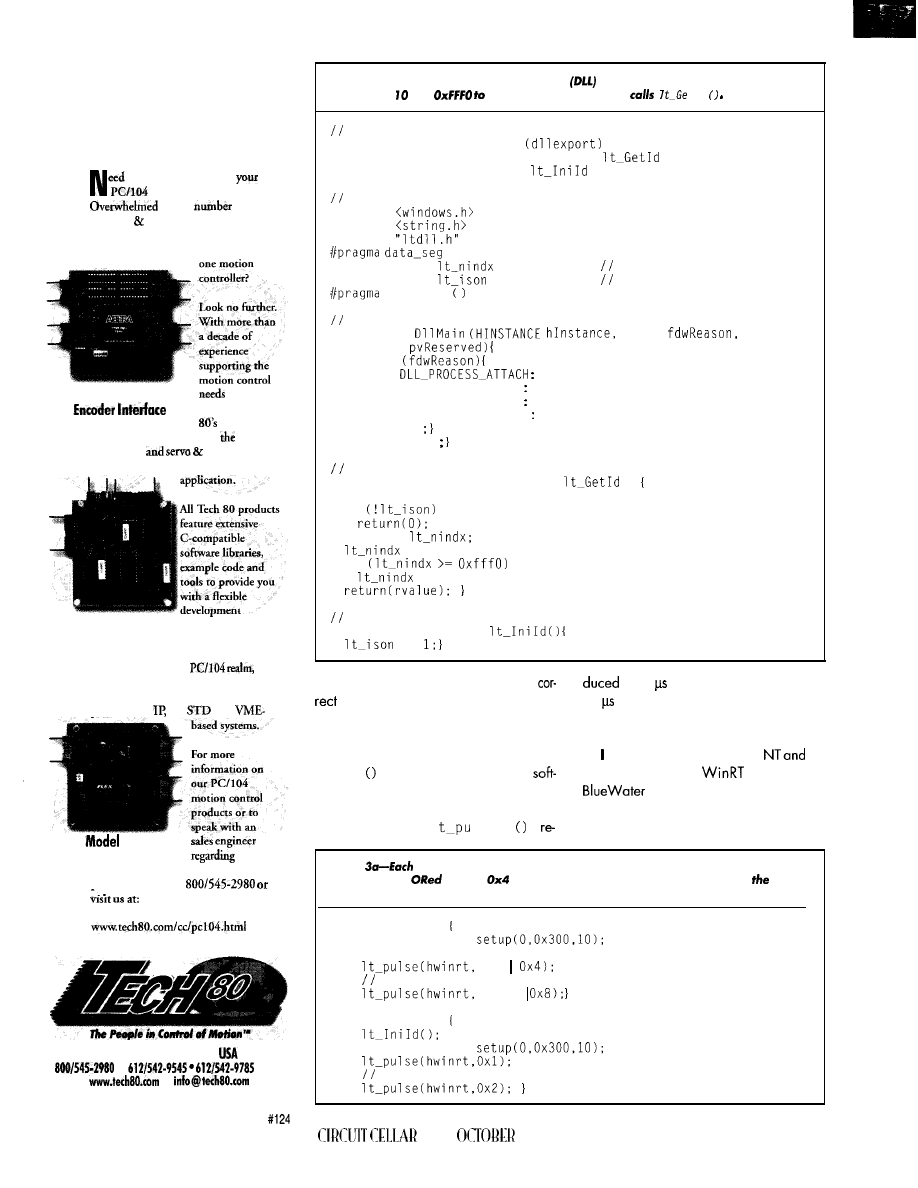
The PC/l 04
Motion Control
Experts
motion control within
application?
by the
of
products vendors out there? Looking
for a motion control specialist instead
of just another PC1104 vendor with
Model 5912
of OEM
customers,
Tech
family of
DC1104 modules can meet
encoder
interfacing
stepper control
demands of your embedded
Model 5928
environment.
Servo Controller
AND if your needs
extend beyond the
Tech
80 has the industry’s most extensive
line of board-level motion control
products for PC,
and
5936
Stepper Controller
your
current project,
please contact us at
Minneapolis, Minnesota
l
(fax)
l
52
listing 2-This complete dynamic link library
assigns a unique identification number
between Ox and
each software client that
t I d
LTDLL.H header file
#define EXPORT _declspec
extern EXPORT unsigned short CALLBACK
(VOID);
extern EXPORT void CALLBACK
(VOID);
LTDLL.C
#include
#include
#include
("shared")
unsigned short
= 0x10;
unsigned short
= 0:
data_seg
next index to assign
is the DLL activated?
Generic DLL main routine-does nothing
int WINAPI
DWORD
PVOID
switch
case
case DLL-THREAD-ATTACH
case DLL-THREAD-DETACH
case DLL-PROCESS-DETACH
break
return TRUE
Assign a unique ID number
EXPORT unsigned short CALLBACK
0
unsigned short rvalue;
if
rvalue =
+= 0x10;
if
= 0x010:
Reset ID numbers
EXPORT void CALLBACK
=
correct output
lines
for both writes. The
to 22
under Windows 95 and to
input lines are pulsed, and the correct
76
under NT.
masks are recorded by the timer board.
If the buffer circuit is used, there’s no
DRIVER IMPLEMENTATION
need to create pulses with three calls to
implemented the Windows
95
out
pw
A single call suffices, the
drivers using the
toolkit from
ware race condition never occurs, and (as
Systems. It’s extremely easy to
a pleasant side effect) the amount of time
use and the exact same API is presented for
taken by the sleeker
1
1
se
is
both operating systems.
listing
client program obtains a unique
ID
and issues start and end pulses that
a r e t h e I D
w i t h
or 0x8. b-The server turns on
ID issuer
and generates start
and end pulses for each transaction on lines Ox I and 0x2.
a)
client_mainO
HANDLE hwinrt =
unsigned short id = lt_GetIdO:
id
client code goes here
i d
b)
server_mainO
HANDLE hwinrt =
server code goes here
INK
1997
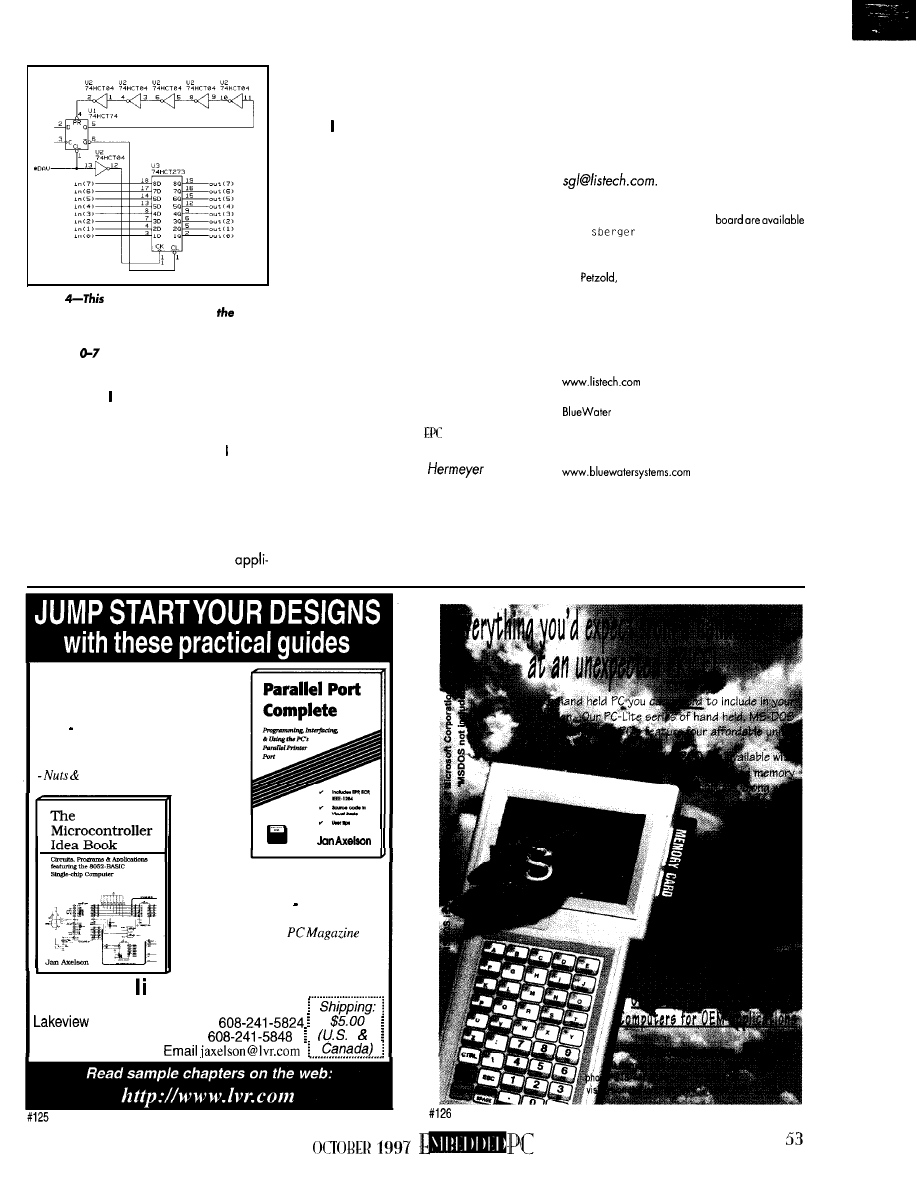
Figure
buffer circuit can be inserted
between the output and input to
timer
board to convert its latched high or low
outputs into pulses on each line that is high.
Only bits
are shown.
Without knowing much about either
Windows OS,
was able to port my DOS
library to a workable NT and 95 system in
about
10 hours. The library developed on
Windows 95 worked the first time tried it
in NT. The toolkit is relatively inexpensive,
and if you want to expand on the capabili-
ties of my API, you can do so easily.
The WinRT toolkit isn’t intended for high
rates of data acquisition because its generic
driver interprets commands from the
cation program. Thus, the relatively long
times needed to retrieve 100 events from
the timer board can be attributed to the
driver used rather than to any slowness
caused by the timer hardware.
It’s possible to improve substantially on
the time needed to retrieve 100 events by
making a specialized driver using a DDK.
PROJECT WRAPUP
The timer board provides microsecond
precision in timing the intervals between
external events. But, with minor software
and hardware modifications, it also times
software transactions.
My methods are an excellent compro-
mise between the ideal (no Heisenberg)
and the real, asynchronous world of mod-
ern computing. Near perfection can be
attained through feasible improvements I
mentioned in the text.
Special thanks to Dave
for assis-
tance in designing and manufacturing the
timing board, Paul Lever of Blue Water
Systems for hints on timing software trans-
actions, and Adam Bernstein and Paul
Lever for their helpful comments.
Steve Lisberger is a neuroscientist at the
University of California,
San
Francisco. He
also owns lisberger Technologies, a small
business dedicated to innovative
solutions
for the problems of
real-time data acquisi-
tion and analysis. You may reach Steve at
SOFTWARE RELEASE
Completeschematicsforthetiming
in
1 i
.pdf andmaybedownloadedfromthe
Circuit Cellar Web site.
REFERENCES
C.
Programming Windows 95, Microsoft
Press, Redmond, WA, 1996.
SOURCES
Timer-board hardware and libraries
Lisberger Technologies
848 Clayton St.
San Francisco, CA 941 17
(415) 661.2097
WinRT toolkit
Systems, Inc.
P.O. Box 776
Edmonds, WA 98020
(425) 771.3601
Fax: (425) 771-2742
I R S
416
Very Useful
417 Moderately Useful
418 Not Useful
NEW!
“A focused book that
delivers what it promises: detailed
technical information on the parallel
port.” Windows Developer’s Journal
“It’s been a while since I’ve seen a
book as practical as this one.”
Volts
ISBN 0-9650819-l-5
$39.95
343 pages
Includes disk
MICROCONTROLLERS!
“An ideal introduction to low-end
embedded design.” EDN
“The writing is a model of clarity
and conciseness.“-
ISBN O-96.50819-0-7
273 pages. $31.95
Order ne: I-800-247-6553
For more information or international orders:
Research Phone
2209 Winnebago St. Fax
Madison, WI
53704
Steps old
There are
times
when
feenie-weenie
04
factor just doesn’t cut if.
Why? Because if fakes
7-2 years
for
latest desktop
shrink enough
and sometimes you need more high-end functions on a board.
EBX.
ith all the hype over Pentium Pro,
and sizes. Back when all embedded
Java, and the Internet, an article
have become the norm, today’s designers
puters were based on proprietary designs
on a new single-board computer form-factor
are using off-the-shelf embedded computer
using a microprocessor or single-chip
standard might seem mundane. After all,
modules wherever possible. This way, they
microcontroller, you simply designed your
a
few hundred engineers
design
can put more attention on software,
electronics to fit the requirement.
But, if you’re one of the few who specify or
aging, and specialty interfaces.
But as
MHz
DRAM over
design embedded systems, read on.
But when it comes to off-the-shelf
64 MB, high-resolution graphics,
If
your specs call for a high-performance,
one size can’t possibly fit all applications.
networking, and highcapacity
data
storage
That’s why there are so many form factors.
highly functional embedded
computer that fits within a
physicallychallenged environ-
ment, the new EBX standard
may be what you need.
And, it isn’t just size.
There’s also the physical
arrangement of boards to
think about. Early
shelf embedded computer
solutions were based on a
variety
of backplane buses
(e.g., STD, Multibus, VME,
and G64). Even the PC/AT
architecture was adapted
to a backplane bus (i.e.,
the passive-backplane PC).
A N O T H E R S T A N D A R D ?
No doubt you’re wonder-
ing, “Don’t we have enough
standards?” After all, there’s
STD, Multibus, VME bus,
G 6 4 , p a s s i v e - b a c k p l a n e
PC, PC/ 104, PC/
and probably
a few we’ve forgotten to list.
But remember, embedded
systems come in all shapes
56
Figure
familiar? The new EBX standard evolved from
venerable
Little Board form factor.
These multiple-board so-
lutions require a “passive”
backplane with several
boards plugged in perpen-
dicularly, supported by a
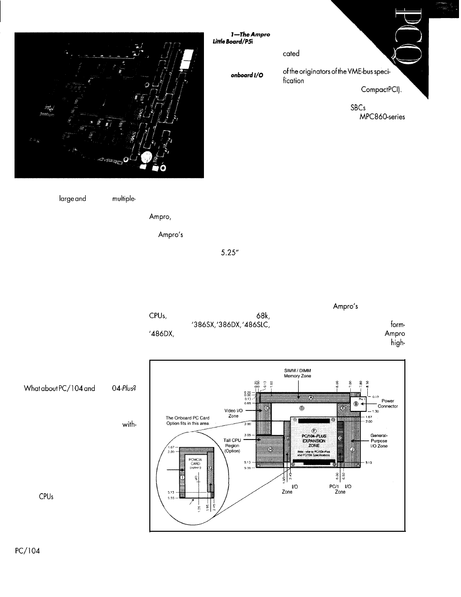
metal card cage to hold it all in place. The
result is a rather
complex
board configuration, which often cannot fit
That’s not to say that backplane buses
within the space-constrained environments
aren’t great for lots of nondesktop applica-
tions, especially when system specs call for
of embedded applications.
half a dozen or more easily swappable
function modules (e.g., rack-mounted indus-
trial-control computers and telecommuni-
cations switching systems).
But, backplane configurations usually
can’t fit the kind of applications where
embedded microcontrollers were tradition-
ally used. They just don’t fit the size and
other mechanical constraints of applica-
tions like portable test equipment, medical
diagnostic instruments, operator interface
displays, mobile control and monitoring
systems, and many other embedded con-
trol applications that come to mind.
PC/l
After
all,
these popular embedded-PC build-
ing-block standards were designed to fill the
need for a modular off-the-shelf approach
to deeply embedded system design,
out
the
mechanical limitationsof backplanes
and card cages.
Sure, PC/l 04 modules help you avoid
reinventing the wheel for embedded PC
systems. But, even PC/ 104 isn’t a perfect fit
for every application.
Why? For one thing, when the latest
desktop
are first introduced,
they don’t
come in small enough packages to reliably
fit on PC/l 04 CPU modules. It usually
takes l-2 years for them to shrink enough
to fit the compact PC/l 04 form factor.
Another problem is that the compact
form factor naturally limits how
Photo
takes
advantage of the EBX
tall CPU option to of-
fer an Intel Pentium
processor along with
lots of
in
the EBX-compliant
SBC.
many high-end PC functions you can fit on
a single module along with all the required
I/O connectors. These are the reasons why
Little Board has been around
for over 14 years. Originally patterned
after the footprint of the
disk drive,
the inventor of PC/l 04, continues
this form factor has been used in thousands
to support its little Board SBC form factor.
of applications and continues to be quite
popular for new designs.
Over the years, this form factor has been
used by dozens of embedded computer
suppliers and has hosted lots of different
including the 280, 64180,
80186, ‘286,
Pentium, and now Motorola’s
PowerPC-which brings us to EBX.
MOT’S MOTIVATION
Motorola has long advo-
open architectures and
industry standards. They were one
and continue to support new and
emerging standards (e.g.,
In August 1996, Motorola started work
on a new MBX family of
based on the
Motorola MPC82 1- and
PowerPC microprocessors, which are highly
integrated devices with an on-chip integer
and communications processor.
A key design goal of MBX was to be
physically smaller than conventional PC
motherboards, yet offer higher price/per-
formance and functionality. It had to be
small enough for deeply embedded appli-
cations but large enough to contain all the
embeddedcomputerfunctionalityrequired
for a specific task or application.
Motorola was already manufacturing
desktop PC/AT-style motherboards based
on the PowerPC processor in the ATX desk-
top motherboard form factor. But embedded
applications need something smaller and
more rugged.
It quickly became apparent that no
industry standard met Motorola’s needs.
The closest match was the form factor
implemented on
Little Board and
by several other SBC companies.
At about the same time Motorola’s
factor search was taking place,
was getting ready to announce a new
PC1104
04
end SBC-the Pentium-
based Little
with
PC/l 04.
Unbeknownst to Motorola,
the Little
was about to
PCI to PC/l 04 and, hence, to the
Little Board form factor. PCI on the Little
Board form factor made it even more inter-
esting to Motorola, since PCI was to be a
key feature of the MBX product family.
The companies agreed to convert the
Little Board form factor into an
open, multivendor, and architecturally neu-
tral standard-the EBX (embedded board,
expandable) form-factor specification de-
picted in Figure 1.
THE END PRODUCT
The EBX form factor is small enough for
deeply embedded applications, yet large
enough to offer the functions of a full
embedded computer system-CPU,
memory, mass storage interfaces, display
controller, network interface, serial/parallel
ports, and other system functions.
EBX isarchitecturallyneutral, so itdoesn’t
specify that the architecture must be PC
even that the CPU be ‘x86
your
for the most, high-
powered,
set of
and hardware development tools for
embedded
development.
1: Paradigm LOCATE the most popular tool for
creating embedded C/C++
Borland and Microsoft
2: Paradigm
DEBUG the only x86 debugger
RTOS,
language, and
emulator
support; 3: Paradigm SUPPORT the best
s u p p o r t the
supplied to
customers for
Developing real-time embedded applications doesn’t have to be
time consuming or difficult-you just need to have the right
Paradigm alone has the high performance development tools you
need to streamline the embedded system software development
process so your Intel and AMD
applications are ready in record
time. Paradigm’s complete suite of tools work with industry standard
C/C++ compilers from Borland and Microsoft, as well as hardware
development
from Applied Microsystems, Beacon Development
Tools and other popular in-circuit emulator vendors.
country
2214
NY
l-800-537-5043
Call us at 800-537-5043 today and let take care of all your
development tool needs. so you can keep your focus where
you need it-on your application.
compatible. As a result, the first two
compliant products, the Pentium-based Little
from
(Photo 1) and
Motorola’s PowerPC-based MBX SBC
(Photo
are different architecturally.
EBX SPEC
As you see in Figure 2, the key features
of EBX are its:
l
rectangular (5.75” x 8.00”) form factor
l
PC/l
expansion stack location
l
eight mounting-hole pattern
l
seven-pin power connector
l
recommended areas for l/O connec-
tions, DRAM, CPU, and optional PC
Card slots
The EBX
provides two drawings
that define regions for various types of I/O,
SIMM or
memory, and one of two
basic configurations (i.e., the tall-CPU and
PC Card-slot options).
The tall-CPU option is intended for
(e.g., Intel’s Pentium), which
require heat-sink assemblies. The PC
slot option specifies a recommended loca-
tion for
PC Card slots (see Figure
assuming a smaller, lower profile CPU
can fit in the PC/l
expansion loca-
tion beneath any plugged-in modules.
The
expansion stack is
one of the most important aspects of EBX.
PC/l
basically implements the same
electrical bus as desktop ISA and PCI but in
the form of rugged and reliable
socket connectors instead of the desktop
motherboard’s edge-card connectors. This
setup results in a modular, compact, and
highly rugged assembly.
With approximately
in? of real es-
tate,
have enough
space to implement a high level of perfor-
mance and functionality on a single card.
Still, it fits within tight space budgets.
modular expandability lets you
easily adapt an EBX SBC to match the
needs of your project. Further flexibility
comes from the
PCMCIA sockets
(or a plug-in PC/l O&based PCMCIA inter-
face with the tall-CPU option), which offer
access to PC Cards from the mobile and
hand-held computing markets.
USING EBX
The dimensions of EBX (5.75” x 8.00”)
are about the same as those of many
resolution LCD panels. EBX
are
58
CIRCUITCELLAR INK OCTOBER 1997
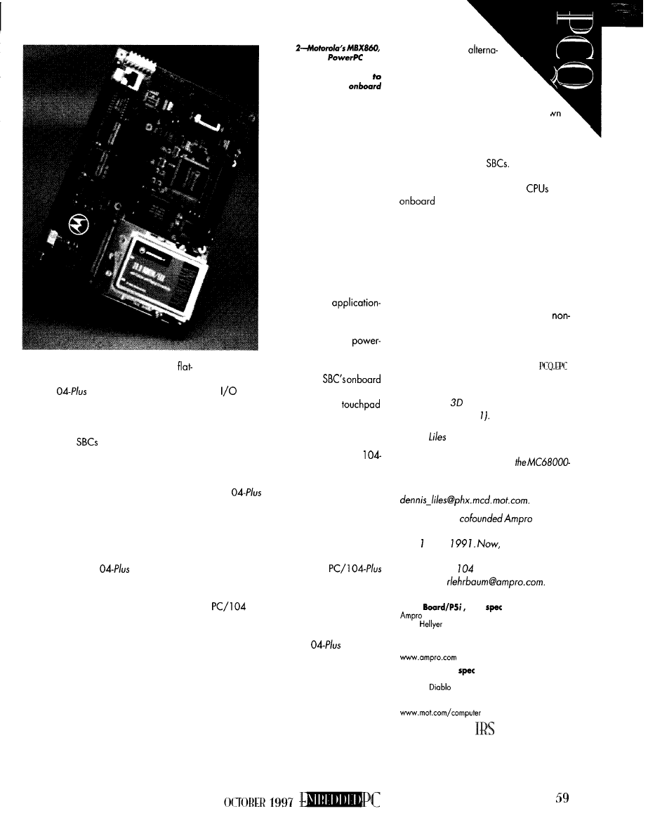
fore well-suited as the brains behind
panel operator interfaces. With its modu-
lar PC/l
expansion, EBX makes a
great basis for a panel-PC SBC.
A common question is, “On average,
how many PC/l 04 modules are plugged
into the EBX
in typical embedded
applications?” The answer: one.
Due to the uniqueness of most embed-
ded systems, such applications require at
least some custom electronics. Often, sys-
tem designers create a custom application
board that contains all required functions
and interfaces not provided directly on the
EBX SBC.
This board plugs into the header con-
nectors of the PC/l
bus, resulting in
a two-board sandwich consisting of the
EBX SBC and the application board. De
pending on bandwidth and other require-
ments, the application board may interface
to the EBX SBC using signals of the ISA bus
only, the PCI bus only, or both.
As for size, the application board can
be PC/l 04 or EBX form factor, but it really
doesn’t need to conform to any particular
form-factor standard. Generally, the appli-
cation board takes on whatever shape
works best for the application.
Functions included on typical applica-
tion boards include:
l
specialized analog and digital I/O
Photo
based on the
800
series microprocessors, is the
first EBX-compliant SBC
implement the EBX
PC Card-slot option.
l
sensor or actuator inter-
faces
l
interfaces to
specific buses (e.g.,
CAN, Profibus, etc.)
l
power supplies or
conditioning circuits
l
filtering, signal conditioning, or connec-
tor adaptation for the EBX
l
custom keypad, display, or
interfaces
Another point to consider is that the EBX
standard includes an option for the PC/
Plus bus to be built with stackthrough con-
nectors, as on a normal (self-stacking)
PC/l
form-factor module. This op
tion lets you plug an EBX SBC onto an
application baseboard, instead oftheother
way around.
By the way, it’s interesting to note that
with stackthrough bus connectors, an EBX
SBC is a lot like a giant
module! You can, for example, unplug a
stackthrough-bus EBX SBC and plug in a
form-factor SBC in its place. In
other words, either a stackthrough-bus EBX
SBC or a PC/l 04 form-factor SBC can
plug into the same PC/l
socket.
EBX FUTURE
The EBX specification has been struc-
tured in a manner that gives board design-
ers maximum flexibility and creativity and
yet stays within the confines of a standard
board specification. With backing from
Amproand Motorola, the specification will
remain architecturally neutral, open, and
royalty free.
It
provides an
tive to backplane-based so-
lutions for high-performance,
high-integration embedded corn-
puter applications and can thereby
save you from having to create your own
proprietary solution.
Already, hundreds of off-the-shelf
PC/l 04 form-factor expansion modules
can be used with EBX
And of course,
you can expect dozens of EBX SBC suppli-
ers to offer a broad range of
and
functions.
Several chassis and enclosure makers are
introducing EBX-compatible packaging
products to simplify the design of EBX-based
systems. Best of all, the EBX standard is open
tocontinued technology advancements, since
it is processor and payload independent.
One last comment: EBX isn’t the first time
Intel and Motorola processors have shared
a common form-factor standard for
desktop applications. Another important
s t a n d a r d - V M E b u s - t u r n e d i n t o a
decades-long $1 B+ industry. So, keep an
eye on the emerging EBX market!
Special thanks to Daniel lehrbaum for
creating the
co/or rendering of the EBX
form factor (Figure
Dennis
is a seniorproductmarketer for
Motorola Computer Group. His primary
responsibilities are managing
based VME
module and embedded mother-
board product lines. You may reach him at
Rick lehrbaum
Comput-
ers where he served as VP of engineering
from 983 to
in addition to his
duties as VP of strategic development, Rick
chairs the PC/
Consortium. He may be
reached at
SOURCES
Little
EBX
Computers, Inc.
4757
Ave.
Son Jose, CA 95 138
(408) 360.0200
Fax: (408) 360.0220
MBX SBC, EBX
Motorola Computer Group
2900 S.
Way
Tempe, AZ 85282
(512) 434.1526
4
19
Very
Useful
420
Moderately Useful
42
1
Not
Useful
anagfng a
Fred offer a
traditional data-collection technique? No way. Instead, he’s taking
the hardware he selected last month, starting at the sensor end, tracing the
datastream to the
flash
I
e,
and serving it to a
Web browser.
ast time, described the hardware
we’ll use to collect our plant-growth cham-
ber (PGC) data (INK 86). So, right now,
you’re expecting another run-of-themill
collection article like the hundreds you’ve
read in other magazines.
Not from me, buddy! I’m going to start
at the sensor, follow the serial datastream
to the SBC 301 flash file, and then “serve”
it out to a waiting Web-browser screen.
Yep, you read it right: “serve”
You
know what that means, so let’s light the
fuses on those solid boosters and put our
PGC in orbit.
UP THE DATA
If you recall, the
was speci-
fied as the sensor interface because its
characteristics are well-suited for the PGC
data-gathering application. The physical
interfaces are shown in Figure 1.
Under the covers, the PIC will fire off
A/D conversions that import data from the
humidity, temperature, and carbon-diox-
ide sensor array. Once the sensor data is
60
realized, the PIC is responsible for convert-
ing the floating-point data into a numeric
format that can be stored in the embedded
platform’s flash.
A
simple serial connection
is the conduit to transfer the converted
sensor data from the
internals
to the SBC 301’s flash disk.
I won’t go into the inner workings of the
PIC 14000. That’s an article in itself. Matter
of fact, I’ve already covered it (“Take Your
PIC-A took at the PIC
65). Meanwhile, Figure 2 represents the
programmatical flow taking place within
the
firmware.
MEASURING PGC TEMPERATURE
The temperature is taken by measuring
the voltage across a voltage-divider network
and calculating the resistance of the plati-
num RTD. To reduce RTD self-heating and
improve measurement accuracy, the cur-
rent through the RTD should be in the
vicinity of 0.5
Ideally, at
our voltage divider
should have a total value of 10
Under
INK
1997
ideal conditions, this should produce a
Basic Ohm’s law says that if the RTD
changes resistance, which it will as its
surrounding temperature fluctuates, the to
tal voltage divider resistance will change
and affect the current flowing through the
resistors and RTD.
Since the PIC is not really measuring
resistance, I have to derive the RTD resis-
tance using a voltage measured across a
known resistance in the divider. Once the
voltage across the known resistor is taken,
I can then calculate the current flowing
through the voltage divider as a whole.
At that point, have a known current
value that enables me to calculate the new
total resistance value of the voltage di-
vider. Since two of the resistances are
constants, it’s then a simple matter of
grade arithmetic to resolve the RTD resis-
tance.
The RTD resistance is plugged into the
resistance-to-temperature function and a
resultant temperature is derived:
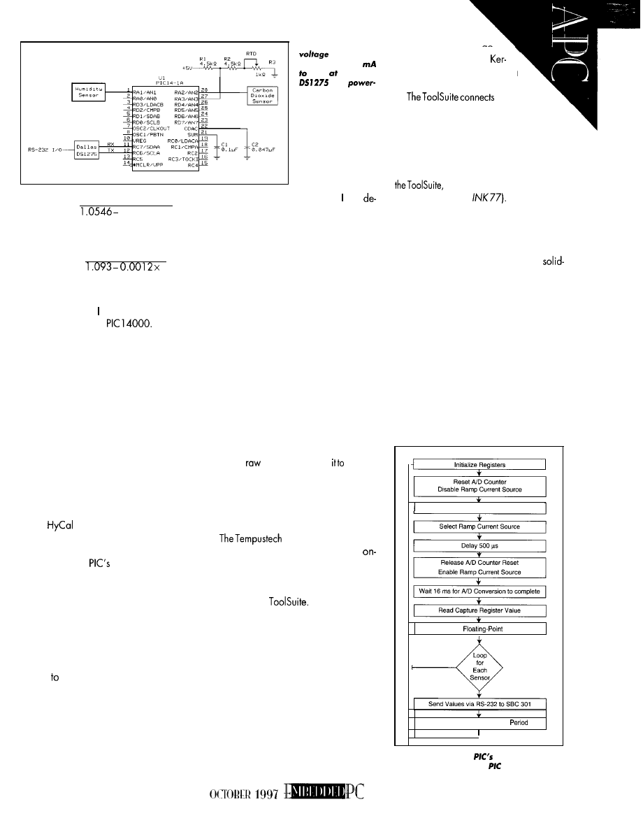
Figure I-Ideally, the
divider al-
lows exactly 0.5
flow
0°C. The
is an
stingy I-pin RS-232
interface IC.
True RH =
Sensor RH
and temperature measurements, can
0.002 16x T
rive the true relative humidity.
for Tin degrees Celsius, or
True RH =
Sensor RH
T
for Tin degrees Fahrenheit.
Another plus to measuring the higher
voltage point is that don’t have to preload
the A/D input of the
If I mea-
sured across the RTD itself, the input volt-
age would be too close to the minimum
voltage that the PIC A/D input circuitry
needs to take a meaningful reading.
What I mean by preload is to program
the PIC input to add about 0.45 V of offset
to the input voltage. Thus instead of mea-
suring 0.5 V, the inputactuallysees0.95 V.
Of course, the offset is compensated for in
the PIC measurement software.
MEASURING PGC HUMIDITY
Humidity is a bit simpler to measure
than temperature. The work has already
been done.
The
humidity sensor is equipped
with integrated signal conditioning. I sim-
ply attach the output of the humidity sensor
to another of the
A/D input pins and
read the sensor’s output voltage.
My selected humidity sensor is capable
of supplying a voltage that varies from
0.8 Vat 0% RH to 3.9 V at 100% RH. The
particular sensor used in this application
provides 0.807 V at 0% RH and 3.015 V
at 75.3% RH. Assuming a linear output, I
easily convert the humidity sensor’s output
voltage
a
relative-humidity measurement.
All is not done when the voltage is
measured, though. Remember that relative
humidity is temperature dependent. So, I
have to add a little math to the mix.
I always know the temperature because
I’m tracking it. So, using the formulas
above along with the mechanical humidity
PGC CO, LEVELS
Using the UIP program that complements
the Telaire 200 1 V, I arbitrarily set the maxi-
mum detectable carbon-dioxide level to
2000 ppm. Measuring the CO, levels is
akin to measuring relative humidity. Again,
most of the work is already done for me.
The
Telaire
can output a O-l O-V analog
voltage that’s proportional to the minimum
and maximum ppm value set with the UIP
program. Just as with the humidity sensor,
the output is linear and the carbon dioxide
levels are interpreted according to sensor
output voltage.
DEPARTING SENSOR SPACE
So far, I’ve defined the sensor-scanning
process. The PIC 14000 will use its talents to
assimilate
data
and convert
numeri-
cal format. Using a software-based serial
interface, the data can be transmitted to the
SBC 301 for storage and later processing.
DATA-COLLECTION SECTOR
SBC 301 is ideal for
this
application. With only 2 MB of flash
board, we have to be
skimpy with
the code.
DOS would be overkill here, so let’s
embed our own kernel using Phar tap’s
TNT Embedded
The advantages
to this are many.
First of all, the ETS is designed espe-
cially for embedded-system use. The ETS
Kernel alone provides a simple operating
system for running this PGC application.
Another plus is that the ETS product uses
industry-standard compilation and debug
tools. The program that will effect the PGC
sensor scan and storage routines is com-
posed of standard Microsoft C code.
All the set-up and initialization routines
are part of the standard ETS Kernel, so I
don’t have to code that stuff. The most
important reason to go
this way is that the ETS
nel is relatively small, weighing
in at around 25 KB.
a host PC to
theembedded targetvia parallel or serial
interfaces. Once connected, the software is
developed on the host and transferred to the
target embedded platform for execution.
You can clearly see the advantages.
Again, I could write a whole article just on
but I did that, too (“Embedded
PC Development,”
So, let’s move
on and describe what the code will do.
Basically, the SBC 301 need only poll
the PIC 14000 at a predetermined interval
and retrieve the numerical data into its
solid-state disk. Software to effect the
state disk is included with the SBC 301
embedded PC. It’s easy to implement and
has a variety of configuration possibilities.
Since the PGC configuration won’t be
transmitting the data to any point in real
time, I chose to configure the solid-state
disk as drive C. This setup enables the SBC
301 to start the ETS Kernel in processor
stand-alone mode.
When the collected data needs process-
ing, a real-live drive D will be added that
contains its own ETS-based program to
process and serve the collected data.
Select Input Channel
Convert
Value
Wait for Next Measurement
Figure 2-Here’s a
eye view of the
firmware running in the
14000.
61
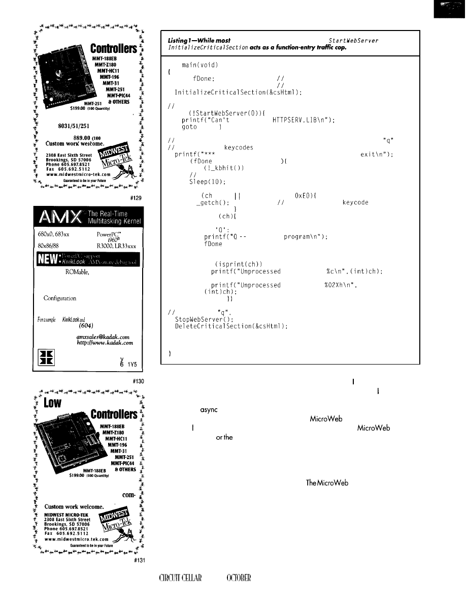
80251 Embedded
Midwest Micro-Tek is proud to offer
its newest line of controllers based
on the
architecture.
The 8031 comes in at a surprisingly
low cost of
quantity).
MIDWEST MICRO-TEK
80386 protected mode
family
real mode
family
l
Compact,
fast interrupt response
l
Preemptive, priority based task scheduler
l
Mailbox, semaphore, resource, event, list,
buffer and memory managers
l
Builder utility
l
Comprehensive documentation
l
No royalties, source code included
of
description
of AMX,
Phone:
734.2796
F a x : ( 6 0 4 ) 7 3 4 - 8 1 1 4
E-mail:
W e b :
KADAK Products Ltd.
206 1847
West Broadwa
Vancouver,
BC,
Canada
V J
Cost Embedded
If you’re interested in getting the
most out of your project, put the
most into it. Call or Fax us for
plete data sheets and CPU options.
of the work is done by the
function,
int
BOOL
flags program ready to terminate
char ch;
character typed by user
Start Web server
if
initialize
ERR:
Loop reading and processing keystrokes until user types
Since Z-byte
are not currently used, they are discarded
Waiting for HTTP requests, type 'q' to
for
= FALSE: !fDone;
while
yield rest of time slice
ch = _getchO;
if
== 0 ch == (char)
discard Z-byte
continue:
switch
case 'q':
case
quitting
= TRUE:
break;
default:
if
keystroke:
else
keystroke:
break:
User typed
Tell Web server to terminate.
return 0;
ERR:
return 1;
W E B T R A N S P O R T R E A D Y
You didn’t really think I’d use all that
computing power within the SBC
301
just
to do simple
communications and
data logging, did you?
W h e n spoke of “serving,” I wasn’t
talking Wimbledon
U.S. Open. I was
talking Internet and Intranet.
Just so happens that the Phar Lap TNT
package I have is the latest and greatest
they’ve got. It includes services that enable
the implementation of a full-blown Web
server-embedded, of course.
The idea is to collect the data from the
PIC and place it in nonvolatile solid-state
disk. Once the PGC package is retrieved,
add a D drive that contains the embedded
Web server and present the collected data
in any format desired via any standard
GUI-based Web browser.
All of a sudden, don’t have to write any
host data-display code and can make the
data display really fancy
with
minimal effort.
I like that. Here’s how the Phar Lap embed-
ded
Server works.
The Phar Lap ETS
Server is a
collection of libraries and plug-insdesigned
specifically for embedded systems that are
linked with a user-written application to
create an embedded Web server running
under the control of the Realtime ETS Kernel.
Servercan generate HTML
pages on-the-fly in standard C code. Present-
ing the data is no problem. It’s just HTML!
Using server-side-generated HTML, the
designer can embed any information col-
lected from the PGC
into static HTML pages.
These on-the-fly pages can then be served
via normal communications channels to any
W eb browser for viewing.
62
INK
1997
listing
the “needs slashes” entries. This makes sure that the correct syntax is
entered regardless of the user’s little fingers.
=
(void
N U L L ,
1 o.
,
( v o i d
1 o World”
,
( v o i d
lo World with embedded
HTML" ,
“di
( v o i d
“Next level of HTML examples”,
(void
N U L L ,
“ d e b u g / “ ,
( v o i d
“ O n - l i n e d e b u g g e r ” ,
“debug”,
(void
N U L L ,
NULL
Depending on the environment, the
pages can be served via Ethernet LAN,
asynchronous point-to-point protocol, and
PPP or SLIP protocols. The desktop interface
is designed with any of the standard com-
mercial HTML editors. If you’ve ever put
together an HTML Web page, you can
design the data-display interface.
Four libraries make up the
Server. All the real work is done within the
HTTP Server Library.
This library implements an embedded
HTTP/l .O micro server compliant with the
RFC 1945 standard. User-written server
programs call functions within this library
to effect the actual network communications
that make the server go.
The user program must begin the serving
process
by
calling the
function, which creates synchronization
initializes the
interface,
and starts a thread that sleeps while wait-
ing to service incoming
requests.
The mere mention of threadsand program-
matic sleep implies that the ETS Realtime
Edition supports real-time programming. In
fact, it includes software mechanisms to
effect a deterministic scheduler and man-
age preemptive multitasking of threads.
By using real-time-programming meth-
odology, the
Server checks in
as a lightweight embedded application
with heavyweightskills. Toefficientlyservice
multiple
requests concurrently, the
server must be able to start a new thread for
each
request.
By starting a new thread for each client
request, the chances of overrunning the
socket connection queue are pretty much
eliminated. As a result, HTTP request re-
sponse times are reduced.
Just like the ETS Kernel process, the
Server contains code ensuring
that all necessary server start-up processes
actually come up and run. We don’t live in
a perfect world, and neither does the data.
Web application of any problems that may
occur during server startup. The program-
mer may embed any information deemed
necessary
within
the
code to
help the user identify the problem.
The HTTPSERV.
LIB
library is the truth
and the lightwhen
to creating
server threads.
server threads process
client requests and serve the proper HTML
data and/or error pages.
Once the start-up process is completed
without error, the designer’s main program
can simply loop waiting for userdefined
keystrokes. These keystrokes are decoded to
perform user-initiated tasks until a request
Circuit Cellar Plant Growth
Chamber Readings
Photo
not real fancy,
you
idea.
T h e
sky is the limit.
IF
YOU
YOU NEED
ELECTRONIC
EXTENDERS
PCI
PCI Mini Extender
Insert/Remove
Cards
With PC Power On!
Save Time Testing And Developing Card!
Save Wear On Your PC From Rebooting
Adjustable Overcurrent Sensing
NO Fuses, All Electronic For Reliability
Single Switch Operation W/Auto RESET
Optional Software Control Of All Feature!
Breadboard Area For Custom Circuitry
And More...
Passive MC32 Extender
Passive ISA Extender
AZ-COM. INC.
24-Hour Fax on Demand:
510-947-1000
Ext.7
63
to serve data or
nate the Web server is
in.
In the
Server
amplecode included with
Suite, a received from the keyboard
calls the
function, and
you know what happens then. Listing 1
outlines the Web-server start-up task.
The second library is concerned with
HTML pages. The functions included in the
HTMLPAGE.
HTML pages in real memory. You can also
redirect these in-memory pages to a file.
Calls to HTMLPAGE create empty HTML
pages, build error pages, and process
memory
and HTML files. One useful
feature contained within the HTMLPAGE
library is involved in locating and process-
ing
contained within page tables.
A URI (Uniform Resource Identifier) is a
product of a URL. For
the
Server,
page tables are directories of the prepro-
grammed or predefined HTML pages that
are available to the server. When a request
is presented in URL form, functions within
HTTPSERV. LIB are invoked to translate
the requested URL into a URI.
The URI is simply a DOS-compatible file
path pointing to a particular
file
or directory.
Each page-table entry consists of an HTML
file name, a pointer to the function that
produces the HTML page, and a text string
used as a hyperlink to the HTML page.
For example, if our target HTML file is
represented
World”,
our function to create the “Hello World”
HTML page is
1 o
and the HTML
page to be created is
1
o .
htm, a
simple click on the hyperlink begins the
page-table locate process.
The page-table entries are then scanned
and parsed. Once a URI match is found,
the function associated with the selected
URI kicks off creating the HTML page that
ultimately winds up on the browser screen.
Listing shows how a typical page-table
entry is formatted.
This is a very powerful concept. Custom
HTML
be
stored
and dynamically
assembled with real-time data on-the-fly.
The remaining two libraries are known
as “on the fly” libraries. Function calls are
madetoHTML.LIBandHTMLFORM.LIB
during the page-creation process. These
libraries contain all the functionality
sarytoassembleeach individual partofthe
HTML page to be served.
The results of the on-the-fly page-creation
process are no different than if you were to
hand code a page. Listing 3 is pretty sim-
plistic, but it’s a good picture of how a
typical on-the-fly HTML page is generated.
M I S S I O N R E P O R T
Where are we? We’ve started the
and the SBC 301 is polling the
PIC
for data. All that’s left is to process the
collected data and send it to a browser.
Sincethere’san Ethernet card on
support PGC configuration, use it as the
data-transport medium.
Most of the time, space projects depend
on funding. Funding depends on good
salesmanship. And, good salesmanship
relies on good presentation skills.
Photo 1 is the pretty picture containing
the PGC data. I used the page-table method
to get the Web page to this point.
S P L A S H D O W N
Yeah, I know. They land ‘em these
days.
But, my point is that the Internet and lntranets
are becoming the way the world communi-
cates. The Web browser has become the
defacto user interface standard in the Web
familiar, huh?
BOOL _cdecl
Open empty HTML document first
if
return FALSE:
Build HTML document
"Hello world HTML demo page");
Return completed HTML document
return
world, and
I
expect it will become the
preferred way to view data outside of that
world, too.
Do you know anyone who hasn’t used
a Web browser?
Do
you know anyone who
can't
a Web browser? I didn’t think so.
With the assistance of Phar Lap’s
Server and some really tricky
PGC sensor components, we have imple-
mented an embedded data-collection plat-
form that can serve its database to anyone
with a Web browser anywhere in the
world.
Fred Eady has over 20 years’. experience
as a systems engineer. He has worked with
computers and communication systems
large and small, simple and complex. His
forte is embedded-systems design
bereachedat
SOURCES
1 4 0 0 0
Microchip Technology,
Chandler, AZ 852246199
(602) 786.7200
S e r v e r , T N T
Phar
Software
60
Ave.
Cambridge, MA 02138
(617)
Fax: (617) 876-2972
BBS:
661.1009
ROM-DOS
Datalight
1881059thAve. NE
Arlington, WA 98223
(360) 435-8086
Fax: (360)
Survivor II Sensor
Engineering
9650
Ave.
El Monte, CA 9173 l-3093
(8 18)
Fax: (8
444-l 3 14
Ventostat
KELE Assoc.
2975 Brother Blvd.
Bartlett, TN 38 133
(901)
Fax: (901) 372-253 1
SBC 30 1
Tempustech
295 Airport Rd.
Naples, FL 34104
(941) 643-2424
Fax: (941) 643.4981
422 Very Useful
423 Moderately Useful
424 Not Useful
64
1997
DE
I
Cyliax
From the Bench
Silicon Update
MC68030 Workstation
The Boot PROM Monitor
Device Drivers
ast month, I
described the
ware architecture for a
workstation
used in our computer-architecture lab
at Indiana University. In this install-
ment, I want to discuss the
monitor software on this machine as
well as some issues that arise when
writing device drivers for I/O devices
that are
or attached to this
system’s ISA bus.
But, let’s start with what the moni-
tor does. 1’11 cover how it initializes all
the I/O devices and the processor to a
consistent, usable state.
Once this is done, I’ll show you how
the monitor implements a simple
command-line-based user interface.
This enables the student to download
and boot code from the network; boot
from a floppy or IDE drive; view and
change memory, I/O, and processor
registers; and debug programs.
In our typical lab configuration,
these machines have a VGA card and
monitor, floppy and IDE disks, an AT
keyboard, two RS-232 serial ports, one
parallel port, and an Ethernet card. The
monitor supports all these devices.
MONITOR
The monitor resides in the system’s
boot PROM and is activated at reset. It
was written entirely from
66
Issue
87 October 1997
Circuit Cellar INK@
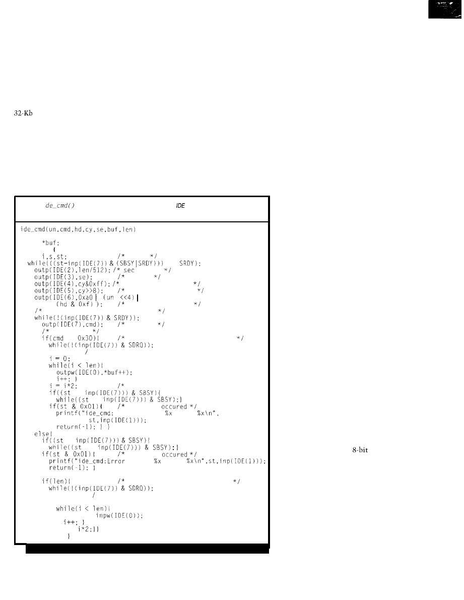
mostly in C, with some of the start-up
and exception processing routines in
68k assembly language.
The complete monitor may seem
fairly Spartan since it doesn’t imple-
ment fancy command-line editing,
history functions, or even a program-
ming/scripting language. However, if
you consider that it fits in a single
EPROM, you’ll realize it gets a
fair amount of bang for the buck.
Let’s look at the monitor’s operation
and features in more detail. At reset,
the 68030 expects to load the system
stack pointer at location 00000000 (hex)
and the initial PC at location 00000004.
Besides these vectors, many exception
vectors reside below 00000400.
The reset vector causes the CPU to
start executing the cold-reset start-up
code. The first thing the start-up code
does is to disable interrupts. While the
interrupts are already off after a real
reset, this task enables any code to use
the reset vector (which is in a known
location) to cause software to give up
control and reset the system.
Once the interrupts are off, the
monitor checks whether it’s already
running from DRAM by checking the
actual running address in the PC against
the desired address the monitor was
linked for. If the addresses don’t match,
the monitor copies the desired address
to DRAM (at physical address 80000000
[hex]) and resumes operation there.
Listing l-i
tries to read or write a block of data from the
hard disk by first seeking the
location and then reading or writing the disk data through the data port.
int un,cmd,hd,cy,se;
short
int len;
int
busy?
!=
count
sector
cylinder low byte
cylinder high byte
secsize,unit,head
wait for drive to become ready
command
do a write
==
wait for drive to accept data
len = len 2;
wait for completion of write here? *
=
=
an error
Error status error
=
=
an error
status error
i = st:
is drive ready to send data?
len = len 2;
i = 0;
*buf++ =
i =
return(i);
The code also changes the base of
the exception vector table to start in
DRAM. There are several reasons for
this.
Since the boot PROM is an 8-bit
device, execution speed is enhanced if
it’s copied and run from 32-bit-wide
DRAM. Also, DRAM makes it easy to
alter the exception-vector table and
patch the monitor code to add support
for new devices and fix bugs if needed.
After the monitor and exception
table is relocated, the assembly-lan-
guage start-up code is done and the C
code is called. If it’s the first time into
the monitor code after a real hardware
reset, the monitor initializes all the
needed I/O devices and prepares itself
to boot from the IDE drive unless the
user enters a character to interrupt the
auto-boot sequence.
If the auto-boot sequence is inter-
rupted in time, the monitor enters a
command-line-based interface so the
user can execute monitor routines to
boot from an alternate device or debug
a program. If the monitor is entered
from either a software-initiated reset
or an exception that isn’t trapped by
another program, the auto-boot se-
quence is bypassed and the command
loop entered directly.
The code also prints out the current
state of the PC and status register and
what exception caused control to be
transferred to the monitor. This sce-
nario occurs when a user program en-
counters an exception (e.g., an address/
bus error or divide-by-zero) or when an
unexpected interrupt occurs.
Let’s look at what it takes to boot
the system from one of the boot devices.
The monitor is supported for booting
from an AT-compatible IDE drive and
floppy drive on the ISA bus. It also
knows how to boot from Ethernet us-
ing one of two possible
Ethernet
card types (also on the ISA bus).
Booting from a disk device is rela-
tively straightforward. The monitor
reads the first sector from the floppy
or IDE drive to location 80008000
(hex) and extracts the number of
blocks and location on the media to
start reading the boot image.
The format of the boot sector looks
like Table 1. After loading the boot
sector, the monitor continues to read
Circuit Cellar
INK@
Issue 87 October 1997
6 7
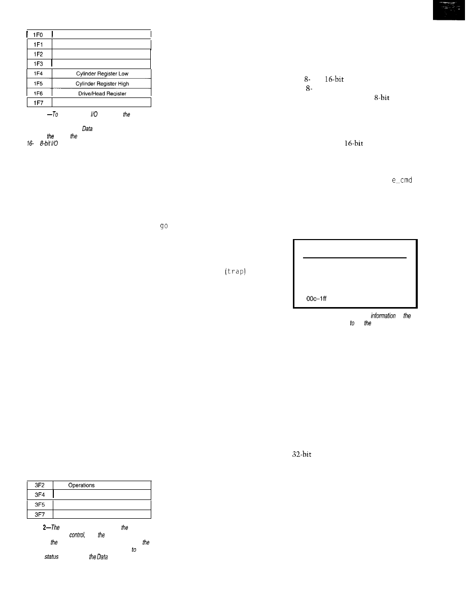
Data Register
Error Register
Sector Count Register
Sector Number Reqister
Status/Command Register
Figure 1
perform a disk operation, sector
location address must be programmed before a com-
mand can be given. The
register is 16 bits,
whereas resf of registers can be
accessed via
or
instructions.
the boot image until all specified blocks
are read.
Once the boot image is in memory,
the monitor does the equivalent of a
subroutine call starting at address
80008000. There, a branch instruction
should cause execution to continue
somewhere in the boot image, depend-
ing on the application.
The Ethernet boot code is similar. It
uses standard Internet protocols to
determine the boot image’s location
and filename on the network and uses
another standard protocol to download
the image to location 80008000.
Once loaded, it executes a subroutine
call to the start of the boot image. This
way, the same boot image can be loaded
from floppy/IDE and Ethernet without
changes to the image. In Part 3, I’ll
discuss the protocols used in loading
the boot image over the Ethernet.
Once control is given to the boot
image (usually some kind of operating
system), you only get back to the moni-
tor if an unexpected exception occurs
that the OS can’t handle or if the OS
gives control back to the monitor.
When students are learning to write
code for this system, we need to load
code images and allow debugging from
the monitor code. The student normally
assembles and compiles code on a
workstation and manages to get the
Control Register
Master Status Register
Data Register
Data-Rate Register
Figure
Operations register
resets controller
and spindle-motor
while Data-Rate register
programs data rate
and density desired. Most of
control is accomplished by sending commands and
reading
packets from
register.
code image into system memory for
debugging. (More on how the program
image gets there next time.)
The monitor’s debugging facilities
are Spartan so the student is exposed
to a different environment than they’re
used to. Since the lab’s purpose is to
teach computer-science students com-
puter architecture, we want them to
see low-level machine constructs. We
hope they learn how abstract program-
ming constructs in C/C++ programs
are implemented.
They’d also never experience the joy
of doing a manual stack trace to figure
out where their program bombed.
Remember, this lab is as close as most
computer-science students get to pro-
gramming real hardware these days.
After they load a code segment into
memory, they can use the monitor’s
command to start executing at a
specified address. They may also set a
breakpoint anywhere in their code.
When the processor encounters a
breakpoint, which is implemented with
a software interrupt
instruction,
an exception control jumps back to the
monitor where the context of the run-
ning code is saved. The user can then
examine and modify registers as well as
memory and continue executing their
code. The user can also trace their
program’s execution, for which the
68030 has a special hardware facility.
Another useful feature of the moni-
tor PROM is the ability to save more
than context. This feature enables the
student to save the context of an OS, if
active, and the context of the program
being debugged. There are two default
contexts for this purpose and a shortcut
command that restores the OS context
and continues execution.
DEVICE DRIVERS
Of course, the monitor also has to
implement device drivers for several
devices that are present. I already dis-
cussed the boot sequence, so let’s look
at some of the low-level routines used
to implement the device driver for the
boot devices.
The IDE controller contained on the
disk drive uses a parallel port on the
IDE interface card to connect to the ISA
bus. Last month, I talked about how
the ISA-bus interface is implemented.
To understand how the software
works, you only need to know that the
ISA bus is divided into four different
memory areas depending on what type
of ISA-bus bus cycle is required. These
are and
memory space access
and and 16-bit I/O access.
The IDE interface uses
I/O
accesses to communicate with its
registers. The register map and I/O
locations for the first IDE drive can be
seen in Figure 1. The data is transferred
through a single
I/O register
using programmed I/O.
Listing 1 starts the sequence of steps
necessary for reading from and writing
to the IDE disk. The routine
i
d
sets
up the IDE controller with the
desired disk address by programming
the appropriate register.
When reading, initiate the command
and poll the status register until the disk
Address
Description
000 (hex)
Branch to start
004 (hex)
Starting block number of
boot image
008 (hex)
Number of blocks in
boot image
Not used by monitor
Table 1 --The
boot sector contains
for
boot loader about
where find boot image and how
long if is.
drive is idle. Then, check the status
register for any errors. If none are found,
read the data from the data register.
For writing, the data should be trans-
ferred through the data register before
issuing the w r i t e. The data is simply
read or written to the data register
until the required amount is transferred.
The floppy driver is a bit more com-
plicated since some timing issues are
involved. The floppy driver is another
reason why we want to execute from
memory and why the monitor
was moved to DRAM.
It would have been possible to write
a floppy driver that ran from 8-bit
memory. But, it would have required
extensive assembly-language program-
ming to make it work fast enough
during the data-transfer phase.
The data-transfer phase involves the
most critical timing. There’s only a
single register to buffer the data to and
from the floppy disk.
68
Issue
87 October 1997
Circuit Cellar INK@
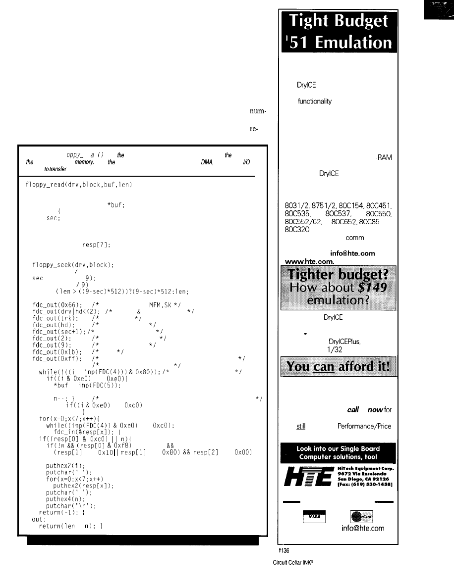
If we’re too slow in reading the
data, the data coming from the floppy
disk overruns the data register, causing
an error. If we’re too slow in writing
the data to the floppy, the data register
is empty when data needs to be serial-
ized to the floppy disk, resulting in a
data underrun. In a real PC architecture,
the DMA offloads the CPU from these
timing requirements.
the spindle. However, if it runs all the
time, the media can become worn out.
So, the motor needs to be started
before any floppy operation can proceed.
It also needs to be stopped sometime
after the last floppy operation is done.
Other than that, the floppy works
mostly like the IDE drive. The driver
calculates the sector number, cylinder,
and head number from the block
Motor control brings up another
ber requested, sets these parameters
complication on the floppy controller.
into the appropriate register, and
The floppy drive has a motor to drive
quests a seek operation.
Listing 2-f
7
r e d seeks specified location on the disk and then transfers data from
floppy data port to
Since 68030 motherboard doesn’t implement
programmed is
required
the data.
int drv;
unsigned block;
register unsigned char
int len;
int
int trk;
int hd;
register int n;
unsigned char
unsigned short x;
register unsigned char i;
trk = block 18;
= (block %
hd = (block % 2:
len =
n = len;
read command
drive head select
cylinder
head address
sector address
sector size 512
end of track
gap
data length, only if sector size == 0
while(n){
anything happening?
=
still executing
==
=
b u f + + ;
oops, not executing, must be response data
else
==
break;
!=
== 0x40
==
==
==
got0 out;
8051 Family Emulator is
truly Low Cost!
The
Plus is a modular emulator
designed to get maximum flexibility
and
for your hard earned
dollar.
805
1 f a m i l y
processor pods that are low in price.
Features
include:
Execute to
breakpoint, Line-by-Line Assembler,
Disassembler, SFR access, Fill, Set
and Dump Internal or External
and Code, Dump Registers, and
more. The
Plus base unit is
priced at a meager $299, and most
pods run
only an additional
$149.
Pods are available to support the
1 ,
and more. Interface through
your serial port and a
program.
Call for a brochure or use INTERNET.
We’re at
o r
Our
$149
model
IS
w h a t
you’re looking for.
Not an evaluation
board much more powerful. Same
features as the
but limited
to just the 803
processor.
So, if you’re still doing the
U V
Waltz (Burn-2-3, Erase-2-3). or
debugging through the limited window
ROM emulators give,
us
relief! Our customers say our products
are
the
best
emulators available!
S i n c e 1 9 8 3
(619) 566-l 892
VISA
Internet e-mail:
World Wide Web:
www.hte.com
Issue 87
October 1997
69
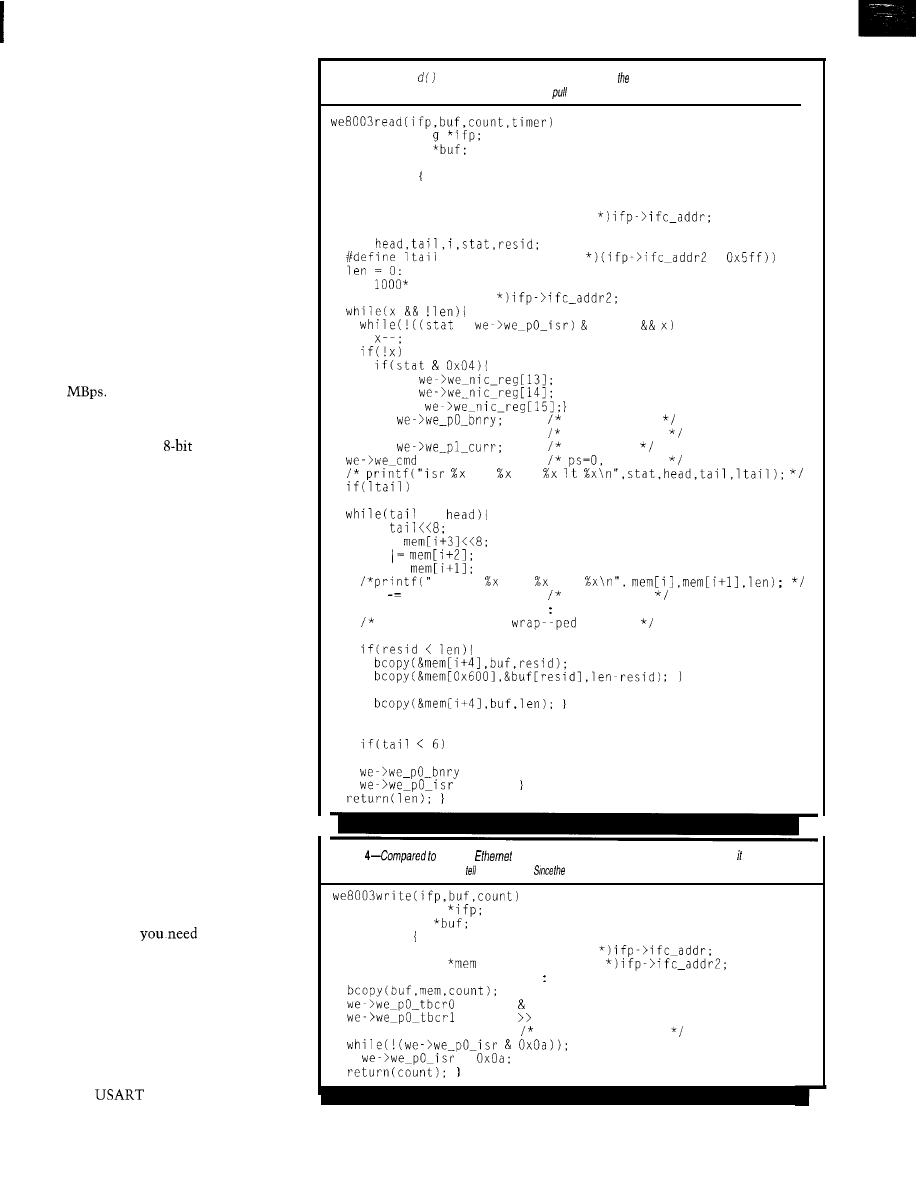
Once completed, the data can be read
or written to the data register. But, you
need to make sure the floppy is ready
by read-testing the data-request status
bit. Listing 2 shows the code for reading
one sector from the floppy, while Fig-
ure 2 shows the I/O register layout.
ETHERNET CONTROLLERS
Now that you know how to control
the floppy and IDE drive, what about
an Ethernet device? Ethernet controllers
are a bit more complex even at the
hardware level. Let’s examine the code
that sends and receives a packet on one
of the controllers.
Ethernet runs at 10 Mbps, which
turns out to be a little better than
1
Since many Ethernet packets
are not for this node, it’s wasteful to
get the processor to read every packet.
It would keep an
ISA-bus system
100% utilized whenever there’s traffic.
To reduce the I/O requirements,
Ethernet cards employ some kind of
buffer to store at least one received
packet. If this packet isn’t destined for
this station, the write point to the
packet memory is simply reset.
Once a packet is received, the Ether-
net card signals the processor with an
interrupt request or a bit in the status
register that it’s done. Listing 3 shows
the code for receiving a Ethernet packet
from an Ethernet card.
Sending packets is easy. The CPU
copies the packet to be transmitted to
the card’s transmit buffer and tells it
to start. If the Ethernet card transmits
the buffer, it simply indicates that it’s
done and interrupts.
Transmitting the packet can take a
long time. The card has to find an idle
period on the Ethernet and then try to
transmit. If another station tries to
transmit, a collision occurs and both
cards retry after a randomized timeout.
These actions are transparent to the
software, but
to be aware of
them, since it may take a while before
the transmit request completes. Check
out the transmit routine in Listing 4.
KEYBOARD
In Part 1, I talked about the physical
interface of the keyboard, which in-
volved how the data and clock interface
to the
in the 68901 MFP chip.
70
Issue
87 October 1997
Circuit Cellar INK@
Listing 3-we8003
re a
pulls a received Ethernet frame from Ethernet card’s infernal memory. Since
frames are stored in a circular queue on the card, the oldest frame and advance the tail pointer for another.
struct ifconfig
unsigned char
int count:
int *timer;
int len;
unsigned long x;
struct we8003 *we = (struct we8003
unsigned char *mem;
int
(*(unsigned char
+
x =
*timer;
mem = (unsigned char
=
0x05)
break:
i =
i =
i =
tail =
first packet
we->we_cmd = 0x42:
ps=l, running
head =
next free
= 0x02:
running
hd tl
len = len > count ? count len;
need to check for
buffers
resid = WE_MEMSIZ-i-4;
else
ltail = tail:
tail--:
tail = Oxlf;
= tail:
= Oxff;
tail = ltail;
!=
i =
len =
len
tail =
stat nxt len
len 4;
lop off CRC
Listing
reading
frames, sending
them is straightforward. Just copy to the Ethernet
card’s internal memory, and it to go.
monitor uses polling, wait here to make sure if was sent OK.
struct ifconfig
unsigned char
int count;
struct we8003 *we = (struct we8003
unsigned char
= (unsigned char
count = count > 60 ? count 60;
= count Oxff;
= count 8;
we->we_cmd = 0x06;
transmit, running
=
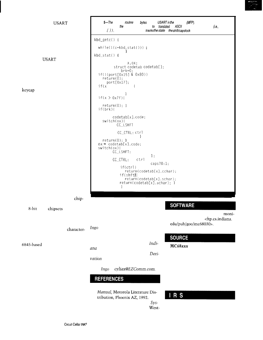
On the software side, the interface
looks like a standard
interface.
When a byte arrives from the key-
board, the receive-buffer fill bit gets set
in the status register and an interrupt is
generated when enabled. Reading the
received byte from the data register
resets the receive-buffer full condition
and readies the
for another byte.
It seems simple, but the received byte
is only the scan code from the keyboard
or, worse, one byte of a multiple-byte
message. What the monitor really needs
is an ASCII character that responds to
the
legend on the keyboard.
The keyboard driver achieves this by
looking up the scan code-one for each
key-in a character table. The driver
also tracks the state of the keyboard
shift and control keys, which modify
the ASCII code. Listing 5 explains all.
VGA DRIVER
Of course, I saved the hardest until
last-the VGA driver. It’s hard because
each VGA chip and card has a different
low-level configuration register set.
In the PC world, this situation is
handled by calling the appropriate ini-
tialization and mode change routines
from the BIOS on the card itself. The
code is usually proprietary, and I’d need
an Intel instruction emulator for my
system to execute the routines.
I ended up writing a driver for only a
limited number of possible VGA
sets, including the Paradise and Western
Digital
VGA
for which I
already had extensive datasheets. Other
chips/cards may also work if they
behave like a Western Digital chip.
The monitor only needs a
based interface, so I initialize the VGA
chip to its CGA mode, which emulates
the
CGA card. The moni-
tor then has a character-based frame
buffer with 8 KB of video RAM. To
speed up scrolling, the monitor’s char-
acter-output routine uses the extra
display memory to page the display.
UNTIL NEXT MONTH...
I hope I’ve given you an idea of how
involved even a simple debugging
monitor can become-without even
trying.
Next month, I’ll discuss the soft-
ware-development environment the
Listing
keyboard
pulls
from the
MC68901
These bytes are fhe
scan codes
from keyboard and need be
info
codes using a look-up fable
co de tab
The receive routine a/so
of
and control keys.
unsigned char c;
return(c);
unsigned char *port = KBD:
unsigned char
extern
static int
x =
== SC-BREAK)
brk = 1:
return(O);
brk = 0;
brk = 0;
ox =
case
case CC_RSHFT: shft = 0: break;
case
= 0; break:
default: break;
case
case CC_RSHFT:
shft = break;
case
= 1; break;
case CC-CAPS:
caps =
break;
default:
caps)
return(O);
students and
I
use to write software.
I’ll also tell you about some of the
things we’ve accomplished with this
system.
q
Cyliax is a research engineer in
the Analog VLSI and Robotics Lab
and teaches hardware design in the
computer-science department at
University. He also does software
and hardware development with
Systems, a San Diego-based
formal-synthesis company. You may
reach
at
Motorola, Programmer’s Reference
Complete source code for the
tor can be found at
Motorola
MCU Information Line
P.O. Box 13026
Austin, TX 78711-3026
(512) 328-2268
Fax: (512) 891-4465
freeware.aus.sps.mot.com
Western Digital, 1992 Devices,
425 Very Useful
tern Logic, Imaging, Storage,
426 Moderately Useful
ern Digital Corp., Irvine CA, 1992.
427
Not Useful
72
issue
87 October 1997
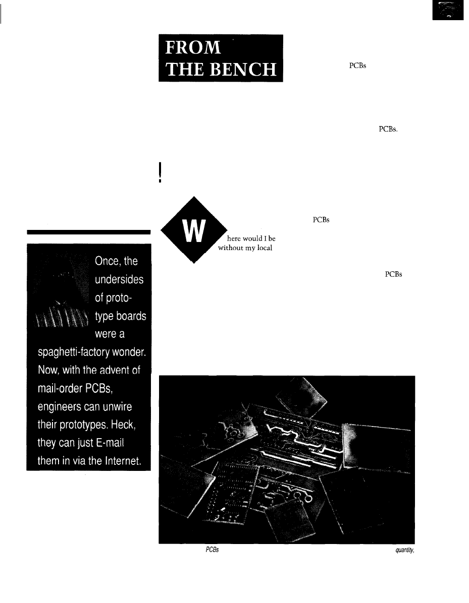
Prototypes of the Rich and
Famous-Not
Jeff Bachiochi
Radio Shack-or for
that matter, the mail-order
Digi-Key, Jameco, and Mousers who can
get me those low-quantity parts fast?
We’d all be in deep trouble without
access to these stores. Taking our
pencil-sketch designs into 3D reality is
what gets an engineer’s blood pumping.
The engineer is like the painter, and
the PCB is his canvas. Both begin with
blank panels and end with a work of art.
Wiring up a prototype without a
PCB is a laborious task. Although tools
abound to make the task a wee bit
easier, nothing lends itself more to
circuit legitimacy than a real PCB.
Unfortunately,
seem to be
like some of those specialized elec-
tronic parts that can only be obtained
in high quantities or in high-priced
evaluation units by big-name compa-
nies. But, what mail-order has done for
the availability of electronic parts it
has now done for prototype
MAIL-ORDER BRIDE
Not looking for a mate, you say, but
you could use a good prototype PCB if
it wasn’t too expensive? Well, listen up.
You no longer need to order a hun-
dred pieces. Now, there are many shops
around the country who specialize in
making a few quick, inexpensive, pro-
totype
of your design.
Around the country is not as far
away as you might think. Everything
can be handled over the phone-be it
sending your photoplot files directly to
the service’s BBS or indirectly to its
Internet site. In just days, the
are
delivered directly to your door via mail
or special carrier [see Photo
1).
Let’s look at the process in a little
more detail, and then maybe you’ll feel
comfortable enough to explore it on
your own.
SHOP SHOPPING
Don’t expect to find a PCB shop
next to the l-hour Moto-Foto at the
Photo 1 -Prototype
of various sizes don’t have to cost an arm and a leg. Depending on the size and
many boards are under $100.
74
Issue
87 October 1997
Circuit Cellar INK@
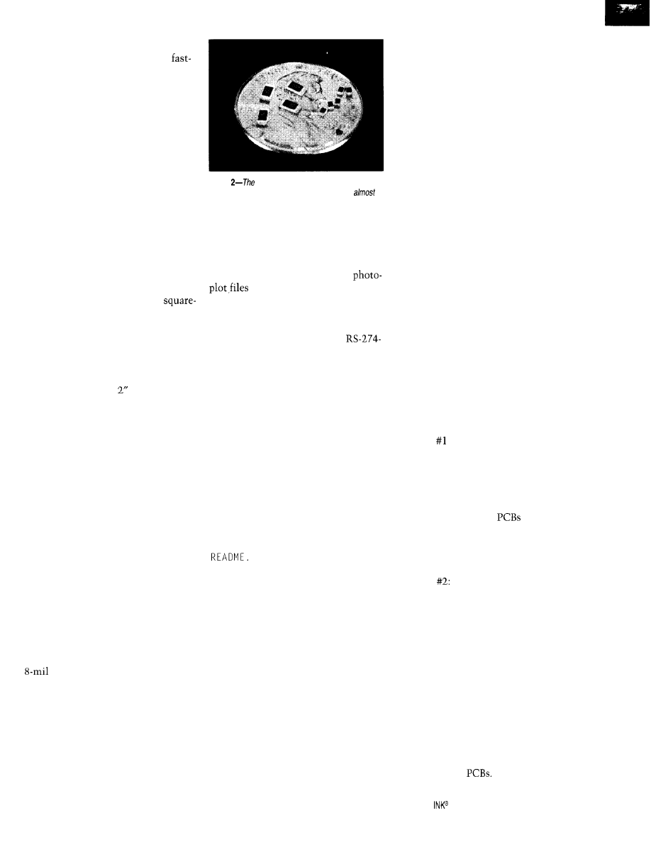
nearest mall. I get direct mailings, card
decks, and magazines advertising
turn proto-board houses every month.
The magazine you’ve got in your
hands right now has a few choice fabri-
cators advertising in the back pages.
You’ll find information easy to gather,
as many have Web sites promoting
their services.
Getting quotes isn’t really neces-
sary because the costs are spelled out
for you. Use the given formula for
estimating your own costs.
You’ll find cost to be based on two
factors-a flat fee plus a cost per square
inch. The flat fee pays for the labor
involved in preparing your zipped files
for processing. The cost per square
inch pays for the materials and labor to
fabricate your PCB.
Usually, there’s a minimum
inch buy, but unless you’re getting
very small boards, that’s generally not
a problem. For instance, a couple of
5” x 7” boards will set you back less
than $100.
That 70 in.2 of PCB can be divided
up into 10 pieces of a x 3” board.
Remember, the total area is made up
of not only usable board space but also
the waste area around the PCB that
will be whacked off.
So, what do you get for your Ben
Franklin?
Although not every PCB house plays
by the same rules (visit their Web site
or BBS, or call for the real scoop), you
will basically get a double-sided PCB
sheared (not routed) to roughly your
external dimensions (four straight
cuts).
The PCB will have plated through
holes drilled to a maximum density of
about 24 holes per square inch. You
may be limited to particular drill sizes
or a maximum number of drill changes,
so read carefully. Exceeding the rules
may cost you additional dollars.
Minimum technology is generally
traces and 8-mil spaces. That’s
0.008” minimum trace width with a
minimum 0.008” clearance around
everything.
Although soldermasks and silk-
screens aren’t included in this price,
they can be obtained for an extra fee. I
don’t get either of these on my proto-
types.
Photo
1210
and 0603 sizes practical/y disap
pear on the face of Abe Lincoln. Tiny park are
impossible to p/ace by hand.
PLAYING BY THE RULES
One of the first things you’ll find is
that all this works only if you play by
the rules and give these vendors
in a format they can work
with. The rules are spelled out rather
completely-often with examples.
However, they can be a bit heady if
you don’t know the lingo (e.g.,
D format).
Essentially, all files must contain
only ASCII information. The files you
need to include to the vendor for this
basic service are the photoplot files of
the top and bottom layers, the aperture
list for those plot files, the NC drill file,
and the tools list for the NC drill file.
The aperture list indicates which
size and shape drawing tool to use for
each of the photoplot steps to create
your top and bottom layers. The NC
tool list tells which drill sizes should
be used at each of the NC drill-file
coordinate locations.
In addition to these five files, a
TXT
file is often included.
This file is generally an order form
which spells out exactly what you’re
asking for, which pieces you’re provid-
ing, and how you’ll pay for it.
Believe it or not, this can some-
times be the most important file of all.
If problems arise, it might be your only
bargaining tool. Zip these files together,
and you’re ready to cast your design in
FR4.
WHAT, NO LAYOUT TOOLS?
You’ve always wanted to get a pro-
totype PCB but couldn’t afford the cost
of the layout software? Well, there
seems to be a new wave of inexpensive
CAD tools out now.
Almost all the mail-order parts
suppliers offer inexpensive software
packages. While you’re visiting Web
sites, be sure to check around the site
for free public-domain software.
Yup, you heard right. Free. Don’t
expect to get all the latest super tools,
but you should be able to create excel-
lent PCB designs and output the neces-
sary files for the fab house.
COMPONENTS AND TECHNOLOGY
Many think surface-mount compo-
nents come in a single size-small. But,
there’s small, and then there’s tiny.
The size you choose may have more to
do with the technology PCB you’re
shooting for than the absolute mini-
mum real estate a component takes up.
Take a look at the SMT resistors in
Photo 2. The sizes range from 25
12
down to 0405. These numbers tell
their own story. They are the length
and width of the component in milli-
meters. One can hardly pick up the
smallest with tweezers.
As parts become smaller, pick and
place equipment needs to be more
sophisticated. So, some vendors won’t
be able to work with some parts.
Warning : If you plan to use a spe-
cific assembly house sometime in
the future, make sure they can
handle the parts you’ve chosen in
your design.
The least expensive
are single
sided. These boards have traces on one
side only and any through holes have
no plating.
Warning
Provide sufficient pad
sizes. Inexperienced designers of
single-sided boards tend to forget
that without enough copper pad,
stresses will fatigue the bond be-
tween the copper and the fiberglass.
Since the through holes are not
plated, all the mechanical stress of a
component’s lead is placed on the adhe-
sive strength of the solder pad. A nor-
mal-size pad is too flimsy and doesn’t
provide adequate mechanical strength
for those heavy components.
Small SMT circuits can be designed
on single-sided
The larger SMT
Circuit Cellar
Issue 87 October 1997
75
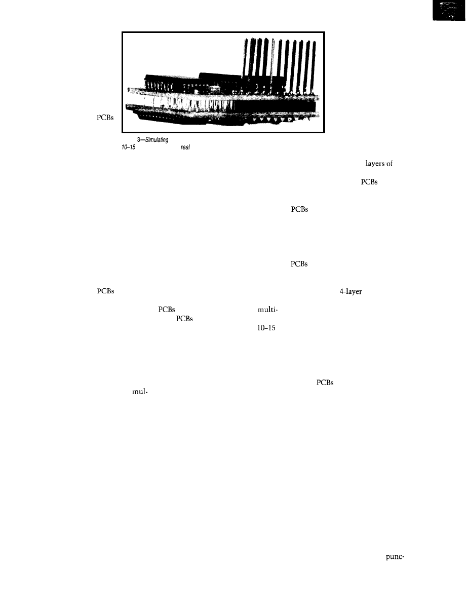
parts are valuable here since
their pads are far enough
apart to allow traces to
route underneath them,
avoiding the need for jump-
ers (i.e., those nasty extra
components necessary to
get a signal across a busy
maze of traces).
The most common
today are double sided. This
technique requires through
holes to be plated with
Photo
a
four-layer board can save a lot of money. You can expect to pay
times as much for a
four-layer prototype.
copper, making an electri-
cal connection from the trace on one
side to the trace on the opposite side.
This task is performed before any
copper has been removed on the outer
surfaces. The solid copper surfaces give
a path for current necessary in electro-
plating the holes.
Plated holes also give through-hole
components a good mechanical as well
as electrical bond to the PCB. Capil-
lary action enables solder to wick up
through the holes, making a fillet of
solder around the component lead on
top as well as on the bottom of the PCB.
While double-sided
are more
expensive, the layout can be crammed
together a lot tighter, in effect giving
you a smaller PCB. In the case of SMT
parts, the double-sided board lets parts
be mounted on both top and bottom.
But, that doesn’t mean twice the
parts in the same space. After all, some
real estate must be set aside for com-
ponent interconnections.
Although a double-sided PCB might
be considered multilayer, usually
tilayer refers to more than two layers.
A designer might need to use more
than two layers for a couple of reasons.
First and most obvious, additional
layers mean additional real estate for
routing connections. Although the
inner layers cannot hold components,
this setup does not free the layer to
100% routing.
Vias or feed throughs must be used
to connect the components on the outer
layers to the interconnecting traces on
the inner layers, and these take up valu-
able routing space. So, as the number
of layers increases, the actual routing
space per layer goes down. Eventually,
adding more layers won’t increase the
available routing area at all!
76
Issue
97 October 1997
Circuit Cellar INK@
The second reason to go multilayer
is to add ground and power planes, The
addition of layers exclusively used for
power and ground can reduce the need
for as many decoupling capacitors,
which reduces EM1 and provides the
lowest resistance paths for power and
ground connections to the circuitry.
By removing the power and ground
connections from the outer layers, many
designs are simplified to the point that
the remaining connections can be
completely routed on the outer layers.
MULTILAYER t PROTOTYPE
q
$$$
Although double-sided prototype
have never been cheaper,
layer
are still prohibitively ex-
pensive. You can expect to pay
times as much for a four-layer PCB.
Many of the smaller fab houses don’t
even offer this service.
So, how can you have your cake and
eat it, too? Let’s start with a look at a
simple four-layer board and how it
might be constructed.
The layers from top to bottom con-
sist of an outside trace layer, inside
power plane, inside ground plane, and
outside trace layer. The design could
be through hole or SMT.
Through-hole technology entails
component leads piercing through each
layer. If the component does not con-
nect to power or ground, there must be
an annular ring (of no copper) around
the component’s lead on that particu-
lar layer, insulating it from the plane.
SMT technology eliminates the need
for component holes. SMT designs
only require a via (i.e., an unsupported
hole] when the component’s lead must
connect to a component or plane on a
different layer.
These vias need not
pierce all layers. This
setup can lead to some
interesting drill files
where each pair of layers
may have a different drill
pattern.
An edge view of the
four-layer board would
show alternating layers
of copper and fiberglass.
That’s four layers of
copper and three layers of
fiberglass.
So, you’d need three
PCB
material-either a double-sided PCB
with two single-sided
laminated
to the top and bottom, or a bare (no
copper) PCB with two double-sided
laminated to the top and bottom.
Although the second example is more
common, you should include a fabrica-
tion drawing so the fab house doesn’t
have to guess on the makeup.
Why am
I
discussing multilayer
when the inexpensive houses
don’t do more than double sided? If
you take another look at the second
example of the
construction,
you might get what I’m hinting at.
If you take your four-layer design
and prototype the top layer and power
plane on a double-sided PCB and ground
plane and bottom layer on a second
double-sided PCB, you’ll end up with
an inexpensive four-layer PCB. The
only drawbacks are that you must add
a center layer of insulation between
the two
and make a multitude of
interconnections.
As you can see in Photo 3, the black
plastic carrier of a square-pin sip header
spaces two boards about 0.1” apart. In
cases where thickness is not a problem,
the air space is plenty wide enough to
ensure that the inner layers don’t short
to one another.
Since this design is totally SMT on
both outer layers except for the header,
all the vias need to be soldered using
pieces of solid wire and clipped off
flush with the outer layers. There are
many materials (besides air) that you
can use as to insulate between the
inner surfaces (i.e., the power and
ground planes).
You want to choose a material which
doesn’t melt easily but which
without much effort. A good
source of this stuff is the material on
which some bacon is packaged. It en-
ables the boards to be sandwiched
rather compactly. Once all the inter-
connects are soldered, the SMT parts
can be added.
Although a printed copy of the
photoplot files works well, I like to
have at least two prototypes. One is for
assembly, and the second is to see
where the traces go once the first pro-
totype is assembled and I need to refer
to the inner layers or underneath a
component.
BEER-BOTTLE BUDGET
In these times of bigger, faster,
more complex computers, it’s nice to
know that smaller, fast, less complex
designs have a chance of making it in
our world.
In fact, if you look around at the
consumer items being purchased to-
day, you’ll see technology creeping
into every appliance. None are con-
trolled by high-power PCs but much
smaller micros.
Many times, micros are added to
help products conserve energy or pro-
vide a level of safety. These designs
start with people like you and me.
Now, we have access to professional
without the big bucks normally
associated with the real thing.
I’d like to thank these companies for
their service in giving the little guy a
chance. Try ‘em. You’ll like ‘em.
Bachiochi (pronounced
AH-key”) is an electrical engineer on
Circuit Cellar INK’s engineering
staff.
His background includes product design
and manufacturing. He may be reached
at
Mail-order prototype boards
AP Circuits
3112 40th Ave. NE
Calgary, AB
Canada
(403) 250-3406
Fax: (403) 250-3465
www.apcircuits.com
Capital Electra-Circuits, Inc.
7845-J
Rd.
Gaithersburg, MD 20879
(301) 977-0303
Fax: (301) 990-6715
sales@capitalelectro.com
www.capitalelectro.com
EP Circuits
5468 Highroad Crescent
Chilliwack, BC
Canada
(604)
Fax: (604) 858-7663
Circuits, Inc.
4372 Dawson St.
Burnaby, BC
Canada
(604) 294-332 1
Fax: (604) 294-3302
428
Very Useful
429 Moderately Useful
430 Not Useful
in
development
.
after!
3
PAR (32 BITS MAX)
-STANDARD PC BUS
-LCD, KBD PORT
BATT. BACK. RTC
IRQO-15 (8259 X2)
DMA 8253 TMR
-BUILT-IN LED
-CMOS NVRAM
USE TURBO C,
BASIC, MASM
RUNS DOS AND
WINDOWS
EVAL KIT
PROGRAMMER
-DOES
MEG EPROMS
-CMOS, EE, FLASH, NVRAM
EASIER TO USE THAN MOST
POWERFUL SCRIPT ABILITY
MICROCONT. ADAPTERS
PLCC. MINI-DIP ADAPTERS
-SUPER FAST ALGORITHMS
OTHER PRODUCTS:
8088
SINGLE BOARD COMPUTER . . . . . . . OEM
l 95
PC FLASH/ROM DISKS
16 BIT 16 CHAN ADC-DA
21 . . . . . 75
C CARD . . . . . . . . . . . . . . . . . . . . . 55 .
WATCHDOG (REBOOTS PC ON HANGUP) . . . . . 27 . . . . . 95
‘EVAL KITS INCLUDE MANUAL
BRACKET AND SOFTWARE.
MVS BOX 850
5
YR LIMITED WARRANTY
FREE SHIPPING
HRS: MON-FRI
EST
a
MERRIMACK, NH
.
(508) 792 9507
Circuit Cellar
Issue 87
October 1997
7 7
T o m
of Analog Hope
ve often lamented
the fact our creator
failed to make the
world TTL compatible.
Oh well, nothing to test your faith like
trying to get some balky op-amp
to deliver a little more signal and less
noise.
When it comes to analog, I often
feel like one of those meek citizens of
the future held hostage by machines
meant to serve but which turn on their
users when no longer held in check by
a dwindling priesthood of “old ones.”
In fact, it seems much of the trend
to replace analog with digital tech-
niques, theoretical advantages of the
latter aside, can be traced to the fact
that few really understand (and fewer
are being taught) the ever-more-forgot-
ten art of analog design. Whether it’s
software modems or MPEG decoders,
users would rather watch a variable
and change a line of code than fiddle
with a scope and fumble around with
resistors and caps.
Is it the end of the road for op-amps?
Will all signal processing devolve into
software? Or, is there perhaps a middle
ground that combines the natural
fidelity of analog circuits with the easy
design and debug of digital?
What might the latter look like?
Check out the Motorola Programmable
Analog Array to get a glimpse of the
possible digilog future.
DIGITAL
VU
The MPAA020 Field Programmable
Analog Array isn’t the first chip to
combine the digital
concept
with analog circuits. Credit for that
notable first probably goes to the IMP
EPAC
(see “EPAC Epoch,” INK
58) though, much as the famous PAL
was predated by ROMs and
earlier
providers of simple metal
linear arrays could also claim credit.
However, the MPAA arguably goes
further in mimicking its digital counter-
parts. Photo
1
gives you a
view.
The chip comprises a 4 x 5 array of
so-called
(Configurable Analog
Blocks), which are conceptual counter-
parts of Xilinx’s digital
(Config-
urable Logic Blocks).
The similarity continues with pro-
vision on both chips for block inter-
connection using a combination of
local global routing that accommodates
the tradeoff between wiring flexibility,
speed, and cost. On the MPAA, the
vertical lines represent local wires that
any adjacent block can connect to,
while the horizontal “long lines” span
the entire chip.
Most
and
supplement
their basic function blocks with robust,
flexible I/O drivers. The MPAA follows
suit with thirteen of them on the pe-
riphery of the chip.
So far, I think you can see the simi-
larity between the MPAA and digital
and
Just replace the
latter’s digital logic and I/O blocks
with analog variants, and you’ve got
the gist of it. It’s not surprising to find
that the MPAA configuration scheme,
relying on SRAM (6864 bits to be ex-
act) to establish the cell function and
interconnect, is quite similar as well.
TAKE A CAB
Question: If a digital
relies on gates as the basis for block
functionality, what should an analog
version
The answer is, of course, that ana-
log stalwart-the op-amp (see Figure 1).
Search the dark and dusty recesses of
your bookcase to remind yourself how
the components in the input and feed-
back path determine the gain. (I found
Howard M. Berlin’s Design Of
Amp Circuits.)
78
issue 87 October 1997
Circuit Cellar INK@
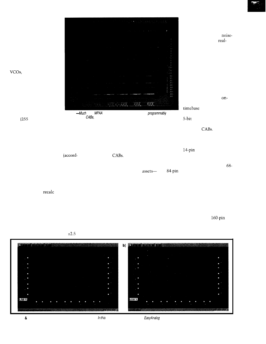
By configuring and com-
bining op-amps in different
ways, just about every in-
teresting analog circuit can
be concocted, including
filters (high, low, band pass,
and notch), function genera-
tors (sine, triangle, square,
ramp), peak detectors, recti-
fiers (half- and full-wave),
constant-current
sources, and so on.
Conventional op-amp
wisdom calls for resistors in
the feedback path. Instead,
the MPAA relies on
switched capacitors (five
per cell or 100 total per
chip) whose static capaci-
tance
levels) and
switching are both con-
trolled digitally. When configured and
switched appropriately, these capaci-
tors act as resistors and fulfill the role
of tuning the op-amp.
and 0 V, as well as an 8-bit program-
mable reference. There’s also an option
to provide an external reference input.
For utmost versatility, the references
are made available (i.e., routable) to
each of the 20
The MPAA generates an
internal 1 -MHz clock and,
as with reference voltages,
also accommodates an
external input. Once
board, this fundamental
goes through four
independent programmable
dividers, and the
various clocks are then
made available to the
Photo 1
of the
die area is consumed by wiring that
inter-
connects the 20
which are laid out in a pair of 2 x 5 strips.
PINS APLENTY
With conventional quad op-amps
available in
packages and given
that many of the connections are likely
confined inside the MPAA, you might
guess something along the lines of a
or
package would do the trick.
Thus, you-like I-might be a little
surprised to see the chip end up with
160 pins. But, whittle them down a bit,
and you’ll find the chip isn’t as impos-
ing as the package implies.
One interesting implementation
challenge that was overcome
ing to Motorola) is how to establish a
particular capacitor’s value in spite of
the variability imposed by the program-
mable interconnect. As you’ll see, the
MPAA development tools take care of
it automatically, so you don’t have go
through a tedious
every time the
design changes.
Typical analog circuits call for more
than just op-amps. For instance, any
comparison or limiting functions need
a reference against which to compare
or limit.
The MPAA offers a number of capa-
bilities in this regard, including
It might seem odd, but it’s a fact
that all but the simplest analog circuits
also call for that most digital of
a clock. After all, that’s where the
“switch” in switched-capacitor circuits
comes from.
Further, clocking is critical for
sampled-data circuits, particularly
filters, in which clock rate is a funda-
mental factor of merit. The well-known
Nyquist limit specifically states the
sampling rate must be at least twice
the highest frequency encountered in
the sampled data to avoid misleading
results due to aliasing.
However, it’s often over-
looked that the 2x factor is
impractically optimistic as
it needs a completely
free input. Add the
world’s complement of
glitches, drift, offset, and
quantization errors, and
you’ll find the sampling
rate should actually be
much higher.
First, there are a few dozen No
Connects, perhaps reserved for future
expanded parts, proprietary test access,
or just because there was a
fire
sale. Also, nobody with any analog
experience will complain about plenty
of provision (a dozen lines or so) for
a)
Photos 2a
b-Connecting wires is as simple as clicking the mouse.
pair of photos, notice how the
software doesn’t allow an invalid connection to be made.
Circuit Cellar INK”’
Issue 87 October 1997
7 9
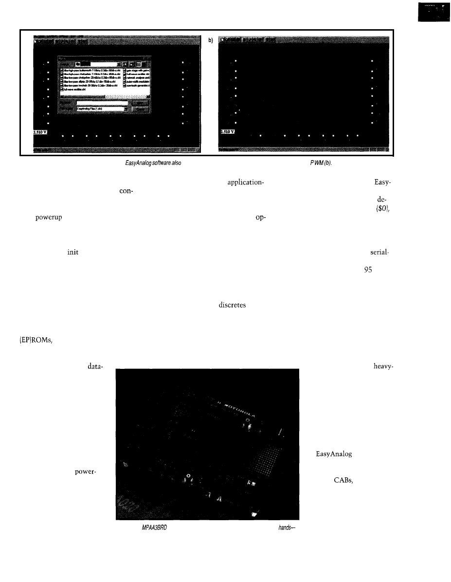
Photo
3-Beyond the one or two CAB macros, the
includes a library of even more complex cells (a), such as a
the separate analog and digital power
extra 8 uncommitted op-amps. The
Fortunately, Motorola offers handy
supplies.
latter are available for any
development software known as
Another major pin sink is the
specific use, but the external wiring
Analog. As the name implies, it goes a
figuration logic. Remember, since the
and resistors and so forth are up to you.
long way towards hiding the gory
MPAA is SRAM based, it’s brain dead
The I/O cells themselves are simple
tails. Best of all, the price is right
after
until all the SRAM bits
enough in concept, consisting of an
and your own copy is only a download
are set.
amp, programmable switch, and three
from the Web page away.
For the greatest flexibility, Motorola
offers a variety of ways to get inside
the MPAA and
the SRAM. The
particular approach used is determined
by strapping some mode pins.
As is usual for SRAM-based logic
chips, a serial EPROM works well. The
MPAA supports both those that require
an external address as well as those
with an internal-address generator.
lines. As you can see in Figure 2, be-
tween enabling and disabling the switch
connecting terminals x and y and the
op-amp, the I/O cells can be configured
as either input or output with or with-
out the op-amp buffering.
CONNECT THE DOTS
Thankfully, the software avoids the
bloatware tendencies and runs handily
on any ‘486, 4-MB RAM, VGA,
port box. I must sheepishly admit the
fact that it requires Windows did
set me back. I’m hoping to ride my old
‘386 Windows 3.1 box all the way to
Windows 98.
However, Motorola goes even fur-
ther by supporting generic byte-wide
though at the cost of 8 data
and
18
address lines. Why the chip
includes so many address lines isn’t
exactly clear from the
sheet. Perhaps another ex-
pansion plan down the road?
Replacing wires and
with
bits is fine, but only with good tools.
Only the most hard-core designer would
relish hand assembling the 6 Kb, pre-
suming they had the internal SRAM
address map, which wasn’t included in
the documentation I perused.
As you see from my photo, I have
enough gray hair already. Too many
more upgrade exercises, and I’ll be
hitting the Grecian Formula.
Fortunately, there’s no shortage of
bleeding-edge types here in Silicon
Valley, including my old friend Phil.
In any case, it’s simply a
matter of connecting up the
address and data lines, along
with provided control (e.g.,
*CE,
l
RD, etc.) lines, and
you’re in business. Natu-
rally, there’s also a RESET
line and the equivalent of a
sleep input that forces the
op-amp array into
down mode.
Ignoring all the baggage,
you’ll find the guts of the
MPAA boils down to three
lines for each of the previ-
ously mentioned 13 I/O cells
and three lines for each of an
Photo
4-The
Evaluation Board offers the opportunity to
gel
your
and
scope-on an MPAA.
He’s involved in some
duty I-way projects (not sure
exactly what, but mainly it
seems to involve “reinstall-
ing NT”) and has plenty of
the newest iron. Thanks to
Phil for helping me check
out the software (and Phil
thanks Motorola for includ-
ing an uninstall).
starts with
the basics-the ability to
establish the basic param-
eters for
I/O cells,
clocks, and so on, and man-
ually connect wires. Work-
ing at this level is still the
province of analog gurus,
though the software does
help a bit.
Circuit Cellar INK”
Issue 87
October 1997
81
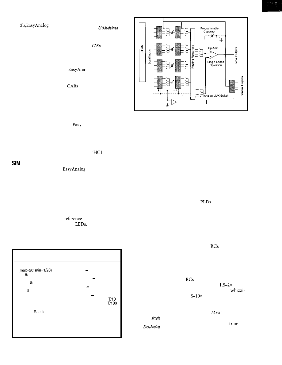
For instance, as shown in Photos 2a
and
w o n ’ t l e t y o u m a k e
an invalid connection or, similarly,
specify a cell characteristic that isn’t
possible. You can’t produce an invalid
configuration, though that doesn’t
mean your valid configuration will do
what you want.
As far as I, an analog neophyte, am
concerned, the real benefit of
log is the design expertise embodied in
the supplied macros (see Table 1). While
they do consume one or two
each, they also compose a rather com-
plete catalog of high-level functions.
As Photo 3a shows, these macros can
be further combined into cells (e.g., the
PWM in Photo 3b) included with the
Figure l--Each
CAB is
centered around an op-amp
with
charac-
teristics and interconnects
capacitors serve to tune the
function (e.g., setting
Control Logic
software.
role of an EPROM emulator, receiving
without complete knowledge of a
Once your design is entered,
the hex file of your design and imper-
Analog saves the corresponding SRAM
sonating the boot device the MPAA
bit file in a variety of formats (i.e., Intel
expects to find on RESET. Interest-
and Motorola hex, forward, and re-
ingly, the pod doesn’t actually use a
versed). One of these should be deci-
memory chip but instead coerces an
pherable by your EPROM programmer.
1
MCU into impersonating one.
OR EM?
I was disappointed that
doesn’t include a simulator. Instead,
instant gratification calls for an evalu-
ation board (see Photo 4) as well as the
means and will to cough up $1500.
The board basically provides a ver-
satile living space for the MPAA with
plenty of jumpers, breadboard area, and
niceties such as voltage regulator,
external clock, and voltage
not to mention the switches and
Along with the board comes a pod
that sits between it and your PC serial
port. In essence, the pod fulfills the
Motorola’s idea is the easiest way to
study the MPAA. Download a design
(only takes a few seconds even with a
lowly RS-232 port), hook up a function
generator and scope, and have at it.
Pondering the situation a bit, I real-
ized the digital and analog worlds are
unequally served by the emulator and
simulator concepts. For a digital PLD
or FPGA, a simulated 5-V system is
accurate even if the actual design ends
up running at 4.8 V with a bit of noise
thrown in for good measure. A 1 is still
a 1, and likewise for 0.
By contrast, it’s quite easy for an
analog simulator to get out of sync
particular system’s wiring, component
tolerances, temperature, noise, and the
like. In fact, Motorola points out you’ll
likely to have to go back and tweak
various parameters (e.g., gains, offsets,
references, etc.) once the actual board
is designed and the MPAA can be exer-
cised in place.
THE YOLK’S ON ME?
In the earlier article on the EPAC, I
put forth the proposition that “though
I might end up with egg on my face,”
the digilog revolution, with analog
equivalents of
and FPGA as the
foot soldiers, was underway.
So far, it seems things are lagging a
bit. Despite the IMP EPAC and now
the Motorola MPAA (along with a lot
of mixed-signal hype and hope), open
today’s electronic gadget and you’re
likely to find an analog section with a
sea
of op-amps and
little changed
conceptually from 20 years ago.
Macro Functions
Single-Cell
Two-Cell
Gain stages
Low Q Biquad Filter
(Hi or Lo Pass) 2 cells
Sum Diff Amps
Low Q Biquad Filter
(3 weight inputs)
(Notch, Bandpass) 3 cells
Sample Hold
High Q Biquad Filter
(Hi or Lo Pass) 2 cells
Track Hold
High Q Biquad Filter
(Notch, Bandpass) 3 cells
Integrator
Maximum Corner Frequency =
n-Path Integrator
Minimum Corner Frequency =
Differentiator
Limiter
Half-wave
Interpolator
Full-wave Rectifier
Schmitt Trigger
LPF Rectifier
Voltage-Controlled Oscillator
Cosine Filter
Sine-wave Oscillator
Decimator
Square-wave Oscillator
Bilinear Filter
Triangle-wave Oscillator
Table
l-Beyond
p/ace and route, much of the
value of the
early-and very pricey at the
software is incorporated in the
digital PLD and FPGA chips. Of course,
library of predefined macros.
the naysayers have long since gotten
To be frank, Motorola’s $50 price
tag for the MPAA doesn’t exactly prod
things along. Yes, the whole concept is
neat, but a couple dozen op-amps and
bag of
cost a lot less. Perhaps
many are willing to pay
for the
convenience, integration, and
ness, but
is tough to swallow.
Nevertheless, I remain hopeful,
mainly because I remember the similar
“it costs more than
complaint
levied against the suppliers of the
Circuit Cellar INK@
Issue 87 October 1997
83
General Software is the pioneer of embedded systems. Since 1989 our
software has been the core intelligence of miniaturization. From cellular
phones to the space shuttle, General Software enables dreams. Our new
Embedded BIOS” and Embedded DOS” systems will take your projects
farther faster than ever before.
If it’s time for a new design start, it’s time for General Software.
Call for information
on Embedded Systems:
800-850-5755
S O F T W A R E
Start the
Please visit our web site: www.gensw.com
DOS
are
Figure
13 cells comprise
pins, a
programmable switch, and yet another
buffering signals headed on-
or off-chip.
religion and, along the way, propelled
outfits like Xilinx,
Lattice, and
their kin to great heights.
For now, just remember, “Don’t put
all your eggs in one basket because you
don’t know whether the chicken or egg
is coming first and you shouldn’t count
your chickens before they hatch.”
By the time you figure out what the
heck that all means, I hope I can point
to an accelerating digilog revolution.
(Motorola’s already talking about
generation
Otherwise, all I
can say is that like ‘em over easy.
q
Tom Cantrell has been working on
chip, board, and systems design and
marketing in Silicon Valley for more
than ten years. You may reach him by
E-mail at
corn, by telephone at (510)
or by fax at (510)
H.M. Berlin, Design Of Op-Amp
Circuits,
Howard W. Sams and
Co., Indianapolis, IN, 1977.
MDEL612,
MPAA020
FPAA
Motorola
2100 E. Elliott Rd.
Tempe, AZ 85284
(602) 413-4663
Fax: (602) 413-4034
431 Very Useful
432 Moderately Useful
433 Not Useful
84
Issue 87 October 1997
Circuit Cellar
INK@
INTERRUPT
The People’s Contest
mentioned that we did a reader survey a couple months ago. It’s something we should do more often, but
given the hectic pace around here, tasks like these are as much a luxury as they are a necessity. Unlike an
advertising focused survey-you know, the ones that ask whether you prefer Brand A or Brand B products-this was
purely an editorial questionnaire. We asked things like what kind of processor you like and what technical subjects you’d
like to see covered in
We had a 50% survey response from our fantastically loyal audience.
One of the more interesting conclusions from the survey is that, while you have particular processor preferences, you appreciate the
diversity of selections available when designing embedded controls. Today’s technology has provided us with a plethora of processor and
cost options that must be duly considered (gone are the good old days when every embedded control problem could be solved with 64k on
an
processor).
Part of the survey asked what processors you’ve used, are using, or expect to use. Not surprisingly, the big winner in past applications
was the
and
Present applications seem to be evenly divided among
and
For the future,
however, the two winners are 80x86 (including Pentiums) and
admit right up front that from the old school. look at solving embedded control problems with a scalpel rather than a sledgeham-
mer. Being a realist, however, know that many applications are solved best with
and MMX technology. That practical realization is
the rationale behind our
Embedded PC section each month, and it was the impetus for our Embedded PC Design contest.
The wide disparity in processing power between
and Pentiums in future applications is not a simple issue of choice. It’s an
exercise in practical engineering. Not all problems are equal, and certainly no one processing solution is adequate. The
Embedded PC
Design Contest focused on demonstrating high-end problems and PC-based solutions. The response was significant, and you’ll soon see a
number of these entries as
With that concluded, we determined that our next contest should test the prowess of designers at the decidedly less expensive end of
the embedded solution spectrum. It only took a few E-mail messages back and forth for Microchip Technology to agree to sponsor the whole
contest. Certainly we had evidence of PIC popularity among the readership, but it was only coincidental and decidedly after the fact that our
survey results bear out the veracity in our choice of sponsors.
This month, Circuit
Cellar
Design98. Sponsored by Microchip Technology in association with Hewlett-Packard, Bell
Electronics, and Pioneer Electronics, Design98 gives you an opportunity to show the rest of us what can be really done with PIC processors.
Winning is a function of finesse and not complexity. Projects can range from the very simple to the most intricate. The deadline is March
1998, and we welcome entries that run the gamut. There are $23,000 in cash prizes alone. The contestant awarded Best Overall will
receive $5000 and a
Mixed Signal Oscilloscope. There are three design
and
first
($3000) second ($2000) and third ($1000) prizes awarded for each category. Plus there are cash bonuses if you design in some specified
components. Visit our Web site at
for contest rules and an entry form.
As the local lottery ads say, you have to play to win. And fortunately, design contests make us all winners in the end. Our survey ratifies
the popularity of the
and Design98 provides incentive to document really neat applications. The real reward
will
be when we read about
the winning projects in INK.
96
Issue 87 October 1997
Circuit Cellar
Wyszukiwarka
Podobne podstrony:
circuit cellar1990 10,11
circuit cellar2002 10
circuit cellar1996 10
circuit cellar1995 10
circuit cellar2004 10
circuit cellar1991 10,11
circuit cellar1992 10,11
circuit cellar1994 10
circuit cellar2003 10
circuit cellar1993 10
circuit cellar2001 10
circuit cellar2000 10
circuit cellar1990 10,11
circuit cellar1991 10,11
circuit cellar2003 10
circuit cellar1994 10
circuit cellar1997 10
circuit cellar1993 10
więcej podobnych podstron