
Journal, though, we’re already thinking about 1994.
The production schedule is finished and we’ve chosen the editorial themes
for the year. For the moment, let me ask that you remove your reader hat
and replace it with your author hat. Take a look at the following list of themes
and see if any matches your specialty or latest project:
Proposal
January
42
February
43
March
44
April
45
May
46
June
47
July
48
August
49
September
50
October
51
November
52
December
53
Deadline
Home Automation
911193
Applications in Light
1011193
Cross-development Tools
Graphics and Video
1211193
Robotics
Distributed Control
211194
Communications
311194
Data Acquisition
411194
Embedded Applications
512194
Industrial Control
611194
Digital Signal Processing
711194
Computing in Real Time
As I’ve said before, you don’t have to be a professional writer or even
have written an article before to write for us. What’s important is that you
know your stuff and you can describe it in a manner that your fellow
engineer can understand. Give me a call
send a fax (2031
write a letter (4 Park St., Vernon, CT 06066) or send me a BBS
message
988) with your ideas and we’ll see where it leads.
In this month’s feature articles, we have what I think is a neat project
that graphically illustrates an example of real-world interfacing and control.
The gas-fired foundry furnace controller collects information from an
assortment of sensors and must make an intelligent decision about whether
to allow the fire to burn. An error here could cause a bit more damage than a
runaway lighting controller.
Next, we’ve had numerous articles in the past on controlling stepper
motors, but now it’s time to bring on the big motors. Find out what it takes to
drive the motors that require more than a few milliwatts of power to operate.
Finally, Design Contest winner Derek Matsunaga describes how he
reverse-engineered a test feature found on several models of Fluke
multimeters so he could automatically send meter readings to a data
collection computer.
I look forward to hearing from you with your article ideas.
CIRCUIT CELLAR
THE COMPUTER
APPLICATIONS
JOURNAL
FOUNDER/EDITORIAL DIRECTOR
Steve Ciarcia
EDITOR-IN-CHIEF
Ken Davidson
TECHNICAL EDITOR
Michael Swartzendruber
ASSOCIATE EDITOR
Robert
ENGINEERING STAFF
Jeff Bachiochi Ed Nisley
WEST COAST EDITOR
Tom Cantrell
CONTRIBUTING EDITORS
John Dybowski Russ Reiss
NEW PRODUCTS EDITOR
Harv Weiner
PUBLISHER
Daniel Rodrigues
PUBLISHER’S ASSISTANT
Susan McGill
CIRCULATION COORDINATOR
Rose
CIRCULATION ASSISTANT
Barbara
CIRCULATION CONSULTANT
Gregory Spitzfaden
BUSINESS MANAGER
Jeannette Walters
ADVERTISING COORDINATOR
Dan Gorsky
CIRCUIT CELLAR INK. THE COMPUTER
J O U R N A L
monthly by
Cellar Incorporated. 4 Park Street,
ART DIRECTOR
Lisa Ferry
Suite 20, Vernon. CT 06066 (203)
Second
Vernon,
One-year (12
rate
and
GRAPHIC ARTIST
Joseph Quinlan
tries $49 95. All
orders payable in
funds only, via
postal money order or
check drawn on
bank
orders
CONTRIBUTORS:
Jon Elson
Tim
and
related questions to The Computer
Journal
P.O. Box 7694,
NJ 06077 or call (609)
POSTMASTER. Please send address changes to The
Frank Kuechmann
Computer Applications Journal,
Dept P 0.
Pellervo Kaskinen
Box 7694,
NJ 08077.
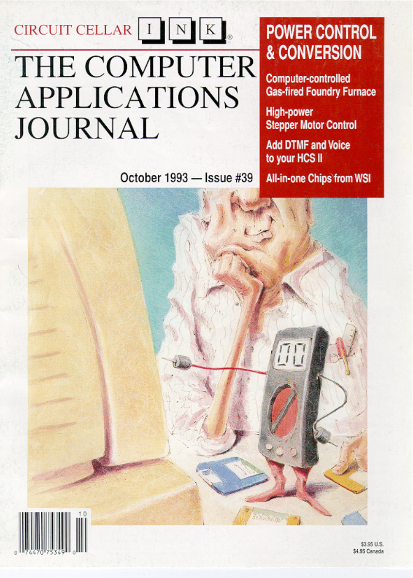
Cover Illustration by Bob Schuchman
PRINTED IN THE UNITED STATES
ASSOCIATES
NATIONAL ADVERTISING REPRESENTATIVES
NORTHEAST
Debra Andersen
SOUTHEAST
Collins
WEST COAST
Barbara Jones
(617)
Fax: (617) 769-8982
MID-ATLANTIC
Barbara Best
(305) 966-3939
Fax: (305) 985-8457
MIDWEST
Nanette Traetow
Shelley Rainey
(714) 540-3554
Fax: (714)
(908) 741-7744
Fax: (908)
(708) 789-3080
Fax: (708)
panty, 1 stop
9600 bps Courier HST. (203)
All programs and
Cellar
been
to ensure
performance
transfer by subscribers
no warranties and assumes no
or
of any
for errors in these
programs or
or for the consequences any such
Furthermore, because of
the quality and
of materials and workmanship
projects.
Cellar INK
any
the safe and proper
of reader-assembled projects based upon or from
plans,
or information published Circuit Cellar
INK
contents
1993 by
Cellar Incorporated. All
resewed.
of
whole or in
consent from
Cellar Inc.
2
Issue
October 1993
The Computer Applications Journal

1 4
Fire Control for Foundry Furnaces
by David
Stepping Up in Performance
by Tom Dahlin
Data Logging Meters are No Fluke
by Derek Matsunaga
q
Firmware Furnace
and
The ‘386SX Gets Positive
Identification and a Small Display
Ed Nisley
5 8
q
From the Bench
Updating TIM for the HCS II: Add the Touchtone
Interactive Monitor to your home control system
Bachiochi
q
Silicon Update
Swiss Army Chip
Tom Cantrell
q
Embedded Techniques
Small Memories
Dybowski
Editor’s INK
Ken Davidson
The Year Ahead
Reader’s INK
Letters to the Editor
New Product News
edited by Harv Weiner
Patent Talk
Reiss
Excerpts from
the Circuit Cellar BBS
conducted by
Ken Davidson
Steve’s Own INK
Steve Ciarcia
The
Race for Power
Advertiser’s Index
The Computer Applications Journal
Issue
October 1993
3

ONE COLLEGE STUDENT’S VIEW
Can you believe that? It takes 2% years to enter a lab.
I have been meaning to write to Steve ever since his
That’s crazy!
editorial on the importance of properly educating our
Therefore, how can I deeply respect American
future engineers and innovators. Your offer of magazine
colleges and their requirements? In Steve’s recent
subscriptions was most generous.
editorial, he tells us to study and take advantage of our
Who am I? I’m going to be a junior in the EE
classes. I see little to take advantage of. The way to learn
program at Cooper Union in New York City, but since I
is on your own through books, magazines,
and
was in fifth grade, I have been interested in and learning
experimentation. This must be encouraged by our
about electronics. Steve’s BYTE columns fueled my
society. Somehow.
quest for knowledge and I read them religiously from
I’m an academic “squeaker” as you put it. My
May 1987 until the founding of Circuit Cellar INK.
overall GPA is 3.1 and my major is 3.4. I’ll maintain
Your BBS was perhaps my most valuable resource
those, but no more unless by luck. The way I see it, I can
where real engineers helped a high school student find
keep those averages with minimal impact on my life.
the bug in his first 6808 computer board
were
That means plenty of time for my supercomputer
wired backwards to the
I did a good deal of
research, for airplane building and flying, for my
work with
microcontrollers before entering college
ests-my sanity. It is my belief that I will succeed
two years ago. Unfortunately, college took much of my
through hard work on my own as I pursue my interests
time as did my job in the computer center, so I haven’t
and gain valuable skills. We’ll see..
done any building since high school. My main computer
Thanks so much for your columns, your magazine,
interests are now centered on parallel supercomputing.
your BBS, and Steve’s personal answers to a
But I continue to have a soft spot for small
questions about TTL
People like you are true
lers. My new hobby, radio-controlled airplanes, provides
educators.
for many fascinating control projects.
Why am I writing to you? It’s the whole issue of
Mark
American education in the technology arena-it’s
Brooklyn, N.Y.
pitiful. What can I say? Much of what we’re fed in
college is inappropriate and is “taught” (to use the term
loosely) by
who are out of touch with industry,
After discussing your letter in the office among
creativity, students, and enthusiasm. This past summer,
several engineers with backgrounds similar to yours, we
I worked for two months at Sun Microsystems in
can sympathize with your frustration. “Why don’t they
Mountain View,
doing digital design work. I did
just get on with it and teach us something we’ll use in
this work with knowledge that I taught myself from
the real world!” We’ve all been through it. Contrary to
your projects, from other engineers, from reading, and
what you believe right now, though, those
from experimentation.
ate” courses that you think are a waste of time are
Two complete years of engineering college provided
actually laying the groundwork of knowledge that you
me with near zero. A basic circuits course and an analog
will rely upon, consciously or unconsciously, for the rest
electronics course accounted for college’s contribution
of your life.
to my usable skills. There is hardly any motivation
College is not for learning about and playing with
through hands-on engineering in school. So many smart
the latest chips or processors currently on the market. If
people are turned away from what I love because of
that’s all you graduated with, you’d be worthless ten
what they are presented at school.
years down the road when your sum total knowledge is
This has to change. Fewer theoretical formulas and
woefully out of date.
more wire-wrapping. Less cramming and more
College is where you learn how to learn. It teaches
ing. A student should be shown a data book freshman
you the problem-solving techniques and gives you the
year and learn about real components. Then, after a
basic skills that you’ll need once you make it into the
couple of years of fun learning, you introduce the heavy
real world. Hands-on learning and experience are
theory. It’s a tough situation.
something you’ll get in your first few years on the job.
EE students at my school (and others) do not enter a
There just isn’t enough manpower, resources, or time to
lab class until the second semester of their junior year.
include that kind of teaching in a four-year program.
6
Issue
October 1993
The Computer Applications Journal
INK
And until you decide what you want to specialize
in, it really isn’t even appropriate.
You trusted Steve as a
to answer your
question from his many years of experience. Trust us
again on this one. Go to class, do the work, and put your
heart and soul into it. You won’t have this opportunity
again. Once you graduate, you’ll have plenty of time for
supercomputers and model airplanes. Now is the time to
prepare for the future.
-Editors
SOFTWARE CONTROLLERS ON THE MAC
Regarding the letter from Fred Johnson in the July
issue in which he asks about development tools for the
Macintosh: HyperCard! It’s the cat’s meow. I’m not a
programmer, yet was able to easily develop a very robust
graphic robotic controller,
using HyperCard
and communicating via the built-in serial port. I even
built a radio link to sever the cord. The real beauty is
that HyperCard comes with the Mac.
If Fred has questions, I’m Sparky3 on America
Online.
Gene Simmons
Harvest, Ala.
CORRECTION
On page 12 of the September issue, the correct phone
number for Acuity Research Inc. is (408) 252-9639. We
regret any inconvenience this error may have caused.
We want to hear from you!
We encourage our readers to write letters of praise,
condemnation, or suggestion to the editors of the
Computer Applications Journal. Send your letters to:
The Computer Applications Journal
letters to the Editor
4 Park St.
l
Vernon, CT 06066
CIARCIA
DESIGN WORKS
Steve Ciarcia and the Ciarcia Design Works staff may have the
solution. We have a team of accomplished programmers and
engineers ready to design products or solve tricky engineering
problems. Whether you need an on-line solution for a unique
problem, a product for a startup venture, or just experienced
consulting, the Ciarcia Design Works is ready to work with you.
Just fax me your problem and we’ll be in touch.
Remember...a
design works!
F a x
(203) 871-8986
Embedded
P C
with on-board
Ethernet
and
Super VGA
l
25 MHz
CPU; including u
to 16 MByte DRA
l
On-board Super VGA
LCD/Video controller
On-board Ethernet, Featuring
AUI and 10 BASE-T interfaces
l
SCSI, Floppy, controllers and
2 MByte Flash Eprom Solid State Disk
volt only operation,
5 watts power consumption
Other features include:
3 Serial Ports,
port, BIOS, Real
Clock,
Bus Expansion
For more information call:
Megatel Computer Corporation
125 Wendell Ave., Weston, Ont.
Fax: (41612456505
The Computer Applications Journal
Issue
October 1993
7

Edited by Harv Weiner
EMBEDDED PC FEATURES LOCAL BUS
SUPER VGA
The embedded marketplace continually
pressures PC manufacturers to decrease size
while increasing functionality. Megatel has
responded with the PC/II+, an
PC compatible with a multitude of features on
a
PC/ 104 format board.
The PC/II+ includes a
processor
with up to
bytes of interleaved user
DRAM, 256K bytes BIOS flash memory, SCSI
host adapter, floppy disk controller, super VGA
video/LCD controller, and an AT-compatible
BIOS. Standard I/O features include two RS-232
serial ports, an RS-232 high-speed serial port,
general-purpose parallel I/O port with BIOS
support as a printer port, a real-time clock with
battery backup, and a
ISA
I/O bus. CMOS technology is extensively used to reduce power consumption to approximately 6 watts at
V.
The PC/II+ also includes an Ethernet interface using the Intel 82595 single-chip Ethernet controller and its
buffered slave architecture. Megatel supports both and
operations, both fully 802.3 compliant with the
and TPE serial interface. Software for the Ethernet interface includes full Novell
support.
The performance of the on-board display controller has been increased by implementing a local bus, Chips
Technologies 65530 super VGA controller with a full
byte of video RAM. This allows the use of many of the
higher resolution super VGA modes that are popular with multimedia applications.
Megatel provides a complete legal BIOS in flash memory. It will boot standard versions of PC-, MS-, or DR-DOS.
An on-board ROM DOS is also offered. The PC/II+ will run most of the popular PC software packages including
Windows 3.1. A high-performance flash-file subsystem, which provides on-board capability for a
solid
state disk, is also included.
The PC/II+ Developer’s Kit sells for $995. with 2M bytes of memory. The kit includes a passive backplane,
transition I/O board, cable set, board jacket, and user/technical manual set.
Megatel
l
125 Wendell Ave.
l
Weston, Ontario
l
Canada
l
(416)
l
Fax: (416)
PC VIDEO ON TV
A low-cost PC-compatible plug-in card and software that will allow
the display of computer screen images on a TV or their storage on an
SVHS VCR has been introduced by International Computers. The
is capable of displaying both VGA text and graphics on both
black-and-white and color screens. VGA cards capable of interlaced video
signals will be displayed on a TV set with perfect
resolution.
Noninterlaced video signals are also accommodated with excellent
results. The device can produce flicker-free images from Windows.
supports both text and graphics modes. Standard VGA
modes are used by all video card manufacturers, but some cards use
unique extended modes, with resolutions far beyond the original IBM
definitions.
features a lookup table to determine the proper
addressing and mode number for the VGA card installed.
A user’s manual and a video output cable to connect the unit to a TV or VCR are provided. The
includes the PC card, 2 video cables, user’s manual and software diskette, and sells for $99.
International Computers
l
12021 West Bluemound Rd.
l
Wauwatosa, WI 53226 (414) 764-9000
l
Fax: (414) 281-3522
October 1993
The Computer Applications Journal
CALLER ID ACCESSORY
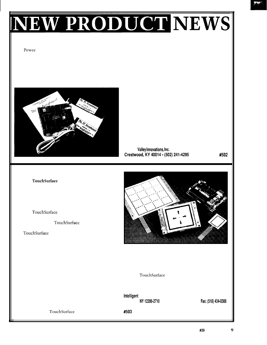
Valley Innovations has introduced a multi-
purpose, PC-based Caller ID accessory that offers
convenient and foolproof solutions to telephone-related
access and security problems. The PC Receptionist can
be used to restrict access to modems and fax machines,
track telephone usage, log customer and client calls, and
make efficient use of pager facilities.
Unlike many security systems that automatically
answer a call and wait for the caller to enter an access
code and/or password, the PC Receptionist uses Call
Block/Pass technology to completely eliminate any
chance of a hacker gaining access to the system. Unau-
thorized or unwanted calls are never answered and the
system can be configured to completely block calls from
predefined or unknown numbers, or to pass calls only
from particular numbers, or both. The PC Receptionist
is transparent to outgoing calls.
The PC Receptionist includes an easily configured
eight-bit slot adapter card for IBM-compatible comput-
ers, DOS software, users manual, and a modular exten-
sion cord. For full operation, Caller ID service must be
available from the local telephone company and sub-
scribed to by the user. The PC Receptionist hardware is
FCC Part 15 and Part 68 certified and is warranted for
one year. The PC Receptionist Kit for DOS sells for
$149.95. Windows-based software is $30 additional.
Pewee
l
6601 Old Zaring Rd.
TOUCHSURFACE DEVELOPER KITS
The
is a powerful, low-cost, input or
control technology that senses both position and
pressure continuously when touched with a finger or
stylus. Intelligent Computer Music Systems has
announced three developer kits for product design and
experimentation.
The
Demonstration Pointing Device
is a desktop computer peripheral that provides the
fastest evaluation of
technology. It is
suitable for developing product concepts and evaluating
the
as a pointing device or multimedia
controller with capabilities well beyond mice and
trackballs. It offers Microsoft two-button mouse
compatibility in MS-DOS and Windows, and is fully
user configurable in Windows.
The Panel Point is an embedded pointing device
module designed for mounting in a panel or in an
instrument chassis. It interfaces through a serial port
and is ideal for industrial controls, mobile computer
products, or other applications where control or
pointing device functions are needed, but a mouse or
trackball is inappropriate. Typical applications include
character or graphical user interfaces, real-time systems
controls, and absolute or relative positioning systems.
The Analog Interface Kit gives the product designer
or experimenter a
sensor with an analog
voltage output. Applications for such a device include
product development with embedded microcontrollers
and systems that already incorporate analog-to-digital
converters, or industrial or laboratory computers
incorporating data acquisition systems.
The
Demonstration Pointing Device
and Panel Point Developer Kit sell for $250 each, and the
Analog Interface Kit sells for $150.
Music.116
North Lake Ave.
Albany,
l
(518)434-4110
l
The Computer Applications Journal
issue
October 1993
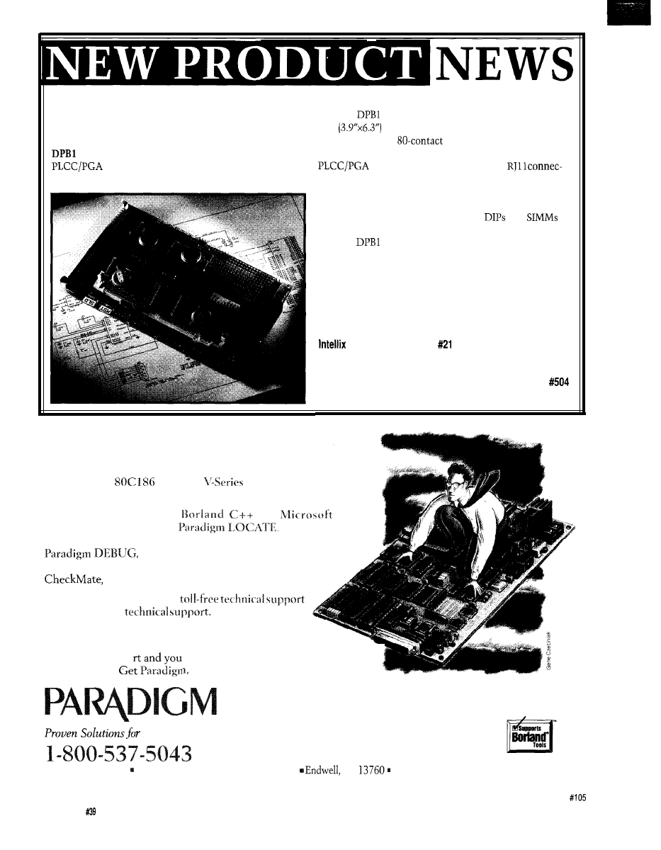
LOW-COST PROTOTYPE BOARD
The
prototype board measures 100 mm x 160
A low-cost, easy-to-use prototype board and
mm
and features three rows of SIMM
prototyping kit has been introduced by Intellix. The
patterns for up to
devices. It also provides 30
board allows 0.1” and 0.050” SIMM, DIP, and
rows of holes on a 0.1” grid for any size DIP and up to 84
devices to be easily prototyped. The kit also
devices. Patterns for DB9 and
supports Dallas Semiconductor SIPSTIK devices.
tor, and various headers are also provided.
A novel feature of the prototype board is the
staggered and straight hole patterns on 0.050” and 0.1”
centers. This allows combinations of
and
to be accommodated on the same board.
The
prototype board is also available as a
complete kit that simplifies prototyping of Dallas
microcontrollers, particularly the SIPSTIK packages.
The kit includes an RS-232 link, reset chip, reset and
serial load PLD, complete schematics, and all needed
components. The bare board sells for $39, and kit
pricing starts at $98.
l
555 South 300 East,
l
P.O. Box 526398
Salt Lake City, UT 84152-6398
(801) 534-1017
l
Fax: (801) 534-1019
No bugs on board.
Of course, what else would you expect from the acknowledged
leader in Intel
and NEC
embedded system
software development tools.
Start with the complete
and
C/C++
application templates from
Add your code and
check it out in your target system with the highly acclaimed
either stand-alone or with popular in-circuit
emulators from Intel, NEC, Applied Microsystems,
Microtek, ZAX, and others.
If you get stuck, call our
hotline for free
Then rest assured
that your embedded application is rock-solid and free
from those embedded system nasties.
After all, life is sho
can’t play hard when you’re stuck in the
lab fixing bugs.
get bug-free, and get on with your life.
Embedded C/C++ Developers
Paradigm Systems 3301 Country Club Road, Suite 2214
NY
(607) 748-5966
q
FAX: (607) 7485968
All
trademarks are property of their respective holders.
10
See us at Embedded Systems Booth # 814
Issue October 1993
The Computer Applications Journal

8032
EMBEDDED ADAPTER
microcontroller pins. This allows the designer to attach
The model ANC-3052 from
combines the
oscilloscope or logic analyzer probes to the component
best features of a prototyping adapter with the most
side of the card. The adapter pins are on 0.1” centered
commonly needed circuitry to support the Intel 8032
rows to allow use on a variety of prototype boards or, by
microcontroller. This Embedded Adapter approach
using ribbon cables, as a single-board computer. The
provides the circuit designer with a low-cost, time-saving
232 interface is accessed through either a
single
method to wire-wrap prototypes, or stand-alone systems,
in-line connector or a modular RJ-11 connector. By using
based on the 803 1 or 8032 microcontroller.
low-power surface-mount technology components, the
The adapter includes a crystal-controlled
card draws under 150
at 5 volts.
processor, 32K of on-board RAM, a
socket
As an aid to the designer in using the adapter, the
(strappable for up to 64K of user supplied PROM), and an
user’s manual includes an adhesive-backed pin
RS-232 level double-buffered serial interface which is
ing sheet to guide the wire-wrapping of the prototype
baud rate programmable up to 38.4 kbps. There are two
and a template of the adapter which the designer can use
interrupt inputs, two counter/timer inputs, and eight
as a signal-to-pin designation map. The adapter is
digital I/O lines accessible through the combination
available with either
square, 3-level
wire-wrap and ribbon cable jacks. All microcontroller
wrap pins, or gold machine pins. The ANC-3052 sells for
pins are accessible through both wire wrap and ribbon
$146.
cable connectors. A
pin auxiliary connector
Corp.
provides seven decoded
1643%
Blvd.
I/O strobes and the upper
West Los Angeles, CA
8 bits of the address lines
90024
for external circuit
(310) 473-8995
control. A power-on LED
Fax: (310)
and reset circuits are also
included on the card.
The adapter occupies
just under nine square
inches of board space and
provides wire-wrap and
test points for each of the
SOLID-STATE DISK EMULATOR BOARD
MCSI has introduced a
disk emulator board
for IBM PC (ISA) compatible computers. The
DISK IV can emulate up to three read-only or read/write
fixed or floppy disk drives with capacities ranging in size
from 32K bytes to 4M bytes, using
or
JEDEC
standard EPROMs, flash memory, and
A
program that is developed using MS-DOS, DR-DOS, or
QNX operating systems will operate without a physical
disk in a target application system.
IV can typically be configured as one
drive; two
drives; or one
drive, one
drive, and one 5
drive. In
addition,
IV will work with other physical
Micro Computer Specialists, Inc.
drives in the system.
2598-G Fortune
Vista, CA 92083
The
IV Disk Emulator Board comes
(619) 598-2177
l
Fax: (619) 598-2450
with the on-board control firmware, users manual, and
utility disk and sells for $299.
The Computer Applications Journal
Issue
October 1993
11

MONITOR FOR OR ACCESSBUS
Developers working with
or ACCESS.bus systems can now collect
bus traffic in real time with a new instrument available from Micro
Computer Control Corporation. The
101 Bus Monitor
is a stand-alone
troubleshooting tool for the
Circuit
serial bus
developed by Philips Semiconductors, and the
developed by
the
Industry Group
is a low-cost network for connecting microcontrollers and a variety
of integrated circuits. ACCESS.bus is an open industry standard for
connecting multiple input/output devices to a PC via a single port. When
connected to an
bus or ACCESS.bus network, the 101 Bus Monitor can
collect, display, or upload information on all bus activity. The battery, wall
transformer, or bus powered unit includes a display and keypad for stand-
alone operation, and a built-in RS-232 interface.
In Trace mode, the unit can collect bus messages directed to one or all
bus-device addresses. Data collection can start or stop with an external
trigger input to synchronize the unit with network events. Internal storage
can buffer up to 2700 messages. Remote operation can upload messages to a PC while collecting network traffic.
Applications include software and hardware troubleshooting, manufacturing and quality control testing, and
field service diagnostics. The 101 Bus Monitor sells for $667.
Micro Computer Control Corp.
l
Box 275
l
Hopewell, NJ 08525
l
(609) 466-1751
l
Fax: (609)
466-4116
We’re Small, We’re Powerful,
And We’re Cheaper.
In fact, you’ll get the best product for about
half the price. If you’re interested in getting the
most out of your project, put the most into it.
For the least amount of money.
Call us today for complete data sheets, CPU
options, prices and availabilitv.
Work
Welcome. Call or fax for
complete data sheets
2308
East Sixth Street
Brooking, SD 57006
Phone (605) 697-8521
Fax (605)
12
Issue
October
1993
The Computer Applications Journal
We offer a full line of low cost
embedded
controllers and software tools which are ideal for
developing products, test fixtures and prototypes.
Features Include:
Low power CMOS design
Up to 60K of code space and up to 60K of data space
5 to 15 volt operation
Small form factor (3.5”
l
6.5”) with prototyping area
System diskette includes application notes
Start at $100
Available
Options:
Multifunction Board adds
24
lines and more!
BASIC-52 or Monitor/Debugger in EPROM,
C Compiler $100 or BASIC Compiler for $300
Iota Systems, Inc.
8987
l
Incline Village, NV 89452
PH: 702-831-6302
l
FAX: 702 831-4629

NEWS
INTELLIGENT DVM
has introduced The Intelligent DVM, a digital voltmeter that interfaces to a standard IBM PC
compatible. The unit consists of a module that connects to a standard printer port and an innovative software
program that allows the user to
or convert measurements automatically. The DVM is ideal for remote
applications with a portable computer.
The Intelligent DVM possesses powerful recording capabilities. Initiation, sampling, and termination are
controlled by various combinations of time, trigger, count, and displayed value. All significant parameters may be
recorded. The software provides powerful graphing options for recorded and real-time data. Graphs may be cut and
pasted into other Windows applications, or sent directly to the printer. In addition, the software allows instant
conversion from volts to decibels, degrees
PSI, or any other user-definable scale.
Two digital outputs allow the unit to control peripheral equipment, enabling it to operate as a dedicated process
server. DVM functions are controlled externally by two digital inputs, an on-screen push button, and the DVM
displayed value. Resolution of 5% digits allows for simple interface to low-level signal sources such as thermo-
couples and pressure and strain gauges.
The Intelligent DVM autoranges from t1.2 V to
V and features an input impedance of 10
for the 1.2-V range), and a conversion rate greater than 10 conversions/second. The 3.75” x6.3” xl
unit
requires 9 VDC at 5
System requirements are a PC compatible with Microsoft Windows 3.1 and a free parallel port. The Intelligent
DVM is available in three models: The Professional Model at $329.95, the Basic Model at $289.95, and the Single
Range Model at $229.95.
4960
Expressway Suite 238
l
San Jose, CA 95118
l
(408) 997-8644 fax: (408) 997-6730
Memory mapped variables
n
In-line assembly language
option
n
Compile time switch to select
805
1 or
n
Compatible with any RAM
or ROM memory mapping
Runs up to
50 times faster than
the MCS BASIC-52 interpreter.
n
Includes Binary Technology’s
SXA51 cross-assembler
hex file
n
Extensive documentation
Tutorial included
Runs on IBM-PC/XT or
Compatible with all 8051 variants
$295.
508-369-9556
FAX 508-369-9549
q
Binary Technology, Inc.
P.O. Box 541
l
Carlisle, MA 01741
See us at
Embedded Systems
The Computer Applications Journal
Issue
October 1993
1 3

‘URES
Fire Control for
Foundry Furnaces
Stepping Up in
Performance
Data Logging Meter
are No Fluke
Fire Control
for Foundry
Furnaces
David
m a mechanical
en trying to build a
long time. My first experience contain-
ing high temperatures came sometime
in intermediate school when I discov-
ered I could power a carbon arc from
the wall plug using a salt-water
rheostat. The body of the furnace was
an old ceramic flower pot with
electrodes removed from D-cell carbon
zinc batteries. I’ve built a variety of
different furnaces and ovens since
then, each teaching new lessons
beyond finding the shortest route to
the circuit breaker. To generate heat
on a large scale, air-fuel combustion is
wonderfully cost effective, but poten-
tially dangerous. I hope to illuminate
many of the safety issues of combus-
tion monitoring and control for those
of you who might enjoy experimenting
with yet another computer peripheral
device. Please be advised that situa-
tions dangerous to life and property are
possible (probable) if you experiment
with combustion, and that the system
described in this article cannot
guarantee your safety.
OVERVIEW
The oven hosting the combustion
system has a working volume of 45
It is a steel-shelled behemoth weighing
a couple of tons. It is used to prepare
ceramic shell molds for foundry work,
and is designed to fire pottery as well.
The oven is fed by two burners, each
with its own flame monitoring system,
and its own ignition’system. The
fuel ratios are manually adjustable at
the burners, with source air and fuel
under combustion system control. The
14
Issue
October 1993
The Computer Applications Journal
oven uses forced-draft so that the
working volume is at a slight positive
pressure. Complicating burner issues,
unfortunately, the oven and the
combustion systems are outdoors,
which stresses many components
exposure to dust and rain. Addition-
ally, despite expensive insulation and
careful design, the oven provides the
potential for serious radiant and/or
conductive heat transfer to several
system elements.
The combustion control system
should provide simple, reliable, and
safe control of the oven in operation.
In my case, these goals are somewhat
constrained by concerns for time
available, cost, and ease of use.
Combustion control is normally
defined to include flame monitoring,
ignition, and control of fuel and
oxidizer mass flow rates to achieve
desired heating effects. Real-time
control of the air-fuel ratio by
ing exhaust gases for 0,, CO, or CO,
and continuous smooth throttling of
the burners are features I couldn’t
afford for this oven. I think the simple
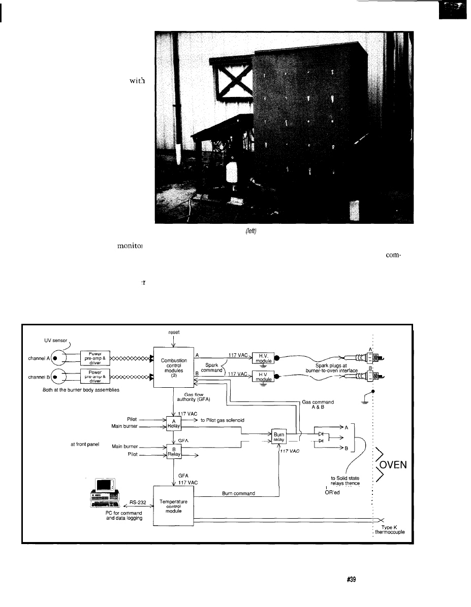
Photo l-The
combustion control system
is located next to the oven (right). Each subsystem is contained in its
own aluminum box under the top of the control panel.
ignites it when necessary. A PC
controls the temperature of the oven
by switching the burners on and off.
A high-level diagram of this
called
MO
LT E N interprets oven
mand files, communicates with the
thermocouple interface module, and
logs temperatures. Most other systems
system described in this article will
system is in Figure 1. The PC performs
are configured into two channels, one
suit the needs of most experimenters.
the management chore of deciding
for each burner; there are two flame
This system monitors the burner and
when to fire the burners. A program
sensors, two ignition systems, and a
Manual authority
and indicators on
all 4 channels
to Pilot gas solenoid
to solenoid banks.
channel for
c o m b u s t i o n
a i r o p e r a t i o n s .
Figure
l-An overview of the electrical systems for fhe oven controller. There have been several revisions over the years, creating a mixture of bought, built, and found
components.
The Computer Applications Journal
Issue
October 1993
15
Photo
air intake,
fuel supply line, and spark
plug
assembly. See Figure 3 for a labeled diagram of
the components shown here.
variety of parallel command paths
controlling gas and air flow. Typically,
where dual channels exist, they are
known as A (red) and B (blue). There
are also two pilot channels through the
control relays. The pilots were used
before the completion of the flame
control system to light the main
burners, but have since been used to
preheat molds.
points along the gas feed route. For the
main burners to have gas flow, gas
flow must be authorized from the front
of the control panel, the combustion
control system must authorize gas
flow, and the PC must request the
burners to be lit. Any of these three
controlling agents may deny the burn.
If you have enabled gas flow at the
front panel and the PC has requested
One method of conductivity
monitoring is the flame rod, which
senses current flowing in the ionized
species of the flame. This means the
rod must be in the flame. Potential
maintenance problems include fouling
normally closed in case of a power
outage. There are also manual gas
shut-off valves at a variety of choke
There are a variety of safety
heat, the flame monitoring circuitry
features incorporated into the overall
allows five seconds for a good light in
design. All gas flow solenoids are
both burners before removing gas flow
authority. This may seem lengthy, but
or drooping of the electrode and
when the oven is cold, lean air-fuel
leakage currents affecting the flame
mixtures are difficult to keep in steady
sensing decision. The flame rod is
combustion in the burners. The
ignition time-out period should be set
based on the circumstances encoun-
tered in a particular installation.
From a packaging standpoint,
most of the electronics fit into three
small aluminum boxes mounted to
the underside of the control panel.
Cables make long runs from the panel
to the flame sensors, the ignitor
modules, the thermocouple, and the
PC.
MONITORING COMBUSTION IN
THE BURNERS
Combustion detection techniques
range from simple mechanical means
to sensing flame emissions in the
electromagnetic spectrum. When
burners are sealed into a hot chamber,
techniques such as mechanical or
based thermostats, thermocouples, and
temperature sensing IR pyrometers
can’t readily be used. That leaves
detecting combustion by monitoring
changes in conductivity, emissions in
and around the visible spectrum, and
acoustic signature.
Figure
size, and weathering were primary concerns for the defection
burners.
support electronics info small PVC plumbing
fixtures which attach base of
housing mounted in burner.
16
Issue
October 1993
The Computer Applications Journal

Oven
Hot
Face
20,304 SS, 6 Places
1
Tee With
1
Gate Valve
PVC Reducing
azed Fuel Feed
e (Drilled Orifices)
Union
Polypropylene Hose Fitting
lit Clamped
SS Hose Clamp
UV Sensor In Phenolic Housing.
Sensor Field Of View Set Above
or Below Fuel Feed Pipe
Airflow ---
Figure
detector assembly slips info the
just ahead of the propane feed. Alignment is performed by adjusting the detector assembly while looking down fhe
burner bore from inside the oven.
simple technology, but I prefer to put
that look at the AC component (less
system components outside the raging
than
1
of the radiation to detect
inferno for longevity.
the chaotic flame front. These systems
While acoustic monitoring seems
are sometimes used while burning
an intriguing possibility, I decided to
materials which are strongly
build a system based on technology
let absorbing, such as hydrogen sulfide.
the industrial sector uses everyday. For
For simplicity, it is hard to beat
noncontact combustion monitoring,
monitoring the ultraviolet spectral
systems typically use infrared
emissions of combustion.
sions and/or ultraviolet emissions. For
You can go out and buy “purple
hot chambers, there are IR systems
peepers” and hook them to flame
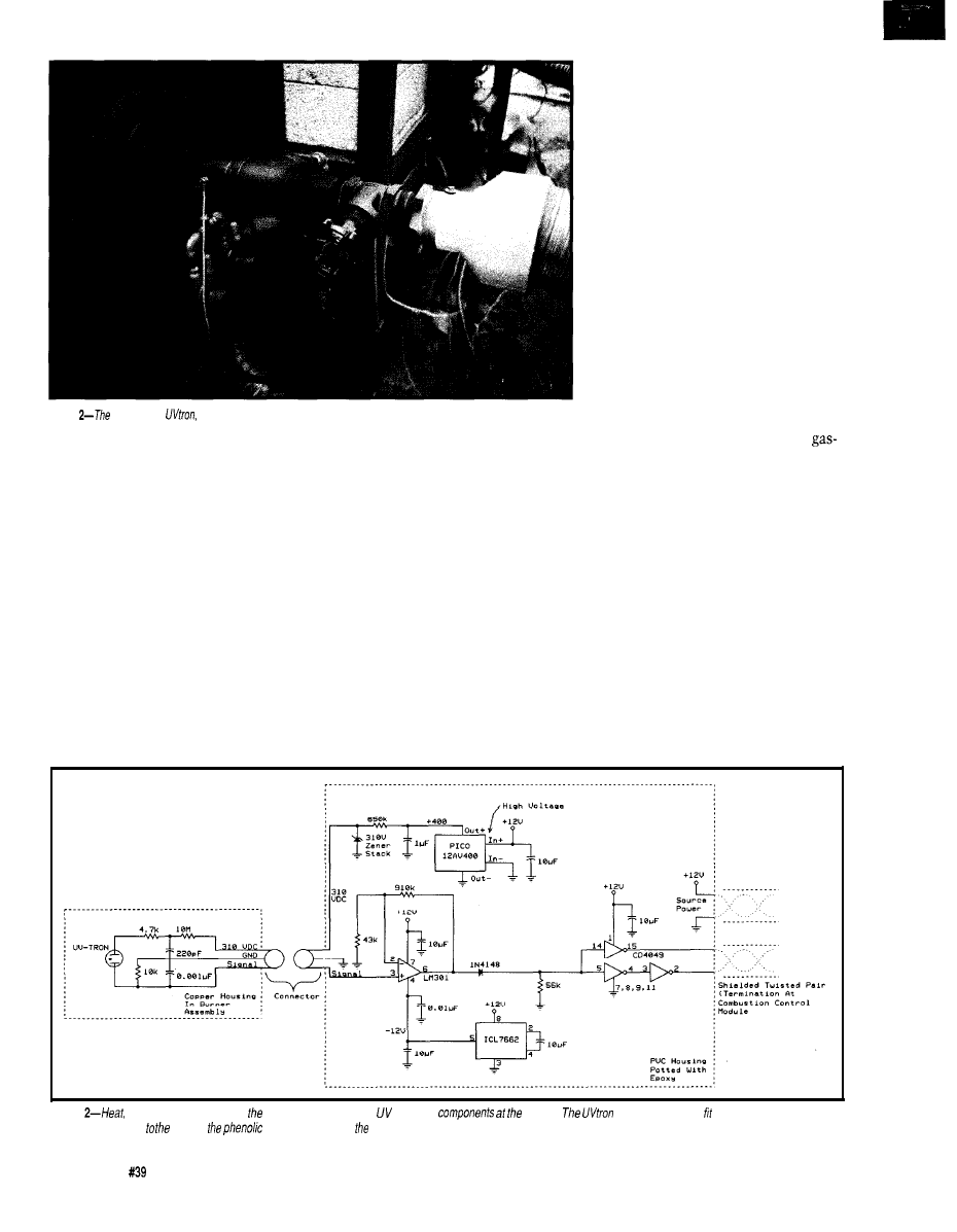
Figure
4-The
performs
as a differential amp and comparator for the incoming pulse train from fhe
signals subject to solenoid spikes were isolated as necessary.
managers for a couple of kilobucks,
but where’s the fun in that? Solar blind
UV detectors are relatively cheap at
$35, and are easy to work with. While
there are some solid-state detectors
out there, the large installed base of
products surrounds the gas discharge
tube. The careful choice of spectral
response of the tubes makes them
sensitive to
flame emissions, but
unable to detect solar illumination,
most domestic light sources, or the
black body type emissions of a very
hot oven. I chose the Hamamatsu
tube for this project, a tube they
describe as a
It is sensitive
from 185 to 260 nm and is small
enough to get into the tight spaces of
my burner assembly.
In use, the tube has a 300350-volt
potential across it. The photoelectric
effect causes the cathode to emit
electrons when the incident photons
have enough energy to excite them off
the surface. After the electrons are
emitted from the cathode, they
accelerate in the electric field toward
the anode. They excite some of the
low pressure gas molecules they find
along the way, creating ions and more
electrons. The ionized pathway in the
tube created by this avalanche con-
ducts nicely, with the current flow
signifying that UV radiation has been
The Computer Applications Journal
Issue
October 1993
17

Command
Command
Gas Command
Command
Figure 5-This timeout
circuitry features an annoying alarm
the user when Gas
has been revoked. The most
problem invoking this circuitry
involved a
fuel regulator frozen solid with ice in 95” heat
detected. The tube is not self-quench-
ing, so the driver circuitry must reduce
the voltage across the tube after
discharge starts until discharge has
ceased. This is simply done with an
RC network as shown in Figure 2. The
capacitor defines the limit of
the total energy available to the
discharge process so damage to the
tube does not occur. The specifications
for the
recommend an average
discharge current of only 100
max.). Under operating conditions,
the circuit shown generates a pulse
train between 0.5 and 1 volt in
amplitude, which is then available for
further processing.
Coming up with power for the
UVtron isn’t as difficult as it might
seem at first. You need tenths of a
milliamp between 300 and 350 volts
for the
I found that the flash
units in disposable 35mm cameras
generate 325 volts. The units store that
used in the current design are set to
voltage in a capacitor until discharge
detect a lighter at about five feet. At
time. The supply had no trouble with
five feet, the tube is very actively
the
current requirements.
discharging with a slight purple light.
also built a voltage quadrupler from
Note that tubes should not be allowed
120 VAC using diodes and capacitors
to see each other discharging as the
in the standard ladder configuration.
event is UV rich. The best source of
This system, with filtering and zener
in the flame is the root area at the
regulation, also works well. A variety
burner’s mouth. The UVtron can be
of companies also sell small pulse
looking coaxial to the burner boresite,
transformers which could be used to
or looking obliquely at the burner
construct a high-voltage supply.
entry point into the oven. In my
chose to use the microminiature Rico
system, I chose to mount the UVtron
high-voltage supply. It was
within the burner airstream. This
encapsulated and had plenty of reserve
reduces the number of oven hot face
capacity.
penetrations.
The UVtron is quite sensitive.
Hamamatsu claims the R2868 can
detect a lighter’s flame from over
sixteen feet. My own testing shows
that discharge events were triggered by
such a flame from a broad area in the
small workroom I use. The thresholds
The pulse-forming circuitry and
the UVtron fit into a slender phenolic
tube which slides into the burner
assembly as shown in Figure 3. The
UVtron looks down the bore into the
oven. Previous mounting configura-
tions used copper tubing, with
G a s F l o w A u t h o r i t y
AC Power
N o t e :
It
D C : 1 0 - 3 0 U
17
UDC
Solid-Stats
2 4 0
provisions for forced-air cooling.
I
discovered that I didn’t need the
internal cooling, and the metal contact
with the ignition circuitry was causing
unusual behavior from the signal
conditioning circuitry. I found the
phenolic tubing ideal since it is easy to
work with and is a good insulator.
Cooling is now externally supplied
by fans when the burner is off, and is
supplied by the feed air when the
burner is on. The base of the phenolic
tube connects to a small PVC housing
which contains
support
electronics. Within the small housing
is a
miniature 400-volt power
supply, an amplifier, and the CD4049
inverter, which I used as a “differential
line driver” to minimize data artifacts.
Each of the four devices in the housing
was wired separately (no circuit board)
with very close component placement.
After successful testing, many layers
of clear nail polish were applied to
each circuit assembly. The insulated
pieces were then stuffed into ex-
tremely tight quarters with the feed
cable and epoxy filled to seal out
mother nature. The feed cables to both
flame sensors are about twenty feet in
length. The cables run to the control
panel through occasional mud.
If you haven’t guessed by now, the
electrical environment is very noisy.
There are nine solenoids clacking,
three big cycling motors, a pair of
spark plugs, and a sad host of 60-Hz
cabling everywhere. The first-genera-
tion system suffered some noise
problems due to poor attention to
proper grounding and shielding
termination techniques. The current
design has proven successful in the
harsh environment.
The cables running back from the
UV sensors have two shielded twisted
pairs of 22 AWG wire. The shields are
terminated at the signal conditioning
circuitry. One pair runs 12 volts to the
sensor package, while the other
returns the
square wave pulses
from the tube. Figure 4 shows the
integration processing of the pulses.
I
used an LM392 for the convenience of
having an op-amp and a comparator in
a single
DIP package. With my
cabling and termination, the gates
were delivering a clean 6-volt signal at
the resistive load. [While this is
entirely adequate for this application,
longer cable runs would probably
demand a “real” line driver and
receiver.)
The rest of the circuit integrates
and thresholds to provide a Boolean
flame signal.Ignition is required when
the output of the comparator is high.
The time constants used in the
integrator are not critical. The signal
ramps up quickly and decays within a
half second with the values shown.
The values chosen for your application
could vary, depending on the stability
of the burners, for instance. Make sure
the
can’t see the spark plug
gap or the system might oscillate on
and off even though the gas isn’t
burning! Sparks generate UV.
Figure 4 also shows input isolation
from the console. The DC used in
much of the control panel operations
is 19 volts. This voltage was mandated
by a box full of surplus gas solenoids,
but it is also conveniently compatible
with the solid-state relays. Front panel
commands are converted to 12 volts
through the isolator and fed to the
simple time-out logic shown in Figure
5. The signal shown as Gas Command
is the front panel switch
with
the PC burn request signal using a
mechanical relay.
When gas flow is requested at
either burner, and there is no UV
detected at the burner, then the
system has roughly five seconds to
establish steady combustion. After
that time, the signal Gas Flow Author-
ity is removed by the CD4013 flip-flop,
and an obnoxious alarm goes off. The
signals Gas Flow Authority, Spark
Drive A, and Spark Drive B run out to
the power supply box, where all 60-Hz
operations are performed. Three small,
solid-state relays switch the AC to
drive 120-VAC drop-out relays and the
solid-state ignitors. The signal process-
ing box has no AC power or signals in
it.
IGNITING THE BURNERS
The burners are lit with standard
spark plugs. I threaded steel pipe and
welded into the 1 S-inch burner tube.
The spark plug cavity sits very close to
the back wall of the oven. It should be
INTERFACE
RELAY INTERFACE. . . . . . . . . . . . . . . . . . . . . . .
relay
ports are
for
to 16
(expandable to 128
cards).
relay
port connects to a
wd or
block. A variety of relay cards and
slays are stocked. Call for more info. RS-422 available
to
PS-4 port selector ma
control
AR-16
(up to 16,
be used
4
REED RELAY CARD (8 relays, 10 VA) . . .
RELAY CARD
6 RELAY EXPA
277 VAC)
CARD (16
D I G I T A L
( C
O N N E
CTS TO
CONVERTER
channel, 8
temperature.
amperage,
sage, energy demand,
levels,
movement and
wide variety of other
of analog signals.
may
e ex
ST-32 expansion cards. 112 relays may
to 32 analog or 126
using the
using
6 expansion cards.
be configured for temperature input using
i
e
AS-422
may be used to conned satellite ADC-16
(up to 4,096 analog
6,364 status
relays). Call for info on 10 8 12 bit converters.
Mock and
sold separately]
STATUS EXPANSION CARD . . . . . . . . . . . . .
Put
status of relays, switches, HVAC equipment.
smoke detectors and other
keypads and binary coded
32 status
(opt0
separately).
E-8 TEMPERATURE INPUT CONVERSION .
$49.95
8 temperature sensors terminal
ran is minus 40 to 145 degrees F.
PORT
(4
an RS-232
.
79 95
OUCH TONE
and other serial interfacing
into 4 selectable
available. Cdl for free information packet.
FULL
over the
F R
one by our staff. EACH ORDER INCLUDES A
E
DISK
PRO
G R
A M M I N
G
E
X
A M P L
ES
I N
BASIC, C AND ASSEMBLY LANGUAGE. A detailed
technical reference manual also
for continuous24
hour industrial applications.
socketed.
Use with IBM and
Tandy, A
most other computers
or
Mac and
ports.
All standard baud rates and protocols may be used
to 19.200 baud).
International Domestic FAX (614)
Use
technical
orders
ELECTRONIC ENERGY CONTROL,
INC
.
South Fifth Street,
604
Columbus. Ohio 43215
The Computer Applications Journal
Issue
October 1993
19

“upwind” but reasonably close to
where you find the flame attachment
point to be on your burner. I used a
ignitor module to fire
the plugs. It has a standard automotive
plug fitting, is completely encapsu-
lated, and isolated from the line
voltage. I went to a performance
automotive store and had a pair of
eight-foot cables made with spark-plug
fittings on both ends. These are
temperature, solid-conductor cables
that were expensive, but worth it.
They sit in the mud and still perform.
Standard feed wire for a neon sign is
good for experimentation, but would
require a relatively cool installation for
longevity.
The ignitor modules are screwed
to a bracket which is mounted to the
heavy steel of the chimney frame,
which in turn is bolted to the frame of
the oven. The ignition current from
the ignitors runs through the burner
assembly into the shell of the oven,
where it eventually finds the chimney.
In my zeal to reduce noise during early
experiments,
I
chose to provide a very
1020
1 0 1 0
1 0 0 0
9 9 0
9 8 0
9 7 0
9 6 0
9 5 0
9 4 0
Control Cycling at 1000 F
15
Loop 2
0
5
1 0
1 5
20
25
Time (min)
Figure
cycling for fifteen minutes at 1000°F overshoots the intended target.
clean
return path for the ignitors. The
nothing else, the oven is better
chimney, the oven frame, both
prepared for lightning. The ignition
burners, and the ignitor bracket were
wires broadcast quite a bit of noise,
tied together with
copper
and should be as short as possible.
wire. These lines join at a common
Most commercial flame control
point, which is a six-foot copper
literature describes similar remedies
grounding rod sunk behind the oven. If
for noise interference and grounding
1 2 Year Warranty
l
Support by phone
l
30 day Money Back Guarantee
l
FREE software upgrades available via BBS
l
Demo SW via BBS
2716 8
16 bit
l
Flash
(EMP-20 only))
l
Micros
42A. 42AH.
49H.
NEEDHAM'S
4539 Orange Grove Ave.
Sacramento, CA 95841
am-5 pm PST)
C.O.D.
BBS (916) 972-8042
FAX
972-9960
Issue
October 1993
The Computer Applications Journal
problems. Proper shielding and
grounding practices must be observed.
DECIDING WHEN TO BURN
The last box under the control
panel is the temperature control
module. It contains two I/O modules:
one 120-VAC input and one 120-VAC
output. The I/O modules support a
small microprocessor-based thermo-
couple interface device made by DGH.
The DGH D1321 is a small (fits in
your palm) general-purpose module
designed to support process control.
This particular module uses RS-232 for
communication and reads type-K
thermocouples. It also has a couple of
input and output lines, and could
actually have performed a temperature
controller function in a stand-alone
mode. I chose to use it only as a
remote I/O device for my PC.
The PC is located in a nearby
building that is air conditioned. The
temperature control box and the PC
are linked with a
RS-232 link,
running at 9600 bps. At one point in
the development, I considered building
up the remote I/O capability from one
of the many single board computer
options. I opted for immediate satisfac-
tion and bought the D1321.
The temperature control module
reads the Gas Flow Authority line
through the 120-VAC input module
(see Figure 6). A
signal is sent to
the D1321 as long as the flame
monitoring circuitry believes safe
conditions exist at the burners. At PC
instruction, the D1321 issues the Burn
Command, which is translated to
VAC and output for relay use.
The D1321 also reads the
gauge, type-K thermocouple embedded
in the wall of the oven whenever the
PC requests the read. The bead of the
thermocouple just extends into the
oven volume, with a fine layer of
bonding it to, the oven wall.
This helps to protect the thermo-
couple, but at lower temperatures, it
also keeps the system from rapid
cycling. Rapid cycling occurs when the
thermocouple is responding to the hot
combustion gases and not the actual
oven hot-face temperature.
The fire coupling to the thermal
mass of the wall essentially low-pass
Control Cycling at 1600 F
1 6 2 0 ,
15
10 Loop 5
1 5 6 0
1 5 5 0
I
I
I
I
I
I
I
0 2 4 6 8 10 12 14
16
Time (min)
Figure
cycling for fifteen minutes at
results in a slower moving, easier to control oven
temperature.
filters the temperature data. Some of
can perform well, and the price is
you may be able to afford an alumina
right.
ceramic sheath for the thermocouple.
A note about thermocouples. If
This would perform some filtering in
you plan to have unusual combustion
addition to providing an ideal
atmospheres at very high temperatures
ment for the long-term survival of the
(corrosive or strong oxidation), you
thermocouple. Careful placement of
should have a few spare
the thermocouple and a little
couples. It is difficult to make your
Real- Time Multitasking with DOS
for Microsoft C, Borland C, Borland/Turbo Pascal
Develop Real-Time Multitasking Applications under MS-DOSwith
RTKernel is a professional. high-performance real-time multitasking kernel. It runs under MS-DOS and supports
Microsoft C, Borland Ctt. Borland/Turbo Pascal, and Stony Brook
RTKernel
you can link to your
It lets you run several C functions or Pascal procedures
tasks. RTKernel offers the following
advanced features:
event-:
Hostess boards)
performanceislndependentofthenumberoftasks
can
OR-DOS.
1
measurement (1
Interrupt handlers
*perform
tasks
re-entrance problems
Inter-taskcommunicatlonsusingsemaphores,
message-passing
usable by other tasks
Interrupt handlersforkeyboard. COM
no run-time royalties
1.012.013.x).
$ 4 9 5
$445
Mastercard,
check. banktransfer, COD accepted
32
Homburg
Professional Programming
Tools
Phone
74 72
43
The Computer Applications Journal
issue
October 1993
2 1
own heavy-gauge thermocouples, but
companies like Omega Engineering
sell them affordably. For applications
which do not require temperatures
close to the melting point of the
thermocouple, you would do well to
buy a good-sized spool of the
gauge pair. Type-K thermocouples
with the woven ceramic insulation
should suffice for most experiments.
The beads can be made with any
acetylene torch, or you may spot weld
them with a big capacitor.
The program MOLTEN runs on the
PC to coordinate the whole oven
control problem. MO LT E N reads in
command files and attempts to make
the oven perform as directed. It
monitors, but does not command, the
flame maintenance operations. The
program requests burns to be per-
formed, and monitors temperature
inside the oven. It uses the DGH
module as an intelligent peripheral in
a harsh remote location. MO LT E N was
written in C to provide the control
needs of the oven, meaning that it does
not have a slick user interface. MO LT E N
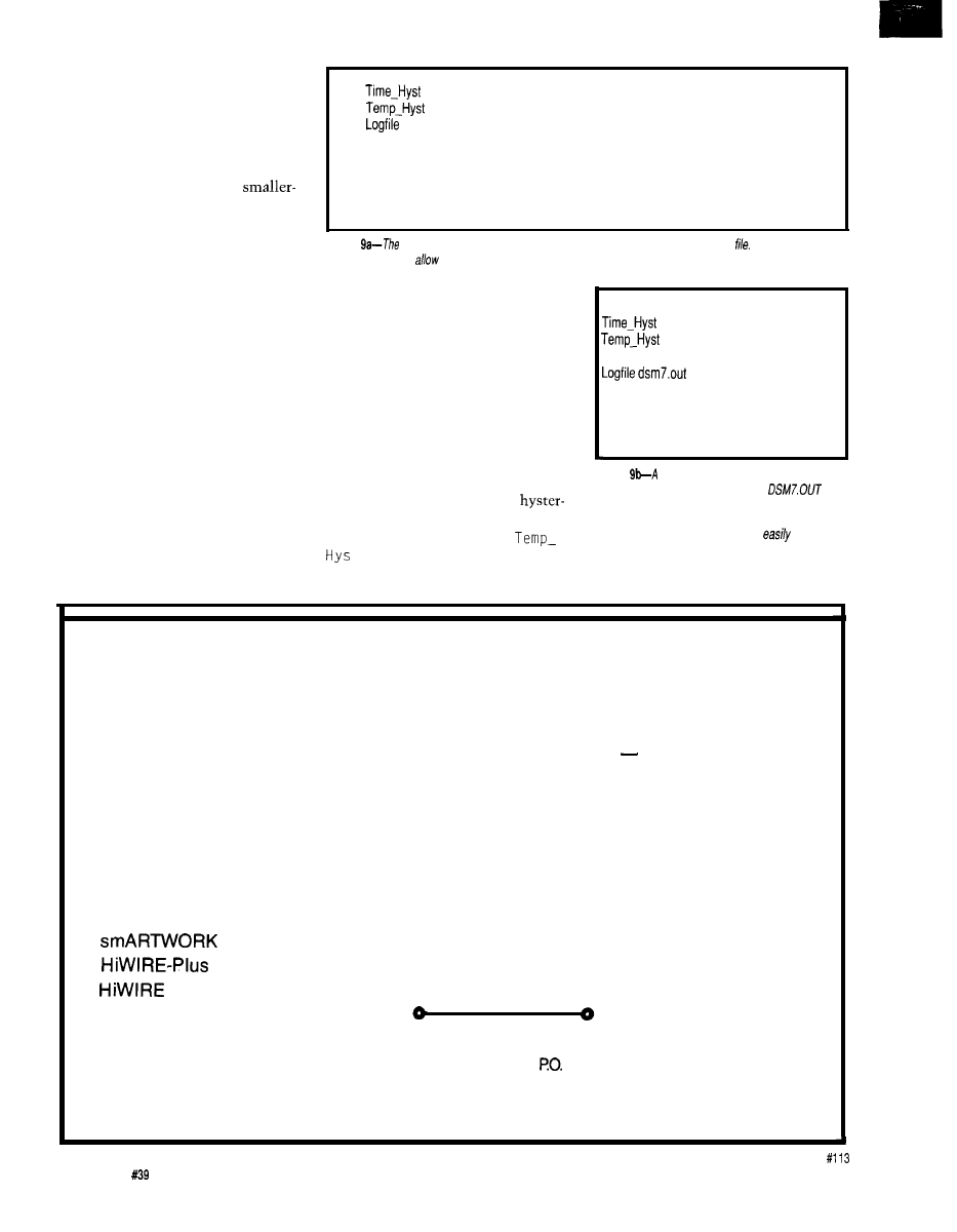
LogLoopTime
Wait
Enable
Soak
Disable
num
(seconds)
num
(degrees F)
filename
(file put in local directory)
num
(seconds between data samples)
num
(minutes, log active)
(burner use authorized)
numl
num2
(numl = temp F, num2 = minutes of soak)
(burner use no longer authorized)
Figure
MOLTEN control program reads ifs commands from a prepared command The program
supports enough to
intelligent control of the burners
uses the interrupt-driven serial
communications routines supplied by
* this is a command input file for MOLTEN.EXE
DGH with their software and samples
15
disk. The software is otherwise
10
without complexity.
LogLoopTime 5
The control scheme I chose for
Enable
this first-generation MO LT E N is often
Soak 1600 120
referred to as bang-bang control. The
Disable
state of the system (on or off) is
Wait 180
mandated by system position relative
to two limits. Most home ovens work
Figure
MOLTEN
command file used to generate
this way, cycling between the
oven cooling curves is shown. The file
would contain a header of useful information followed
esis boundaries around some chosen
control point. The command
t
is used to define the acceptable
by two columns of data containing time in seconds and
temperature at that time. This data is
imported
into spreadsheet programs for analysis.
hysteresis for the system.
MANUFACTURERS OF PROTOTYPE PRINTED CIRCUITS FROM YOUR CAD DESIGNS
TURN AROUND TIMES AVAILABLE FROM 24 HRS
2 WEEKS
Special Support For:
l
TANGO.PCB
l
FULL TIME MODEM
l
TANGO SERIES II
l
GERBER PHOTO PLOTTING
l
TANGO PLUS
l
PROTEL AUTOTRAX
WE CAN NOW WORK FROM
l
PROTEL EASYTRAX
YOUR EXISTING ARTWORK BY
l
SCANNING. CALL FOR
DETAILS!
l
l
II
l
EE DESIGNER I
Express
l
EE DESIGNER III
l
ALL GERBER FORMATS
Circuits
Q u o t e s :
1150 Foster Street
l
Box 58
l - 8 0 0 - 4 2 6 - 5 3 9 6
Industrial Park Road
Phone: (919) 667-2100
W i l k e s b o r o , N C 2 8 6 9 7
Fax: (919) 667-0487
EXPRESS CIRCUITS
2 2
Issue
October 1993
The Computer
Applications Journal
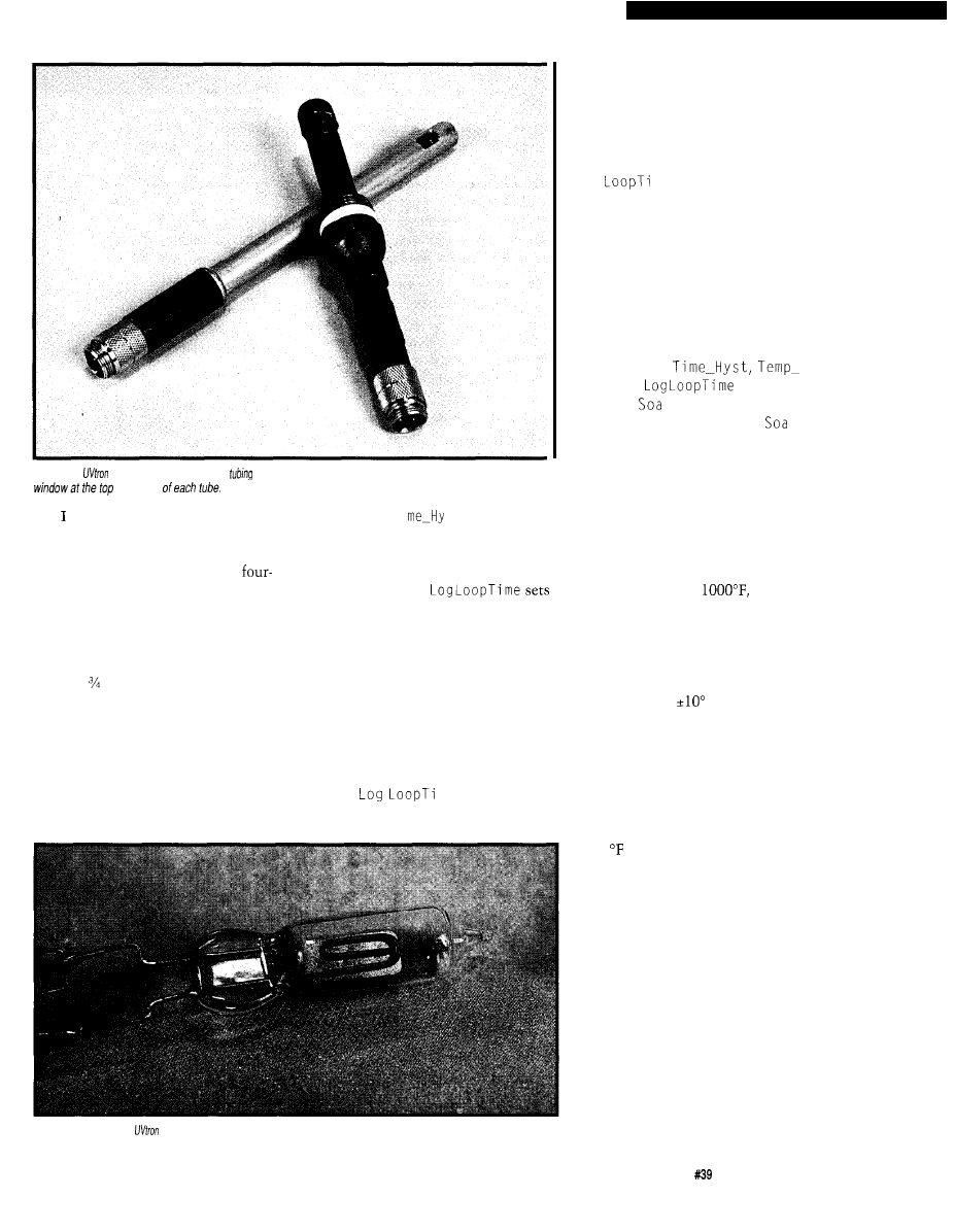
Photo 3-The
sensor is built info pieces
of
to ease its
installation.
The sensor actually
peeks out the
have the additional constraint
that the system can’t be quickly
cycled. There is a substantial fraction
of a second required to open the
inch butterfly valve which provides
the feed air to the burners. An artifact
of this slight delay is a rich mixture for
lighting, which is beneficial. It takes
even longer for the valve to close,
perhaps second. The delay results
from the large pneumatic actuator the
valve uses, and is not unreasonable.
What this means, though, is that I
really can’t cycle the burners on and
off at a high rate of speed. There is also
wear and tear to be considered. To
account for mechanical limitations,
the command
T i
s t
(temporal
hysteresis) gives the system a grace
period after a transition from either
state.
Thecommand
the
time
period to elapse between
temperature samples in seconds. Each
time the D1321 is called, the state of
Gas Flow Authority is reported, and
the temperature is reported. There is
also error checking during reporting:
MOLTEN
and the D1321 processor
check command and response mes-
sages against generated checksum
bytes appended to messages. Presum-
ably, the
me
could be set to
fractional values for sampling several
Photo 4-A closeup of
the
shows its construction.
times a second, but my system doesn’t
need that kind of data bandwidth, and
the log files get huge.
If a log file has been declared, the
commands
W a i t
and So a k will
generate new data for the log file at the
Log
me
interval. Otherwise, the
time and temperature will only be
logged to the screen. The command
W a i t
is specifically for taking data,
letting the oven coast while logging
temperature.
The So a k command actually
forces the oven into action. It is a
time-based loop that uses the PC
internal clock to gate its actions. The
valuesgivento
Hyst
and
controlthe
actions of
k. Examine Figures 7
and 8 to see the results of the
k
command on the oven. Both plots
show fifteen-minute burn schedules
around a target temperature.
From examining the two charts, it
is apparent that the slopes of attack
and decay are different for different
temperatures. The higher the slope,
the more the overshoot in this simple
control scheme. At
the
overshoot can be almost 10” beyond
the hysteresis band. At higher tem-
peratures, the oven temperature moves
slowly and is easier to control.
My applications don’t require
accuracies near
of a target
temperature, but I’m pleased the
system is that nimble. For ceramic
shells, I work in the 1600-1900” range
where that kind of tolerance can easily
be maintained. I have not yet fired
pottery in the oven, but at a cone 10
firing temperature (from 2345 to
238 1 depending on heating rate), the
oven should be very cooperative (slow)
to control.
A complete list of the commands
that are currently processed from the
input file are shown in Figure 9a.
Numeric arguments are of type
I NT.
Figure 9b shows a typical command
batch file. Lines are parsed into tokens
separated by white space. If the first
token in a line is a known command,
the line is interpreted. Otherwise the
line is a comment line. It requests two
hours at 1600°F followed by three
hours of data logging. Data is taken
every five seconds.
The Computer Applications Journal
Issue
October 1993
2 3
ADDITIONAL THOUGHTS
There is one safety feature I
should add. In retrospect, it would be
good to monitor the spark command
line at pin 1 on the LM392 amps. Both
lines could be inverted and
and
fed to the remaining input on the
D1321. In this way, testing of the
could be performed occasion-
ally. One of the failure modes of the
is constant discharge. When-
ever the burn command is removed,
the spark command lines should show
no combustion. This would also test
some relays in the system. Some
commercial systems have a
checking feature which, is a shutter
that covers the tube at a regular
interval. The processing circuitry then
expects to see a regular pattern of
notched data from the tube.
large in the oven would warrant
controlled ramping to reduce the
chances for cracking. While it might
be fun, probably won’t add
tuning PID control algorithms to
MO LT E N since the current temperature
control scheme meets my needs. This
project has switched from something
to improve into something to use. My
first bronze castings were poured last
spring,
I
intend to make more.
q
David
spent seven years in
the Machine Perception Section of the
Robotics and Automation Department
at the Southwest Research Institute.
He
pursues other interests
including alternative energy and
sculpting.
I will probably add a Ramp
Software for this article is avail-
command to the available commands
able from the Circuit Cellar BBS
in MOLTEN
at
some point in the future.
and on Software On Disk for this
That would allow controlled gross
issue. Please see the end of
temperature changes, which is cur-
in this issue for
rently only possible by taking steps
downloading and ordering infor-
with the
k command. Something
mation.
Omega Engineering, Inc.
P.O. Box 4047
Stamford, CT 06907-0047
(203) 359-1660
Fax: (203) 359-7807
DGH Corp.
Box 5638
Manchester, NH 03 108
(603) 622-0452
Fax: (603) 622-0487
Hamamatsu Corp.
P.O. Box 6910
360 Foothill Rd.
Bridgewater, NJ 08807
(201)
Fax: (201) 231-1218
401
Very Useful
402 Moderately Useful
403 Not Useful
SPECIAL SUBSCRIBER OFFER
GPZS Audio Sampling System
Wiring Your House for the 21st Century
Multiprocessor Architecture using DSP
VISA,
or International Postal Money
Order (U.S. funds drawn on U.S. bank only)
Circuit Cellar
File
‘includes domestic delivery. Please add $2 for
add $4 for other
The
ROM
emulation technology:
Mbit
includes a day,
no-risk money back guarantee!
Call Today 8 0 0 - 7 7 6 - 6 4 2 3
Grammar
Engine
Inc.
921
Dr., Suite 122
Westerville, OH 43081
Fax
See us at Embedded
Booth
2 4
Issue
October 1993
The Computer Applications Journal

Tom Dahlin
Stepping Up in Performance
Driving High-power
Stepper Motors
have been treated to
several articles over the years on
stepper motor applications and drive
circuits. In all cases to date, the
stepper motors used in those articles
were of the low-current type, which I
will characterize as requiring under
1
amp per motor coil. Several
exist
which are capable of directly control-
ling motors in this class, the most
common being the UCN5804 from
Allegro Microsystems. Such devices
make interfacing a microprocessor to
stepper motors a snap, conserve board
space, and generally make life easier
for the system designer.
You may find it helpful to dig out
and review material on stepper motor
construction (see references), bipolar
and unipolar drives, and step formats.
To save space here, I’m going to
assume you have that stuff down pat.
What do you do when the need
arises for a motor that requires more
current than can be provided by the
Stepper motors are avail-
able in torque ratings of over 500
pounds, making it possible to easily
control some really neat (albeit
bordering on scary] stuff. For instance,
think of a computer-controlled X/Y
table with a wood router as a pen. The
only thing separating your computer
from those heavy-duty applications is
a method of driving the larger motors.
In this article, will discuss drive
circuits that are appropriate for
medium to large motors requiring
from one to four amps of current. I will
start by adding a power-boosting stage
to the UCN5804. I will then contrast
that circuit with a more efficient
chopper type. Finally, will conclude
by showing some low-chip-count
implementations of chopper-based
stepper motor drive circuits.
MOTOR RATINGS AND SIZES
Manufacturers of stepper motors
usually group them by size. It is com-
mon to find motors listed as
size 17,
and so forth. NEMA
refers to the National Electric Manu-
factures Association which has [among
other things) standardized the base
dimensions for motor cases and
mounting hardware. You can get a
feeling for the size of the base by divid-
ing the NEMA code by
10.
For in-
stance, a NEMA 34 motor has a base of
roughly 3.4 inches on a side. Table 1
shows a rough guide to what is avail-
able and the cost on the surplus mar-
ket.
DRIVER TYPES
The two most popular methods for
providing current to stepper motors are
L/R [pronounced “L over R”) and
chopper drivers. Each of these drive
methods can be used in a unipolar or
bipolar configuration, but most L/R
drivers tend to use a unipolar drive
while the chopper types most often
use a bipolar drive.
N E M A
Base Size
1.65
2 3
2.22
3 4
3.27
4 2
4.20
Torque Range
(oz.-in.)
1 5 - 3 0
40-l 50
1 5 0 - 3 0 0
500-l 300
Current Range
0.2-i
0 . 2 - 4 . 0
2-l 0
Price
2
$1
Table l--The
Manufacturers Association
lists
motors available in today’s market.
26
Issue
October 1993
The Computer Applications Journal

R e s i s t o r
( 4 X M o t o r C o i l R e s i s t a n c e )
D r i v e
D r i v e
You may also have heard the term
resistance (ohms]. As shown in Figure
“microstepping” driver. This is a
technique used to produce many
intermediate steps between the
motor’s natural steps. Remember how
we can produce a half step position in
the motor by turning on both coils at
the same time? A microstep driver
carries this principle further by using
two
to produce sine and cosine
drive waveforms to the motor instead
of on/off step pulses. Current control
is usually accomplished using a
chopping technique for microstep
drives, but I won’t get into that
technique here.
DRIVE
The L/R method uses the motor’s
internal resistance, sometimes in
conjunction with an external series
resistor, to limit the current through
the motor’s coils. It is most often used
to drive small stepper motors using a
unipolar drive. The series resistance of
the circuit limits the current flow to
prevent the motor coil from burning
up. This circuit is shown in Figure la.
To overcome the limitation
caused by the LR time constant, we
can increase the resistance of the
circuit by using an external series
resistor
and increase the voltage
applied across the series pair as shown
in Figure lb. The value of the series
resistor is typically chosen to be two
to four times more than the motor’s
internal resistance. In an
driver,
the series resistor is four times the
internal resistance of the motor and
the applied voltage is increased to five
times the motor’s rated value. This has
the effect of reducing the time con-
stant by a factor of four, thus allowing
faster step rates. The tradeoff is that
Figure 3 shows a circuit that adds
a power booster stage to the
5804. This is done by using four
Darlington transistors. While having
the advantage of being easy to under-
stand, it requires good construction
and power wiring techniques. is
particularly important to place the
protection diodes near the Darlingtons
and to provide a good, low-inductance
current path for the Darlington
emitters. Pay attention to the power
dissipation of the series resistors,
These are best mounted directly on a
chassis, rather than on a circuit board.
My breadboard of this circuit is shown
in Photo 1.
CHOPPER DRIVES
Chopper drives offer an improve-
ment in efficiency and speed perfor-
mance as compared to L/R drivers. A
basic chopper drive is illustrated in
Figure 4. Here, a supply voltage is used
The L/R method starts to present
the series resistor is using up most of
that is five times that of the motor’s
problems as more performance is
the power going into the circuit.
rating. If the power transistor were
demanded from the motor. The two
Consider that a
series resistor
turned on and left on, the current
main problems are loss of torque at
high speeds and poor power efficiency.
Let’s address the first issue. The
loss of torque is due to the current
rise/fall time limiting effect caused by
Ideal Waveform
the inductance
in the motor coils. The
current in an LR series circuit requires
about five time constants to reach a
steady state once an impulse (i.e., a
step) is presented and another five
time constants to decay back to zero
Limited Waveform
when the impulse is removed. This
time constant (in seconds) is calcu-
lated as the motor’s coil inductance (in
henrys) divided by the circuit’s series
Figure 2-M
time constant limits rise/fall times. Average current available to the motor coils decreases as the
stepping frequency increases.
2, at low speeds [less than 100 steps
per second) the LR time constant is
usually not an appreciable amount of
the duty cycle. But as the step rate is
increased, we eventually reach a point
where the current has not yet reached
a steady-state maximum before the
drive current is switched off. In the
Figure 1-a) In a simple
driver, the
source,
is chosen to be equal to the motor’s rated operating
voltage, and the current is limited by the coil resistance.
Adding an external series resistor shortens the
time
constant of the circuit and improves performance at
higher stepping speeds. an
scheme, the
series resistor is four times the resistance of the motor
coil,
and the supply voltage is increased to five times
the motor’s rated value. Note that of the drive power
is going into resistor when this scheme is used.
with 3 amps going through it will
dissipate 90 watts! Better not touch
that little radiator with your bare
hands.
A HIGH-POWER
EXAMPLE
same way, the current cannot decay to
zero before the next step is applied.
The Computer Applications Journal
Issue
October 1993
2 7
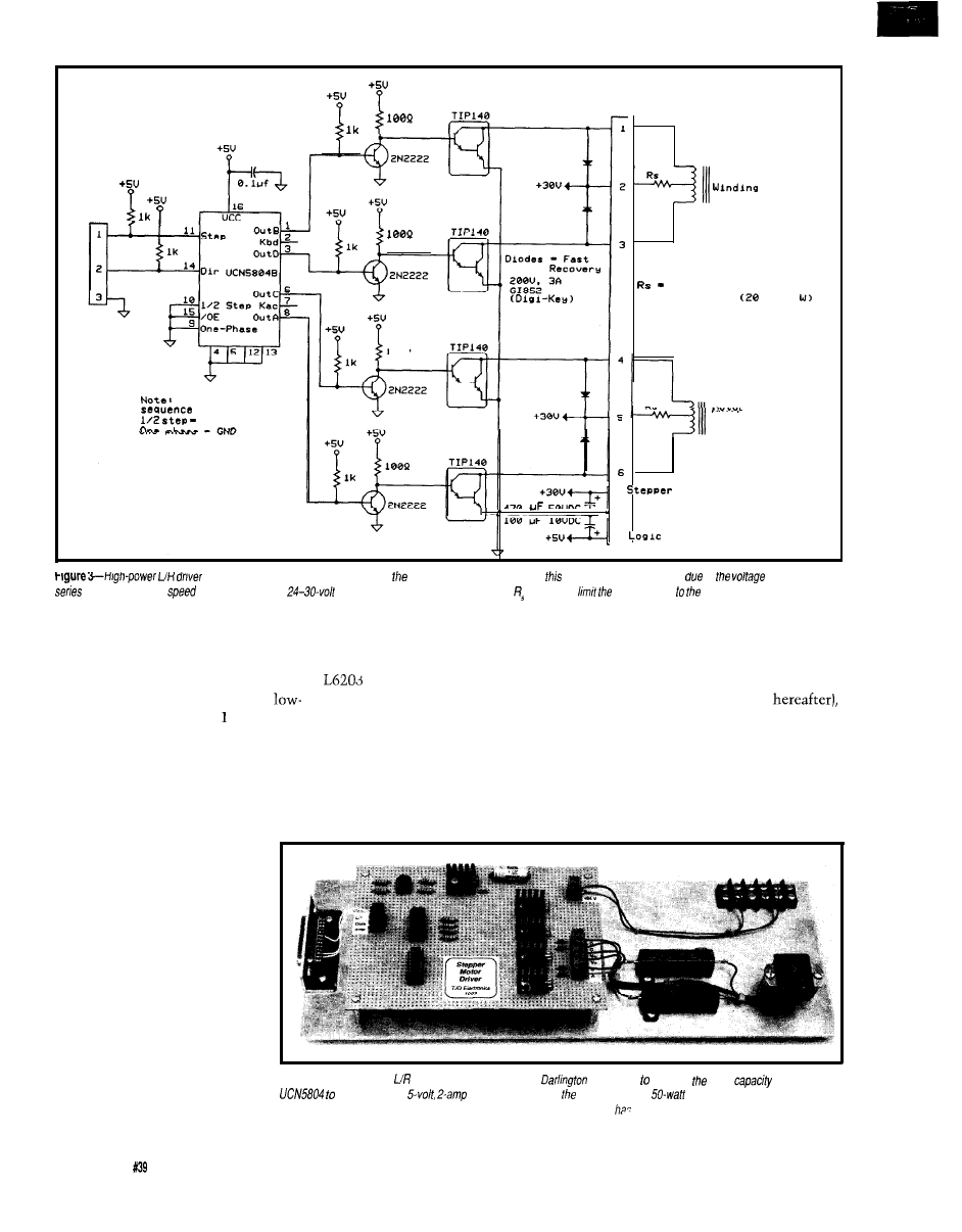
T w o - p h a s e d r i v e
p r o g r a m m e d b y
G N D
1 0 0 Q
M o t o r
1 0 t o 3 0 Q
P o w e r r e s i s t o r
t o 5 0
N o n - I n d u c t i v e
W i n d i n g
.
I
P o w e r
470
50UDC -I-
2 C o m m o n
3
P o w e r
doubles as a bagel toaster. While
offering advantage of a simple design,
circuit is wasteful or power
to
drop across the
resistors. For best
performance, use a
supply for the stepper motor and select resistors to
motor current rated value.
flowing through the collector circuit
would eventually damage or destroy
the motor. To prevent this from
happening, a circuit designed to
monitor the motor current with a
resistance [typically 0.1 to .O ohms)
sense resistor is placed in the collector
circuit. The voltage across the resistor
is used to trip a comparator. The
comparator’s threshold is set with a
I am going to discuss the L297
controller chip, which, when com-
bined with either the L298 or two
driver chips, can provide up to 4
amps of drive current per coil.
generates a set of four drive signals in
OVERVIEW OF THE SGS CHIPS
I’ll start with the L297 controller
chip (shown in block diagram form in
Figure 5). Like the UCN5804, this IC
half-step, full-step, and wave-drive
modes. An on-chip PWM chopper
circuit provides current sensing and
control. Your microprocessor needs to
provide step (called CLOCK
direction, and a few control signals
discussed later. The device is packaged
in a 20-pin DIP.
that is used to switch the motor
The outputs from the L297 are
designed to interface to a driver device
reference chosen to equal the voltage
across the sense resistor at the
desired maximum current.
Why is this approach better
than an L/R scheme? The
answer is that it eliminates the
power-wasting series resistor
and still retains a fast current
rise time by increasing the
applied voltage to the coil.
CHOPPING CHIPS
SGS-Thomson offers several
chips designed for stepper motor
applications. Of particular
interest are those that provide
Photo l--This
high-power
driver breadboard uses four
transistors increase drive
of fhe
high-power drive capability with
over 5 amps. A
motor was driven by circuit. Note the
power resistors are mounted off
a minimal component count.
the circuit board and use the aluminum base as a heat sink. This approach
the advantage of being cheap and easy to
build, but is extreme/y power wasteful.
28
Issue October 1993
The Computer Applications Journal

Users!
16 BIT
ACQUISITION?
Pulses
current. Two useful devices that can
The
(Figure 7) is the higher
power member of the chip family
be applied here are the
and
The
[see Figure 6) is a
whose members include the
dual full-bridge driver capable of
providing output current up to two
amps per coil (steady state) at up to
and
The
is a
volts. It uses bipolar transistor drivers
DMOS device capable of passing 4
in its output stage and is packaged in a
15-W
power tab package (a lower
amps at up to 48 volts. It is a single
power version, the
is available
in a 20-pin DIP). The emitter connec-
bridge device, so two are required for a
tions of the lower power transistors are
brought out to allow the insertion of a
stepper application. Because DMOS
low-value current sensing resistor for
use by the L297. Eight fast protection
diodes are required for transient
protection. I have used the
(available from
which is a
1 -amp, 200-volt type, with good
success.
Figure
chopper drive circuit uses a
source to provide an overcurrent to the motor if not con-
trotted. Control is accomplished by using a comparator
to sense voltage across a low-resistance sense resistor.
Chopping action occurs at the oscillator frequency, typi-
cal/y 20
switches are used, an intrinsic diode
exists across the source/drain connec-
tion that can act as a freewheeling
diode to protect the device from
transients. An RC snubber circuit
across the motor coil is used to limit
the voltage rise time to allow the
intrinsic diode sufficient time to act.
Figures 8 and 9 show how the
L297 controller is interfaced to the
L298 and
devices. I will take no
credit for these designs, they are
straight from the SGS data book.
have, however, built and tested them.
APPLICATION NOTES
Referring back to the L297 block
diagram in Figure 5, note the block
labeled “translator.” This block
generates the phase sequences for
step, one-phase-on (full-step], and
phase-on (full-step) operation. It is
essentially a state machine driven by a
three-bit counter that is clocked by the
A full discussion of the SGS
devices is beyond the scope of this
article and would essentially duplicate
information existing in the
manufacturer’s data sheet and applica-
tion notes. Obviously you should get
these from SGS and study them in
detail before plowing into a circuit
design. What I hope to provide here is
some amplification of subtleties.
Figure
includes aft logic required to translate step and direction
from your microprocessor to
the
sequences needed to control an external output stage. Comparators, flip-flops, and switching
needed to implement chopper control of motor current are built in.
Don’t Settle For Less
Than The Cuffing Edge.._
HIGH PERFORMANCE
Guaranteed
16 bii accuracy
6 Channel
Board
l
16 bit AID resolution
$1295
l
16 bit
throug
l
DMA
put
lines di
l
3 channe
I/O
counter/timer
LOW COST
16 bit
6 Channel
Board
l
16 bit
resolution
l
15
throughput
l
DMA
lines di
channe
I/O
counter/timer
OPTIMUM CONVERSION’”
compatible
Board
l
16 bit
resolution
l
16 bit accuracy
l
Prog. Gain
l
16
I/O
channel counter/timer
l
2
channels
395
Cut through the specs each of
16
boards have been evaluated against
every competing model. On noise
performance, speed, ease of use, and price
technology wins every time:
See for yourself Call for an evaluation
board today.
I - 8 0 0 - 6 4 8 - 6 5 8 9
We’ve been making
data
acquisition boards for longer
than anyone in the world.
70 Tower Office Park, Woburn, MA 01801
FAX
(617) 938-6553
TEL
(617) 935-6668
Analog Digital
Industrial PCs,
and High Channel Count Systems
The Computer Applications Journal
Issue
October 1993
29
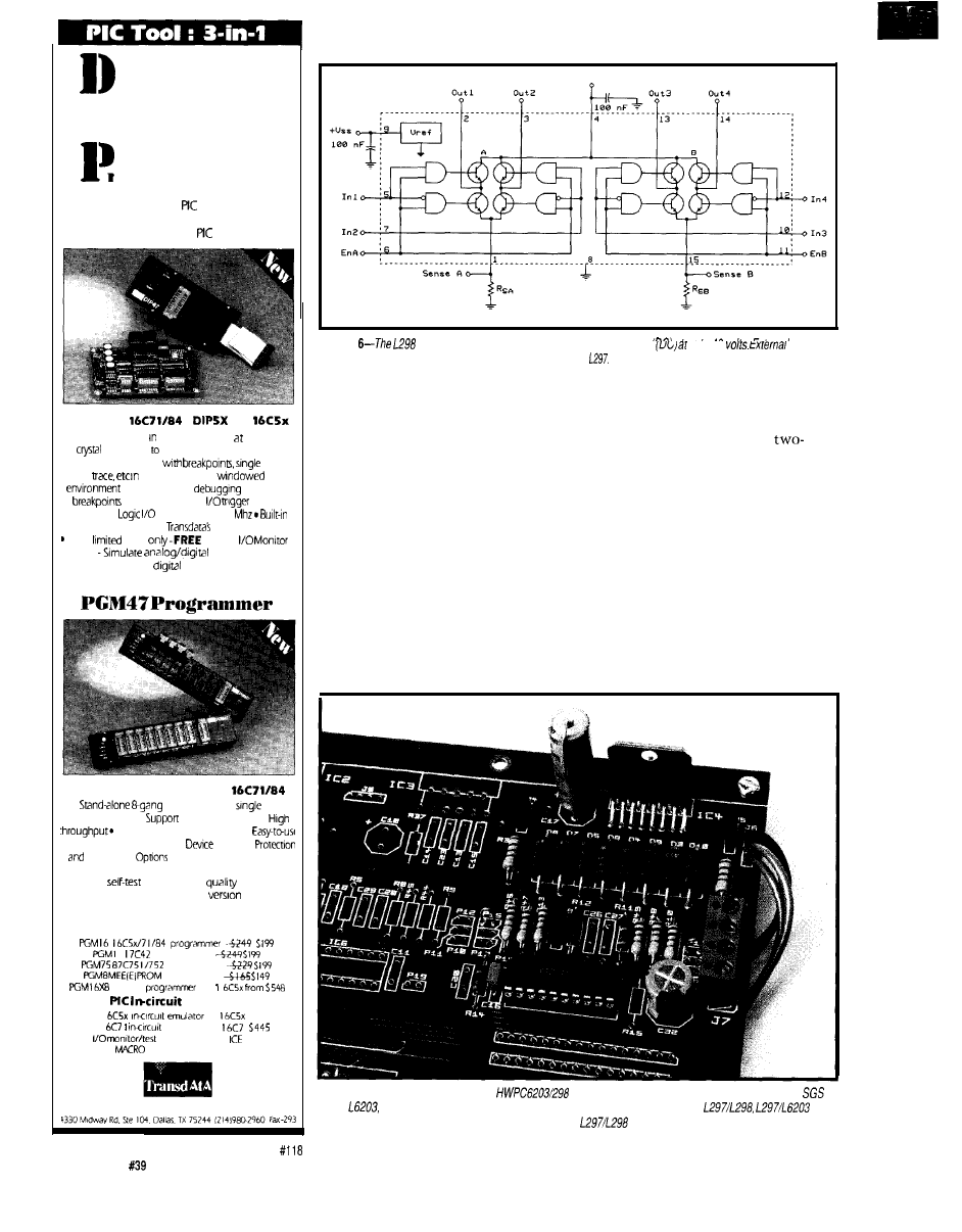
ownloader
I n-circuit Emulator
rogrammer
The Ultimate Complete
Development Tool
Packed in a
Single Hand-held Unit
for Ail
Levels of
Users
DIP47 for
.
for
l
Download
codes seconds
and run target’s
speed up 20
Mhz
l
Comprehensive
emulation controls
step,
an easy-to-use
l
Source level
.
Software
l
Hardware and
breaks
l
Real-time
capture up to
5
Programmer- Include
macro assembler
For a
time
MT I 6
Board
inputs and monitor
all
outputs
. . . . . . . .
Production Programmer for
l
or PC-hosted
unit
programmmer
l
for DIP and SOIC
l
Reliable
l
Simple operation.
copy function from Master
l
Code
Checksum
l
Program cycle Includes
blankcheck. program and byte-by-byte
verify
Power-up
l
Production
programmer
l
DIP version $499
l
SOIC
$649
. . . . , . . .
Programmers
7
programmer
programmer
programmer
-&gang
For
Emulators
ICE-l
for
5395
ICE-I
emulator for
I
MTI 6
board FREE with
purchase
ASSEMBLER INCLUDED
Advanced Transdata Corporation
Figure
is a
dual full-bridge driver capable of passing 2 amps
up ro
46
sense
resistors are used to provide current sense voltages for the
CLOCK* input. The translator output
has eight different states. When you
select the half-step mode by driving
the HALF/FULL* input high, the
translator cycles through all eight
states as the CLOCK+ input is
clocked. When you select the full-step
mode by bringing HALF/FULL* low,
the translator skips every other state
to generate either a one-phase-on or
two-phase-on drive sequence. Which
one you get is dependent on where the
state machine was when you drove
HALF/FULL * low.
RESET* low. If HALF/FULL* is low at
this time, or is brought low before a
CLOCK’ pulse clocks the state
machine, you will generate a
phase-on full-step sequence. To get a
one-phase-on full-step sequence, you
need to begin with the half-step mode
selected (
HALF
/
FULL
* = high), reset
the state machine to the first state
(pulse RESET* low), advance to the
second state by applying one clock
pulse to the CLOCK* input, and then
select full-step mode by bringing
HALF/FULL* low. All of this should
be done on initialization by your host
microprocessor.
You can force the translator’s state
machine to its first state by pulsing
Photo 2-A
photo of the SGS-Thomson
evaluation board shows an idea/ way to try out the
1297,
and L298. Three different circuits are laid out on the board including the
combinations and a DC motor driver using the L6203. The
combination has been populated in this photo.
3 2
Issue
October 1993
The Computer Applications Journal
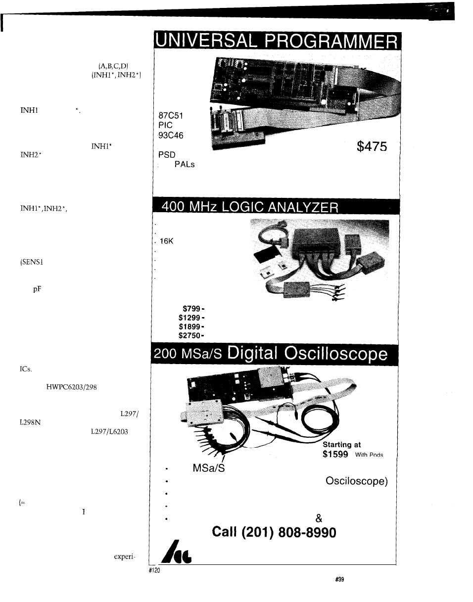
The CONTROL input to the L297
determines whether the chopper will
act on the phase outputs
or
on the inhibit outputs
to
control the drive current. Bringing
CONTROL to ground tells the L297
that you want the chopper to act on
l
and INH2 Nailing CON-
TROL high results in the phase
outputs A,B,C,D being chopped.
Normally you would want to have
the chopping occur on
and
because it would provide for a
faster current decay in the motor
windings.
The ENABLE input to the L297
must be high for normal operation of
the device. When ENABLE is low, the
A, B, C, and D outputs
are all brought low. This provides a
convenient way of disabling the motor
drive current when you want to go to a
standby mode.
The sense inputs on the L297
and SENS2) are high imped-
ance and are particularly susceptible to
glitches. I found that using a 22k and
100 low-pass filter between the
sense resistor and these inputs goes a
long way to keeping the circuits stable.
EVALUATION KITS
SGS offers several evaluation kits
for their power devices. These kits
come complete with two-sided printed
circuit boards, application notes, and
You need to add the discrete
components and solder them up.
The
evaluation
board contains three separate circuits.
Photo 2 shows the board as assembled
using the circuit in Figure 8 (the
combo]. Photo 3 shows the
implementation of the
circuit of Figure 9.
The evaluation board is designed
to run from a special PC-based driver
board. That board, in conjunction with
SGS driver software, allows you to
control the L297 from the PC. I did not
use the driver board, as I felt the cost
$300) was inappropriate to the
application. Instead, used toggle
switches to control the L297 inputs
and a function generator to provide the
step pulses.
I strongly encourage you to get
one of these kits as a means of
PAL
GAL
EPROM
EEPROM
FLASH
MICRO
XC1 736
3xx
5ns
Free software updates on BBS
Powerful menu driven software
up to 128 Channels
up to 400 MHz
Samples/Channel
Variable Threshold Levels
8 External Clocks
16 Level Triggering
Pattern Generator Option
LA12100 (100
MHz,24 Ch)
LA32200 (200 MHz,32 C h )
LA32400 (400 MHz,32 Ch)
Price is Complete
Pods and Software
LA64400 (400 MHz,64 C h )
included
& Software
200
Sampling Rate
2 Analog Channels (2ch. Digital
8 Digital Channels (8ch. Logic Analyzer)
125 MHz Single Shot Bandwidth
4K Samples/Channel (Analog Digital)
Link Computer Graphics, Inc.
369
Passaic Ave, Suite
100,
Fairfield,
NJ 07004
fax:
808-8786
The Computer Applications Journal
Issue
October 1993
3 3
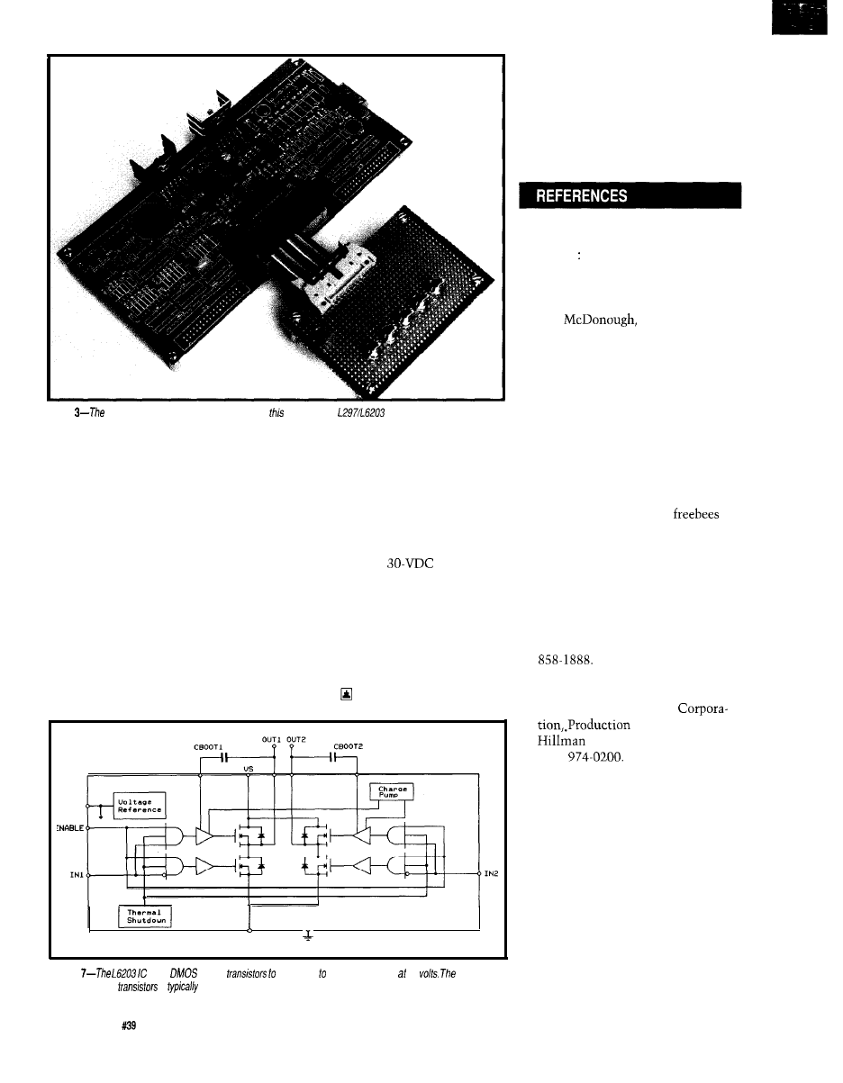
Photo
same evaluation board as in Photo 2, but
time only the
circuit has been populated.
menting with the SGS chips. Even
SOME USEFUL BUILDING BRICKS
with the evaluation kits, it is not a
Before closing, I should also
simple matter of implementation. In
mention that you can simply buy a
any circuit that is switching heavy
chopper driver module. Several
currents through an inductor, there is
companies manufacture “bricks”
going to be a tendency for glitches and
which only require a step and direction
noise. Trying to stitch wire and then
pulse on the input side, a motor on the
debug these circuits is an exercise for
the masochistic. It is much better to
start with a proven design and a clean
board layout and prove to yourself
that the circuit really works. This
allows you to quickly evaluate the
circuit, tweak what you need to, and
then do a cut and paste into your
application.
output side, and a
power
supply. They are commonly available
up to the 6-amp size in prices starting
at $150. A typical unit, rated at 2.5
amps, costs about $250. Most of the
suppliers also offer microstepping
versions as well. See the resource
section for addresses and phone
numbers.
UREF
SENSE
Figure
uses
power
switch up 4 amps of current 48
on
resistance of the
is
0.3 ohms. If is packaged in
an
eleven-lead
power tab package.
Tom Dahlin is employed as an
Electronics and Software Design
Engineering Specialist by the 3M
Company in Saint Paul, Minnesota.
His background includes 15 years of
analog and digital design, motion
control,
and electronic imaging.
Steve Ciarcia, Ed Nisley, “Circuit
Cellar Stepper Motor Scanning
Sensor A look at the logic and
control of stepper motors,” Circuit
Cellar INK, July/August 1988.
Tim
Dennis Grim,
“Stepping Out: A robot arm that
demonstrates microprocessor
control of stepper motors,” Circuit
Cellar INK, July/August 1988.
Jeff Bachiochi, “Simple Steps for
Easy Positioning,” Circuit Cellar
INK, February 1993.
TRADE MAGAZINES
Here are two useful trade maga-
zines that are offered as
to
those in the industry. Phone and
ask for a subscription request.
Motion Control-The Magazine For
Motion Control Applications and
Technology. Tower Media Corpora-
tion, 800 Roosevelt Rd., Bldg. C,
Ste. 206, Glen Ellyn, IL 60137, (708)
Motion-The Guide To Electric
Motion Control, Motion
Division, 2030
Cir., Orange, CA 92667,
(714)
SEMICONDUCTOR
DATABOOKS
The following manufacturers’
products were mentioned or used in
this article. Detailed device infor-
mation and application notes are
available in the following books:
Allegro Microsystems, Inc.
115 Northwest Cutoff, Box 15036
Worcester, MA01615
(508) 853-5000
34
Issue
October 1993
The Computer Applications Journal

22k
13
20
0 . 2 5
b e t t e r )
D o
w o u n d
Industrial
and Computer Peripheral
(2nd Ed.)
Designer’s Guide To Power Products
Application Manual (2nd Ed.)
SGS-Thomson Microelectronics
1000 East Bell Rd.
phoenix, AZ 85022
(602) 867-6100
MOTOR VENDORS
The following vendors all publish
catalogs containing specifications for
their products. Some, like
include tutorial application sections.
Stepper Motor Handbook
North American Philips
Mechatronics Group
300 West Main St.
Northboro, MA 01532
(508) 393-1919
Slo-Syn AC Synchronous, Gearmotors,
and DC Stepper Motors Catalog
Superior Electric Company
Bristol, CT 06010
combination provides up to 2
amps
per coil. Using
boost performance over that of a simple resistance
limited driver,
in
( 2 0 3 ) 5 8 2 - 9 5 6 1
Dower efficiency.
Prize Winning PC
Software!
Virtual Reality
for IBM/PC
VIRTUAL REALITY TUTOR
Easiest
way to quickly learn about this fascinating new
technique... includes a working Virtual
Reality
Game your class can play. $59
PC
THERAPIST IV Animated
talking head talks through the PC speaker!
First software to pass a limited Turing Test of
conversational ability at the Boston Computer
Museum.
$69
Sound
Blaster
version available
$18.95
BOTH
Includes 3 BIG catalogs and FREE Talking
Expert System Demo! Please specify disk size or we ship 3.5”.
Check, American Express or P.O. to:
For
more information Phone (718)
P.S. Do you teach? Make computing come alive for you
students! Order our
4 disks,
manual, Information on request.
Cross Assemblers
Extensive arithmetic and logical operations
Powerful macro substitution capability
Unlimited include file capability
Selectable
hex or
Motorola hex object
format
Simulators
Ten user-definable screens
Unlimited breakpoints and memory mapping
Trace
file to record simulator session
Disassemblers
substitution of defined
names for all
and
branches
Automatic insertion of supplied comments and expressions
716 Thimble Shoals Blvd.
Newport News,
VA 23606
(804) 873-1947
873-2154
BBS (804)
I
October

“DC
L 6 2 0 3 2
Figure
combination
provides up to 4 amps per coil. Special care needs to be taken on power trace
wiring and board layout The values of the sense resistors are chosen such that the
drop across them be
about
at
the operating current of the motor.
We solve your stepper
motor problems!
Recently, a major manufacturer came to us with a problem:
Design a multi-tasking program that would handle any
number of centrally-controlled stepper motors and product
sensors, and make it all work at very high speed.
RESULT:
A highly workable system that operates
efficiently and reliably so that products come out right
the first time. Our software designers know how to
solve your problems quickly!
Hundred Acre Consulting
5301 Longley Lane Suite D-144
Reno NV 8951 l-1 805
+I-702-829-9700
Oriental Motor USA
(Vextra Brand Motors)
2701 Plaza Del Amo, Ste. 702
Torrance, CA 90503
(213)
American Precision Industries
Division
3229
Rd.
Oceanside, CA 92054
(619) 439-7500
SURPLUS HOUSE
C&H Sales
2176 East Colorado Blvd.
Pasadena, CA, 91107
(800) 3259465
BOOKS
Theory and Application of Step
Motors, Kuo, B.C., West Publishing,
1974.
Stepping Motors: A Guide To Modern
Theory and Practice,
2nd Edition, P.P.
Acarnley, Peter Peregrinus LTD,
London, UK, 1984.
Motors and Controls,
James T.
Humphries, Merrill Publishing
Company, Columbus Ohio, 1988.
READY-TO-GO STEPPER
DRIVERS
The following companies offer
to-go stepper motor drivers in the form
of packaged modules.
Intelligent Motion Systems, Inc. (IMS)
5 11 Norwich Ave.
Taftville, CT 06380
(203) 889-8353
Semix, Inc.
4160 Technology Dr.
Fremont, CA 94538
659-8800
General Controls, Inc.
2350 Brickvale Dr.
Elk Grove Village, IL 60007
(708) 595-2152
404 Very Useful
405 Moderately Useful
406 Not Useful
36
Issue
October 1993
The Computer Applications Journal

Derek Matsunaga
Data Logging Meters are
No Fluke
espite the
relative age of the
80 series of Fluke
multimeters, they
remain one of the most versatile and
popular hand-held
available
today. Their rugged design, ease of use,
and wide range of features makes them
a first choice among many engineers.
Unfortunately, these meters are not
known for their data acquisition
capabilities.
After removing my Fluke 87 from
its familiar yellow holster, I noticed
the “quick reference card” molded into
the back of the meter. One of the
features listed on this card is labeled
“Ultrasonic Data Output,” which is
enabled by pressing the HOLD button
while turning the meter on. With this
feature enabled, I noticed that the
meter emitted an audible buzz each
time the display was updated. As it
turns out, the Fluke 80 series
multimeters have the capability to
audibly transmit information via their
internal speakers. A project was born!
I immediately assumed that the
buzzing noise was numerical data
representing what the meter was
measuring. After building an audio
detection circuit, I began to analyze
the transmitted information to
determine the data format. I started by
looking for some sort of BCD or
similar format-to no avail. After
many hours of staring at the data, I
finally figured out that each bit of data
represents an active segment on the
meter’s display.
Once I determined the data
format, I added a
to the
detection circuit and wrote software to
translate the information from the
meter’s format into ASCII. With the
completed circuit and software, all
information on the meter’s display is
transmitted via RS-232 to a host. This
data can be viewed remotely on a
dumb terminal, printed on a printer, or
logged to disk for later processing. In
this way, the Fluke 80 series becomes
a front end to a computer-based
measurement system. Not bad for free!
I should note that Fluke does not
support this function as an end-user
application. They do not disseminate
any information about this output
capability or its data format. They’ve
told me that the ultrasonic output
capability is used strictly for final
testing of the unit at the factory and is
not intended for data acquisition.
However, it’s already built into your
80 series, so why not use it?
I’ll begin by explaining the basics
of the meter’s data format. The details
of the data format are, unfortunately,
pretty complicated and cannot be fully
described in such a short article.
Following the data format, I’ll discuss
the signal detection scheme and the
microprocessor hardware. The hard-
ware discussion will be followed by an
outline of the software. I’ll conclude
by describing some of the applications
for this project.
THE 80 SERIES DATA FORMAT
With the ultrasonic output
enabled, the meter transmits the
displayed data via its internal speaker.
Naturally, all other audio indicators
are nonfunctional when the meter is in
this mode. The data output is heard as
a buzzing noise which occurs about
twice every second, depending on the
measurement mode of the meter.
When in Ultrasonic Output mode, the
measurement rate of the meter is
reduced by about half. Each occurrence
38
Issue
October 1993
The Computer Applications Journal
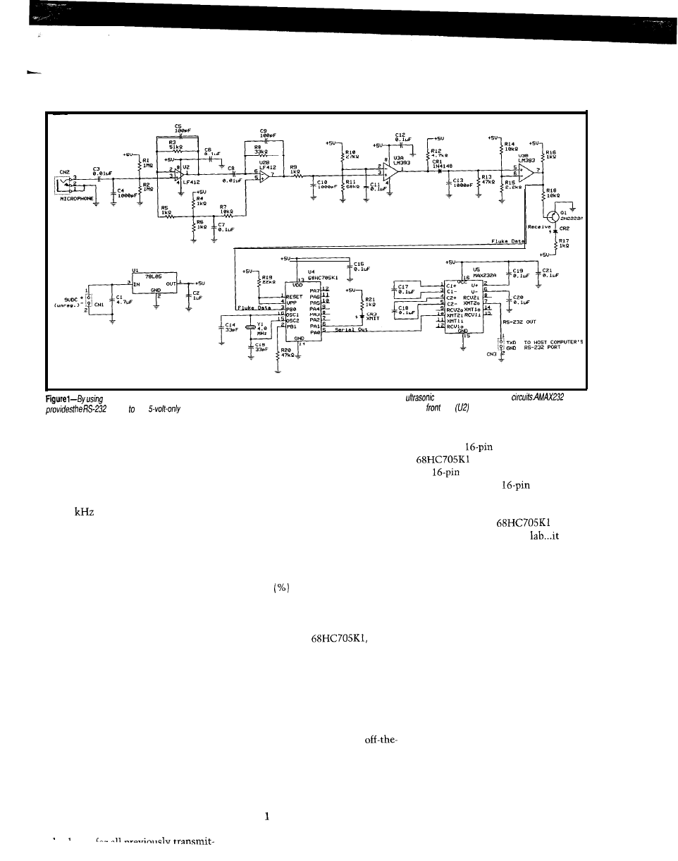
a single-chip microcontroller for the brains, the bulk of fhe Data Holster circuitry consists of the
front end and
smoothing
interface allow
operation. If the interface is plugged directly into the meter, the microphone
end
may be eliminated.
of the buzzing sound represents a
string of thirty-six nybbles that
contain information about which
segments and annunciators are active
on the meter’s display.
The output signal is modulated on
a 16.6
carrier. The bit time is
about 1.3 ms. Each nybble is lead by a
start bit (logical 1) and terminated by a
stop bit (logical 0). This allows fairly
accurate asynchronous detection
because a word counter can be reset
every time a start bit is received, thus
eliminating timing error stack-up.
With the start bit, the stop bit, and
four data bits each taking about 1.3
ms, the total time to transmit a single
word is 7.8 ms. Since there are 36
words per data string, each string will
require a total of about 280 ms of
transmission time. The time between
data strings varies with the meter’s
measurement mode, but it is always at
least one word length. I used 11 ms
(about 1.5 word lengths) to detect dead
time between measurements.
Each string of data contains a
three-word header and a one-word
trailer, which leaves 32 words for
actual measurement information. I’m
not sure what the function of the
header is, but the trailer word is a
ted words in the string. Perhaps the
header could be used for synchroniza-
tion in case the bit time were to
drastically change.
Each bit of the 32 data words (128
bits total) indicates the status of a
specific segment or annunciator on the
meter’s display. The bar-graph seg-
ments are included in the transmis-
sion. Unfortunately, the meters in the
80 series do not share a common data
format, For example, the percent
indicator
on the Fluke 85 trans-
lates into the Hertz (Hz) symbol on the
Fluke 87. Clearly, the two are not
interchangeable. Because of the ROM
limitations of the
I wrote
separate software for each meter in the
80 series to address the differences in
data format.
HARDWARE DESCRIPTION
In designing the hardware for this
project, my major constraint was to
build a circuit using common
shelf components while minimizing
the circuit’s physical size. My ultimate
goal was to build a self-contained unit
which could easily attach to the meter
with no electrical connection (see
Photos and 2). Additionally, I wanted
to use a DC wall transformer as a
power source. The size constraints and
power source requirements lead me to
choose the
Motorola
for a microcontroller, and
the
MAX232 for driving RS-232.
In addition to their
footprints,
these two devices require just a few
external components to function.
Luckily, I had the
evalua-
tion kit sitting idly in the
was a
processor looking for a project!
SIGNAL DETECTION
The key to signal detection in this
project is the use of a suction cup
microphone to pick up the meter’s
signal. This microphone, typically
available at Radio Shack, is designed to
be attached to a telephone handpiece
for conversation recording. Its unidi-
rectional characteristics inherently
filter background acoustical noise and
require the signal source to be in close
proximity. However, this microphone
can be excited by electrical noise from
all directions. I’ll discuss the effects of
electrical noise on the detection
circuit after describing the system
hardware. For now, assume the
microphone will only pick up acoustic
signals.
The schematic for this project is
shown in Figure 1. With the micro-
phone attached to the back of the

ing software description,
explain
how I dealt with some of the Kl’s
limitations and how all of this func-
tionality was crammed into 496 bytes.
Due to the Kl’s small ROM space,
it was necessary to select which of the
meter’s annunciators would be
decoded and which would not. Since
each
and each annunciator
requires at least
software compari-
son and one ASCII character, some of
the least-used annunciators had to bc
eliminated. Of all possible numerals
and annunciators that the meter is
capable of displaying, I
selected to decode and
transmit the following:
and the necessary variables are
initialized. The program then loops
until about
11
of dead
at port
B bit 0 is detected. In other words, the
program will not start acquiring a data
record from the meter unless it can
acquire the entire record rather than
just a record fragment. Since the
executes an instruction every 500 ns
(remember the
internal clock),
a
register is
to count
ms of
time. The
lacks such a
so I did
counting by incre-
menting the lower eight bits and, upon
*numerals 0 through 9
and decimal points
*polarity signs and
available magnitude
prefixes (u for micro,
n for nano, M for
etc.)
available unit
suffixes (V for volts, F
for Farads, Hz for
Hertz,etc.)
*the AC and DC
annunciators
overflow, incrementing the upper eight
bits. Although this task is fairly trivial,
it consumes precious ROM space!
When about 11 ms of dead time
has been detected, the program
proceeds to acquire the 36 four-bit
words from the meter. Each time a
start bit is detected, a counter is reset
and
software looks at port B for a
duration. The number of highs
and lows detected during this time are
stored in separate locations. This
enables the software to “filter” noise
which may be caused by the meter’s
deviation from the
ms bit time. At the end
of the
bit time,
the software checks to
see if
were more
highs than lows. If so,
the bit is considered to
asserted.
If the most
Wait
between
Acquire and store
a nybble
arc probably
for most
applications. Among the
annunciators which I
had to eliminate are the
bargraph,
the low-battery indica-
tor, the
indicator,
and the
AVG-RECORD indica-
tors. Most of the
eliminated annunciators
do not have significance
pertaining to the actual
measurement on the
Load ASCII value
for
Check for
overload (OL)
meter. After making
these sacrifices, the code
was ready to be written.
Figures 3a and 3b for
the software flowchart.
Load ASCII value
The
program
counter is vectored to
address
hex upon
an external
or
power up. At this point,
the ports are configured
meter’s checksum. If
they do not match, the
software loads the
ASCII value for an
exclamation point (21
hex) and sends it out to
Figure
code
takes up 496
bytes of
ROM
and
32 bytes of
RAM contained
in fhe
Due the limited nature of
microcontroller, most things are done brute
force
with straight-line code.
recently received bit is
a start bit or a stop bit,
it is ignored and the
software waits until
the next bit is received.
the bit is
rolled onto an
byte and stored in
RAM for later process-
ing. This process is
repeated until all 36
words have been
received. Although the
process of converting
bit words into the
structure of the
is
fairly straightforward,
the required house-
keeping activities eat
up many bytes of
ROM...and we haven’t
even started to decode
the data yet!
After receiving the
36 words sent by the
meter, the software
runs an algorithm on
the data and compares
the result with the
The Computer Applications Journal
Issue
October 1993
4 3

meter, the
modulated
signal is routed through CN2
to conditioning amplifier
This amplifier detects
changes in the pickup’s
impedance, eliminates any
DC which may be present,
and amplifies the signal. The
amplified signal is then sent
through another gain stage in
The resistor divider
formed by R4 and R6 pro-
vides a DC reference at
to
the inputs of U2, allowing
AC-coupled operation of the
op-amps with a single +5-V
power supply. Small capaci-
tors in the feedback paths
reduce the frequency re-
sponse of the op-amps to
prevent high-frequency
Conditioned signal from meter (U3, pin 1)
1 b i t
ov
Peak detector output
pin 5)
U3, pm 6
ov
signal (U3, pin 7)
ov
figure
signal from meter is first squared up, then passed through a
peak detector. The final output is then used bv the microcontroller to decode the
oscillation. After the
d a t a t r a n s m i s s i o n .
microphone’s signal has been
amplified, it is lightly filtered by R9
and
At this point, the signal is approxi-
mately 1.5 volts (peak to peak) riding
on the
offset. Comparator
is
used to square-up the
16
signal so
that it swings between ground and
Vcc. The “squared-up” signal then
feeds the peak detector formed by
R13, and C13. The cutoff
frequency of this peak detector is set
to about 21
by Cl3 and R13 while
the peak voltage is limited by the
divider formed by
and R13. This
ensures that the peak detector will
never charge to V, but will dis-
charge fast enough to prevent stretch-
ing out the bit time. Figure 2 shows
the critical signals in a typical bit
detection sequence.
The output of the peak detector is
“squared-up” by
to
levels. The detected signal is then fed
into port B, bit 0, of the
Transistor
lights CR2 every time a
bit is detected. I added this to the
design for troubleshooting and visual
effect purposes.
MICROCONTROLLER HARDWARE
The
herein after
referred to as
is an extremely
simple
microcontroller. With its
built-in RAM, ROM, and ports, it
requires very few external components
to
function. Namely a crystal, some
capacitors, and a few resistors.
The crystal frequency of the is
4 MHz. The divides this frequency
by two internally for a resulting
operating frequency of 2 MHz (500 ns
per cycle). Interrupts (either software
or hardware) are not used in this
project.
The reads the detected signal
at port B bit 0, decodes it, and trans-
lates the decoded data into ASCII. The
ASCII data is then placed on port A bit
0 via a software shift register at 9600
bps, 8 data bits, one stop bit, no parity.
The serial data is then passed to
[the MAX232) for level shifting. The
LED on port A bit 1 flashes every time
a data string is sent out.
ADDITIONAL HARDWARE NOTES
As I mentioned earlier, the
suction-cup microphone can be excited
by electrical sources. Although I do
not have complete data on the micro-
phone (it came from Radio Shack), I
assumed that its internal construction
is similar to that of a loop antenna.
This presents a problem when the
microphone is in close proximity to
video monitors, computers, or other
strong sources of
To eliminate
this, I have experimented with adding
filters (both active and passive) to the
front end of the detection circuitry.
This turns out to be a fairly
difficult task because of the
sharp
required to
attenuate all noise sources
while only passing the
carrier. A
filter
centered around 16
with
attenuation of maybe 40 or
50 at 15 and 17
would probably eliminate
most of the electrical
interference. However, I
don’t believe these specifica-
tions can be reasonably met
without using DSP tech-
niques. Whether analog or
digital, an effective filter
would add a significant
amount of complexity to the
system.
A simpler way to
eliminate noise problems is
to
the meter’s
speaker output to the decoding circuit.
To use a
connection, you
must install a connector in parallel
with the meter’s speaker. Casual users
will probably not want to modify their
meters in this way, but it is a must for
serious users. I used a
phone jack
mounted just above the V+ jack on the
meter (refer to Photo
I wired my
meter such that when a
phone plug
is inserted into the jack, the internal
speaker of the meter is disabled. This
makes for silent and reliable operation
(the continuous audio information
emitted by the meter can become
quite annoying after a while).
If a
connection is used,
the microphone front end of the
decoding circuit (U2) can be elimi-
nated. However, it is important to
electrically isolate the meter from the
decoding circuit to protect the circuit
in case the meter fails to provide
isolation between its input jacks and
the speaker. I used a pulse transformer
in a DIP package for this purpose. The
output of the pulse transformer can be
connected directly between ground
and U3 pin 3. In doing this, be sure to
protect the input of U3 with diodes
because the transformer’s output will
swing below ground. Also, the thresh-
old voltage at U3 pin 2 may have to be
adjusted depending on the turns ratio
of your transformer.
4 0
Issue
October 1993
The Computer Applications Journal

comfortably
behind
the
shockcase
with no
to
From to
along the side of the
are the receive indicator,
indicator,
power indicator,
and
output
jack
The easiest way to eliminate noise
problems is to move the meter and
decoding circuit away from the
suspected noise source. If the micro-
phone is swamped with noise, the
(CR1 and CR2) will not flash
because the peak detector is probably
pegged high. The decoding software in
the uses the meter’s checksum to
detect intermittent noise. If a bit gets
corrupted during transmission, the
software will transmit an exclamation
point to the host computer to indicate
that an error has occurred.
On my initial prototype,
I
used
supplies generated by the
MAX232 to power the LF412. At the
time, it seemed like an elegant
way to provide a dual rail supply to
op-amp. This scheme worked quite
well until I replaced the Maxim part
with one of its alternate sources. A
S
luck would have it, the source imped-
ance of the non-Maxim
supply
ultrasonic connection is too unreliable or
connection of the
The
jack can be Seen
above
The New Shape
of
Embedded PCs
The amazing
is
complete
200% PC-compatible
single
board computer
measuring only 3.6” by
14
MHz
n
CGA/LCD controller
l
2M DRAM
ROM-DOS kernel
n
bootable 1 M solid-state disk
configuration EEPROM
1
IDE controller floppy interface
n
PCMCIA interface
n
two RS-232, one RS-485 parallel
n
XT keyboard & speaker
watchdog timer
n
volts only operation
Designed
for
low power applications,
the
draws one watt
which drops to 350 milliwatts in sleep
mode, 125 milliwatts in suspend mode.
Free utility
software
lets your
application boot
from
ROM!
RTD also offers a complete line of
peripherals for expansion:
1.6” hard drive PCMCIA carriers
n
data acquisition modules
n
opto-22 digital
modules
VGA CRT/LCD interface
For more information:
call, write
or fax
us today!
Place your order now and receive a
CM102 PCMCIA carrier module
FREE!
Real Time Devices, Inc.
P.O. Box 906
State College, PA 16804
(814)
n
Fax:
(814) 234-5218

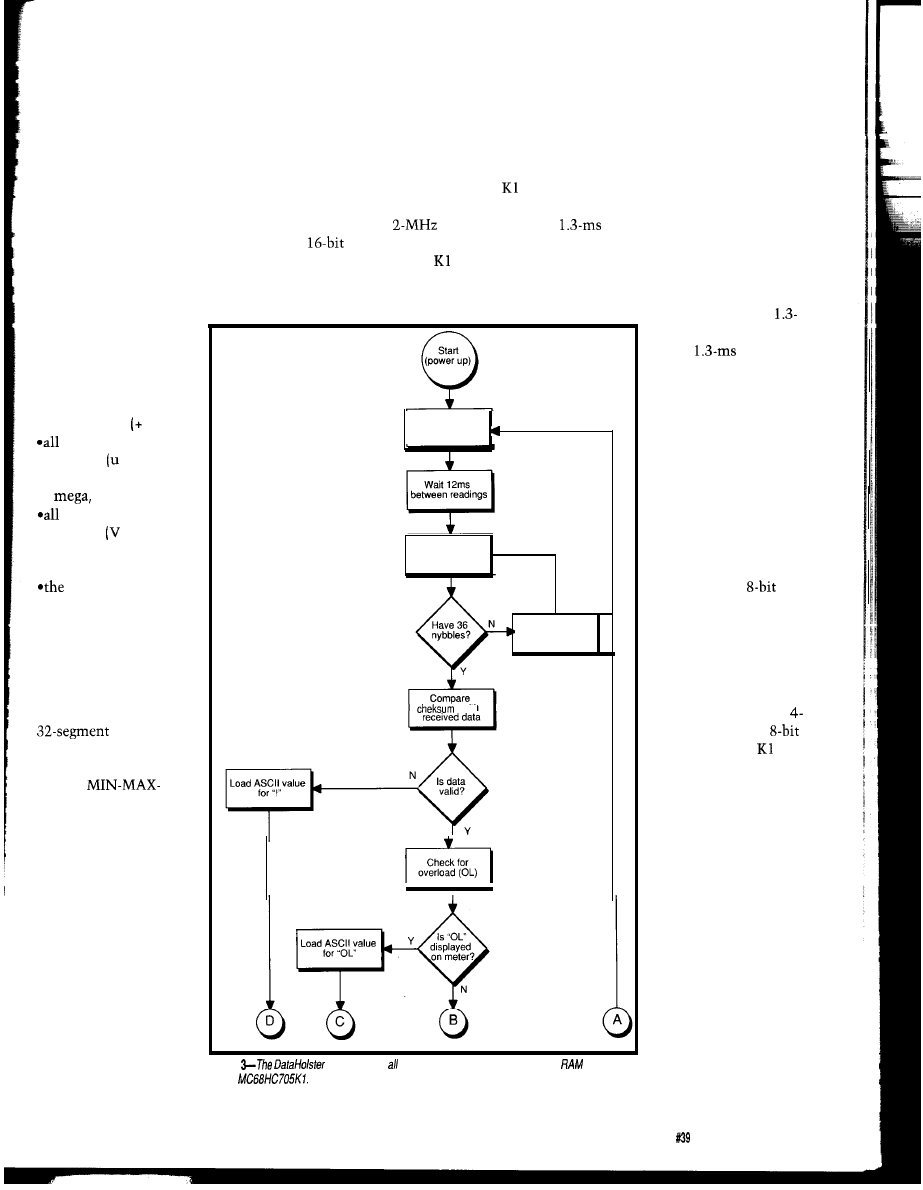
capable of displaying, I
selected to decode and
transmit the following:
*numerals 0 through 9
and decimal points
*polarity signs and -)
available magnitude
prefixes for micro,
n for nano, M for
etc.)
available unit
suffixes for volts, F
for Farads, Hz for
Hertz,etc.)
AC and DC
annunciators
These are probably
sufficient for most
applications. Among the
annunciators which I
had to eliminate are the
bargraph,
the low-battery indica-
tor, the beeper indicator,
and the
AVG-RECORD indica-
tors. Most of the
eliminated annunciators
do not have significance
pertaining to the actual
measurement on the
meter. After making
these sacrifices, the code
was ready to be written.
See Figures 3a and 3b for
the software flowchart.
The Kl’s program
counter is vectored to
address 0200 hex upon
ing software description, I’ll explain
how I dealt with some of the Kl’s
limitations and how all of this func-
tionality was crammed into 496 bytes.
Due to the Kl’s small ROM space,
it was necessary to select which of the
meter’s annunciators would be
decoded and which would not. Since
each numeral and each annunciator
requires at least one software compari-
son and one ASCII character, some of
the least-used annunciators had to be
eliminated. Of all possible numerals
and annunciators that the meter is
an external reset or
power up. At this point,
the ports are configured
and the necessary variables are
initialized. The program then loops
until about 11 ms of dead time at port
B bit 0 is detected. In other words, the
program will not start acquiring a data
record from the meter unless it can
acquire the entire record rather than
just a record fragment. Since the
executes an instruction every 500 ns
(remember the
internal clock),
a
register is required to count 11
ms of dead time. The lacks such a
register, so I did the counting by incre-
menting the lower eight bits and, upon
overflow, incrementing the upper eight
bits. Although this task is fairly trivial,
it consumes precious ROM space!
When about 11 ms of dead time
has been detected, the program
proceeds to acquire the 36 four-bit
words from the meter. Each time a
start bit is detected, a counter is reset
and the software looks at port B for a
duration. The number of highs
and lows detected during this time are
stored in separate locations. This
enables the software to “filter” noise
which may be caused by the meter’s
Initialize
Registers
Acquire and stare
a nybble
l
Increment nybble
counter
with
Check for
overload (OL)
Figure
code takes up 496 bytes of ROM and
32 bytes
of
contained
in the
Due to the limited nature of the microcontroller, most things are done brute
force with straight-line code.
The Computer Applications Journal
deviation from the
ms bit time. At the end
of the
bit time,
the software checks to
see if there were more
highs than lows. If
SO
,
the bit is considered to
be asserted.
If the most
recently received bit is
a start bit or a stop bit,
it is ignored and the
software waits until
the next bit is received.
Otherwise, the bit is
rolled onto an
byte and stored in
RAM for later process-
ing. This process is
repeated until all 36
words have been
received. Although the
process of converting
bit words into the
structure of the is
fairly straightforward,
the required house-
keeping activities eat
up many bytes of
ROM...and we haven’t
even started to decode
the data yet!
After receiving the
36 words sent by the
meter, the software
runs an algorithm on
the data and compares
the result with the
meter’s checksum. If
they do not match, the
software loads the
ASCII value for an
exclamation point (2 1
hex) and sends it out to
Issue October 1993
43
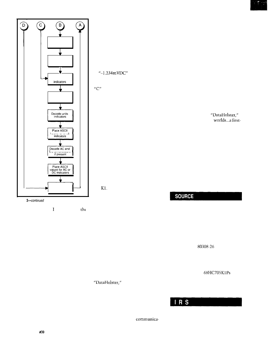
B
Decode numerals
and decimal pts.
,
Place ASCII
values for
numerals
Decode
magnitude
,
Place ASCII
values for mag.
indicators
values for units
DC annunciators
Place ASCII
values for AC or
DC indicators
Send serial output
buffer to Port A
Figure
the host computer. could not use
word “error” because it requires 5
bytes of ASCII and some overhead to
transmit, so I used the exclamation
point instead.
If the checksum algorithm
determines that the data is valid, the
software proceeds to decode the
meter’s display. It begins the decoding
by checking for an overload condition
on the meter. This condition is
indicated by the letters “OL” on the
meter’s display. If the software detects
the seven-segment signature of “OL,”
it will not try to decode the polarity
sign or any numerals.
The software decodes the data in
the same order that you would read
the meter...from left to right. The
polarity sign is decoded, followed by
the ten-thousands digit, followed by
the thousands digit, followed by the
hundreds digit, and so forth. After
decoding the polarity and the numer-
als, the software looks for magnitude
indicators and units indicators.
Finally, the “AC” and “DC” annun-
ciators are decoded. This decoding
method allows the appropriate ASCII
values to be placed in the serial output
buffer in the order in which they are
to be transmitted. So, a reading such
as
will have the
ASCII value for a minus sign at the
top of the serial buffer and the letter
at the bottom. This makes the
serial output routine fairly simple.
After decoding all of the data and
storing the appropriate ASCII values
in the serial output section of RAM,
the software enters the serial output
routine. This routine simply loads a
character from the serial output
section of RAM and shifts it, bit by
bit, into port A. When the bit shifting
is complete, a stop bit is sent and the
process repeats until all characters in
the serial output section of RAM have
been sent. The serial output routine
sends a carriage return after the last
character is sent. When the RS-232
transmission is complete, the program
loops back to the beginning and starts
over as if power were just applied to
the
Embedded within the software are
a couple of neat tricks which I used to
reduce the program size while main-
taining full functionality. Unfortu-
nately, they are too detailed to explain
here. A complete listing of the Fluke
83 version of the software, including
comments, is available on the Circuit
Cellar BBS.
APPLICATIONS
The applications for this project
are numerous because the Fluke 80
series is an extremely versatile (and
popular) hand-held multimeter capable
of making true RMS measurements.
This project, affectionately named the
can be used as an
automated data logger for environmen-
tal measurements such as temperature
(with a thermal probe], humidity,
motor RPM modulation, long-term
power line monitoring, or any other
slow-moving signal. By using a
computer with RS-232
tions software, the data from the meter
can be captured as a function of time.
This data can be stored for off-line
postprocessing in a spreadsheet,
graphing program, or database.
CONCLUSIONS
This project illustrates how to use
the little-known ultrasonic output
feature of the Fluke 80 series for data
acquisition. Since the introduction of
the 80 series, many hand-held meters
have been introduced which sport
some kind of computer output capabil-
ity. However, the measurement
capabilities, accuracy, and reliability of
these other meters may not be on par
with that of the 80 series. Using the
Fluke 80 series with a
you get the best of both
class, time proven, true RMS, hand-
held multimeter, and data acquisition
capabilities!
q
Derek Matsunaga holds a BSEE and is
currently a product engineer for a
medical device design/manufacturing
company. His interests include circuit
design and analysis, product develop-
ment, and signal processing. He may
be contacted at the address below
OK
on the Circuit Cellar BBS.
A complete technical description
of the Fluke 80 series data format
with drawings and examples may
be ordered by sending a check or
money order for $9.95 (U.S.) to:
Derek Matsunaga
P.O. Box 19615
Boulder, CO
15
A hardcopy of the commented
sourcecode will also be included.
A limited quantity of program-
med and tested
for
this project is available. If
interested, please inquire when
ordering technical information.
407 Very Useful
408 Moderately Useful
409 Not Useful
4 4
issue
October 1993
The Computer Applications Journal

DEPARTMEN
Firmware
From the Bench
Silicon Update
Embedded
iiques
Patent Talk
TS
The ‘386SX
Gets Positive
Identification
and a Small
Display
and
Ed Nisley
ome years ago
serial numbers so
software could be keyed to a single PC.
The predictions were that software
piracy would die overnight, profits
shoot up, prices drop down, and all
would be right with the world.
Another prognostication gone
awry.
At the moment I suppose I’m one
of those software pirates, because
I
have two PCs: a dying Model 80 from
which I’m transferring files to my new
system. If the PCs had unique serial
numbers I’d be out of luck even
though I’ve got only one pair of hands
on one keyboard at any one time...and
the Model 80 can no longer run the
programs.
Actually, it gets worse. The first
new system didn’t quite work, so this
is actually my second attempt to
transfer the files. It’s never been clear
what the software transfer fee might
be in this situation, but I’m sure
paying it twice wouldn’t improve my
disposition at all.
Nevertheless, this month I’ll
describe how to give your Firmware
Development Board a unique ID based
on the Dallas DS2400 Silicon Serial
Number. If you combine the (almost
trivial) hardware with the BIOS
extensions from last month’s column,
you can produce a system that won’t
even boot with an incorrect serial
number, let alone run a program. Just
don’t try to charge me for your code,
OK?
We’ll also add a small,
LCD panel to display status messages
without a terminal or video monitor. If
46
Issue October
1993
The Computer Applications Journal

Figure l--The
uses a single
output bit
and one input bit, but the LCD pane/ needs a
byte of data
and several control lines. of the pulse timings are produced in firmware, so these devices are not connected
to
the
ISA bus connector. Previous columns have presented the
circuitry behind these
naught else, it can point out a wrong
is bit-serial, while the LCD uses a
serial
perhaps show an
byte-wide parallel port. We’ll use the
unchanging “33” so everyone knows
Firmware Development Board’s 8254
your PC’s clock rate.
timer chip to provide
The two devices require
dent timings, plus a dollop of test code
pletely different interfaces: the DS2400
to make sure everything is working.
The DS2400 claims to use a
one-wire interface. You need a
ground connection, of course,
but one signal wire provides
bidirectional data and timing.
Both the 7407 open-collector
driver and the DS2400 can pull the
wire to ground, while the
resistor supplies the logic-high state
when the driver transistors are off.
As you might expect from a
CMOS part, the DS2400 does not use
TTL voltage levels. Its
rating is 3.0
volts, which is well above the 2.4 volt
of normal TTL. The part is always
used with an open-collector driver and
so this has no effect on most
circuits, but keep it in mind if you’re
trying something truly bizarre.
The LCD interface has more wires
and a contrast-control
but it’s
fairly simple. In fact, you can probably
connect the
terminal to ground for
acceptable contrast without a pot. If
your LCD panel requires a negative
bias voltage, connect the pot between
the and -12 power supplies. You
should increase the pot to about
to
reduce its power dissipation or, better
yet, follow your LCD’s data sheet
recommendations.
Photo l--The
looks
like a plastic transistor just below the 8254, while the LCD port connects to the ribbon
cab/e going off the top of the board.
SIMPLE CIRCUITRY
The DS2400 and character
LCD interfaces require very
little additional hardware, as you
can see in Figure As before,
I’ve omitted the ISA bus connec-
tions and support chips de-
scribed in previous columns, so
you’ll need to refer back a few
issues to get the complete
details.
Photo 1 shows the Firmware
Development Board as it looks
today. The DS2400 looks like a
plastic transistor in a TO-92 case
just below the 8254, while the
LCD port connects to the ribbon
cable snaking from the top of the
picture. The lithium cell,
MAX691, and the clump of
discrete parts provide backup
power for the SRAM chip
located in the upper right comer
of the board.
A perennial BBS question involves
interfacing these little LCD panels
directly to a microcontroller bus. The
The Computer Applications Journal
Issue
October 1993
4 7
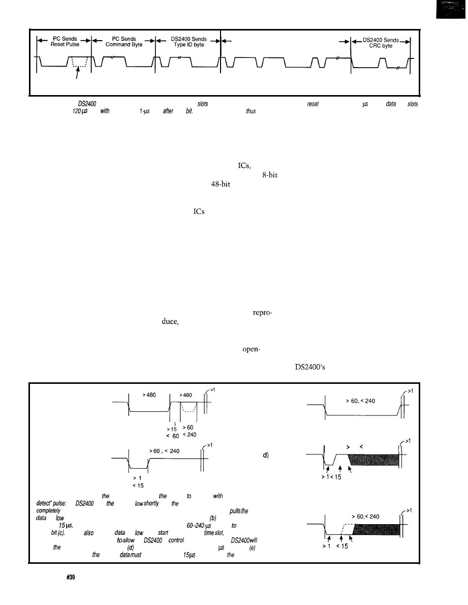
DS2400 Sends 6 byte Serial Number
DS2400 Sends 6 Byte Serial Number
Figure P-Reading a
requires a reset pulse
followed by
72 time
for the bidirectional data flow. Each half of the
pulse is at least 480 and the
time
are between 60 and each
a mandatory
delay
each A complete transaction
occupies less than 10 ms.
Hitachi HD44780 LCD controller is
really designed for the 6800 family
bus, so it takes a bit of hocus-pocus to
adapt it to an Intel bus. Rather than
confront that issue, I elected to use
simple port I/O and be done with it. If
you need just an LCD panel without
all the rest of the Firmware Develop-
ment Board, the references I men-
tioned in Issue 3 1 should give you a
good head start on your bus interface
design.
Be careful when you wire up the
LCD’s ‘245 and ‘374 data lines. It’s
quite easy to get one group “back-
wards” and produce some truly
baffling bugs. The LCD software
includes a counting sequence that
should help pin down that problem,
but it’s better to avoid it entirely. Note
that the ‘374 driving the LCD’s data
BIDIRECTIONAL BIT BANGING
Each Dallas Semiconductor
DS2400 Silicon Serial Number chip is
laser-personalized during production
so that, unlike ordinary
every one
is unique. The data includes an
type number, a
serial number,
and an 8-bit cyclic redundancy check
(CRC) value to verify the data.
Most
transmit and receive
data using at least two wires, one of
which is a clock defining when the
other is valid. The DS2400 takes a
minimalist approach: all information
is transmitted by pulse-width-modu-
lated blips on a single wire. Using
PWM simplifies the hardware, but
requires moderately complex firm-
ware. Fortunately, firmware is cheap
once you’ve figured out how to make
it work and costs nothing to
system can get along with just a wire.
You can’t get any cheaper than that!
(Well, you can if you embed the serial
number in the CPU, but that’s another
topic.)
The DS2400 timing specs are
particularly critical because it does not
have a power connection: its CMOS
circuitry runs from charge stored on a
tiny internal capacitor while the signal
line is high. The timing specs ensure
that the capacitor will not discharge
during a transmission, so you must be
careful to observe the minimum and
maximum pulse width limits. The
CRC will tell you if you received bad
data, but it’s better to design the
interface correctly than depend on
happenstance.
Figure 2 outlines a complete
transaction: the PC resets the DS2400,
lines has its Output Enable line
so it’s a fair tradeoff.
sends a command word, and then
controlled by the high-order bit from
Incidentally, the DS2400 is ideally
clocks the type identifier, serial
the other ‘374 so your code can shut it
suited to the 8051 CPU’s bidirectional
number, and CRC bits from the chip,
off when reading data from the LCD.
I/O pins. We need a 7407
The initial reset pulse discharges the
With the hardware out of the way,
collector driver on the Firmware
internal capacitor and clears the
on to the code....
Development Board, but an 805 1
circuitry to ensure each
a) Reset Pulse
c) Write Zero
b) Write One
Read One
Figure
3-The second half of reset pulse (a) allows DS2400 respond
a ‘presence
the
puffs data fine
after PC raises it. Although if’s not
unambiguous, this behavior indicates that something is on the wire. The PC
line
at the start of each transmit time s/of. If if is transmitting a one bit
it must release the
line within but the line must remain low for the duration of the
time slot transmit
e) Read Zero
a zero The PC
puffs the
fine
at the
of each receive
but must
release it within a few microseconds
the
to
the pulse width. The
release
line immediate/y to transmit
a one bit or hold if down for at least 15 to transmit
a zero bit. In either case,
DS2400
be sampled within of the start of time slot.
60, 240
D S 2 4 0 0
Output High
D S 2 4 0 0
output Low
50
Issue October 1993
The Computer Applications Journal

Listing l--The PC and
communicate means
signals. This routine
produces low and high pulses without depending on the CPU clock
a/so enforces a minimum
idle time between each pair of pulses. Because read and
signals are identical, this code samples the
data line
after rising edge; caller decides whether the bit is useful or not.
int
WORD
WORD
WORD
asm
CL1
keep compiler happy
first pulse needs precise timing
MOV
show sync on printer port
IN
AL,DX
OR
OUT
MOV
set,
mode 0,
timer,
MOV
OUT DX,AL
MOV
set low time
MOV
OUT DX,AL
XCHG
OUT
MOV
MOV
OUT DX,AX
; se
CALL
MOV
; se
MOV
OUT
XCHG
OUT
data bit low
read delay interval
M O V
set
data bit hiqh=floatiny
MOV
OUT
DX,AX
CALL
MOV
read output
IN
AND
isolate the data bit
MOV
MOV
set rest of high
MOV
SUB
ADD
OUT DX,AL
XCHG AH,AL
OUT DX,AL
re-enable interrupts
CALL
time
p l u s m a n d a t o r y r e c o v e r y t i m e
(continued)
AT A NEW
LOW P R I C E
We are proud to offer our standard
Single Board Computer
at a new, low price just $79 per unit
or as low as $49 each for quantity pur-
chases. An 8031 with two JEDEC
sockets, one RS232, 5V regulator,
expansion connector. Optional second
serial port,
or 32.
At $149, our 552SB
and features you need right now! It’s an
8051 core processor with an eight chan-
nel,
A/D, two PWM outputs, cap-
ture/compare registers, one RS232, four
JEDEC memory sockets, and more digital
And we didn’t stop there! You can
add
options
like
two
more
ports, 24 more digital
ports, Real-Time Clock, EEPROM,
and battery-backup for clock and RAM
right on board. Start with the Develop-
ment board; it has all the peripherals
plus a debug monitor for only $349.
Download and debug your code right on
the SBC, then move to the OEM board
above for your production needs. We
also do custom design work call for our
reasonable prices.
New 8051 Family
Emulator Support
O u r
Plus product has been
expanded to include support for the
Siemens
The base emulation unit
IS
still only $299, with the
pod
priced at $199. Other 8051 family proces-
sors supported are
a n d
Each of these pods is
priced at $149. Where else can you get an
with this much power and
for only $448 complete?
original stand-alone 8031 ICE is still
at $199. Though not as flexible as
t h e
P l u s , it offers excellent
Nice/performance for learning or the
job need.
ment Corp
The Computer Applications Journal
issue
October 1993
51
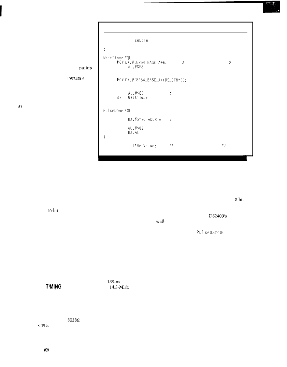
transaction starts from the same
known state.
In general, the PC will read the
serial number only once during its
power-on reset sequence. The DS2400
has no power dissipation specification,
but leaving the signal line high at the
end of the transaction eliminates the
few milliwatts dissipated in the
resistor...which is surely orders of
magnitude more than the
Figure 3 details the five wave-
forms needed for the DS2400 interface.
The reset pulse is easy, because it has
only minimum times: no less than 480
for both the low and high parts. The
transmit and receive pulses are more
critical because they are only a few
microseconds long and the PC must
accurately measure the received pulses
to decide what they are.
When a project’s timing is de-
nominated in microseconds and you’re
charged with writing the pulse
measurement code, get ready for some
serious thinking! The first question is
whether it’s even possible, and if you
decide it is then the next question is
what’s the best way to pull it off.
As an aside, sometimes you really
will be asked to do the impossible.
One recent BBS thread involved a
project that was supposed to sample an
analog voltage at something like 20
MHz and store
values direct to
disk using a custom PC ISA bus card.
If you’ve been paying attention to
this series, you know that can’t
possibly work (why?) but the require-
ment was proposed in all seriousness.
My advice was to present the ISA bus
limits, then hide behind a bush if the
project continued in defiance of
reality.
Fortunately, it was canned when
the engineer explained how the PC
world was really put together....
HARDWARE
If you use the DS2400 in an 805 1
microcontroller system you can
determine pulse widths by simply
counting instruction cycles and
writing a timing loop with a known
duration. Not so with the
In
fact, 80x86
encourage program-
ming as an experimental science:
figure out how long a loop should last,
Listing l-continued
J M P P u l
wait for timer interval to expire
*
latch read back counter status
MOV
OUT DX,AL
read counter status
IN
AL,DX
TEST
wait for it to go high again
RET
*
MOV
IN
AL,DX
XOR
OUT
clear sync pu lse
return
return Boolean value
write it, measure the results, then
tweak the loop count to make the
answer come out right. With any luck,
a few iterations will converge on the
desired value.
If your luck goes the other way,
though, changing PC board vendors,
moving the program from RAM to
EPROM, or just twiddling a few BIOS
setup values will clobber your
tuned loop. Some of the tricks you use
routinely in 8051 code just don’t apply
anymore: delay loops are in the “better
to avoid if at all possible” category,
although 1’11 show you a good use for
one a little later on.
The 8254 timer chip on the
Firmware Development Board was
intended for just such applications: it
can measure time intervals up to 9 ms
with
resolution. It’s connected
to the
clock, so the time
intervals do not depend on the CPU’s
clock frequency or system board
hardware, which means you’ll get the
same results every time.
Remember, however, that there
are some limitations. If you are trying
this on an old 8088 system, it may not
execute fast enough to keep up with
the short intervals produced by the
8254. The pulses will be timed by a
single pass through the timer code
because the hardware will be ready
long before the code checks it. On the
other hand, the Firmware Develop-
ment Board won’t work in an
ISA
slot, so you’ll have a few other prob-
lems before getting to the time delays.
Because the
read and
write pulses are so similar, I combined
the code into the routine shown in
Listing 1.
is written in
8086 assembler in a Micro-C wrapper,
so the input arguments and local
variables are on the stack rather than
static storage locations.
Although the 8254 timers can
produce hardware interrupts, I use
simple software polling to detect the
end of each pulse. Remember that
hardware interrupt handlers must start
by saving the CPU registers and
setting up the segment registers. When
you are dealing with microsecond
pulses, that takes far too long.
There are sneaky ways to stream-
line hardware interrupt handlers under
very special, carefully controlled,
conditions, but 1’11 save those for a
later column. You’ve seen some of the
tricks already: the key is to know
52
Issue October 1993
The Computer Applications Journal
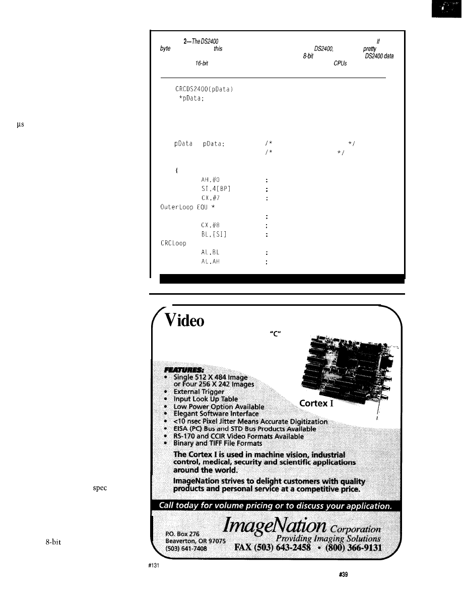
exactly when the handler will be
active so you can preload the registers.
The DS2400 didn’t call for such
gymnastics, so I could get away with
polling. Whew!
The first timing loop measures the
low part of the pulse. If the mainline
code is writing a zero bit, this will last
for 90 us, but when it is reading data
from the DS2400, the pulse is only 5
long.
Pul seDS2400
also sets a sync
bit in the parallel printer port to mark
its entry into this code; if that bit
never goes low again, you know you
have hardware problems on the
Firmware Development Board. If you
plug in the LED-and-switch box I
described in Issue 3 1, you can watch
the firmware in action, which is often
reassuring.
The 8254 output pin goes low
during the pulse and returns high at
the end. The delay loops load the timer
count registers to start the interval,
then poll the output status bit. Polling
involves writing a latch command to
the 8254 and reading the status
register, so it’s slower than a pure
input bit. A 33-MHz ‘386SX is fast
enough that this doesn’t add too much
delay, but if time were really critical
you could route the timer output bit
back through an input port to poll it
directly.
After the low-pulse time ends, the
code writes a one to the DS2400
output bit and sets a two-microsecond
delay. When that interval expires, the
code samples the DS2400 input bit and
records the value; if this is a read
pulse, the DS2400 controls the signal
line. For bits written from the PC, the
sampled value is simply ignored.
Following the sample, the code
loads the timer with the rest of the
required high time plus the mandatory
one-microsecond idle time and waits
for it to expire. Because the DS2400
output is now high, additional delays
are OK, so the code also enables
interrupts. The DS2400
sets the
minimum idle time, but does not
specify a maximum so a protracted
delay will not cause a data error.
The code this month includes
routines that use
Pul seDS2400 to
write the
command word (always
OF) and read back all 64 bits from the
Listing
includes an d-bit CRC computed over its Type ID and serial number data. the
you compute using
algorithm matches the one read from the
the odds are
good that
no errors occurred during the transfer. This code is based on the
algorithm shown in the
sheet, but uses
registers to shuffle the bits because the 8051 and 80x86
do no set the ALU
flags in the same way.
int
BYTE
int CRC:
=
keep compiler happy
CRC = 0:
clear both bytes
asm
MOV
MOV
MOV
PUSH CX
MOV
MOV
EQU *
MOV
XOR
set up initial CRC
set up data pointer
set up byte counter
save byte counter
set up bit counter
fetch data byte
set up data byte
combine low bit with old CRC
(continued)
Frame Grabber
l
$495 Including Software with
Library
l
Half Slot Card for Compact Applications
l
Real Time Imaging with Display Output
l
8 Bit (256 Gray Levels)
The Computer Applications Journal
Issue
October 1993
5 3
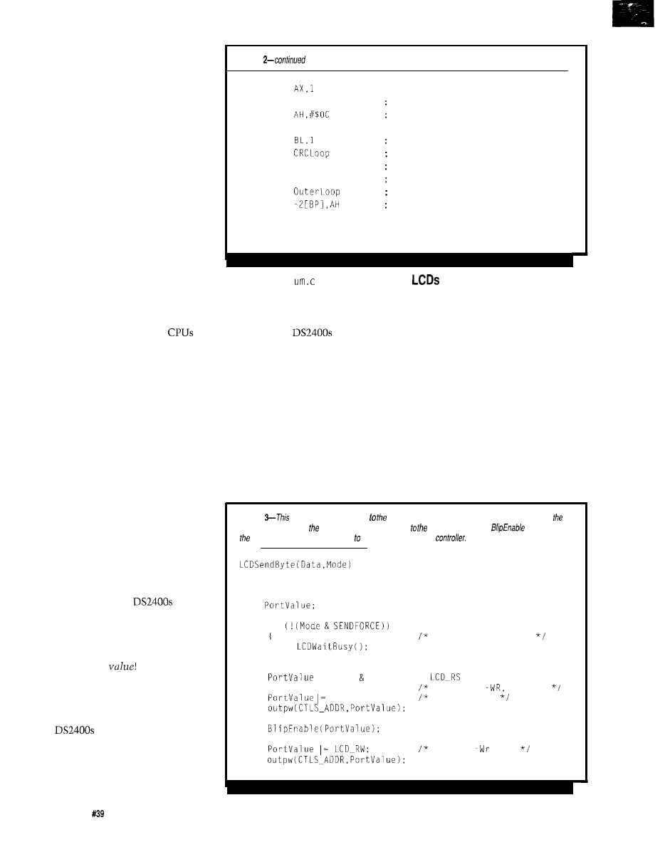
DS2400. It’s quite straightforward,
except for one little, teeny, tiny detail:
you must transmit and receive bytes
low-order bit first. Believe it or not,
that critical fact isn’t mentioned
anywhere in the data sheet!
CHECKING YOUR ID
Once you read the DS2400 data,
you should verify that it is correct by
using the CRC byte. You may, if you
like, assume that nothing can go
wrnog (oops!) with such a simple
interface, but I’d suggest checking the
CRC value just to be sure. The CRC is
computed over the Type ID byte
(which is always 01) and the six bytes
of data.
The DS2400 data sheet presents
the CRC algorithm as an 8051 assem-
bler subroutine. It’s tempting to just
transliterate it into 8086 assembler,
but there’s a gotcha: the two
set
the flags differently for some ALU
operations, so a simple line-for-line
conversion won’t work. Listing 2
shows the 8086 code I use to compute
the CRC; it takes advantage of the fact
that we can handle 16-bit values with
no extra effort.
Just when you think you’ve got
everything right, though, there’s a
gotcha lying in wait. I recall a BBS
thread from some years back where
somebody simply could not get the
right CRC value. They were using the
Dallas algorithm on an 8051 CPU, so
there was no question of a translation
error, but the CRC byte read from
their DS2400 chips simply did not
match their computed values.
After considerable headscratching
and many calls to Dallas’ tech support,
they found that their
were
wrong! There was a little glitch in the
code driving the production line laser:
it burned a unique serial number into
the chip, then computed and burned
the wrong
CRC
Talk about
hard-to-find bugs....
Needless to say, that was fixed
PDQ so all current DS2400 chips are
OK. However, if you have a stash of
old
check them very carefully
just to be sure....
I’ve said it before and I’ll say it
again: hell hath no fury like that of an
unjustified assumption!
Listing
ROR
JNC
XOR
Zero EQU *
SHR
LOOP
INC
POP
LOOP
MOV
Zero
SI
cx
return CRC;
; put result into high bit of CRC
and into carry flag, too
stir in preshifted constant factor
set up next data bit
repeat for all bits
aim at next byte
fetch byte counter
and repeat for each byte
set up return value
The se r n
program available
on the BBS reads back the DS2400
data, calculates the expected
checksum, and displays everything. To
judge from the
I have on
hand, Dallas produced about 400,000
parts before I bought these, at least if
they’re assigning the serial numbers
sequentially.
If your circuit doesn’t work the
first time, se r
n
um also writes the
command byte in a tight loop so you
can scope the DS2400 data pin to see
what the trouble may be. The circuit is
simple enough that a solder splash
should be the extent of your troubles,
but you never can tell....
REDUX
The Firmware Development Board
sports a pair of seven-segment LED
digits that we’ve used to report error
conditions and display status informa-
tion. The messages tend to be cryptic,
but for our purposes they suffice. If
you want to dress your system up for
company, though, you need at least a
smidgen of legible text output. The
small LCD panels we’ve used on 805 1
systems are equally handy on PCs; it’s
a simple matter of firmware to get one
working.
Back in Issue 8 I did an in-depth
review of these displays, so I’ll refer
you there for the details of how they
Listing
code writes a sing/e byte LCD pane/. The Mode argument determines whether
byte is a character for display buffer or a command LCD controller. The
routine pulses
LCD’s Enable input high and low strobe the byfe into fhe
WORD Data;
WORD Mode:
WORD
if
force without wait?
= (Mode SENDDATA) ?
: 0;
cmd/data,
enabled
Data:
combine data
disable
line
5 4
Issue
October 1993
The Computer Applications Journal

work and what all the interface lines
mean. For now, I’ll concentrate on the
specifics of the Firmware Develop-
ment Board’s application.
The common denominator of all
these panels is the Hitachi HD44780
LCD controller that provides their
(admittedly limited) intelligence. Most
of the character LCD panels you’ll find
use this controller, but it’s a good idea
to get the data sheets along with the
hardware just in case you wind up
with an oddball. Drop a note on the
Circuit Cellar BBS and we can prob-
ably walk you through getting your
display working.
The code this month can handle
any HD44780 display up to the
maximum of 80 characters; it arrives
set for four lines of twenty characters.
A pair of constants define the number
of visible rows and columns so, after
changing two lines and recompiling,
you’re up with your new display.
As shown in Figure 1, the LCD
panel interface uses port I/O rather
than a direct PC ISA bus connection.
Although a bit-banged interface is
considerably slower than a bus
hookup, the firmware can still update
the entire display faster than the liquid
crystals can respond. So that’s prob-
ably fast enough.
Listing 3 shows the few lines of
code required to write a byte to the
display. The LCD’s Enable line latches
the data into the controller, so the
code writes the 16-bit port three times:
once to set up the data and control
lines with Enable low, once to set
Enable high, and a final write to lower
Enable.
Because the port’s data cannot be
read back into the CPU, the code holds
them in the
P
O
r t V a
1 u e
variable
between writes. This simple trick
suffices for now, but I’ll describe some
of the problems that can arise in
world code after we get the LCD panel
on the air.
Listing 4 is the routine that reads
status and data from the LCD control-
ler. This code is used in two places: to
check the controller’s (Busy) status flag
before sending a new command or data
byte and to read the display buffer
during vertical scrolling. Both of these
functions can be simulated in
T
HE
I
N C R E D I B L E
N
E W
PE-8351 FX
I
N
- C
IRCUIT
E
M U L A T O R
$1451.00
n
supports
Other Fine Emulators
New Debugger
8X52/32,
From
Enhancements
Real-time and Nonintrusive
n
68HCt
n
Full support for structures,
n
64K Program Memory
n
68HCO5 From
unions, arrays, pointers
64K Data Memory
n
COP8 From
n
Data structure
n
128K Hardware Breakpoints
n
More than 100 devices
browser/editor
Frame Trace Buffer
supported through
n
True expression in watch
n
Transparent Trace
changeable probe cards
window-detect bad pointers
(View Trace and Execute
Simultaneously)
Nobody Matches the Value of the PE Family
PE Product
M a x
n
Fast, Easy Installation to
list
List Price*+
RS232 Port of any D
OS
P C ,
8351 FX
1 6
$ 1 4 5 1
$4820
even Laptops!
8 3 7 5 1 1 7 5 2 1 6
4300
n
Built-in Self-Test
8032-24 24
8 5 1
4945
8032-42 42
999
7 1 9 5
n
Symbolic Debug
‘U.S.
Retail price.
‘U.S. Price
List dated
verbal
n
Source-Level Debug
Our new AET Emulator
architecture
(Advanced Emulator Technology, Pat. Pending)
providesunmatchedvalue.
including
money backguarantee, 10
periods, rental
free technical support. Call
for
FREE
demo diskette
Corporation
325 E. Elliot Road, Chandler, A
Z
8 5 2 2 5
Phone: (602) 926-0797 Fax: (602) 926-l 198
Europe
2,
(08091) 2046, Telefax (08091) 2386
See us at Embedded Systems Booths
325
The Computer Applications Journal
Issue
October 1993
5 5
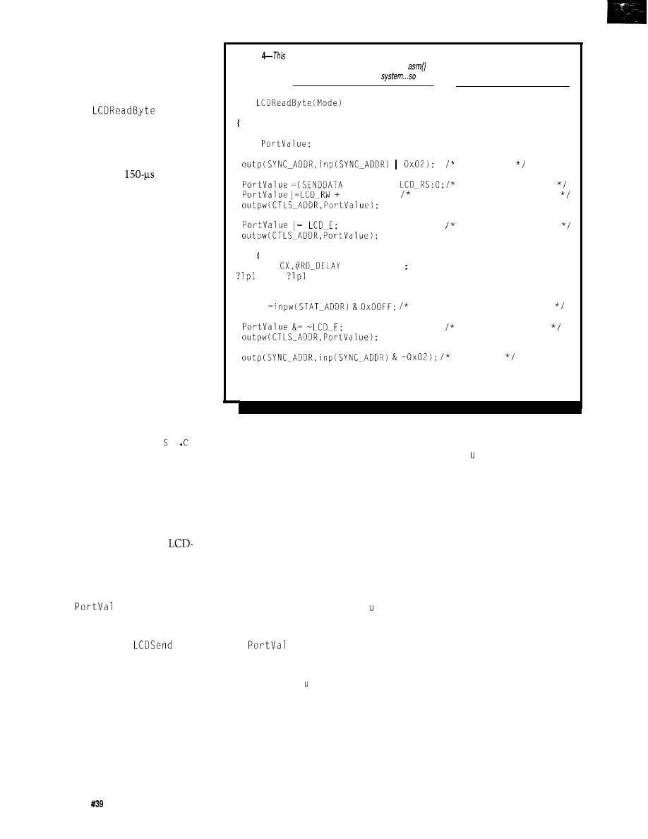
ware, but at the cost of one ‘245 buffer.
I decided to use Steve’s favorite
programming language: solder.
Despite my tirade about software
delay loops, you’ll find one buried in
the heart of
just after
the code raises the Enable line. Some
of the LCD panels I’ve used need more
time to drive data back to the Firm-
ware Development Board. The value I
settled on creates a
pause that
is about four times the delay my worst
panel needs, but if you get erratic
vertical scrolling, you’ll know what
the problem is and where to fix it.
This may be related to the ribbon
cable layout that comes naturally to
these panels, although I don’t see a
glitch on the scope. You might want to
experiment with different cable
layouts to see if bracketing the LCD’s
Enable or the data lines with pairs of
quiet ground lines helps. Trust me on
this: if you haven’t used firmware to
fix hardware before, it’s time you got
started....
The remaining LCD code adds
cursor positioning, string output,
simple scrolling and some control
character processing. It’s straightfor-
ward code available on the BBS if
you’re interested. The
1 cd t e t
program provides several test loops
with scope triggers, as well as a
routine that copies incoming serial
characters to the LCD so you can
check displays out by hand.
Extra credit project: you can add
ANSI cursor positioning support fairly
easily. The description of the
Link project in Issue 27 should get you
started.
SHARED BITS
The
ue
variable let
LC D S e
n d By t e
toggle the LCD Enable
line while holding all the other bits
steady. Unfortunately,
Byt e
has no way to preserve the existing
bits because the port can’t be read
back. That has no effect on the
demonstration program, but in real life
it’s a killer problem.
For example, the watchdog timer
routines I discussed in the last column
send a new bit to the watchdog about
six times a second. That interrupt
handler cannot read back the existing
Listing
routine
reads a byte from the LCD controller; the Mode argument determines whether it comes
from the display buffer or the controller. The loop in the
section compensates for delays caused by
cable capacitance and must be tuned for each
there is no need for a precise measurement.
int
WORD Mode:
WORD Data;
WORD
scope sync
== Mode) ?
read data or addr?
LCD_NODRV; LCD rd. and disable drivers
strobe data fr. LCD
asm
MOV
LOOP
delay allows data settle time
Data
fetch and isolate LCD data
remove LCD strobe
sync off
return Data:
bits, so if you are writing a byte to the
LCD controller, it will clobber your
data while toggling the watchdog.
When the LCD write completes, it
returns the favor by clearing the
watchdog bit.
This problem is easy to solve in a
single program: all your routines must
use a single global P o
r t V a 1 u e
variable
to hold the current state of the output
port. If an interrupt handler can change
the port, you must protect your
noninterruptable code by disabling and
enabling interrupts around the sec-
tions where you twiddle P o
r t V a 1 e.
An oversight here can cause some
subtle bugs. When your mainline code
loads
ue
into a register to
change the bits, as most C compilers
will, your interrupt handler can get the
“old” P o
r t V a 1 e
from the variable,
change a few other bits, and write it
back; your mainline code will then
destroy the handler’s bits when it
writes its P
O
r t V a 1 ue
back into the
variable.
It’s worth working through a few
examples on paper to convince
yourself that you’re in a lot of trouble.
Look for those instants in time when
P o
r t V a 1 e
differs from the actual port
bits: that’s when the interrupt handler
will strike. Then make sure only one
routine can alter P 0
r t V a 1 u e at any
time and always keep the variable in
sync with the hardware port.
I’ll be working through these
issues in the next few months, but I
figured I should at least point out the
land mine right now. This problem is
known and the solutions are docu-
mented in the multitasking literature.
You’ve surely read about semaphores,
critical regions, atomic locking, and
threads of execution by now; if not,
well, back to the books.
RELEASE NOTES
The downloadable code this
month has two Micro-C programs that
exercise the DS2400 and LCD panels.
You can combine the routines, but pay
attention to the “shared bits” problem
described above. If you stir in the
watchdog code from the previous
issue, it gets still more complex!
5 6
Issue
October 1993
The Computer Applications Journal

If you don’t like the notion of a
serial-numbered PC, you’re in good
company. But if you’re writing code
that must know for sure that it’s
running on authorized hardware, now
you’ve got a good idea of how to start.
I’ll leave the encryption and hacker
defenses to other writers, but will
make use of the serial number in a few
dangerous projects.
If serial numbers really annoy you,
though, I’m sure The Great Dybowski
can come up with an 805 1 -based
DS2400 emulator to produce any serial
number you like with the push of a
button...and I might even help him
out!
Next month: despite my best
intentions, I’m going to talk about
embedding an entire Micro-C program
as a BIOS extension. You can’t fit too
much into
but sometimes a little
code is better than none at all.
q
Ed Nisley, as Nisley Micro Engineer-
ing, makes small computers do
amazing things. He’s also a member of
the Computer Applications
engineering staff. You may reach him
on CompuServe at
or
through the Circuit Cellar BBS.
DS2400 Silicon Serial Numbers
are available from the usual
order suppliers. LCD panels based
on the Hitachi HD44780 control-
ler make frequent appearances in
electronic surplus catalogs, so you
can save quite a bit of money if
you need just one or two. Check
the supplier listing in the Febru-
ary 93 column for suggestions.
Pure Unobtainium has the
complete Firmware Development
Board schematic, as well as
selected parts. Write for a catalog:
Pure Unobtainium
13 109 Old Creedmoor Rd.
Raleigh, NC 276 13
Phone/fax: (9 19) 676-4525
410
Very Useful
411 Moderately Useful
412 Not Useful
What
IS
C thru ROM?
ROM
Your Borland
or
Microsoft
is the complete ROM development software tool kii.
tt lets you run Microsoft and Borland C and C++ programs on an
embedded 80x86 CPU without using DOS or a BIOS.
you money. There
no DOS or BIOS royalties
to pay for your embedded systems.
is complete! It includes the following and much more:
*Supports Borland’s Turbo Debugger.
*Remote Code View style source level debugger.
startup code brings CPU up from cold boot.
library in source code.
*Flexible 80x86 Locator.
PACKAGE
MONEY
The Computer Applications Journal
Issue
October
1993
5 7

HCS
Jeff Bachiochi
interface, and program storage. A
piggyback-style expansion bus offers
I/O interfacing and plenty of
ing area.
This approach reuses a
stone building block (80% of the
Add the Touchtone Interactive
circuit) leaving only the untested bits
Monitor to you
control system
home
ardware for the
interface has taken
an unexpected detour.
The original plan for adding the
telephone interface link to the existing
HCS network was unexpectedly
canceled. Stay calm now, I said the
orginal plan was canceled, not the new
plan. Let me explain.
Production boards for the HCS II’s
network links are single-board layouts
of prototyped hardware. Prototyping a
new I/O link is easy because only the
new I/O circuitry in question needs to
be built. Although the production
board is a single-board layout, to lower
of silicon to be manually connected.
The intake of tin/lead/flux fumes is
therefore kept to a minimum.
(Wouldn’t it be nice if someone would
produce flux in different fragrances.
Anyone willing to invest in such a
venture?) This shortcut allows you to
quickly get down to the software
necessary to make the hardware jump
through the proverbial hoop.
INITIALLY, A SIMPLE CONCEPT
As with the other HCS link
modules, the telephone interface
would talk to the Supervisory Control-
ler through the twisted-pair network.
The hardware should allow a connec-
tion to be established between the
pair and the telephone link
interface board.
It all starts with a legal connection
to the phone system allowing the HCS
to monitor the phone line, answer a
ring, and recognize and produce DTMF
signals. In addition, the appropriate
circuitry for injecting and retrieving
Photo
ifs new
telephone
the HCS can originate
or receive calls and in
cases allows
homeowner interact
system remotely.
58
Issue
October 1993
The Computer Applications Journal

on the
board centers around
the
chip. The supporting cast of components includes
DAA chip and
some glue logic.
other audio offers some additional
benefits. And what network link
would be complete without some
high-voltage I/O: just a few
inputs and a modest offering of
collector outputs. The schematic for
the newest member of the RTC/HCS
family is shown in Figure 1.
whole electronics industry I don’t
the only name you have found. In the
know of another market in which
competition seems to disappear so
silently.
To comply with Part 68 your
circuitry must:
DAA
*Prevent supplying currents greater
than 10
and voltages greater
than 70 volts to the telco line.
*Limit strength of transmitted signals
between 100 Hz and 1 MHz.
*Not create an imbalance between the
two telco connections (tip and ring]
and ground.
you may then submit an application to
the Federal Communications Commis-
tests, the device continues to comply,
sion. Proving compliance is best left
up to FCC testing laboratories. For a
fee, starting at about $1500, they will
test your device and suggest changes
necessary to bring it into compliance.
They will submit the proper paper-
work, on your behalf, to the FCC.
The FCC requires that any device
connected to telco equipment conform
to basic safety standards (Part 68)
protecting both telco and the con-
sumer. Of course, you must prove you
comply, or you can use a preapproved
front end or DAA (direct access
arrangement).
are not overly
complex, nor are they inexpensive,
which doesn’t seem to make sense. If
you’ve ever looked for a DAA, you will
most certainly have come across the
name Cermetek. In fact, it is probably
*Limit both “on hook” (DC] and “off
hook” (AC or ringer) impedance.
*Provide protection against service
theft.
If, after severe electrical surge,
vibration, temperature, and humidity
The Cermetek CH1840 complies
with all requirements for voice and
data use through V.32. It is Part 68
tested and registered. This registration
is passed on to the user as long as
simple trace and isolation criteria are
obeyed.
Refer to Figure 2 for a block
diagram of the CH1840. This DAA
requires only volts, which goes a
long way toward simplifying the power
supply design. Only two signals are
necessary for telco connection. The
The Computer Applications Journal
Issue
October 1993
5 9

Balance
Hazardous Voltage And Current
TIP
RING
Figure
preregistered DAA provides a
interface to the telephone line. It connects audio to the
tip
and ring lines plus provides ring
and off-hook control. An optional forced billing delay a/so
with
regulations.
Tip and Ring signals (named after parts
of the phone jacks used to manually
connect customers on the first tele-
phone switchboards) carry both
incoming and outgoing audio. These
signals are not referenced to ground.
All remaining signals are user connec-
tions. The
and Xmit connections
are ground referenced and provide the
user with separated audio in and out.
*Data/Voice and Offhk inputs enable
the billing delay and take the line off
hook. *RI and Psq outputs indicate the
presence of a ring signal and a squelch
of the audio input.
DTMF
One of the first transmissions of
data in a digital format was the
telegraph. Dots and dashes (zeros and
ones) are grouped to represent alphanu-
meric characters. Today we are all too
t o n e
Low
tone
697Hz
1209 Hz
1
697Hz
2
697Hz
3
697 Hz
A
770 Hz
4
770 Hz
5
770 Hz
6
B
852Hz
7
852Hz
1336Hz
8
852Hz
9
852Hz
1633 Hz
C
941 Hz
1209 Hz
0
941 Hz
1336 Hz
l
941 Hz
941 Hz
1633 Hz
D
Tablel-Each
16
is
made up of a pair of tones.
familiar with sounds of modem or fax
conversations, especially when
connecting with one unexpectedly.
Telephones based on dual tone,
multifrequency (DTMF), also known
by the trademarked name Touch Tone,
are rapidly replacing the old rotary dial
telephones. This is allowing central
offices to upgrade to electronic
switching equipment. The advantages
of an electronic system over a mostly
mechanical one are many: power
savings, increased MTBF, and flexibil-
ity just to name a few. It’s easy to see
why these advancements were eagerly
(read “slowly”) embraced by the phone
company.
DTMF tones are triggered by a
matrix of four columns (three columns
on your telephone) by four rows that
can produce sixteen (twelve on your
phone) possible key positions. Each
column and each row has a different
tone assigned to it, giving sixteen
(twelve) distinct tone pairs. Each key
combines the appropriate row and
column tones. In this fashion, sixteen
possible combinations (a nybble of
information) can be passed at one time
using only eight discrete frequencies.
The eight tones were carefully
selected to fit within the narrow
of the telephone system
and so the tone harmonics would fall
between other tones so as not to cause
a false image. See Table
1
for the valid
tone-pair combinations.
Notice the digits A-D are not on
your phone, however these are legal
DTMF codes and can be both
nized and produced by existing DTMF
circuitry. The ability to receive and
transmit DTMF is not always needed
in many products, but when it is, one
of the most widely chosen
is the
M8880 (from Teltone, Mitel, and
others). Since the
is specifically
designed to interface with a 6800
series microprocessor, it doesn’t
interface easily to 803
1
-style architec-
ture, the one used on the RTC3
1.
Sometimes manufacturers do
listen to designers though, because the
M8880 has mutated just this year into
the M8888. Same core, but now can be
directly interfaced “Intel style.”
DTMF tones are produced by writing a
nybble to the
data register.
Recognized codes are reported in the
same nybble format. An interrupt pin
can flag completion of an event
(sending or receiving a DTMF signal)
or a status register can be polled for
this information. The M8888 will
produce DTMF signals with the proper
duration and spacing as well as reject
incoming tones which do not fall
within acceptable limits. All this
integration makes DTMF a snap. It is
the call progress interpretation which
will cause the headaches. For a look at
the level of functionality this chip
brings to the table, have a look at
Figure 3.
Call progress tones fall into a
separate
of
Hz. The
call progress mode switches
in a special
filter which
passes only these signals to the
l
IRQ
pin. It is left up to the user to deter-
mine the state of the call from this
signal. See Table 2 for typical call
progress signals.
If you look closely at the frequen-
cies and durations, you will see that
there are actually two ways of distin-
guishing between call progress tones.
By comparing On/Off timings and by
determining frequency content. See
the scope shots in Photos
for
signal comparisons.
AUDIO
Up to this point, everyone at
Circuit Cellar had pushed the HCS
telephone interface in the same
direction. Although we all agreed voice
response is necessary, tempers flew to
60
Issue October 1993
The Computer Applications Journal

new heights when-
ever the interface
topic turned to
speech.
Digitally
recorded speech is
hot right now. New
compression meth-
ods are popping up
everywhere. Every-
one seems to have
their favorite, and
they’re willing to
defend it to great
limits and with
considerable zeal.
No matter what
the algorithm, some
facts can’t be
C o l u m n
D a t a
Counters
Bus
Buffer
RSO
Figure
transceiver takes care of the details
for receiving and generating
also provides
limited
progress information for
processing by the host computer.
ignored. To store large vocabularies,
So where does this leave us!
memory or recording hardware. The
digital speech requires lots of memory.
Speechless? Not exactly. Early speech
disadvantage was that it would
It also requires extra hardware to
synthesizers were based on the or
produce almost unintelligible speech.
record, edit, and store the phrases.
so phonemes (sounds) that all words
Speech quality has improved since
Canned speech severely limits the
are composed of. Text-to-speech
then; more processing power has
potential responses you may wish to
firmware dissected each word into
helped create smarter algorithms.
give. Think of all the possibilities just
reproducible phonemes. The big
Exception tables help pronounce even
to say, “The outside temperature is x
advantage here was unlimited
the screwiest of English words
degrees.”
without the need for banks of
Project Part5
UPS
day
to
48
US states. COD add $4.50. Canada $6
via USPS
Small
Packet, no
Check, MO,
COD only, no
cards.
add $50. but
NC
add 6% sales tax
at
parts Data Sheets Included.
Call/write/fax for seriously tempting catalog...
Pure Unobtainium
unusual
13109 Old Creedmoor Road Raleigh, NC 27613
FAX/voice (919) 676-4525
The BCC52 controller continues to be
Micromint’s best selling single-board com-
puter. Its cost-effective architecture needs
only a power supply and terminal to become
a complete development system or
board solution in an end-use system. The
BCC52 is programmable in BASIC-52, (a
fast, full floating point interpreted BASIC), or
assembly language.
The BCC52 contains five RAM/ROM
sockets, an “intelligent” 27641126 EPROM
programmer, three
parallel ports, an
auto-baud rate detect serial console port, a serial printer port, and much more.
PROCESSOR
CMOS processor w/BASIC-52
Console
detect
parallel
EXPANDABLE1
B C C 5 2
Controller board
BASIC 52 and RAM
$189.00
Low-power CMOS
of
BCC52
$ 1 9 9 . 0 0
-40%
industrial temperature version
$ 2 9 4 . 0 0
Low-power CMOS, expanded BCC52
RAM
$ 2 5 9 . 0 0
CALL FOR OEM PRICING
INC.
(44)
Canada:
Welcome!
The Computer Applications Journal
Issue
October 1993
6 1
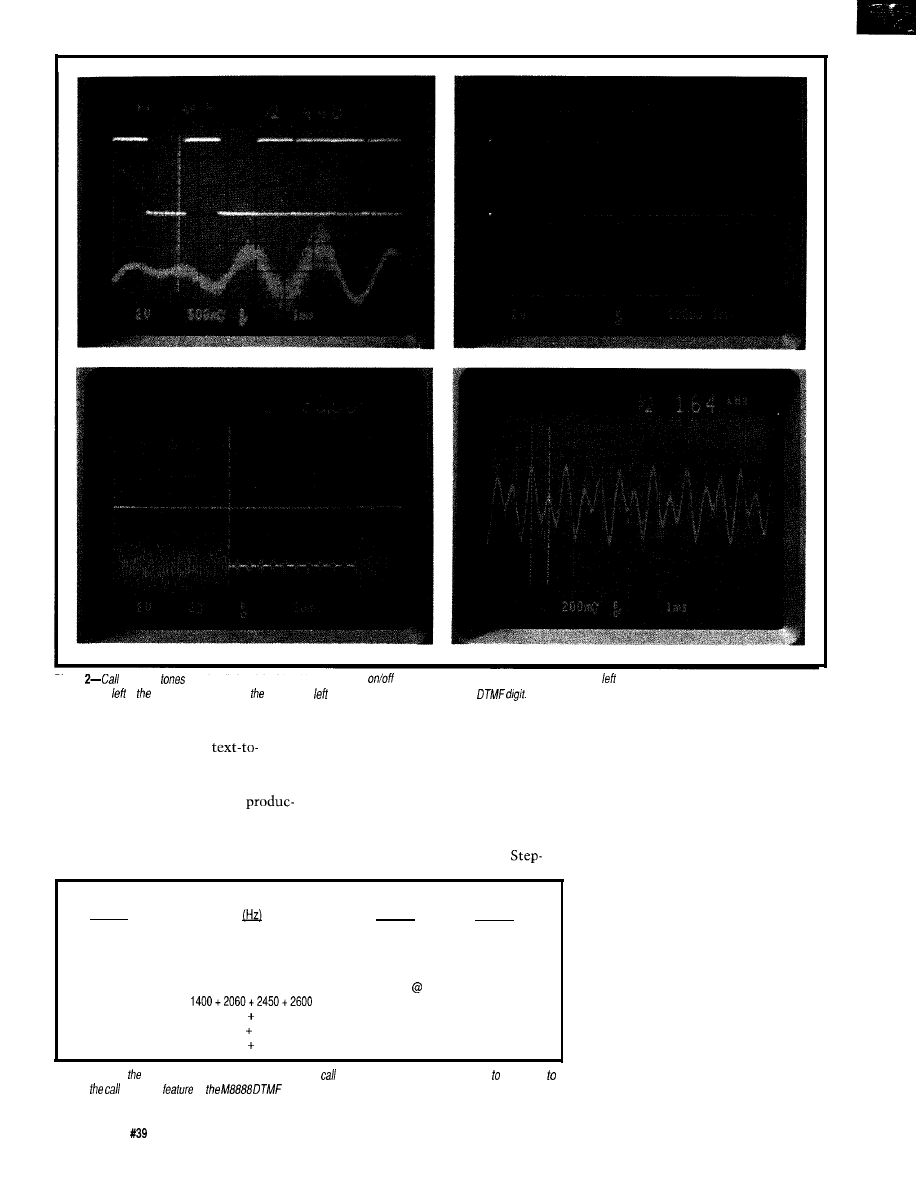
Photo
progress
can
be distinguished by either comparing
timings or finding frequency content The upper
screen shows a dial tone, upper right is a busy
signal, lower is signal produced when receiver is off hook, and lower righf shows a
After evaluating many forms of
When the circuitry for the DTMF
speech reproduction, the
interface is combined with the speech
speech approach won hands down due
synthesizer, the processor, and
to its reasonable cost and flexibility in
network communications, the single
our application. To help speed
link board size expands beyond what
tion, we chose to license the firmware
we thought was practical for a network
but lay out the circuitry on another
RTC expansion board.
node. This implementation was
beginning to exceed optimum.
Function
Dial
Busy
Ring Back
Frequency
350 + 440
480 + 620
440 + 480
No Such Number
Left Off Hook
Congestion
Reorder
Ring Back PBX
200 to 400
480 620
80 620
440 480
On Time
[seconds)
continuous
0.5
2
Off Time
(seconds)
0.5
4
continuous FM 1 Hz
0.1
0.1
0.2
0.3
0.3
0.2
1
3
Table
P-Knowing frequencies and cadences used by typical
progress signals is necessary write code
I couldn’t be happier. Not only
support
progress
of
transceiver.
does the HCS get its telephone
ping back far enough for a look at the
forest gave all of us the insight
necessary to see the trees in a different
light. Why bog down the network with
text and dialing strings when a better
solution was staring back from the
prototyped interface? The RTC
expansion headers designed into the
8031 board I used to test these
prototypes were also part of the HCS
Supervisory Controller. A separate
link was not necessary. The HCS can
handle these two boards (DTMF and
speech) directly. All heads turned to
Ken, “It can, can’t it?” A pause of the
appropriate length was inserted here to
provide just the right amount of
suspense. “Makes sense to me,” was
the answer we all wanted to hear.
6 4
issue
October 1993
The Computer Applications Journal

interface, but get a couple of new
expansion boards I can use with my
RTC boards.
TYPICAL HCS CONVERSATION
Ringggg...
“Hello,
Circuit Cellar INK.”
“This is the HCS II calling for Jeff
Bachiochi. Jeff, please enter your
digit access code.”
<hold pressed>
<extension called>
“Jeff, some machine is asking for
you on line 12”
“Thanks, Nancy!”
<line picked
bip
tones entered>
“Jeff, I know you plan to be home
soon, would you like me to turn on the
air conditioning for you? It is 82
degrees in the family room.”
bleep
pressed>
“It is now after 3:00
P
.
M
.
The
security system is still active. No one
has entered the premises since it was
activated at
A
.
M
.
am worried
about the children. Do you have any
additional commands for me?”
bleepity-bloopity-blump <Touch
Tone sequence pressed>
I don’t want to find out how can save a lot of money using
ROM-DOS 5 instead of MS-DOS@ in our 80x86 product line.
I don’t care if ROM-DOS 5 iscompatible with MS-DOS 5 but
costs much less. I like spending much more than I have to.
It makes me feel like a philanthropist and besides Microsoft@
,
probably needs the money more than I do anyway.
3
es,
I want to know the facts about ROM-DOS 5.
Please send me information and a free bootable demo disk to
try with my software.
CCI-10193
In
the U.S.A. Call Toll Free
or
fax this coupon to (206)
I
Name
Company
Address
Phone
State
Fax
“I understand. Record channel 4 at
8:00
P
.
M
.
for 1 hour. Do you have any
additional commands for me?”
bleep
pressed>
“Don’t worry. I have everything
under control. Goodbye.”
<called ended>
“Who was that?” questioned
Nancy, our receptionist.
“Oh, just my house checking in. I
forgot to tell it we were all going out
to celebrate our anniversary tonight!
It was just following orders.” 1 grinned
at her sheepishly as I left for the
evening. It felt good to know that
someone was watching the house
while I was out. Now, did I remember
to tell the HCS where I could be
reached tonight?
q
Jeff Bachiochi (pronounced
AH-key”) is an electrical engineer on
the Computer Applications
engineering
staff.
His background
includes product design and manufac-
turing.
Cermetek Microelectronics
1308 Borregas Ave.
Sunnyvale, CA 94089
(408) 752-5000
Teltone Corp.
Ave. SE
Bothell, WA 98021
(206)
Mite1 Semiconductor
2321 Morena Blvd., Ste. M
San Diego, CA 92110
(619) 276-3421
HCS II DTMF Telephone Interface
(RTC-DTMF) kit or assembled
HCS II Text-to-Speech Interface
(RTC-Voice) assembled only
Contact Circuit Cellar Inc., 4 Park
St., Vernon, CT 06066, (203)
8752751 for more information.
413
Very Useful
414 Moderately Useful
415 Not Useful
RS-DOS
trademarks
Corporation
36
The Computer Applications Journal
Issue
October 1993
6 5
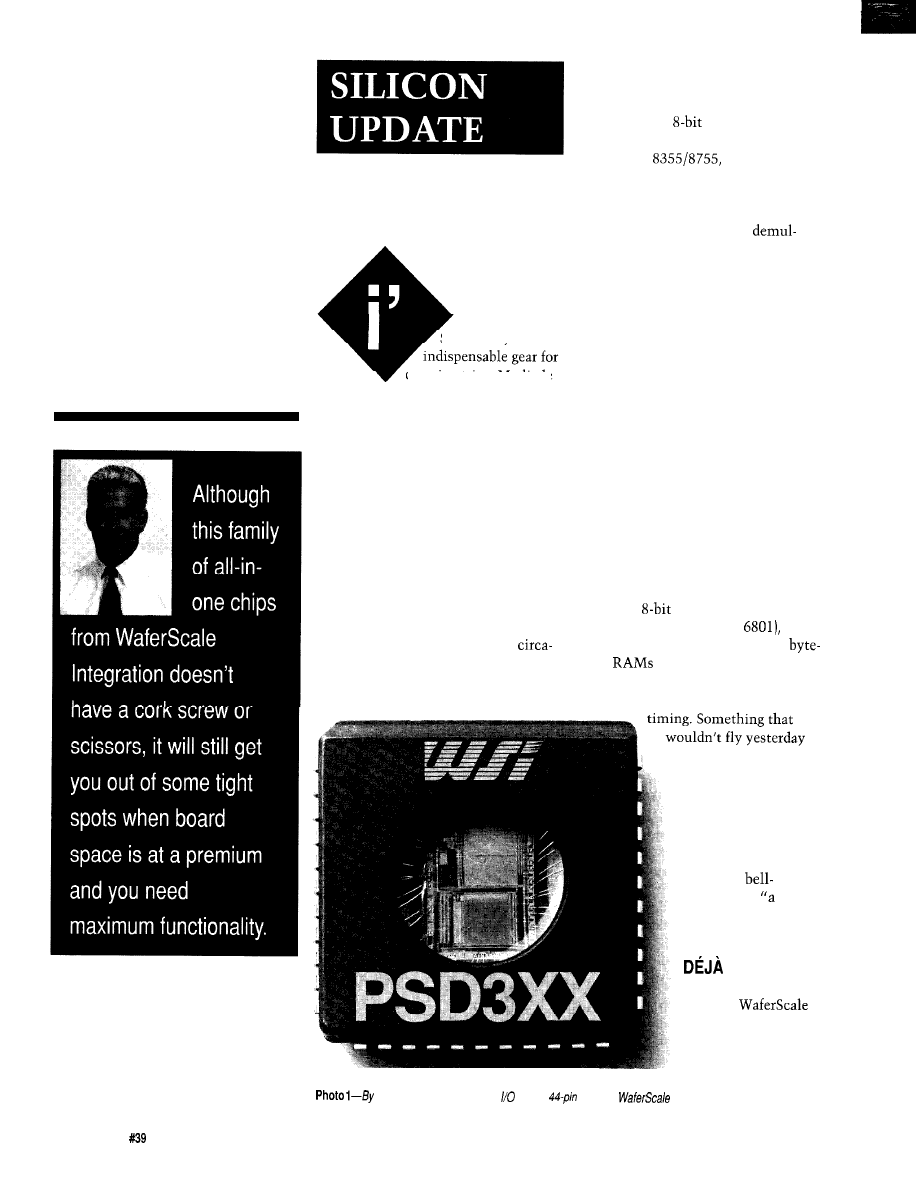
Swiss
Army Chip
Tom Cantrell
ve found that a
Swiss army knife is
camping trips. My little
red gadget has proven to be a life saver
on more than one occasion, such as
the almost ill-fated expedition in
which we found our entire beverage
supply came from a primitive country
that hadn’t yet mastered twist-off
technology.
Like a Swiss army knife, there are
times where a single chip combines a
variety of useful functions that come
in quite handy.
Indeed, the bright idea of “combo
chips” that combine RAM, ROM, and
I/O is almost as old as the micropro-
cessor itself. Figure 1 shows the
’70s offerings from the micro pioneers,
Intel and Motorola.
The three-chip solution from Intel
split the RAM and ROM/EPROM into
separate chips. The 8156’s 22 I/O lines
combined two
ports and a six-bit
port into a single device. The
16
I/O
lines of the
complemented
the 8 156’s byte-oriented ones, and are
individually bit programmable as input
or output. Note that both chips
include the latch needed to
tiplex the ADO-AD7 lines of the 8085.
Motorola took a different tack,
putting the RAM on the 6802 CPU and
the rest (ROM, I/O, timer] on the 6846.
Joining memory are eight bit-program-
mable I/O lines (plus two handshake
lines) and a 16-bit timer with dedi-
cated clock, gate, and output lines.
Though they sounded like a good
idea at the time, these combo chips
ultimately failed. What went wrong?
The answer is that integration in
the VLSI era was, and remains, a tricky
proposition. Too little and you’re easy
picking for competitors-too much
and you end up with an expensive
“jack of all trades” chip that’s a
“master of none.”
Those old combo chips were
squeezed to death between the
emerging
single-chip microcon-
trollers (like the 805 1 and
and
high-density, aggressively priced,
wide
and ROMs.
A good idea, like music and
fashion, is all a matter of
packing EPROM, RAM, and into ifs
chip, the
PSD resembles combo chips of the past.
may be all the rage
tomorrow. Will the
combo chip rise
Phoenix-like from the
ash heap of IC
history? Or is it a
another case-like
disco and
bottoms-of bad
idea whose time has
finally come.”
VU ALL
OVER AGAIN
The
PSD (Programmable
System Device]
echoes the combo
chips of old by
packing EPROM,
66
Issue
October 1993
The Computer Applications Journal

Figure la-O/d
combo chips such as 8156 and 8755 were sef
aside for a three-chip solution. The 256 byfes of RAM in 8156 and
of ROM in the 8355 were
info different chips.
RAM, I/O and some glue logic into its
44-pin plastic (OTP), or ceramic
(windowed), leaded chip carrier.
Ceramic PGA (pin grid array) and
plastic quad flat pack (PQFP) packages
are also available (no
though).
On the memory front, both speed
and density have improved over the
years. Every chip in the PSD family
includes
bits of SRAM
with members differenti-
ated by EPROM capacity;
256K bits for the PSD3 11,
512K for the ‘312, and a
whopping one megabit for
the ‘3 13. As shown in
Figure 2, the lineup
includes variants support-
ing 16-bit access, and
speed selections from
ns to 200 ns are offered.
Nineteen I/O lines are
partitioned into
ports
(A B), and a
port
(port C). Each line’s
direction is programmable,
and lines defined as
outputs on ports A or B
feature TTL or
collector drivers.
On the surface, the
PSD may appear little
more than a combo chip of
old on bit-bulking steroids.
However, looking inside
the chip (Figure 3) reveals
a lot of glue logic tailored
to meet the needs of
today’s small system
designs.
PADDED ROOM
Allocating memory and I/O space
in a typical design calls for a few
(or a PAL) devoted to address decoding
and control signal generation. Also,
the processors that use a multiplexed
address/data bus need at least one
latch. The PSD sweeps all this inside,
AO-A10
AO-A15
AO-A15
ROM,
Figure 1
put 128
bytes of RAM on fhe 6802 CPU, while ROM,
and
timer were on fhe 6846.
making it possible to build powerful
systems from just two chips.
The PSD diplomatically deals
with most designers’ preferred bus
interface, whether it be Intel
*WR, ALE] or Motorola (AS, E,
by incorporating both. Even the RESET
input is programmable to be active on
high or low reset pulses. Like the
many other options on the PSD, these
selections are put in the EPROM along
with the rest of the program code.
The four combinations of or
bit data buses, and multiplexed or
nonmultiplexed operation, are also
programmable. When configured for
16-bit operation (PSD
the
l
BHE/
l
PSEN pin takes on the *BHE (Bus
High Enable] function and supports
both and 16-bit access to the
memory (remember, most 16-bit
offer byte access). When it is in
mode,
[Program Space Enable)
functions as, and connects directly to,
the 8031 pin of the same name.
The PSD goes all out when it
comes to address decoding by incorpo-
rating two
[Programmable
Address Decoders, see Figure 4). One
of them (PAD A) is for mapping access
to internal resources, and the other
one [PAD B) generates up to eleven
chip selects (via port B for
external devices.
Though the first PSD (the ‘3x1
with 34K total) didn’t push the 64K
limit of
micros, the PSD was
designed from the start to face reality
by dividing the internal EPROM into
eight blocks (for example, each 128K
Part No.
Description
E P R O M
6
PSD301
Programmable
256Kb
6
Microcontroller Peripherals
with Memory;
Mb EPROM;
256Kb x8
16K SRAM; PAD;
System Features.
512Kb
6
PSD312
512Kb x8
PSD303
6
PSD313
x 8
igure
2-The
lineup includes a standard 16K bits of
for members,
while EPROM capacity varies
each chip.
The Computer Applications Journal
Issue
October 1993
6 7
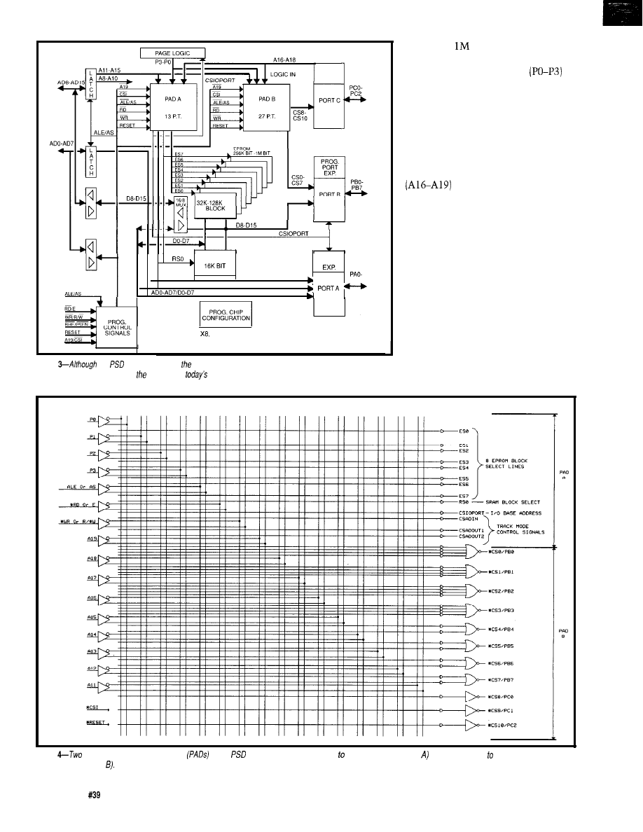
PROG.
PORT
EXP.
PC2
BIT
SRAM
AO-A7
PROG.
PORT
TRACK MODE
SELECTS
PA7
X16
MUX or NON-MUX BUSSES
Figure
the
may appear to
be same as its cousins from the past, the block diagram reveals
much more glue logic to support demands of
small system designs.
bits on the
bit ‘3x3). A built-in
page register controls access to each
block via page select inputs
to
the PAD. A block in which the page
inputs are PAD programmed as “don’t
cares” becomes global and thus a safe
place to put bank switching code and
interrupt vectors.
Besides serving as I/O or chip
selects, port C goes beyond the call of
duty by optionally acting as high-order
address inputs. Al9 can be
further configured to function as an
external
l
CS input, placing the PSD in
low-power standby mode when
inactivated. Finally, the three bits of
port C can even serve as generic PAD
I/O pins, possibly eliminating a little
random logic from your design.
Port A is no slouch either. Besides
I/O, the low-order address inputs of
the PSD can be passed through port A
for connection to other chips. When
used with a nonmultiplexed processor,
port A serves as the data bus.
Figure 5 sums up the myriad
“configuration bits” that define PSD
Figure
programmable address decoders
on the
are used for mapping access internal resources (PAD and generating up eleven chip selects for
external devices (PAD
6 8
Issue
October 1993
The Computer Applications Journal
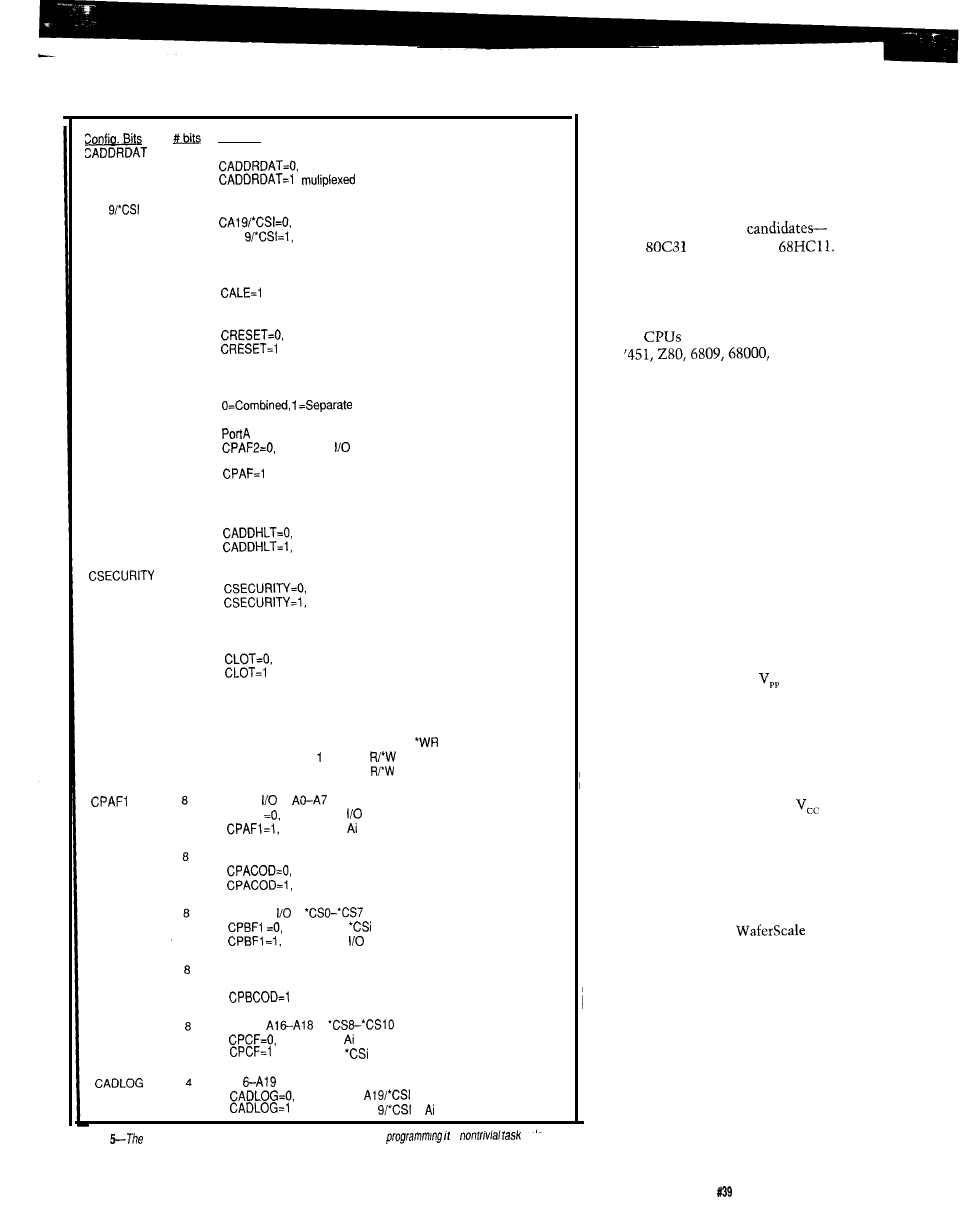
CA1
CALE
CRESET
‘COMBISEP
CPAF2
CADDHLT
CLOT
CRRWR
CEDS
CPACOD
CPBF
CPBCOD
CPCF
2
Function
ADDRESS/DATA Multiplexed (separate buses)
nonmultiplexed
,
Al 9 or
l
CSl
enable power-down
CA1
enable Al 9 input to PAD
Active HIGH or active LOW
CALE=O, Active high
, Active low
Active HIGH or active LOW
Active low reset
, Active high reset
Combined or separate Address Space
for SRAM and EPROM
ADO-AD7 (address/data multiplexed bus)
address or
on Port A
(according to CPAFl)
, address/data multiplexed on Port A
(track mode)
Al 6-A19 Transparent or Latched
Address latch transparent
Address latched (ALE dependent)
SECURITY On/Off
off
on
AO-A15 Address Inputs are transparent or
ALE dependent in nonmultiplexed modes
transparent
, ALE-dependent
Determine the polarity and control methods of
read and write cycles.
CEDS
CRRWR
0
0
‘RD and
active low pulses
0
status and high E pulse
1
1
status and low
l
DS pulse
operation.
There is even a security bit
Port A
or
CPAFl
Port A pin is
Port A pin is (i is between 0 and 7)
Port A is CMOS or Open Drain Output
CMOS output
open drain output
Port El is
is
Port B pin is
(i is between 0 and 7)
Port B pin is
Port B is CMOS or Open Drain Output
CPBCOD=O, CMOS output
, open drain output
Port C
or
Port C pin is (i is between 16 and 18)
, Port C pin is
(i is between 8 and 10)
Al
Address or Logic Input
Port C pin or
is logic input
, Port C pin or Al
is (i is between 16 and 19)
bits in the PSD can make
a
unless you
Figure
vast number of configuration
have tools designed
for the job.
As for any EPROM, burning your
bright ideas into a PSD is a two-step
process. First, you have to create the
hex file, and then you have to program
the chip. However, neither is espe-
cially straightforward for the PSD.
The PSD hex file contains much
more than your program code. You’ve
got to correctly set and locate all fifty
configuration bits as well as the PAD
fuse-map. Putting everything together
by hand is only a job for the very
committed (or those who should be).
When you’re finally ready to blast
the bits into this brainiac,
is raised
to 12.75 V, but that’s where the
similarity to a regular EPROM ends.
The programming algorithm is quite
intricate and involves forcing the chip
into different “modes” in order to
program and verify the PAD’s configu-
ration bits and EPROM. Worse,
must change with the modes across a
five-step range from 4.5 to 6.25 V! All
in all, rolling your own programmer
seems a rather messy proposition.
Some higher end programmers
from third parties can support the
PSD. If yours doesn’t,
offers a nice setup, though admittedly
a little pricey at $1765.00, it’s called a
PSD-Gold. This package includes a
programmer, and PC-based software
called MAPLE. If your programmer
does support the PSD, you can get just
the software by ordering the lower cost
($495) PSD-Silver package.
MAPLE is highly recommended
since it makes the otherwise tedious
task of configuring the PAD and its
many options quick and easy.
The Computer Applications Journal
Issue
October 1993
69
that prevents the configuration and
PAD fuse map from being read.
The vast number of option
permutations allows easy connection
to almost any CPU. Figure 6 shows the
connection of two likely
the Intel
and Motorola
The
Programmable Peripherals Design
and Applications Handbook
from
Waferscale shows the connections and
options settings for many other
popular
including the ‘186, ‘286,
‘196,
and the
68302.
PERILOUS PROGRAMMING

PC0
Figure
can be configured work
either Intel-style
processors such
as the
(a) or Motorola
processors such as
the
PRICE PROVISO
No doubt the PSD is a neat chip,
but success depends on a variety of
factors that ultimately boil down to a
simple question-is it a “good deal?”
The question may be simple, but
the answer isn’t since the optimality
of a particular PSD-based design is
quite application dependent.
For instance, a minimum system
using a
multiplexed bus CPU
(like the ‘186 or ‘196) takes full
advantage of the
on-chip latches
and 16-bit access option. In this case,
the PSD solution is far more stream-
lined than a traditional byte-wide
memory design which would call for
two latches, two
EPROMs, two
bit
and some
glue logic.
On the other hand,
plexed
are not as well served
since the separate data bus consumes
port pins (both port A B in a 16-bit
design, leaving only the 3-bit port C).
Another consideration is sourcing,
the sole nature of which was surely a
factor in the demise of the earlier
combo chips. Besides the well-known
effects of competition on price, supply
reliability shouldn’t be overlooked. As
the old saying goes,
happens.”
A friend of mind recalls the day long
ago when, as a young chip marketer,
he got a call from a frantic
sourced customer that went something
like, “...our overseas guys just called
and said they’re roasting marshmal-
lows at your factory-where are my
parts!” “Fear and loathing” aptly
describes the mood of customers who
get hung out to dry. Fortunately, WSI
recently announced that the PSD is to
be second sourced by Philips, so you
can design it in and still sleep at night.
Yes, priced from $7.92
200 ns) to $11.21 (PSD313, 120 ns) in
the PSD does command a higher
price per bit than commodity memory
chips. However, if you add up the cost
of the equivalent EPROM, SRAM,
latch, glue, and so forth, you’ll see the
PSD isn’t out of line at all. In fact, the
premium is likely offset by PCB cost
and reliability improvements associ-
ated with fewer chips, traces, and pins.
For example, compare a
setup that needs only 112 pins versus
the 200 or so needed for a traditional
design.
The PSD solution is also smaller and
lighter and thus especially well-suited
for portable applications.
All in all, I think the PSD success-
fully walks that fine line between
being “too little too late” and “too
much too soon.” It fills the gap
between the high-end single-chip
and the typical half-dozen or so
commodity chip solution.
Unlike disco and bell bottoms, it’s
time to give “combo chips” like the
PSD another chance. New end graph
WSI isn’t standing still either. Tune in
next month for a look at their brand
new line of bigger and better
q
Tom Cantrell has been an engineer in
Silicon Valley for more than ten years
working on chip, board, and systems
design and marketing. He can be
reached at (510) 657-0264 or by fax at
(510) 657-5441.
Integration, Inc.
47280 Kato Rd.
Fremont, CA 94538
(510) 656-5400
Fax: (510) 657-5916
Philips Semiconductors
8 11 East Arques Ave.
P.O. Box 3409
Sunnyvale, CA 94088-3409
(408) 991-3737
.
416 Very Useful
417 Moderately Useful
418 Not Useful
70
Issue
October 1993
The Computer Applications Journal

Small
Memories
John Dybowski
any embedded
applications
require only small
amounts of read/write
memory. In most cases, the required
memory comes contained within the
microcontroller that you’re using.
Even some fairly elaborate applications
simply don’t require the acquisition
and processing of significant amounts
of data. These applications typically
fall into the domain of small
chip controllers. Sometimes, however,
you need more storage capacity than a
particular controller provides. In this
case you may be forced to add external
memory in the smallest denomination
available to meet your design objec-
tives. Now, although necessary to
completing the task at hand, no one
will argue that such an endeavor
constitutes a singularly uninteresting
topic. And, anyway, how much can
you say about a
RAM chip?
Fortunately that’s not the kind of
memory I plan to talk about here. The
types of small memories will discuss,
unlike the
RAM chip, have
some rather interesting characteristics.
This interest stems not so much from
the memories themselves, but from
the way they can be used, and the way
they are connected to the host control-
ler. It makes sense to use a serial
interface to keep the package size
under control since doing otherwise
would defeat the whole idea. This, of
course, results in a small memory in a
large package. Obviously a pointless
exercise.
In past articles I’ve covered
various two- and three-wire serial
RAM and
devices as well as
serial real-time clocks that also
happened to include varying amounts
of built-in RAM. I will try to avoid
being repetitious and briefly describe
some two- and three-wire RAM chips
that haven’t covered before. Then I’ll
focus on some memory devices that
take interconnection economics to the
limit; devices that carry all their
communications over a single wire.
CLOCKED MEMORIES
Although devices have the
rather desirable attribute of retaining
data with no power whatsoever, there
Photo l-Da//as Semiconductor has two types of touch memory packages available: one
for fixed
(if resembles a transistor package) and other known as a transportable
These stainless
steel holders resemble lithium coin cells.
7 2
Issue
October 1993
The Computer Applications Journal

PARAMETER
SYMBOL MIN TYP MAX. UNITS
Slot
60
Write
Low
0 Low
60
120
Read Data
Read Data Setup
Mode
Equivalent
Mode
T i m e
. . .
Falling Edge
Suspended
Transfer Of One Byte
On The
1 -Wire
Sent
Figure
SIX
definedphases of a one-we transaction include
presence defect, bus command, device command, data
transfer, and CRC. During data transfer, a self-clocking scheme is used.
is a wear-out mechanism that you
must contend with when using these
parts. The limiting factor associated
with
is the write cycle
endurance. This is defined as the
number of times you can write to a
single bit before it stops working.
Although progress has been made in
this regard, and devices with write
cycle endurance in the 100,000 range
are common, some applications will
simply not tolerate this limitation.
It’s easy to determine if an
is an appropriate fit for a
particular application. But you must
keep in mind that a firmware anomaly,
or a system upset, can possibly lead to
unintentionally performing a lot of
write operations that can quickly lead
to the part’s destruction. This is not so
much a problem when using serial
devices, since the access method itself
involves some very specific data
transitions and timing sequences that
narrow the window on such a cata-
strophic event. That’s not to say there
are any guarantees, but the failure
mode would require the code to enter
into a loop that continually, and
explicitly, wrote to the poor memory
device. Because of the protocols in
place in these kinds of systems, this is
an extremely unlikely event.
The situation is more touchy with
parallel devices where the program can
inadvertently enter into a tight “write
loop” without much difficulty and
consume the
in a matter of
seconds. In any event, there
are applications that do
require deliberate, and
frequent, updating of
nonvolatile parameters, and
for these a RAM-based
approach makes the most
sense.
If your design already
supports a three-wire serial
device such as the Dallas
DS 1202 real-time clock, and
you find that its 24 bytes of
nonvolatile RAM is not
sufficient for your needs,
then you may consider
Dallas’s DS 1200 serial RAM
chip. Access to the RAM is
via a three-wire interface
scheme that is electrically
identical to that used in the
DS1202 RTC and is com-
posed of
(reset), C
LK
(clock), and DQ (a bidirec-
tional data) lines. The cost
of adding this part to an
existing design involves
allocating an I/O pin to
function as the RAM’s reset
line since the data and clock
lines can be shared with the
DS1202.
Possessing 1024 bits of
RAM organized as 128
bytes, the DS1200 provides
the mechanisms to access
this RAM either randomly
or sequentially. Random
addressing lets you single
out a particular memory location to
read or write. The sequential address-
ing mode allows you to move data in
and out of the chip in bursts with
address incrementing handled auto-
matically by the internal address
generator at the completion of each
byte transfer. The use of this burst
capability is particularly useful since
the overhead associated with each
access amounts to 24 clocks. These
overhead clocks serve to transfer the
address and command information
prior to any actual operations on the
chip’s internal RAM area.
Available in a
DIP package,
the DS 1200 provides separate power
pins for the main
supply as
well as the battery connection that is
The Computer Applications Journal
Issue
October 1993
7 3
Figure 2-A
standard RS-232
can be configured to
interface with the
Semiconductor one-wire
devices.
required for attaining nonvolatility.
This dual supply connection saves you
the external, low dropout, mixing
diodes and is a feature I’d like to see
more of, especially on chips that have
pins designated as no-connects.
If
is your preference then you
may wish to consider the PCF8570 or
PCF8571
from Signetics. These
parts provide 256 and 128 bytes of
RAM, respectively. Unlike the DS1200
and other 3-wire devices,
imposes
no penalty in the way of requiring
extra pins when new devices are added
to the bus. The chip selection is
handled entirely through the protocol
exchange over the data (SDA) and
clock (SCL) lines. The device address
consists of two portions, where the
four upper bits comprise a fixed base
address with the three low-order bits
providing a user-programmable field
that can be set by jumpering pins on
the IC. Presumably, with this arrange-
ment, you could have up to eight of
these
on the
bus at the same
time, but depending on the system
configuration this may not necessarily
be true.
It turns out that certain other
common device types such as
and
share the same base
address as these RAM chips. This
reduces the amount of RAM devices
that can simultaneously be accommo-
dated. Worse, the larger
use
some of the bits of the programmable
part of the address for paging (due to
the limited scope of the
addressability), which further reduces
the actual number of bus members
that can be accommodated at certain
base addresses. Luckily, this problem
has obviously been encountered and
solved; the
defines a different
base address than the PCF8570,
PCF8571, and the other contending
peripheral chips.
SPARTAN BIT FIELDS
By now, my feeling about all the
proprietary three-wire serial buses on
the market is probably well known. To
summarize: I think the idea of having
a serial standard that requires a chip
select (or reset) line for each added
peripheral is, well...rather restrictive.
In all fairness, there are a lot of
applications where the extra wires
required by such an approach are not a
problem. Nonetheless, for any non-
trivial serial peripheral array, the chip
select lines do tend to add up. It all
boils down to your perspective, your
intentions, and how many I/O pins
you have handy.
Another irritating piece of fallout
associated with the use of a proprietary
interface, especially when using parts
from various manufacturers, is the fact
that often you will need multiple
(mildly tweaked) firmware bit bangers
to cope with the slight bit stream
variations that these parts want to see.
A well-thought-out serial bus like
is clearly superior. If only all the
peripherals we needed were available
with such an interface..
turns out that an apparently
similar amount of effort went into
Listing 1-A
handful of low-level
make writing code to access
one-wire ROM device
easier.
entry points
public
I/O bit
p1.7
data
rseg
rseg
CODE
initialization routine.
if l-wire device is present
push 0
clr
reset pulse
mov
djnz
setb DQ
the line
setb c
mov
driving low?
djnz
0
ret
to read a byte from a l-wire device.
data byte is returned in
Read&Byte:
push 0
mov
bits to read
setb DQ
the line
clr
time-slot
setb DQ
the line
nop
mov
the data bit
(continued)
7 4
Issue
October 1993
The Computer Applications Journal

Listing l-continued
rrc
a
push 0
mov
djnz
0
;pad out time-slot
djnz
until done
setb
:termiate
0
ret
to write a byte to a l-wire device.
byte to write is in
Write-Byte:
push 0
mov
setb DO
nop
nop
rrc
a
mov
8 bits to write
idle the line
start time-slot
emit the data bi
push 0
mov
djnz
0
out time-slot
crafting yet another serial interface.
This interface method, devised by
Dallas, is based on just one signal wire
(and a return lead). This method is
used in their low-cost, one-wire
and ROMs as well in their touch
memory product line. Defining not
only the actual signaling between the
controller and the attached peripher-
als, this methodology also encom-
passes such issues as multidropping
multiple slave devices, sequential
transfers of data, and a clever address
searching scheme for determining
what devices are actually present on
the wire at any given time. you
already like the
concept, then read
on and perhaps you will agree with me
that maybe there’s room for two serial
peripheral standards: a two-wire
standard and a one-wire standard.
Operating a serial interface over a
single wire is not uncommon but there
are surrounding issues associated with
such an approach. Remember that this
single wire must do more than
transport bidirectional data. It must
also allow various higher level
HARDWARE
TRANSCEIVER CHIP
Micromint introduces its
Interface for
is an
chip that automatically handles all the specialized
X-10 timing and bit-shuffling between a computer and a
power line module.
PLIX chip and
sheet
EVALUATION BOARD
100 qty. OEM
PLUS SHIPPING
a lox-cost
into
port.
l-800-635-3355
a
chip and data
all
application
and PC-
Write for a
data sheet
$39.00
Add $30 for
X-IO
PLUS SHIPPING
I N C .
4
PARK ST., VERNON, CT 06066
871-6170 FAX:
$95 EPROM
PROGRAMMER
Super
Fast
P r o g r a m m i n g
to use than others
Does
2764127080
Meg]
The Computer Applications Journal
October1993
75
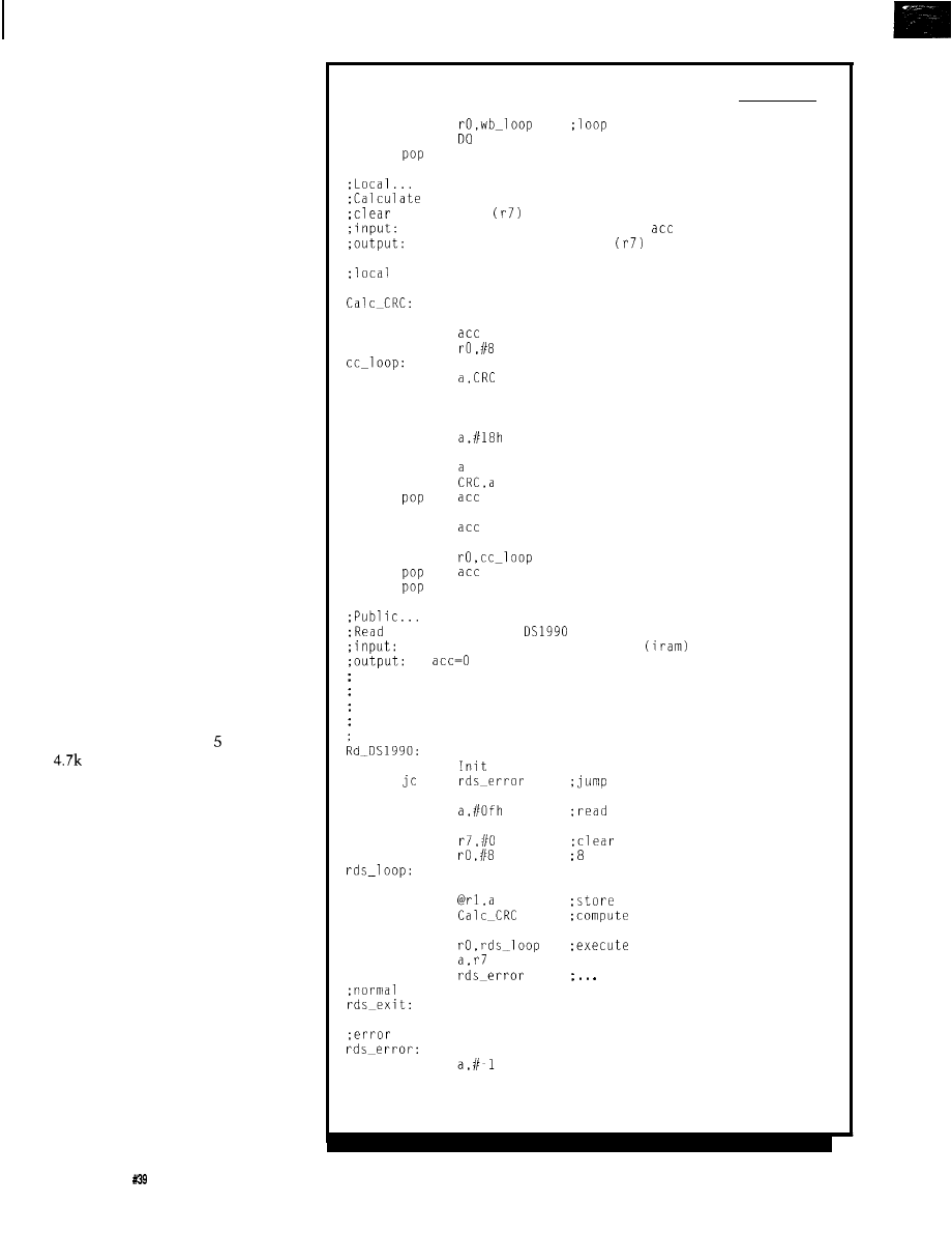
tions such as the passing of command,
status, and address information.
Random or sequential transporting of
data must also be accommodated.
It should be obvious by now that a
very major difference exists between a
serial method that uses a discrete
clock signal, and the self-clocking
mode necessitated when using just one
wire. The main difference is the
discretely clocked scheme is synchro-
nous by nature [and generally can
operate down to DC), but the one-wire
interface employs an asynchronous
technique and mandates that strict,
although well defined, timing param-
eters be adhered to. If the controller
cannot keep up with these restrictions,
device synchronization will be lost and
the transfer sequence will abort. The
situation is eased by the fact that
synchronization is accomplished for
each bit cell and as a result communi-
cations can, in fact, be suspended
between bit transfers.
Dallas describes everything from
detecting when devices connect to the
bus, the actual bit timing for register-
ing ones and zeros, command se-
quences, the definition of the various
transaction sequence phases, and even
a file structure. As with most things,
you can make it as simple or as
complex as you desire. Electrically it’s
another matter; the interface consists
of nothing more than a single wire that
is passively pulled up to volts via a
resistor. Due to the multidropped,
bidirectional nature of the bus, all bus
members (including the master
controller) must use open-drain drivers
to prevent electrical contention
problems. And with the careful
management of line timing, up to
fifteen feet of wire can be driven under
most operating conditions.
Let me proceed by first describing
what to do at the bit level to transfer
ones and zeros between the master
controller and the slave devices.
First of all, data-bit transfers occur
in discrete time intervals called
time
slots
which are started by a falling
edge on the line as driven by the
master controller. This sync pulse
must be held for at least 1 us.
This protocol defines ones or zeros
by short or long low times within a
Listing l-continued
djnz
until done
setb
;termiate time-slot
0
ret
CRC
CRC register
before initial call to this routine.
byte to calculate into CRC is in
new CRC is in CRC register
storage
CRC
set
push
push
mov
xrl
rrc
mov
jnz
xrl
ccl:
rrc
mov
rr
push
djnz
ret
7
0
a
a,CRC
ccl
a
0
a string from the
silicon serial number
rl points to destination buffer
if
then:
the destination buffer contains 8 bytes where:
byte 0 contains the family code
bytes 1 6 contain the serial number
byte 7 contains the CRC
call
mov
call
mov
mov
call
mov
call
inc
djnz
mov
jnz
exi
ret
exit
mov
ret
Write-Byte
Read-Byte
rl
no device
rom command
CRC register
bytes to read
next byte
CRC
read loop
;get computed CRC
should be 0
76
Issue October 1993
The Computer Applications Journal
time slot. A one is registered by
returning the line to a high state
within the sample window. A zero is
written by holding the line low for the
entire duration of the sample window.
Ideally, the master controller
should read the data line 8 from the
beginning of the time slot. When the
slave device transmits data, the master
controller achieves synchronization by
pulling the line low during the
sync time. The slave device controls
the line during the remainder of the
sample window. Communications can
be suspended for any length of time
between time slots by the master
controller leaving the line high. In this
transmission scheme, the data bits are
transmitted LSB first and MSB last.
Now, with the low-level bit
transfer out of the way, I’ll describe
the various second-level transaction
phases in order to help you gain a
better understanding of how the
wire protocol works.
The six defined phases of the
wire transaction sequence are reset,
presence detect, bus command, device
command, data transfer, and cyclical
redundancy check. The six transaction
phases are discussed below.
*Reset-In order to ensure that all
slave devices are listening, the reset
sequence is initiated by the master
controller. The sequence is started
by holding the line low for 480
Following this interval, the master
controller allows the line to return
high for the
presence detect
interval.
*Presence Detect-Following the reset
interval, the slave devices come out
of reset. After 15 from the rising
edge, a slave will drive the line low
for 60 to signal their presence to
the master controller. The duration
of this response allows the master
controller to distinguish this event
from noise on the line.
Command-Once the
master controller has established
the presence of slave devices on the
line, it may issue one of four
level commands as follows:
Through Mode
command allows the master to
access the slave directly without
specifying its
ID number.
This command is only useful when
there is only one slave present on
the line.
ROM Data (33h or
command allows the master to read
the slave’s
family code, 48-bit
serial number, and
CRC. As
with the previous command, this
command can only be used if there
is just a single slave on the line.
-*Match ROM Data
command allows the master to
select a specific slave. The master
sends out a 64-bit number that
includes the family code, the 48-bit
serial number, and a CRC. All bits
must match for this command to be
accepted by the slave.
ROM Data
use of
this command allows the master to
interrogate the slaves in order to
determine the
of all attached
slaves. This command functions as
a repetition of a three-step sequence
our
miniature controllers in
your next product. in
your plant or in your test department. Get 3
range
of analog and digital inputs and outputs. relay and
drivers,
clocks and timers.
our devices
provide serial communications
and
battery-backed
Options
to
keypads. and expansion cards. Our easy-to-use. yet
powerful, Dynamic C
system is only
Prices start at
quantity one.
Sophistication at Low Cost
I D 1 6 0
$ 5 9 5
ID161 (100 MHz) $695
*High Speed
l
8K Trace Buffer
l
16 timing channels
expandable to 32 state channels *Multi-Level Triggering
*State Pass Counting
l
Event Timer/Counter
l
Performance
Histograms *Hardcopy Output *Disassembles S-bit micros
*Supports VGA
l
Demo diskette available
30 Day Money Back Guarantee
INNOTEC DESIGN, INC.
6910 Oslo Circle, Suite 207
Buena Park, CA 90621
Tel: 714-522-1469
38
See us Embedded Systems Booth
The Computer Applications Journal
Issue
October 1993
7 7

that consists of reading a bit,
reading the complement of a bit,
and writing a bit. (Remember that
with their open-drain drivers, the
slave devices can only drive the line
low.) This operation is performed
over the ID bits of each slave until
all of the slave
are known. As
the ID bits are determined in
sequence, the progression is
controlled by the values that are
written as select bits (thereby
incrementally selecting slaves).
Briefly, the result of doing a read of
a true and complemented bit on the
multidrop line can yield the
following values and their associ-
a t e d a s s u m p t i o n s :
are still devices on the
line that have conflicting bits in
this position.
devices on the line have a 0
bit in this position.
devices on the line have a
1
bit in this position.
l-No devices are present.
*Device Command/Data Transac-
tion-Following the transmittal of
the device-specific command, a data
transfer to or from the slave device
takes place. This transfer is carried
out in accordance with the
issued device command.
*CRC-The master controller com-
putes a CRC value over the data as
it is transmitted or received. The
CRC is part of the permanent ID
number that is contained within
ROM devices and is managed by the
master controller for RAM-based
data. In either case, if the
match, the
transfer is assumed
to be error free.
Figure 1 describes how the reset
and the presence-detect phase operates
as well as how the line is managed for
sending and receiving ones and zeros.
The general principle behind how the
internal self-clocking scheme is also
shown pictorially here.
ONE-WIRE PACKAGING
Dallas’s one-wire products are
available in two types of packages:
those intended for fixed PCB mounting
Listing
to communicate with a one-wire device from a high-/eve/language through a
standard serial port.
Transmit 8 bits onto the l-wire data line and receive 8 bits
concurrently. The global variable
must be set to the
port that the COM port adapter is attached to before calling
this routine. This port must also be set to 115200 bps, 8 data, 1
stop, and no parity.
This routine returns the uchar
value
received. it times out waiting for a character then
is
returned.
uchar
outch)
uchar
uint SPA:
uint far *ptr =
far 0x00400000;
ulong far
=
far
ulong M:
get the serial port address
SPA =
Initialize the time limit
M =
+ 2;
wait to TBE and TSRE
do while
0x60) !=
/*flush input
while
get first bit ready to go out
= (outch &
?
: 0x00;
loop to send and receive 8 bits
do
send out the bit
get next bit ready to go out
Mask <<=
= (outch Mask)
: 0x00;
/*shift input char over ready for next bit
inch >>
loop
for
if
to look for the incoming bit
return if out of time
if
return
inch
break
? 0x80 :
while (Mask);
return inch;
return the input char
such as TO92 and SOT223 packages,
lithium coin
stainless cans
and transportable containers such as
(called
touch memories
by Dallas)
the R3 and F5 metal cans. These R3
provide the data signal connection on
and F5 chip carriers are stainless steel
the inner face with the rim used for
holders that physically resemble small
the return.
78
The Computer Applications Journal
RAM- and ROM-based devices are
available in both of these packaging
configurations. The ROM consists of a
factory-lasered 64-bit code that is
made up of an
family code, a
bit serial number, and an
CRC.
These ROM devices are inexpensive
and can be used to provide serializa-
tion and identification information for
various types of electronic instruments
and equipment. Although often
necessary, this type of permanent ID
functionality is frequently hard to
come by economically, especially
when using small and
control-
lers with masked ROMs. The Dallas
ROMs satisfy this need by providing a
unique code in each device-no two
are alike.
Perhaps one possible alternative to
this serialization problem (for moder-
ate-quantity runs) would be to use
OTP PIC processors, where the
programming equipment provides
direct support for sequencing a serial
number with each programming
operation. Using this type of a ROM in
a metal carrier could also provide a
portable alternative to other read-only
auto-identification methods such as
bar codes and magnetic stripes.
One-wire RAM devices are
centered around the same basic ROM
core and provide anywhere from 128 to
bytes of read/write memory. Some
parts provide a single RAM address
space whereas others are partitioned
such that both password secured RAM
areas (for sensitive data), and
secured RAM areas (for use as general
scratch pads) are available. There’s
even a touch device that contains a
built-in real-time clock along with the
ROM and RAM.
BIT BLIPPING
Refer to Listing 1 for code that
demonstrates what is required to pull
off communications with these serial
one-wire devices. So as not to compli-
cate matters, I decided to use the
simplest device in the touch memory
family-the silicon serial number
ROM-for this example. The program
defines functions to initialize the
attached device and determine its
presence, tell it to dump its ID
information, and to read and deposit
this information in an eight-byte
buffer. The CRC is also calculated and
verified to determine if the transfer
completed successfully. Finally, this
success/failure information is con-
veyed back to the calling program.
The main routine first calls the
line initialization function that emits
a reset pulse then looks for a presence
signal on the line. Once a device
responds to the reset sequence, the
read command,
is transmitted via
the write routine. Following the
issuance of the read command, eight
bytes are picked off the line using the
read routine and stored to the data
buffer, with each byte taking part in a
cumulative CRC calculation. If the
CRC checks okay, the routine returns
to the caller with a completion code
indicating success.
As you can see there’s not much
involved in reading from a one-wire
device. You will probably also notice
that some of the routines are some-
what rudimentary and could use
Micromint’s BRUTE-52 is the ultimate compact controller.
One
look at the list of features will tell you that this full-
featured controller has the power to crush your most de-
manding applications:
l
CMOS
.
parallel
. Three
counter timers
l
buffered
high-current outputs
. 11.0592
System Clock
.
DC inputs
l
Hardware Watchdog Timer
.
plus
converter
. Hardware Clock-calendar
60 Samples/second! 1.2
.
Communications
l
digital-to-analog converter
RS-232 or
bps!
2 channels! 1.2
resolution! Selectable
Printer Port,
l
Only 3.5 5.3 Inches!
RS-232 150-9600 bps
. operates at
l
l
Consumes only 100-200
on
l
Up to 56 Kbytes RAM
EPROM
l
Use networked or stand-alone
l
1 Kbit EEPROM
.
ROM
BRUTE-52 offers you all these features at only
100
quantity
OEM)
We also have a starter system for $289. When
you add in Micromint’s renowned quality,
and
support, you won’t
find a better value in compact control.
To order BRUTE-52, or for more information, contact:
Micromint, Inc.
(514) 336
Inquiries
-9426
Invited!
4
Park Street
l
Vernon,
(203) 87
170 .
(203)
CT 06066
872-2204
See us at
Embedded Systems Booth
The Computer Applications Journal
Issue
October 1993
Data Acquisition
and Control
Without Compromise
Programmable Scan Burst
Advanced Industrial Control
boards set a new performance
standard for general purpose
industrial laboratory applications.
ADA2210
A
solution
ADA221 0 features:
n 125
XT throughput
n 16 S.E. 8
analog inputs
n
OV selectable input range
n programmable auto channel scan
n programmable burst mode
n software external triggers, pacer clock
n on-demand DMA transfer
n programmable gain:
n 3 cascadable B-bit counters
n 16 programmable digital I/O lines
n two
analog outputs, selectable range
n
Universal TSR DOS driver
n
Notebook driver
HARDWARE SOLUTIONS
Our AIC family also includes AT
analog
boards,
only A/D control boards for
portable PCs, 4-20
current loopoutputs,
and opto-22 compatibility.
SOFTWARE SOLUTIONS
Select the power and performance of
our library of application programs for moni-
toring, data acquisition and analysis, control,
DSP and 3D graphics.
For
on these and other
ISA
and
products,
call,
or
fax us today!
Place your order now and receive
and
for
Real Time Devices, Inc.
P.O.
Box 906
State
College, PA 16804
(814) 234-8087
n
Fax: (814) 234-5218
further refinement. For example, the
reset/presence detect routine does not
check for a shorted line and only needs
to see the line at a low level for one
sample period before deciding that a
device is connected to the line.
Obviously more could be done to
check for a stuck line and to enhance
glitch rejection. Furthermore, interrupt
masking is not handled at this level.
The issue of interrupts is a real
concern because of the tight timing
constrains imposed by the one-wire
protocol. Obviously the timing would
be wasted by the occurrence of an
interrupt event if it happened at the
wrong time.
In a real implementation, a
number of different approaches could
be taken to resolve this issue and the
particular approach would have to take
into account the operation of the
system as a whole. If interrupts had to
be serviced on an ongoing, although
infrequent, basis, you could mask
interrupts for the duration of the entire
transfer sequence. If the interrupts
occurred more frequently, the best you
could hope for would be to mask the
interrupts for each bit transfer, and
unmask briefly between bits since, at
this time, communications could be
suspended without causing problems.
On the other hand, if the inter-
rupts occurred less frequently but
randomly and had to be serviced in a
timely fashion, there would be no
choice but to let it all hang out and not
mask the interrupts at all, instead
relying on the CRC test to catch
corrupted transactions. In this case,
the transfer would be continually
attempted until successfully com-
pleted or until a retry count expired.
BIG AND LITTLE
Having seen the timing con-
straints involved in communicating
with one-wire devices, you may be
thinking these small memories would
be best serviced using small control-
lers that are good at processing I/O
events in real time. This assumption,
although not unreasonable, is one that
is not true. After having demonstrated
how very small controllers could drive
large memory arrays last month, it
would be a shame not to turn the
tables and connect one of these
minuscule one-wire memories to a real
processor or to an actual computer for
that matter.
It turns out that Dallas supports
the one-wire interface on a PC plat-
form and similar tricks can be used to
link these devices to most processors
using a UART and an RS-232 serial
port. Figure 2 shows how a standard
RS-232 port can be coerced to electri-
cally accommodate standard one-wire
devices using nothing more than a
handful of passive components.
The bit manipulations get a bit
more involved. If the host has a UART
that can operate at up to 115,200 bps,
the time-critical signaling can be
handled almost entirely in hardware
by monkeying with the UART in ways
that it was not intended to be used. Of
course, you realize this amounts to
getting your hands dirty and means
you have to be able to operate down at
the register level. Listing 2 illustrates
how to get the low-level control using
a high-level language. The function
shown is capable of simultaneously
reading and writing eight bits from and
to a one-wire device via an RS-232
port.
If we subscribe to the logic that
less is more, then we can conclude
these one-wire memories amount to a
lot. The fact that these devices come
in small packages and employ a simple
interface can be deceiving since what
may not be immediately apparent is
the amount of engineering that is
actually involved here. This apparent
economy of resources has a balance,
which comes in the form of ideas. If
you want to know more, check out
the volumes of information on this
subject produced by Dallas Semicon-
ductor.
q
Dybowski is an engineer in-
volved in the design and manufacture
of hardware and software for indus-
trial data collection and communica-
tions equipment.
419
Very Useful
420 Moderately Useful
421 Not Useful
80
Issue
October 1993
The Computer Applications Journal
ames, for both children and adults,
represent ideal applications for small,
microprocessors. A micro can
often replace myriad mechanical contraptions
while offering lower cost, smaller size, and improved
performance. This month, I have rounded up nine patent
abstracts on games that employ micros. These range from
classics like the TI Speak-n-Spell to a couple that represent
fundamental technology applicable to many types of games.
I think you will see how microprocessors can not only bring
the latest technology into the home or amusement center,
but can also perform old tasks in better ways.
One of the premier electronic games has been the
Texas Instruments Speak-n-Spell. While voice synthesis on
computers appeared for a long while to be a solution
looking for an application, the TI speech synthesizer
employing advanced LPC encoding brought the familiar,
completely human-like voice into nearly every home.
Abstract 1 is the most recent patent I could find on this
technology. Referenced patent
dated 1985 covers
the same area. All the other references are to devices such
as Federal Screw Works’ landmark synthesizer, speaking
calculators, and so forth.
find to their game cartridge are a pair of design patents
and
dated 1987 and 1988, respectively.
Besides offering market protection for their game, this
mechanism also offers the unique feature of permitting the
user to continue a game at a later time from the same point
where he left off earlier.
The next two abstracts (3 and 4) from SMS Manufactur-
ing represent the same game. The designers here have made
a somewhat “flat” video poker game more interesting by
incorporating the three dimensional action of bouncing
balls. But, as you can see from the wording, the first patent
emphasizes the particulars of their specific poker game
while the other one attempts to generalize the patent to
encompass a wider range of applications. This is a common
technique in patents where one wants to attempt both
specific and general protection. A reading of the abstracts
points up how a single, simple microprocessor coordinates a
variety of user inputs, sensors, and actuators. As is so often
the case, incorporation of a video display provides a dra-
matic, yet low cost, user interface.
The next group of four abstracts (numbers 5 through 8)
represents a varied collection of games which use micropro-
cessors. I have attempted to present a wide range of differ-
ent types of games. In order to conserve on space, I’ve
eliminated all but the pertinent information from the
listings. What is common among all these games is that the
single microprocessor integrates many functions associated
with user control, game dynamics, and feedback of results.
The use of a microprocessor not only simplifies the design,
Abstract 2 presents one of the critical patents for yet
but also permits modes of operation not otherwise feasible.
another household word-Nintendo. This patent-on their
For example, in some games the computer may act as an
memory cartridge-represents the key by which clones of
opponent. It also serves as a source of randomization, score
Nintendo were kept at bay. The earliest references I could
keeping, and often can control multiple games from a single
Patent Number
Issue Date
Inventor(s)
Assignee
US References
US Class
Title
Abstract
1990 11 13
Breedlove, Paul S.; Moore, James H.; Brantingham, George L.; Wiggins, Richard H., Jr.
Texas Instruments Incorporated
3641513.5
Learning aid or game having miniature electronic speech synthesis chip
An electronic hand-held, talking learning aid is disclosed. The learning aid includes a MOS speech
synthesizer chip having an active surface area on the order of 45,000 square mils. The disclosed
speech synthesizer chip includes a digital lattice filter, a voiced/unvoiced excitation circuit, a speech
parameter interpolator, an input parameter decoder, a digital-to-analog converter, and associated timing
circuits. The learning aid is also provided with a microprocessor which functions as a controller for
controlling the operation of the unit. A small speaker is driven by the digital-to-analog converter on the
speech synthesis chip and a keyboard and display device are strobed by the microprocessor controller.
Features include modes in which a speech synthesizer recites instructions or questions to the operator
who must properly respond.
82
Issue
October 1993
The Computer Applications Journal

TALK
Patent Number
Issue Date
Inventor(s)
Assignee
US References
1991 05 14
Satoru; Nishizawa, Kenji
Nintendo Company Limited
4,471 ,163
US Class
2731435 2731856 3641410
Title
Abstract
Memory cartridge and game apparatus using the same
A memory cartridge is
loaded to a game machine which includes a microproces-
sor and a working RAM provided in association with the microprocessor. When the memory cartridge is
loaded to the game machine, a program ROM included in the memory cartridge is connected to the
microprocessor and the working RAM through data bus and address bus such that the data can be
communicated between them. When a game is terminated, a password is generated in accordance with
a program stored in the program ROM in advance by modifying game status data including data of
score, power, or energy, and the stage number which are stored in the working RAM. The password
thus generated is displayed on a display. When the password is inputted by a player prior to consecu-
tively starting a succeeding game in accordance with the display, by restoring the inputted password,
the game status data is set in the working RAM, whereby the microprocessor consecutively starts the
succeeding game from the game status at the timing when the preceding game was terminated.
controller. This is an area where the computing power of
attempts to achieve broad coverage for its concept. It
the microprocessor is not of great concern while cost is. In
represents an interactive playfield-the surface over which
some cases, only simple digital I/O is required, and speed is
the pinball moves and which, in effect, defines the behavior
not paramount. The availability of simple, inexpensive, and
of the game. Their unique use of an image of a human head
low-power controllers like the Microchip PIC series should
for the “preferred” playfield is but one embodiment of their
permit such designs to flourish.
broad patent. I particularly like the moving eyes which
Finally, abstract 9, from Williams Electronic Games
track the course of the ball on the playfield. Keep an eye out
Inc., relates to the ever-popular pinball game. This patent
for this one at your local amusement center.
Patent
Number
Issue Date
Inventor(s)
Assignee
US References
Title
Abstract
1991 05 14
Mirando, Salvatore V.; Lee, Walter
SMS Manufacturing Co., Ltd.
Amusement game
The poker amusement game includes five rubber balls and a playing field with twenty-five openings in
which the rubber balls may reside. A microprocessor has inputs connected to a plurality of switches for
determining the location of the five balls, a plurality of outputs connected to solenoids to be used for
ejecting the balls from the openings, and an output connected to a video display for displaying mes-
sages to the player concerning the play of the game, the points received, etc. When the microprocessor
detects that a coin has been inserted and that the
switch has been pushed, the locations
of the five balls are sensed and the corresponding ejectors are energized to eject the balls in a manner
that causes the balls to randomly bounce in the playing area. Balls coming to rest in the openings cause
switches to close which in turn, will cause the microprocessor to display on the video the identity of the
poker card represented by the occupied openings. The player may discard balls by first activating
appropriate DISCARD switches and then activating the DEAUDRAW switch. In response, the micropro-
cessor energizes the corresponding solenoids to eject the chosen discarded balls from their openings.
The final hand is evaluated when the discarded balls come to rest in their new positions. Tickets or
tokens are awarded based on the value of the final hand.
The Computer Applications Journal
Issue
October 1993

Patent Number
Issue Date
1991 05 14
inventor(s)
Assignee
Mirando, Salvatore V.; Lee, Walter
SMS Manufacturing Corporation
US References
Title
Abstract
Poker roll game
An
device which provides means for the selective release of game pieces, such as balls,
for replay. The amusement/gaming device comprises an array of positions, each position representing a score
in a game such as draw poker. Each position includes a hole to hold a ball in that position and an optical
detector to identify residence of the ball in the hole. An array of rotatable rods having fingers are mounted
below the holes. Solenoids are mounted at the ends of the rods for selectively rotating two intersecting rods to
release the ball allowing return of one or more balls for replay. A microprocessor control and a video display
interact with the player.
Patent Number
Issue Date
1991 04 23
Streeter, Willie L
Title
Abstract
Microcomputer controlled rotation game
A game device for development of coordination and concentration among children as well as adults is
disclosed. The device includes a microprocessor mounted within a housing having indicia representing a pair
of hands and a pair of feet. Each participant has access to four switches operable by the hands and feet. The
microprocessor generates a sequence of tones or lights, each being associated with a hand or foot on the
housing. A pair of arrows may be mounted on the housing to indicate whether the sequence is proceeding
clockwise or counter clockwise. Each participant attempts to repeat the sequence by activating the proper
switch shortly after each tone or light or both. Play continues until a participant makes an error at which point
play ceases. In another embodiment, the game can be played to control the interaction of two participants with
one participant generating a first rotation or random sequence to be repeated by the other participant.
Patent Number
5050,883
Issue Date
1991 09 24
Inventor(s)
Assignee
Goldfarb, Adolph E.; Goldfarb, Martin I.
Goldfarb, Adolph E.
Title
Abstract
Self-contained competitive game for developing spatial sense in young children
Electronics and a playing method stimulate abstract spatial-relations ability, particularly memory of abstract
space, in youngsters-without requiring them to know or spell game commands, or to find keys on a
like keyboard. The game exploits the competitive instinct by rewarding ability to recall complex geometric
abstractions, while yet encouraging play by those who lack that ability. Dedicated manual inputs are used by
each player to enter moves-in the pure form of directions in which the player wishes to go, An audio speaker
signals which player’s move it is, and whether each attempted move is valid. A digital microprocessor is used
to define a maze and each player’s position in it, and to receive moves from the directional inputs, and to
operate the speaker in reply to attempted moves. The processor has no functional connection with any device
for displaying a direct pictorial representation of any part of the maze, and indeed no such direct picture is
electronically developed or shown. The game does include, however, a playing board on which players can in
effect map their own attempts to move through part of the maze-if they are willing to let other players see their
maps.
84
Issue
October 1993
The Computer Applications Journal

Patent abstracts appearing in this column are from the
Automated Patent Searching
database from:
25 Science park
New Haven, CT 06511
(203)
or (800) 648-6787
Russ Reiss holds a Ph.D. in
and has been active in
electronics for over years as industry consultant,
designer, college professor, entrepeneur, and company
president. Using microprocessors since their inception, he
has incorporated them into scores of custom devices and
new products. He may be reached on the Circuit Cellar
BBS or on CompuServe as
422 Very Useful
423 Moderately Useful
424 Not Useful
Patent
Number
5067,079
Issue Date
1991 11 19
Inventor(s)
Assignee
Smith, Jay,
Fort, Jeffrey W.
Smith Engineering
Title
Abstract
Interactive audio baseball game
In a microprocessor based interactive audio game for two users to play against one another, or for one user to
play against the computer, the game having the ability to store and retrieve sets of statistical data correspond-
ing to the performance of actual players, keys for the users to affect the state of the game, and an audio output
for communicating the state of the game or the results of a game play to the users, the audio output for a
particular game state or game play result being variable in order to maintain user interest. A plurality of visual
indicators are arranged in a grid that represents the flight of a thrown ball through a vertical cross section of the
strike zone. Visual indicators are sequentially flashed a predetermined number of times and in a predetermined
pattern for a particular variety of pitch.
Patent Number
5020,806
Issue Date
1991 06 04
Inventor(s)
Assignee
Martin, John
Arachnid, Inc.
Title
Abstract
Multiple target electronic dart game
A multiple target electronic dart game having shared microprocessor that monitors and services operation of
the electronic dart game. The multiple targets are mounted on opposite sides of a column which may be
standing or wall mountable. Affixed to the top of the column is visual display video monitor for providing players
and observers with game scores and the like. The visual display video monitor is optionally capable of
screen presentation. The novel design of the multiple target electronic dart game enables players to play
games not previously available with single target dart games. Moreover, many components utilized by the
controls are shared, thus enabling cost savings by eliminating substantial duplication of components.
Patent Number
Issue Date
1992 09 22
Tastad, Gregory J.
Assignee
William Electronics Games, Inc.
US References
Title
Abstract
Player-operated control system for pinball games
A player-operated control system for pinball games includes a plurality of switch assemblies by which the game
player communicates information regarding the course of play to a controlling microprocessor. The software in
the microprocessor alters the course of play according to the player’s command.
The Computer Applications Journal
Issue
October 1993
85

Davidson
The Circuit Cellar BBS
bps
24 hours/7 days a week
(203)
incoming lines
Vernon, Connecticut
This month, I’ve chosen a pair of message threads that deal with
circuit manufacturing. The first one looks at a problem in manufactur-
ing that is
going to get worse: what kind of solder and flux to use
to avoid having use flux cleaners that harm the environment. The
alternatives are looking promising.
In the second discussion, we take a look at some PC board
design techniques that help shield the circuit from external RF
interference.
Environmentally responsible soldering
From: AL
To: ALL USERS
I just purchased another gallon of Kester 5235 flux
remover to clean some boards. Last time I paid $18.00 a
gallon. This time it cost me $70.00 a gallon. The store says
it’s because of new EPA regs. There goes the price of my
boards.. Unless..
heard a while back of a solder that has
water-soluble flux. You put the boards in a dishwasher to
clean them! Is this true? Who sells this stuff. Is it NASA
approved? Does it hold up to heat and/or moisture? Has
anyone had any experience with this solder?
From: JOHN
To: AL
don’t know if you’re looking for flux-core solder or
bulk flux, but Kester has a few things that might be of
interest to you. There are two RMA “No Clean” solder
pastes, R-244 and
and two water-soluble flux solder
pastes, R-587 and R-588. They have number 245 Low
Residue (no clean) and 33 1 Organic Flux Core solder
soluble flux) in 11 to 3 1 gauge spools.
Their bulk No-Clean fluxes are numbers 95 1, 952, 960,
and
Their water-soluble fluxes are
numbers
1, 233 1
2 120, and 2222.
If you need specs on the ones you’re interested in, leave
a note or you can request Kester’s catalog, phone (708) 297-
1600 (their main office). I’ve had great success with their
No-Clean flux solder,
From: AL
To: JOHN
No Clean? You mean there’s no residue? Where does
the gunk go that allows the solder to flow? I like my boards
86
Issue October 1993
The Computer Applications Journal
to look clean and shiny for my customers. 1’11 get a roll and
try it out.
From: JOHN
To: AL
When the manufacturers say “No Clean,” they really
mean “You Don’t Have To Clean if You Don’t Want To”
The no-clean solder fluxes are really just standard
solders with very low solids content; they still leave a
residue, but it’s *significantly* less than that left by
conventional solders. And there are no long-term problems
with the residue if it’s left on the board. I don’t know of any
cored solders available with water-soluble flux, so the
clean might be your best bet.
From: JIM WHITE To: AL
Both of the boards I currently have in production are
soldered with “no clean” flux solders. One is a through-hole
board which is waved. There is some residue, which is
supposed to be water soluble for water cleaning. The specs
on the flux says it will age well, but the slight tackiness
makes me uneasy. The other board is SMT, and the “no
clean” solder paste actually leaves a clear hard coating over
the solder after IR reflow. This stuff I really like; it is like
getting a little conformal coat (which the high-impedance
sections like) free.
From: AL
To: JIM WHITE
Hmm. I wonder if it would do better or worse in the
humidity of Florida where I have some boards installed.
Would the coating ooz off the board or actually keep the
humidity out. What does the SMT board’s coating do when
you hold it over a pan of boiling water (in steam)?
From: JIM WHITE To: AL
I don’t know. The stuff looks good, but I rely primarily
on the manufacturing people’s research. Both board vendors
are large, high-quality manufacturers who have spent far
more researching this stuff than I ever could. Also, their
reputations and profit are on the line. I did read the product
qualification reports which claim that these no-wash fluxes

retain the correct properties for a long time, including
temperature and humidity changes.
One guy I know has his business in
He has
an adapter board which is assembled there. They used some
no-wash flux (through-hole board) which grew some kind of
fuzzy-looking crystal in the humidity. The flux in the
solder went into solution then
in the high
humidity and temperature. The boards worked fine, the
crystals were not conductive, but the boards were aestheti-
cally unacceptable.
From: JOHN
To: AL
I don’t know brand, but we use such a solder on our
wave line. We used to have a dishwasher to clean up the
boards! Now have a larger and more dignified washer.
We also have used water-soluble flux solder for hand
solder. In my experience, it is harder to get a good joint, as
it doesn’t seem to clean as well as rosin. it also eats solder-
ing iron tips, and smells horrid. The production line has no
problems, however.
PC board design for
rejection
From: JOHN
To: ALL USERS
I’m in the process of laying out a small PC board for use
in a severe
environment. I’m new to PCB design and am
using this board to teach myself the things I need to know
to go on to more complex layouts.
The board only needs one side for traces and I was
wondering if it was better to place a ground plane on the
component side (by itself) or the solder side of the board,
surrounding the traces. If on the component side, it would
be connected to the ground net at each plated-through
ground pin (there are
11
of them).
The device will be operated in an arena with dozens of
UHF and VHF walkie talkies and a few repeaters.
Will either of these layouts provide a bit more resistance to
RFI, or just more resistance to interference by its own
components? I’ve read Coomb’s “Printed Circuits Hand-
book” and Ginsberg’s “Printed Circuits Design” and
couldn’t find an answer, though I learned a *lot* of other
things I needed to know.
From: PAUL PETERSEN To: JOHN
To some extent it depends on what kind of circuit
you’re designing. If it’s RF up in the megahertz region, then
you’ll want to consider impedance of copper runs, and so
forth. Having a ground plane on the solder side adds
capacitance. Actually, if you’re worried about picking up
stray RF interference, your best bet is to put everything in
an RF-tight box using copper screen at the seals and
overlapping metal joints. Metal-to-metal with sheet metal
screws will only leak RF. Not knowing what your design is,
I’d say try it the cheap way and if it works you’re home, if
not, you have an option to fall back on.
From: JOHN
To: PAUL PETERSEN
My circuit is a small interface being used as a universal
front end for several different electronic flash units we use.
The interface lets us parallel several units together to
simplify cabling. It’s probably going to be in a plastic case
because of the extraordinary abuse it gets; the small Serpac
cases just bounce, no dents. I’ve only had one occasion
where
has interfered with the operation of a couple of
my hand-wired prototypes, but since its so easy to add
ground planes and to backfill with copper, I thought I might
as well do as much as I can to prevent that from happening
again.
From: JOHN
To: PAUL PETERSEN
Oops, I forgot to mention that it’s strictly a
frequency board; CMOS 555,
and some caps and resistors, 9-volt battery powered. The
unit sits on standby, drawing about 1
and powers up in a
couple of microseconds when the input is shorted by the
camera’s shutter contacts (PC connection). It then fires the
flash unit and powers back down. All in
10
milliseconds.
The board will fire the flash for
rolls of film a day for
years before you have to replace the battery (on paper that
is, I’m changing batteries each year
From: JAMES MEYER To: JOHN
My experiences lead me to believe that board layout
will not make very much difference in reducing the sensi-
tivity of a circuit to externally generated RF. A closed metal
box is 99% of the solution. You also have to be very careful
with each and every wire that passes into the box. The best
shielding is ruined if you connect an antenna to the circuit
through a hole in the shielding. Any wire connected to your
circuit from the outside must be considered to be an
antenna and treated to remove the RF from it.
From: JOHN
To: JAMES MEYER
Thanks for the feedback, I’m looking into putting the
circuit into a small metal box before assembling everything
The Computer Applications Journal
October 1993
87
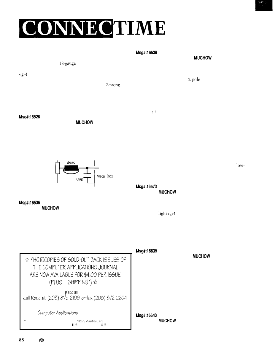
into a larger plastic box (needed for aesthetic and abuse
reasons). My biggest problem is the run of cable up to the
unit which is usually
zip cord, up to 1000 feet in
length. How’s *that
l
for an unwanted antenna problem
We can’t switch cable type since that’s what every
sport photographer uses to hook up his equipment and we
have to be compatible with it, including using
female household receptacles as the input and output
connectors! Amazingly, no one has been injured by plugging
the wrong cord into the wall instead of a camera or flash
pack.
From: JAMES MEYER To: JOHN
Ferrite beads and a small ceramic disc cap on each wire
that comes out of the metal box should help. If the metal
box were enough smaller than the plastic box, then you
could put the connector on the plastic box, and add the
filter just before the (short) wire went into the metal box as
follows:
Connector
Plastic Box
From: JOHN
To: JAMES MEYER
In fact, there is a bit of room between the plastic case
and the metal one I was considering. The connectors will
have to go on the plastic case for aesthetic reasons, so your
idea sounds like the best compromise. Does the wire have
to pass through the bead more than once (is the attenuation
greater if I do loop it?) because I’ll need a large bead then,
and I don’t have
l
that* much room.
From: JAMES MEYER To: JOHN
to
order,
Here's yourchancetocompleteyour
Journal library!
The wire *can* go more than once through the bead if
it’s big enough, but it doesn’t *have* to. Within limits, the
more turns you make through the bead, the more filtering.
If you need more filtering, you could also just put *two*
beads on the wire. Also be careful if you use bare wires.
Some beads are conductive. I found out the hard way.
One good source of large and small beads is to tear up
old switching type computer power supplies. You can find
lots of good parts in dead supplies.
All orders must be prepaid. Check,
or International
From: JOHN
To: JAMES MEYER
Postal Money Order accepted.
funds drawn on
bank only.
I’ll get a few beads and play with the scope to see how
From: TODD NICHOLS To: JOHN
When you run that wire through a ferrite bead, you are
making a toroidal inductor. Looping the wire increases the
inductance (more turns around the “core”). That whole
series-L/shunt-C circuit is a
low-pass filter, and
when you increase the series inductance, you’re just
lowering the cutoff frequency. You can even select the
inductance and capacitance for a given level of attenuation
at some frequency. If you have some idea of the kinds of
hash you have to deal with in the vicinity of your long-wire
antenna then you can design your input filters for a
certain immunity level. Also, I echo a previous comment
about a shield only being effective if you don’t let EM1 in
through some hole somewhere.
Have you considered using feedthrough capacitors?
They are shaped like a small bolt (6-32 or so in size); drill a
hole in your metal box, pop one in, tighten the nut, and you
have a wire running through the box. The neat thing is the
wire runs through a dielectric material, and there is capaci-
tance from that wire to ground-just like the shunt capaci-
tance in the proposed input filter. That’s a single-pole
pass filter. The microwave and RF industry use these a lot.
They don’t take up much room.
From: JOHN
To: TODD NICHOLS
I heard of feedthrough caps, but have never used them.
I like the idea.
The hash on my input line is pretty well spread out
from DC to
I know I can’t block it all, or even
most of it, but it would be nice to block as much as I can
without spending a fortune protecting these devices. They
only cost me $30 or so and an afternoon to build. I don’t
want to spend $100 protecting them from RFI! They just
don’t misbehave enough to justify the expense.
Issue
October 1993
The Computer Applications Journal

much of a difference more turns make, and how it compares
to adding another bead. The computer power supply tip was
very timely. A friend of mine just had his systems supply
die two days ago and he hasn’t thrown it away. It’s mine
tomorrow! Thanks!
From: PELLERVO
To: JOHN
A tall challenge for any filtering you are talking! You
say that the hash pretty much covers the spectrum of DC to
light. Yet you would want to have your detector see an edge
to provide the synchronization. That means you cannot
slow down too much with the filtering!
Actually, as much as I like the feedthrough capacitors
and ferrite beads in noisy environment, I have a word or
two of caution about selecting and using them. I also may
have a “real” solution. Let’s see.
The feedthrough devices come in two classes, one is
just what the name says, with capacitances up to several
nanofarads. That in principle adds to whatever capacitance
(probably tens of picofarads per foot) your cable has. The
other class has less capacitance but also includes a ferrite
bead structure. Sort of a distributed series inductance/
parallel capacitance. In other terms, such a thing is called a
delay line. However, a delay line is not supposed to attenu-
ate anything, so the ferrite is normally made quite
In other terms, it has a resistive element in the form of an
eddy current path. But all of that still is quite high in the
frequency band, several megahertz. Now, to the nature of
your wiring and the noise signal..
If I understand, you have just plain unshielded, un-
twisted pair. And you have several of the receivers in
parallel along this long transmission line. Yes, transmission
line, and not so simple: you also have the third conductor in
shape of the ground or the concrete structure or whatever
the wires and boxes are laying upon. Thereby you have a
ground-referenced antenna of sorts. Two things about this
to keep in mind: Your signal should be differential while
the noise induced into the two wires should be equal and
canceling
each other in your differential sense. And second,
you have the impedance mismatches to count at every
point where you put a receiver. Now, you might start seeing
where I am coming to.
The feedthrough capacitors should be minimal in
capacitance value, because they again represent an imped-
ance mismatch in addition to potentially slowing your
desired signal
too much.
The ferrite beads should be used as a common-mode
filtering device, that is, both the lines entering the receiver
boxes would go through the same opening in the toroid as a
pair. This arrangement filters the common-mode noise, but
leaves the signal pretty much untouched. It also leaves any
noise that already has gotten into your differential domain
untouched.
Toward the more proven techniques, you should try to
match the line impedance as best you can. That means a
terminating resistance of about 100 to 150 ohms at the very
far end of the line and attenuating structures at the boxes
along the line just like the cable TV systems have. Say
something like 600 ohms in, rather than the same 100 to
150 ohms at each place. I think there would be no need to
avoid impedance mismatches within each receiver.
Now, all this means that in essence you have to
provide a great jolt into the cable as your signal. Say, you
put in a pulse of 20 V and your impedance is the lower end
of the above-mentioned range, 100 ohms. Then you have to
provide a
pulse. If that does not mask the noise
from the antenna, then hardly anything does!
To emphasize, try to keep the receivers as symmetrical
as possible relative to earth (your third conductor] because
the unsymmetry more than anything is a cause of hash
pickup. Therefore, don’t think one of the two wires in the
cable is the “neutral side” and the other one the hot side.
Build everything symmetrical and minimize capacitances
and capacitance differences to the inner shielded box. Use
optocouplers or whatever suitable devices for maximum
benefit in this particular sense. I am somewhat skeptical
about your ability to change the governing principles at this
time in the project, but at least I have tried to enlighten the
universe, haven’t I?
We invite you call the Circuit Cellar BBS and exchange
messages and files with other Circuit Cellar readers. It is
available 24 hours a day and may be reached at (203)
1988. Set your modem for 8 data bits, stop bit, no parity,
and 300,
9600, or
bps.
Software for the articles in this and past issues of The
Computer Applications
may be downloaded from
the Circuit Cellar BBS free of charge. For those unable to
download files, the software is also available on one 360K
IBM PC-format disk for only $12.
To order Software on Disk, send check or money order
to: The Computer Applications Journal, Software On Disk,
P.O. Box 772, Vernon, CT 06066, or use your VISA or
Mastercard and call (203) 875-2199. Be sure to specify the
issue number of each disk you order. Please add $3 for
shipping outside the U.S.
425 Very Useful
426 Moderately Useful
427 Not Useful
The Computer Applications Journal
October 1993
8 9
The Race for Power
seems that about every 18 months we get a new processor. In my experience, most PC buyers can’t
justify buying a new computer every time a new generation comes along. Of course, there will always be
technophiles who must own the latest platform, but the majority of us have hardly touched the performance envelope
of the present generation before we are beseeched to join the latest development frenzy and instant obsolescence mentality.
New generations of processors appear so fast that the previous generation becomes “market obsolete” even before most
software vendors have figured out how to write code for maximum utilization. In their race for market share, software companies can’t
afford to take the time to optimize existing code using enhanced instructions every time a new processor comes along. They just
have to reformulate what they have to be “code compatible” and shove it out the door. Is this why “entry level” systems require
drives?
Even the compiler folks struggle to stay ahead of the eight ball. So what do we get? A bunch of ‘486s running 8086 code? 25
MIPS of
What good is a cache if the programs aren’t cache aware and completely flush the cache every few instructions? Sure
my old programs run faster, but I would much rather have a program that really used the processor, not just the increased clock speed.
Unfortunately, by the time software tools get debugged and price competitive for a particular generation, that processor is being
obsoleted by the marketeers at
Inc. who are telling the developers that it is time to move on. This frenetic pace is
exacerbated more when a new processor is just “simply” dropped into an existing architecture (just add a little bit of patching logic).
Little thought is given to designing a new system architecture that genuinely capitalizes on the horsepower of the new chip for any
particular application.
To offset bandwidth inadequacy of an old bus architecture, designers compensate by unloading low-level processor functions
through extensive use of video, sound, math, mass storage, communications, and you-name-it
While the idea of
distributed processing is a good one, how sensible is it if each of these processors (and the main system processor) is only running at
a fraction of its capacity? And in an architecture not akin to even supporting coprocessing to begin with? Now I ask you, does this
make sense?
What happens to all of these “obsolete” chips? Look at the number of embeddable ‘386s and ‘486s. Unless these things are
steering satellites and rockets, it seems a bit of an overkill. It’s like using a sledgehammer to drive tacks. The more generations
between those “obsolete” processors and the and
“stone-age” microcontrollers that most of us would actually choose in an
embedded control application, the more we feel the need to justify this choice. Do you really need
to run a few dozen
motors and lights?
I guess my conclusion is that bigger, badder, more potent chips is not a panacea nor does it necessarily improve application
software. What we as engineers need to do is slow down long enough to think about better ways to apply what we already have
available to us. If that doesn’t work, then maybe Tom Cantrell is right. Just give me a processor with about 50 instructions and then you
can do whatever you want each generation to make those 50 instructions go faster.
96
Issue October
1993
The Computer Applications Journal
Wyszukiwarka
Podobne podstrony:
circuit cellar1990 10,11
circuit cellar2002 10
circuit cellar1996 10
circuit cellar1995 10
circuit cellar2004 10
circuit cellar1991 10,11
circuit cellar1992 10,11
circuit cellar1994 10
circuit cellar2003 10
circuit cellar1993 10
circuit cellar1997 10
circuit cellar2001 10
circuit cellar2000 10
circuit cellar1990 10,11
circuit cellar1991 10,11
circuit cellar2003 10
circuit cellar1994 10
circuit cellar1997 10
więcej podobnych podstron