
April 2010
Doc ID 15491 Rev 3
1/154
PM0056
Programming manual
STM32F10xxx Cortex-M3 programming manual
This programming manual provides information for application and system-level software
developers. It gives a full description of the STM32F10xxx Cortex™-M3 processor
programming model, instruction set and core peripherals.
The STM32F10xxx Cortex
™
-M3 processor is a high performance 32-bit processor designed
for the microcontroller market. It offers significant benefits to developers, including:
●
Outstanding processing performance combined with fast interrupt handling
●
Enhanced system debug with extensive breakpoint and trace capabilities
●
Efficient processor core, system and memories
●
Ultra-low power consumption with integrated sleep modes
●
Platform security

Contents
PM0056
Doc ID 15491 Rev 3
Contents
About this document . . . . . . . . . . . . . . . . . . . . . . . . . . . . . . . . . . . . . . . 10
Typographical conventions . . . . . . . . . . . . . . . . . . . . . . . . . . . . . . . . . . . . 10
List of abbreviations for registers . . . . . . . . . . . . . . . . . . . . . . . . . . . . . . . 10
About the STM32 Cortex-M3 processor and core peripherals . . . . . . . . . 10
Integrated configurable debug . . . . . . . . . . . . . . . . . . . . . . . . . . . . . . . . 11
Cortex-M3 processor features and benefits summary . . . . . . . . . . . . . . 12
Cortex-M3 core peripherals . . . . . . . . . . . . . . . . . . . . . . . . . . . . . . . . . . 13
The Cortex-M3 processor . . . . . . . . . . . . . . . . . . . . . . . . . . . . . . . . . . . . 14
Processor mode and privilege levels for software execution . . . . . . . . . 14
Exceptions and interrupts . . . . . . . . . . . . . . . . . . . . . . . . . . . . . . . . . . . 23
The Cortex microcontroller software interface standard (CMSIS) . . . . . 24
Memory regions, types and attributes . . . . . . . . . . . . . . . . . . . . . . . . . . 26
Memory system ordering of memory accesses . . . . . . . . . . . . . . . . . . . 27
Behavior of memory accesses . . . . . . . . . . . . . . . . . . . . . . . . . . . . . . . . 27
Software ordering of memory accesses . . . . . . . . . . . . . . . . . . . . . . . . 28
Memory endianness . . . . . . . . . . . . . . . . . . . . . . . . . . . . . . . . . . . . . . . 31
Synchronization primitives . . . . . . . . . . . . . . . . . . . . . . . . . . . . . . . . . . . 32
Programming hints for the synchronization primitives . . . . . . . . . . . . . . 33
Exception entry and return . . . . . . . . . . . . . . . . . . . . . . . . . . . . . . . . . . 38

PM0056
Contents
Doc ID 15491 Rev 3
3/154
Fault escalation and hard faults . . . . . . . . . . . . . . . . . . . . . . . . . . . . . . . 42
Fault status registers and fault address registers . . . . . . . . . . . . . . . . . 43
Entering sleep mode . . . . . . . . . . . . . . . . . . . . . . . . . . . . . . . . . . . . . . . 44
Wakeup from sleep mode . . . . . . . . . . . . . . . . . . . . . . . . . . . . . . . . . . . 44
The external event input . . . . . . . . . . . . . . . . . . . . . . . . . . . . . . . . . . . . 45
Power management programming hints . . . . . . . . . . . . . . . . . . . . . . . . 45
The Cortex-M3 instruction set . . . . . . . . . . . . . . . . . . . . . . . . . . . . . . . . 46
About the instruction descriptions . . . . . . . . . . . . . . . . . . . . . . . . . . . . . . 52
Restrictions when using PC or SP . . . . . . . . . . . . . . . . . . . . . . . . . . . . . 53
Flexible second operand . . . . . . . . . . . . . . . . . . . . . . . . . . . . . . . . . . . . 53
PC-relative expressions . . . . . . . . . . . . . . . . . . . . . . . . . . . . . . . . . . . . . 57
Instruction width selection . . . . . . . . . . . . . . . . . . . . . . . . . . . . . . . . . . . 60
Memory access instructions . . . . . . . . . . . . . . . . . . . . . . . . . . . . . . . . . . . 61
LDR and STR, immediate offset . . . . . . . . . . . . . . . . . . . . . . . . . . . . . . 62
LDR and STR, register offset . . . . . . . . . . . . . . . . . . . . . . . . . . . . . . . . . 64
LDR and STR, unprivileged . . . . . . . . . . . . . . . . . . . . . . . . . . . . . . . . . . 65
LDREX and STREX . . . . . . . . . . . . . . . . . . . . . . . . . . . . . . . . . . . . . . . . 71
General data processing instructions . . . . . . . . . . . . . . . . . . . . . . . . . . . . 73
ADD, ADC, SUB, SBC, and RSB . . . . . . . . . . . . . . . . . . . . . . . . . . . . . . 74
AND, ORR, EOR, BIC, and ORN . . . . . . . . . . . . . . . . . . . . . . . . . . . . . . 76

Contents
PM0056
Doc ID 15491 Rev 3
ASR, LSL, LSR, ROR, and RRX . . . . . . . . . . . . . . . . . . . . . . . . . . . . . . 77
REV, REV16, REVSH, and RBIT . . . . . . . . . . . . . . . . . . . . . . . . . . . . . . 82
Multiply and divide instructions . . . . . . . . . . . . . . . . . . . . . . . . . . . . . . . . 84
MUL, MLA, and MLS . . . . . . . . . . . . . . . . . . . . . . . . . . . . . . . . . . . . . . . 84
UMULL, UMLAL, SMULL, and SMLAL . . . . . . . . . . . . . . . . . . . . . . . . . 86
SBFX and UBFX . . . . . . . . . . . . . . . . . . . . . . . . . . . . . . . . . . . . . . . . . . 90
Branch and control instructions . . . . . . . . . . . . . . . . . . . . . . . . . . . . . . . 92

PM0056
Contents
Doc ID 15491 Rev 3
5/154
About the STM32 core peripherals . . . . . . . . . . . . . . . . . . . . . . . . . . . . 106
Memory protection unit (MPU) . . . . . . . . . . . . . . . . . . . . . . . . . . . . . . . . 106
MPU access permission attributes . . . . . . . . . . . . . . . . . . . . . . . . . . . 107
MPU mismatch . . . . . . . . . . . . . . . . . . . . . . . . . . . . . . . . . . . . . . . . . . 109
Updating an MPU region . . . . . . . . . . . . . . . . . . . . . . . . . . . . . . . . . . . 109
MPU design hints and tips . . . . . . . . . . . . . . . . . . . . . . . . . . . . . . . . . . 111
MPU type register (MPU_TYPER) . . . . . . . . . . . . . . . . . . . . . . . . . . . . 112
MPU control register (MPU_CR) . . . . . . . . . . . . . . . . . . . . . . . . . . . . . 113
MPU region number register (MPU_RNR) . . . . . . . . . . . . . . . . . . . . . 114
MPU region base address register (MPU_RBAR) . . . . . . . . . . . . . . . . 115
MPU region attribute and size register (MPU_RASR) . . . . . . . . . . . . . 117
Nested vectored interrupt controller (NVIC) . . . . . . . . . . . . . . . . . . . . . . 119
The CMSIS mapping of the Cortex-M3 NVIC registers . . . . . . . . . . . . 120
Interrupt set-enable registers (NVIC_ISERx) . . . . . . . . . . . . . . . . . . . . 121
Interrupt clear-enable registers (NVIC_ICERx) . . . . . . . . . . . . . . . . . . 122
Interrupt set-pending registers (NVIC_ISPRx) . . . . . . . . . . . . . . . . . . . 123
Interrupt clear-pending registers (NVIC_ICPRx) . . . . . . . . . . . . . . . . . 124
Interrupt active bit registers (NVIC_IABRx) . . . . . . . . . . . . . . . . . . . . . 125
Interrupt priority registers (NVIC_IPRx) . . . . . . . . . . . . . . . . . . . . . . . . 126
Software trigger interrupt register (NVIC_STIR) . . . . . . . . . . . . . . . . . 127
Level-sensitive and pulse interrupts . . . . . . . . . . . . . . . . . . . . . . . . . . . 127
NVIC design hints and tips . . . . . . . . . . . . . . . . . . . . . . . . . . . . . . . . . 128
System control block (SCB) . . . . . . . . . . . . . . . . . . . . . . . . . . . . . . . . . . 130
CPUID base register (SCB_CPUID) . . . . . . . . . . . . . . . . . . . . . . . . . . 130
Interrupt control and state register (SCB_ICSR) . . . . . . . . . . . . . . . . . 131
Vector table offset register (SCB_VTOR) . . . . . . . . . . . . . . . . . . . . . . . 133
Application interrupt and reset control register (SCB_AIRCR) . . . . . . 134
System control register (SCB_SCR) . . . . . . . . . . . . . . . . . . . . . . . . . . 135
Configuration and control register (SCB_CCR) . . . . . . . . . . . . . . . . . . 136
System handler priority registers (SHPRx) . . . . . . . . . . . . . . . . . . . . . 137
System handler control and state register (SCB_SHCSR) . . . . . . . . . 139
Configurable fault status register (SCB_CFSR) . . . . . . . . . . . . . . . . . . 141
Hard fault status register (SCB_HFSR) . . . . . . . . . . . . . . . . . . . . . . . . 144
Memory management fault address register (SCB_MMFAR) . . . . . . . 146
Bus fault address register (SCB_BFAR) . . . . . . . . . . . . . . . . . . . . . . . 146
System control block design hints and tips . . . . . . . . . . . . . . . . . . . . . 147

Contents
PM0056
Doc ID 15491 Rev 3
SCB register map . . . . . . . . . . . . . . . . . . . . . . . . . . . . . . . . . . . . . . . . 147
SysTick control and status register (STK_CTRL) . . . . . . . . . . . . . . . . 148
SysTick reload value register (STK_LOAD) . . . . . . . . . . . . . . . . . . . . . 149
SysTick current value register (STK_VAL) . . . . . . . . . . . . . . . . . . . . . . 151
SysTick calibration value register (STK_CALIB) . . . . . . . . . . . . . . . . . 151
SysTick design hints and tips . . . . . . . . . . . . . . . . . . . . . . . . . . . . . . . . 152
SysTick register map . . . . . . . . . . . . . . . . . . . . . . . . . . . . . . . . . . . . . . 152

PM0056
List of tables
Doc ID 15491 Rev 3
7/154
List of tables
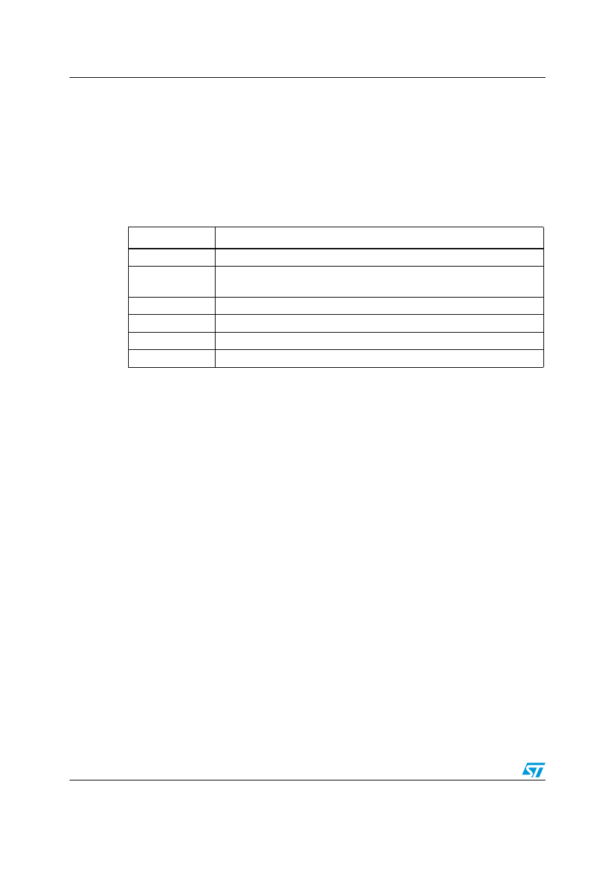
Summary of processor mode, execution privilege level, and stack use options. . . . . . . . . 15
label-PC offset ranges . . . . . . . . . . . . . . . . . . . . . . . . . . . . . . . . . . . . . . . . . . . . . . . . . . . . 67

List of tables
PM0056
Doc ID 15491 Rev 3


About this document
PM0056
Doc ID 15491 Rev 3
1 About
this
document
This document provides the information required for application and system-level software
development. It does not provide information on debug components, features, or operation.
This material is for microcontroller software and hardware engineers, including those who
have no experience of ARM products.
1.1 Typographical
conventions
The typographical conventions used in this document are:
1.2
List of abbreviations for registers
The following abbreviations are used in register descriptions:
1.3
About the STM32 Cortex-M3 processor and core peripherals
The Cortex-M3 processor is built on a high-performance processor core, with a 3-stage
pipeline Harvard architecture, making it ideal for demanding embedded applications. The
processor delivers exceptional power efficiency through an efficient instruction set and
extensively optimized design, providing high-end processing hardware including single-
cycle 32x32 multiplication and dedicated hardware division.
italic
Highlights important notes, introduces special terminology, denotes
internal cross-references, and citations.
< and >
Enclose replaceable terms for assembler syntax where they appear
in code or code fragments. For example:
LDRSB<cond> <Rt>, [<Rn>, #<offset>]
read/write (rw)
Software can read and write to these bits.
read-only (r)
Software can only read these bits.
write-only (w)
Software can only write to this bit. Reading the bit returns the reset
value.
read/clear (rc_w1) Software can read as well as clear this bit by writing 1. Writing ‘0’ has
no effect on the bit value.
read/clear (rc_w0) Software can read as well as clear this bit by writing 0. Writing ‘1’ has
no effect on the bit value.
toggle (t)
Software can only toggle this bit by writing ‘1’. Writing ‘0’ has no effect.
Reserved (Res.)
Reserved bit, must be kept at reset value.
PM0056
About this document
Doc ID 15491 Rev 3
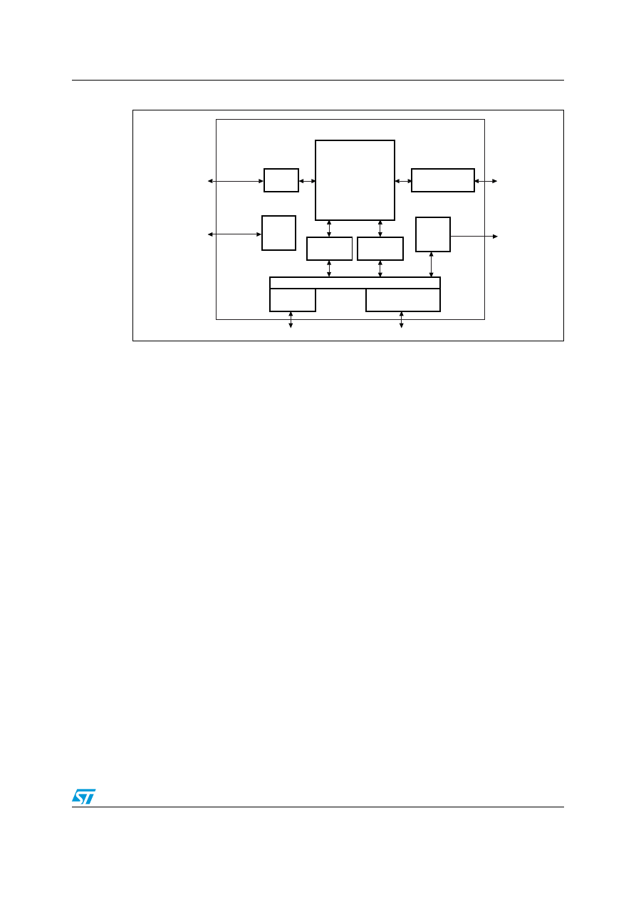
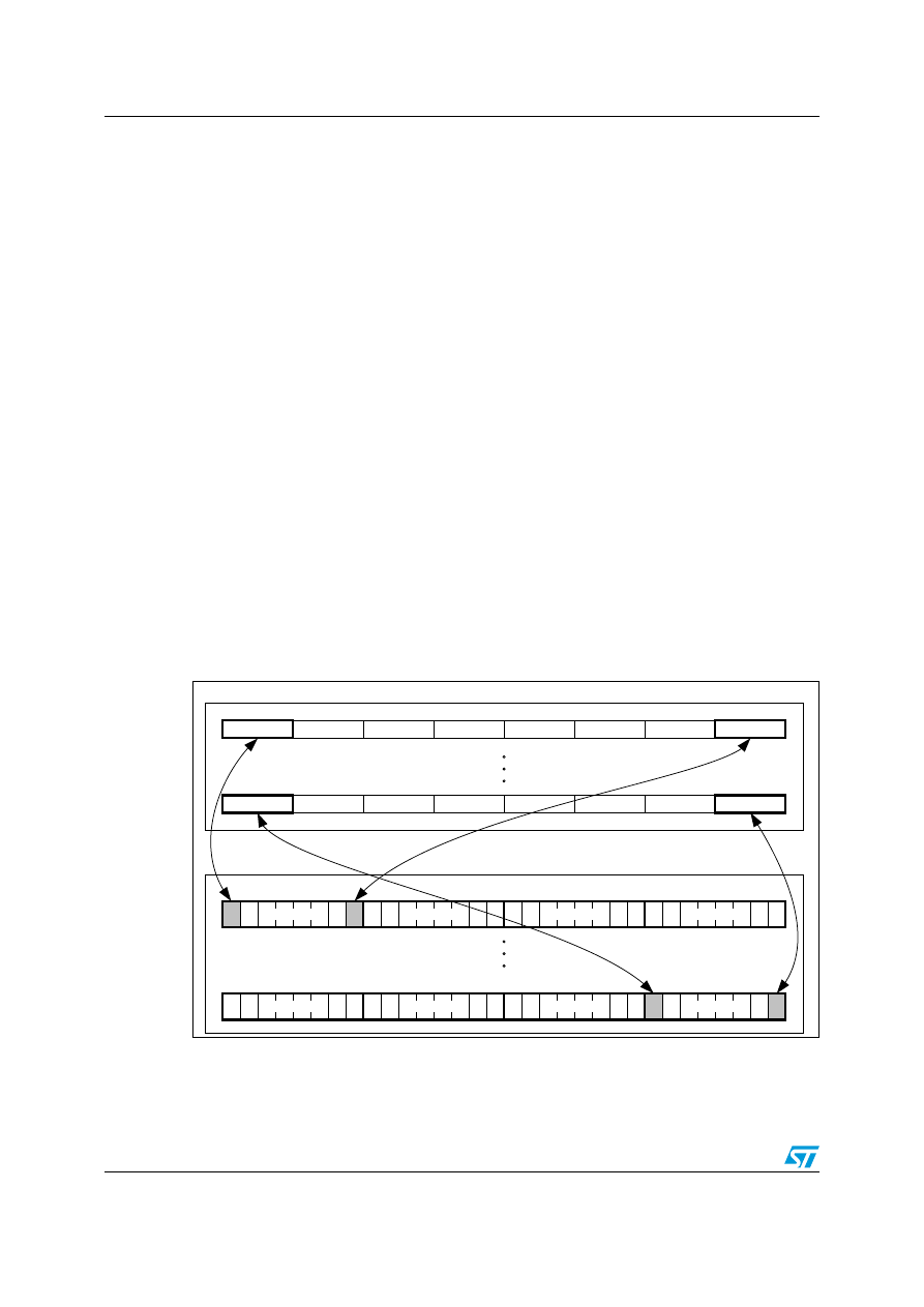
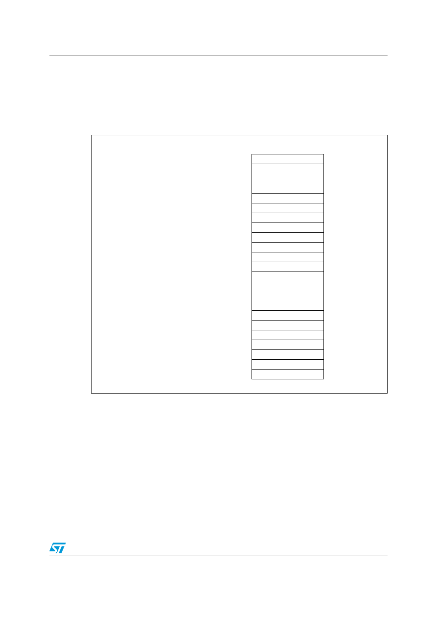
Figure 1.
STM32 Cortex-M3 implementation
To facilitate the design of cost-sensitive devices, the Cortex-M3 processor implements
tightly-coupled system components that reduce processor area while significantly improving
interrupt handling and system debug capabilities. The Cortex-M3 processor implements a
version of the Thumb
®
instruction set, ensuring high code density and reduced program
memory requirements. The Cortex-M3 instruction set provides the exceptional performance
expected of a modern 32-bit architecture, with the high code density of 8-bit and 16-bit
microcontrollers.
The Cortex-M3 processor closely integrates a configurable nested interrupt controller
(NVIC), to deliver industry-leading interrupt performance. The NVIC includes a non-
maskable interrupt (NMI), and provides up to 256 interrupt priority levels. The tight
integration of the processor core and NVIC provides fast execution of interrupt service
routines (ISRs), dramatically reducing the interrupt latency. This is achieved through the
hardware stacking of registers, and the ability to suspend load-multiple and store-multiple
operations. Interrupt handlers do not require any assembler stubs, removing any code
overhead from the ISRs. Tail-chaining optimization also significantly reduces the overhead
when switching from one ISR to another.
To optimize low-power designs, the NVIC integrates with the sleep modes, that include a
deep sleep function that enables the STM32 to enter STOP or STDBY mode.
1.3.1 System
level
interface
The Cortex-M3 processor provides multiple interfaces using AMBA
®
technology to provide
high speed, low latency memory accesses. It supports unaligned data accesses and
implements atomic bit manipulation that enables faster peripheral controls, system spinlocks
and thread-safe Boolean data handling.
1.3.2
Integrated configurable debug
The Cortex-M3 processor implements a complete hardware debug solution. This provides
high system visibility of the processor and memory through either a traditional JTAG port or
a 2-pin Serial Wire Debug (SWD) port that is ideal for small package devices.
Processor
core
Embedded
Trace Macrocell
NVIC
Debug
access
port
Serial
wire
viewer
Bus matrix
Code
interface
SRAM and
peripheral interface
Data
watchpoints
Flash
patch
STM32 Cortex-M3
processor
ai15994

About this document
PM0056
Doc ID 15491 Rev 3
For system trace the processor integrates an Instrumentation Trace Macrocell (ITM)
alongside data watchpoints and a profiling unit. To enable simple and cost-effective profiling
of the system events these generate, a Serial Wire Viewer (SWV) can export a stream of
software-generated messages, data trace, and profiling information through a single pin.
The optional Embedded Trace Macrocell
™
(ETM) delivers unrivalled instruction trace capture
in an area far smaller than traditional trace units, enabling many low cost MCUs to
implement full instruction trace for the first time.
1.3.3
Cortex-M3 processor features and benefits summary
●
Tight integration of system peripherals reduces area and development costs
●
Thumb instruction set combines high code density with 32-bit performance
●
Code-patch ability for ROM system updates
●
Power control optimization of system components
●
Integrated sleep modes for low power consumption
●
Fast code execution permits slower processor clock or increases sleep mode time
●
Hardware division and fast multiplier
●
Deterministic, high-performance interrupt handling for time-critical applications
●
Extensive debug and trace capabilities:
–
Serial Wire Debug and Serial Wire Trace reduce the number of pins required for
debugging and tracing.

PM0056
About this document
Doc ID 15491 Rev 3
1.3.4 Cortex-M3
core
peripherals
These are:
Nested vectored interrupt controller
The nested vectored interrupt controller (NVIC) is an embedded interrupt controller that
supports low latency interrupt processing.
System control block
The system control block (SCB) is the programmers model interface to the processor. It
provides system implementation information and system control, including
configuration, control, and reporting of system exceptions.
System timer
The system timer, SysTick, is a 24-bit count-down timer. Use this as a Real Time
Operating System (RTOS) tick timer or as a simple counter.

The Cortex-M3 processor
PM0056
Doc ID 15491 Rev 3
2
The Cortex-M3 processor
2.1 Programmers
model
This section describes the Cortex-M3 programmers model. In addition to the individual core
register descriptions, it contains information about the processor modes and privilege levels
for software execution and stacks.
2.1.1
Processor mode and privilege levels for software execution
The processor modes are:
The privilege levels for software execution are:
In Thread mode, the CONTROL register controls whether software execution is privileged or
unprivileged, see
. In Handler mode, software execution is
always privileged.
Only privileged software can write to the CONTROL register to change the privilege level for
software execution in Thread mode. Unprivileged software can use the SVC instruction to
make a supervisor call to transfer control to privileged software.
2.1.2 Stacks
The processor uses a full descending stack. This means the stack pointer indicates the last
stacked item on the stack memory. When the processor pushes a new item onto the stack, it
decrements the stack pointer and then writes the item to the new memory location. The
processor implements two stacks, the main stack and the process stack, with independent
copies of the stack pointer, see
.
Thread mode
Used to execute application software. The processor enters Thread
mode when it comes out of reset.
Handler mode
Used to handle exceptions. The processor returns to Thread mode
when it has finished exception processing.
Unprivileged The
software:
●
Has limited access to the MSR and MRS instructions, and cannot
use the CPS instruction
●
Cannot access the system timer, NVIC, or system control block
●
Might have restricted access to memory or peripherals.
Unprivileged software executes at the unprivileged level.
Privileged
The software can use all the instructions and has access to all
resources.
Privileged software executes at the privileged level.
PM0056
The Cortex-M3 processor
Doc ID 15491 Rev 3
In Thread mode, the CONTROL register controls whether the processor uses the main
stack or the process stack, see
. In Handler mode, the
processor always uses the main stack. The options for processor operations are:
2.1.3 Core
registers
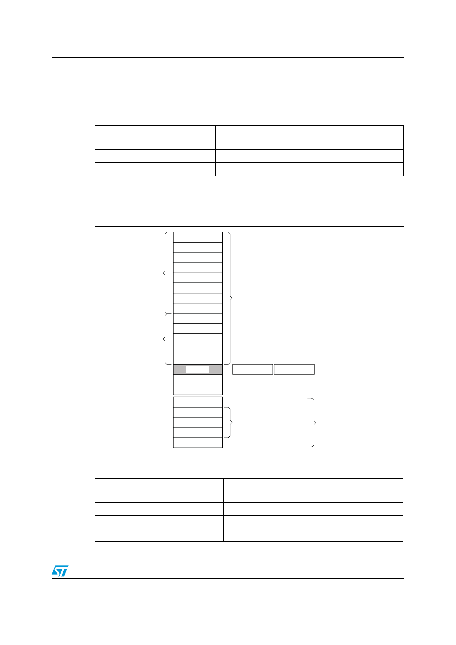
Figure 2.
Processor core registers
Table 1.
Summary of processor mode, execution privilege level, and stack use
options
Processor
mode
Used to
execute
Privilege level for
software execution
Stack used
Thread
Applications
Privileged or unprivileged
(1)
1.
See
.
Main stack or process stack
Handler
Exception handlers
Always privileged
Main stack
Table 2.
Core register set summary
Name
Type
(1)
Required
privilege
(2)
Reset
value
Description
R0-R12
read-write Either
Unknown
General-purpose registers on page 16
MSP
read-write Privileged
See description
PSP
read-write Either
Unknown
SP (R13)
LR (R14)
PC (R15)
R5
R6
R7
R0
R1
R3
R4
R2
R10
R11
R12
R8
R9
Low registers
High registers
MSP
‡
PSP
‡
PSR
PRIMASK
FAULTMASK
BASEPRI
CONTROL
General-purpose registers
Stack Pointer
Link Register
Program Counter
Program status register
Exception mask registers
CONTROL register
Special registers
‡
Banked version of SP
ai15996
The Cortex-M3 processor
PM0056
Doc ID 15491 Rev 3
General-purpose registers
R0-R12 are 32-bit general-purpose registers for data operations.
Stack pointer
The Stack Pointer (SP) is register R13. In Thread mode, bit[1] of the CONTROL register
indicates the stack pointer to use:
●
0 = Main Stack Pointer (MSP). This is the reset value.
●
1 = Process Stack Pointer (PSP).
On reset, the processor loads the MSP with the value from address 0x00000000.
Link register
The Link Register (LR) is register R14. It stores the return information for subroutines,
function calls, and exceptions. On reset, the processor loads the LR value 0xFFFFFFFF.
Program counter
The Program Counter (PC) is register R15. It contains the current program address. Bit[0] is
always 0 because instruction fetches must be halfword aligned. On reset, the processor
loads the PC with the value of the reset vector, which is at address 0x00000004.
LR
read-write Either
0xFFFFFFFF
PC
read-write Either
See description
PSR
read-write Privileged
0x01000000
Program status register on page 17
ASPR
read-write Either
0x00000000
Application program status register on
page 18
IPSR
read-only
Privileged
0x00000000
Interrupt program status register on
page 19
EPSR
read-only
Privileged
0x01000000
Execution program status register on
page 20
PRIMASK
read-write Privileged
0x00000000
Priority mask register on page 21
FAULTMASK
read-write Privileged
0x00000000
Fault mask register on page 21
BASEPRI
read-write Privileged
0x00000000
Base priority mask register on page 22
CONTROL
read-write Privileged
0x00000000
1.
Describes access type during program execution in thread mode and Handler mode. Debug access can
differ.
2.
An entry of Either means privileged and unprivileged software can access the register.
Table 2.
Core register set summary (continued)
Name
Type
(1)
Required
privilege
(2)
Reset
value
Description
PM0056
The Cortex-M3 processor
Doc ID 15491 Rev 3
Program status register
The Program Status Register (PSR) combines:
●
Application Program Status Register (APSR)
●
Interrupt Program Status Register (IPSR)
●
Execution Program Status Register (EPSR)
These registers are mutually exclusive bitfields in the 32-bit PSR. The bit assignments are
as shown in
.
Figure 3.
APSR, IPSR and EPSR bit assignments
Figure 4.
PSR bit assignments
Access these registers individually or as a combination of any two or all three registers,
using the register name as an argument to the MSR or MRS instructions. For example:
●
Read all of the registers using PSR with the MRS instruction
●
Write to the APSR using APSR with the MSR instruction.
The PSR combinations and attributes are:
See the instruction descriptions
for more
information about how to access the program status registers.
Table 3.
PSR register combinations
Register
Type
Combination
PSR
read-write
(1), (2)
1.
The processor ignores writes to the IPSR bits.
2.
Reads of the EPSR bits return zero, and the processor ignores writes to the these bits
APSR, EPSR, and IPSR
IEPSR
read-only
EPSR and IPSR
IAPSR
read-write
APSR and IPSR
EAPSR
read-write
APSR and EPSR
25 24 23
Reserved
ISR_NUMBER
31 30 29 28 27
N Z C V
0
Reserved
APSR
IPSR
EPSR
Reserved
Reserved
26
16 15
10 9
Reserved
ICI/IT
ICI/IT
T
Q
8
N
31 30 29 28 27 26 25 24 23
16 15
10 9 8
0
Z C V Q ICI/IT T
Reserved
ICI/IT
ISR_NUMBER
Reserved

The Cortex-M3 processor
PM0056
Doc ID 15491 Rev 3
Application program status register
The APSR contains the current state of the condition flags from previous instruction
executions. See the register summary in
for its attributes. The bit
assignments are:
Table 4.
APSR bit definitions
Bits
Description
Bit 31
N: Negative or less than flag:
0: Operation result was positive, zero, greater than, or equal
1: Operation result was negative or less than.
Bit 30
Z: Zero flag:
0: Operation result was not zero
1: Operation result was zero.
Bit 29
C: Carry or borrow flag:
0: Add operation did not result in a carry bit or subtract operation resulted in a
borrow bit
1: Add operation resulted in a carry bit or subtract operation did not result in a
borrow bit.
Bit 28
V: Overflow flag:
0: Operation did not result in an overflow
1: Operation resulted in an overflow.
Bit 27
Q: Sticky saturation flag:
0: Indicates that saturation has not occurred since reset or since the bit was last
cleared to zero
1: Indicates when an SSAT or USAT instruction results in saturation.
This bit is cleared to zero by software using an MRS instruction.
Bits 26:0
Reserved.

PM0056
The Cortex-M3 processor
Doc ID 15491 Rev 3
Interrupt program status register
The IPSR contains the exception type number of the current Interrupt Service Routine
(ISR). See the register summary in
for its attributes. The bit assignments
are:
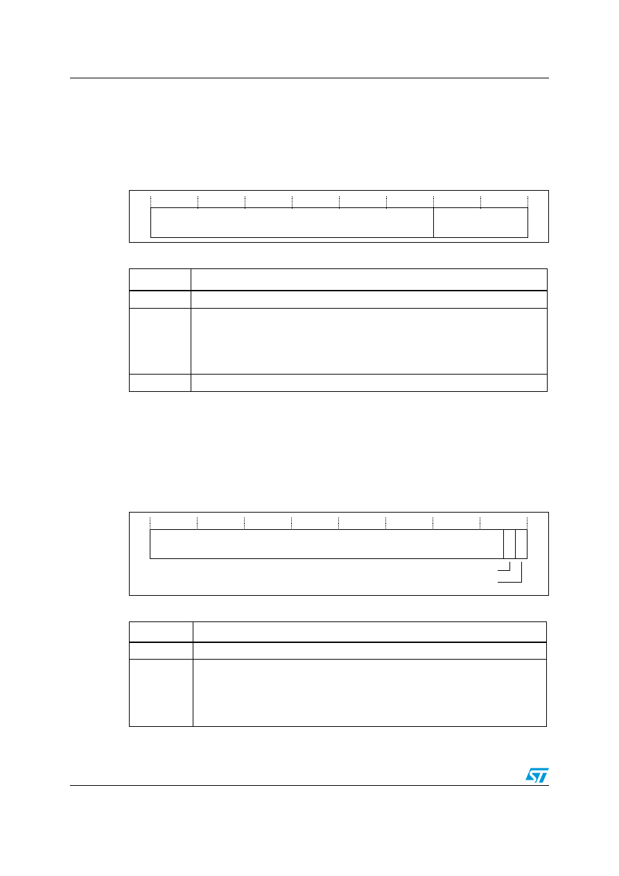
Table 5.
IPSR bit definitions
Bits
Description
Bits 31:9
Reserved
Bits 8:0
ISR_NUMBER:
This is the number of the current exception:
0: Thread mode
1: Reserved
2: NMI
3: Hard fault
4: Memory management fault
5: Bus fault
6: Usage fault
7: Reserved
....
10: Reserved
11: SVCall
12: Reserved for Debug
13: Reserved
14: PendSV
15: SysTick
....
....
83: IRQ67
(1)
see
for more information.
1.
See STM32 product reference manual/datasheet for more information on interrupt mapping
The Cortex-M3 processor
PM0056
Doc ID 15491 Rev 3
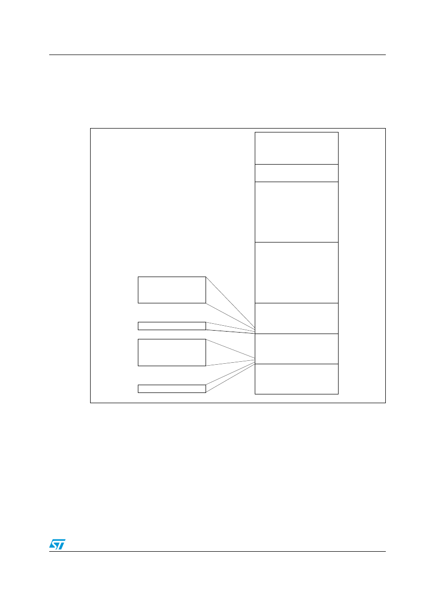
Execution program status register
The EPSR contains the Thumb state bit, and the execution state bits for either the:
●
If-Then (IT) instruction
●
Interruptible-Continuable Instruction (ICI) field for an interrupted load multiple or store
multiple instruction.
See the register summary in
for the EPSR attributes. The bit
assignments are:
Attempts to read the EPSR directly through application software using the MSR instruction
always return zero. Attempts to write the EPSR using the MSR instruction in application
software are ignored. Fault handlers can examine EPSR value in the stacked PSR to
indicate the operation that is at fault. See
Section 2.3.7: Exception entry and return on
Interruptible-continuable instructions
When an interrupt occurs during the execution of an LDM or STM instruction, the processor:
●
Stops the load multiple or store multiple instruction operation temporarily
●
Stores the next register operand in the multiple operation to EPSR bits[15:12].
After servicing the interrupt, the processor:
●
Returns to the register pointed to by bits[15:12]
●
Resumes execution of the multiple load or store instruction.
When the EPSR holds ICI execution state, bits[26:25,11:10] are zero.
If-Then block
The If-Then block contains up to four instructions following a 16-bit IT instruction. Each
instruction in the block is conditional. The conditions for the instructions are either all the
same, or some can be the inverse of others. See
for more information.
Exception mask registers
The exception mask registers disable the handling of exceptions by the processor. Disable
exceptions where they might impact on timing critical tasks.
To access the exception mask registers use the MSR and MRS instructions, or the CPS
instruction to change the value of PRIMASK or FAULTMASK. See
, and
for more information.
Table 6.
EPSR bit definitions
Bits
Description
Bits 31:27
Reserved.
Bits 26:25, 15:10
ICI: Interruptible-continuable instruction bits
See
Interruptible-continuable instructions on page 20
.
Bits 26:25, 15:10
IT: Indicates the execution state bits of the IT instruction, see
Bit 24
Always set to 1.
Bits 23:16
Reserved.
Bits 9:0]
Reserved.
PM0056
The Cortex-M3 processor
Doc ID 15491 Rev 3
Priority mask register
The PRIMASK register prevents activation of all exceptions with configurable priority. See
the register summary in
for its attributes.
shows the bit
assignments.
Figure 5.
PRIMASK bit assignments
Fault mask register
The FAULTMASK register prevents activation of all exceptions except for Non-Maskable
Interrupt (NMI). See the register summary in
for its attributes.
shows the bit assignments.
Figure 6.
FAULTMASK bit assignments
The processor clears the FAULTMASK bit to 0 on exit from any exception handler except the
NMI handler.
Table 7.
PRIMASK register bit definitions
Bits
Description
Bits 31:1
Reserved
Bit 0
PRIMASK:
0: No effect
1: Prevents the activation of all exceptions with configurable priority.
Table 8.
FAULTMASK register bit definitions
Bits
Function
Bits 31:1
Reserved
Bit 0
FAULTMASK:
0: No effect
1: Prevents the activation of all exceptions except for NMI.
31
Reserved
1 0
PRIMASK
Reserved
0
1
31
FAULTMASK
The Cortex-M3 processor
PM0056
Doc ID 15491 Rev 3
Base priority mask register
The BASEPRI register defines the minimum priority for exception processing. When
BASEPRI is set to a nonzero value, it prevents the activation of all exceptions with same or
lower priority level as the BASEPRI value. See the register summary in
for its attributes.
shows the bit assignments.
Figure 7.
BASEPRI bit assignments
CONTROL register
The CONTROL register controls the stack used and the privilege level for software
execution when the processor is in Thread mode. See the register summary in
for its attributes.
shows the bit assignments.
Figure 8.
CONTROL bit assignments
Table 9.
BASEPRI register bit assignments
Bits
Function
Bits 31:8
Reserved
Bits 7:4
BASEPRI[7:4] Priority mask bits
(1)
0x00: no effect
Nonzero: defines the base priority for exception processing.
The processor does not process any exception with a priority value greater than or
equal to BASEPRI.
1.
This field is similar to the priority fields in the interrupt priority registers. See
for more information. Remember that higher priority field values correspond to
lower exception priorities.
Bits 3:0
Reserved
Table 10.
CONTROL register bit definitions
Bits
Function
Bits 31:2
Reserved
Bit 1
ASPSEL: Active stack pointer selection
Selects the current stack:
0: MSP is the current stack pointer
1: PSP is the current stack pointer.
In Handler mode this bit reads as zero and ignores writes.
BASEPRI
Reserved
31
0
7
8
31
2 1 0
Reserved
Active stack pointer
Thread mode privilege level

PM0056
The Cortex-M3 processor
Doc ID 15491 Rev 3
Handler mode always uses the MSP, so the processor ignores explicit writes to the active
stack pointer bit of the CONTROL register when in Handler mode. The exception entry and
return mechanisms update the CONTROL register.
In an OS environment, it is recommended that threads running in Thread mode use the
process stack and the kernel and exception handlers use the main stack.
By default, Thread mode uses the MSP. To switch the stack pointer used in Thread mode to
the PSP, use the MSR instruction to set the Active stack pointer bit to 1, see
.
When changing the stack pointer, software must use an ISB instruction immediately after
the MSR instruction. This ensures that instructions after the ISB execute using the new
stack pointer. See
2.1.4
Exceptions and interrupts
The Cortex-M3 processor supports interrupts and system exceptions. The processor and
the Nested Vectored Interrupt Controller (NVIC) prioritize and handle all exceptions. An
exception changes the normal flow of software control. The processor uses handler mode to
handle all exceptions except for reset. See
and
for more information.
The NVIC registers control interrupt handling. See
Memory protection unit (MPU) on
for more information.
2.1.5 Data
types
The processor:
●
Supports the following data types:
–
32-bit words
–
16-bit halfwords
–
8-bit bytes
●
supports 64-bit data transfer instructions.
●
manages all memory accesses (data memory, instruction memory and Private
Peripheral Bus (PPB)) as little-endian. See
Memory regions, types and attributes on
for more information.
Bit 0
TPL: Thread mode privilege level
Defines the Thread mode privilege level.
0: Privileged
1: Unprivileged.
Table 10.
CONTROL register bit definitions (continued)
Bits
Function

The Cortex-M3 processor
PM0056
Doc ID 15491 Rev 3
2.1.6
The Cortex microcontroller software interface standard (CMSIS)
For a Cortex-M3 microcontroller system, the Cortex Microcontroller Software Interface
Standard (CMSIS) defines:
●
A common way to:
–
Access peripheral registers
–
Define exception vectors
●
The names of:
–
The registers of the core peripherals
–
The core exception vectors
●
A device-independent interface for RTOS kernels, including a debug channel
The CMSIS includes address definitions and data structures for the core peripherals in the
Cortex-M3 processor. It also includes optional interfaces for middleware components
comprising a TCP/IP stack and a Flash file system.
CMSIS simplifies software development by enabling the reuse of template code and the
combination of CMSIS-compliant software components from various middleware vendors.
Software vendors can expand the CMSIS to include their peripheral definitions and access
functions for those peripherals.
This document includes the register names defined by the CMSIS, and gives short
descriptions of the CMSIS functions that address the processor core and the core
peripherals.
This document uses the register short names defined by the CMSIS. In a few cases these
differ from the architectural short names that might be used in other documents.
The following sections give more information about the CMSIS:
●
Section 2.5.4: Power management programming hints on page 45
●
Intrinsic functions on page 51
●
The CMSIS mapping of the Cortex-M3 NVIC registers on page 120
●
PM0056
The Cortex-M3 processor
Doc ID 15491 Rev 3
2.2 Memory
model
This section describes the processor memory map, the behavior of memory accesses, and
the bit-banding features. The processor has a fixed memory map that provides up to 4 GB of
addressable memory.
Figure 9.
Memory map
The regions for SRAM and peripherals include bit-band regions. Bit-banding provides
atomic operations to bit data, see
Section 2.2.5: Bit-banding on page 29
The processor reserves regions of the Private peripheral bus (PPB) address range for core
peripheral registers, see
Section 4.1: About the STM32 core peripherals on page 106
.
Vendor-specific
memory
External device
External RAM
Peripheral
SRAM
Code
0xFFFFFFFF
Private peripheral
bus
0xE0100000
0xE00FFFFF
0x9FFFFFFF
0xA0000000
0x5FFFFFFF
0x60000000
0x3FFFFFFF
0x40000000
0x1FFFFFFF
0x20000000
0x00000000
0x40000000
Bit band region
Bit band alias
32MB
1MB
0x400FFFFF
0x42000000
0x43FFFFFF
Bit band region
Bit band alias
32MB
1MB
0x20000000
0x200FFFFF
0x22000000
0x23FFFFFF
1.0GB
1.0GB
0.5GB
0.5GB
0.5GB
0xDFFFFFFF
0xE0000000
1.0MB
511MB

The Cortex-M3 processor
PM0056
Doc ID 15491 Rev 3
2.2.1
Memory regions, types and attributes
The memory map splits the memory map into regions. Each region has a defined memory
type, and some regions have additional memory attributes. The memory type and attributes
determine the behavior of accesses to the region.
The memory types are:
The different ordering requirements for Device and Strongly-ordered memory mean that the
memory system can buffer a write to Device memory, but must not buffer a write to Strongly-
ordered memory.
The additional memory attributes include:
Normal
The processor can re-order transactions for efficiency, or
perform speculative reads.
Device
The processor preserves transaction order relative to other
transactions to Device or Strongly-ordered memory.
Strongly-ordered
The processor preserves transaction order relative to all other
transactions.
Execute Never (XN)
Means the processor prevents instruction accesses. Any
attempt to fetch an instruction from an XN region causes a
memory management fault exception.
PM0056
The Cortex-M3 processor
Doc ID 15491 Rev 3
2.2.2 Memory
system
ordering of memory accesses
For most memory accesses caused by explicit memory access instructions, the memory
system does not guarantee that the order in which the accesses complete matches the
program order of the instructions, providing this does not affect the behavior of the
instruction sequence. Normally, if correct program execution depends on two memory
accesses completing in program order, software must insert a memory barrier instruction
between the memory access instructions, see
Section 2.2.4: Software ordering of memory
However, the memory system does guarantee some ordering of accesses to Device and
Strongly-ordered memory. For two memory access instructions A1 and A2, if A1 occurs
before A2 in program order, the ordering of the memory accesses caused by two
instructions is:
2.2.3
Behavior of memory accesses
The behavior of accesses to each region in the memory map is:
Table 11.
Ordering of memory accesses
(1)
1.
- means that the memory system does not guarantee the ordering of the accesses.
< means that accesses are observed in program order, that is, A1 is always observed before A2.
A1
A2
Normal access
Device access
Strongly ordered
access
Non-shareable
Shareable
Normal access
-
-
-
-
Device access, non-
shareable
-
<
-
<
Device access, shareable
-
-
<
<
Strongly ordered access
-
<
<
<
Table 12.
Memory access behavior
Address
range
Memory
region
Memory
type
XN
Description
0x00000000- 0x1FFFFFFF
Code
Normal
(1)
-
Executable region for program code.
You can also put data here.
0x20000000- 0x3FFFFFFF
SRAM
Normal
-
Executable region for data. You can
also put code here.
This region includes bit band and bit
band alias areas, see
.
0x40000000- 0x5FFFFFFF
Peripheral
Device
XN
This region includes bit band and bit
band alias areas, see
.
0x60000000- 0x9FFFFFFF
External
RAM
Normal
-
Executable region for data.

The Cortex-M3 processor
PM0056
Doc ID 15491 Rev 3
The Code, SRAM, and external RAM regions can hold programs. However, it is
recommended that programs always use the Code region. This is because the processor
has separate buses that enable instruction fetches and data accesses to occur
simultaneously.
2.2.4
Software ordering of memory accesses
The order of instructions in the program flow does not always guarantee the order of the
corresponding memory transactions. This is because:
●
The processor can reorder some memory accesses to improve efficiency, providing this
does not affect the behavior of the instruction sequence.
●
The processor has multiple bus interfaces
●
Memory or devices in the memory map have different wait states
●
Some memory accesses are buffered or speculative.
Section 2.2.2: Memory system ordering of memory accesses on page 27
describes the
cases where the memory system guarantees the order of memory accesses. Otherwise, if
the order of memory accesses is critical, software must include memory barrier instructions
to force that ordering. The processor provides the following memory barrier instructions:
Use memory barrier instructions in, for example:
●
Vector table. If the program changes an entry in the vector table, and then enables the
corresponding exception, use a DMB instruction between the operations. This ensures
that if the exception is taken immediately after being enabled the processor uses the
new exception vector.
0xA0000000- 0xDFFFFFFF
External
device
Device
XN
External Device memory
0xE0000000- 0xE00FFFFF
Private
Peripheral
Bus
Strongly-
ordered
XN
This region includes the NVIC,
System timer, and system control
block.
0xE0100000- 0xFFFFFFFF
Memory
mapped
peripherals
Device
XN
This region includes all the STM32
standard peripherals.
1.
See
Memory regions, types and attributes on page 26
for more information.
Table 12.
Memory access behavior (continued)
Address
range
Memory
region
Memory
type
XN
Description
DMB
The Data Memory Barrier (DMB) instruction ensures that outstanding
memory transactions complete before subsequent memory transactions.
See
.
DSB
The Data Synchronization Barrier (DSB) instruction ensures that
outstanding memory transactions complete before subsequent
instructions execute. See
ISB
The Instruction Synchronization Barrier (ISB) ensures that the effect of all
completed memory transactions is recognizable by subsequent
instructions. See
.

PM0056
The Cortex-M3 processor
Doc ID 15491 Rev 3
●
Self-modifying code. If a program contains self-modifying code, use an ISB
instruction immediately after the code modification in the program. This ensures
subsequent instruction execution uses the updated program.
●
Memory map switching. If the system contains a memory map switching mechanism,
use a DSB instruction after switching the memory map in the program. This ensures
subsequent instruction execution uses the updated memory map.
●
Dynamic exception priority change. When an exception priority has to change when
the exception is pending or active, use DSB instructions after the change. This ensures
the change takes effect on completion of the DSB instruction.
●
Using a semaphore in multi-master system. If the system contains more than one
bus master, for example, if another processor is present in the system, each processor
must use a DMB instruction after any semaphore instructions, to ensure other bus
masters see the memory transactions in the order in which they were executed.
Memory accesses to Strongly-ordered memory, such as the system control block, do not
require the use of DMB instructions.
2.2.5 Bit-banding
A bit-band region maps each word in a bit-band alias region to a single bit in the bit-band
region. The bit-band regions occupy the lowest 1 MB of the SRAM and peripheral memory
regions.
The memory map has two 32 MB alias regions that map to two 1 MB bit-band regions:
●
Accesses to the 32 MB SRAM alias region map to the 1 MB SRAM bit-band region, as
shown in
●
Accesses to the 32 MB peripheral alias region map to the 1 MB peripheral bit-band
region, as shown in
.
A word access to the SRAM or peripheral bit-band alias regions map to a single bit in the
SRAM or peripheral bit-band region.
Table 13.
SRAM memory bit-banding regions
Address
range
Memory
region
Instruction and data accesses
0x20000000-
0x200FFFFF
SRAM bit-band region
Direct accesses to this memory range behave as SRAM memory
accesses, but this region is also bit addressable through bit-band alias.
0x22000000-
0x23FFFFFF
SRAM bit-band alias
Data accesses to this region are remapped to bit band region. A write
operation is performed as read-modify-write. Instruction accesses are not
remapped.
Table 14.
Peripheral memory bit-banding regions
Address
range
Memory
region
Instruction and data accesses
0x40000000-
0x400FFFFF
Peripheral
bit-band region
Direct accesses to this memory range behave as peripheral memory
accesses, but this region is also bit addressable through bit-band
alias.
0x42000000-
0x43FFFFFF
Peripheral
bit-band alias
Data accesses to this region are remapped to bit-band region. A write
operation is performed as read-modify-write. Instruction accesses are
not permitted.
The Cortex-M3 processor
PM0056
Doc ID 15491 Rev 3
The following formula shows how the alias region maps onto the bit-band region:
bit_word_offset = (byte_offset x 32) + (bit_number x 4)
bit_word_addr = bit_band_base + bit_word_offset
Where:
●
Bit_word_offset is the position of the target bit in the bit-band memory region.
●
Bit_word_addr is the address of the word in the alias memory region that maps to the
targeted bit.
●
Bit_band_base is the starting address of the alias region.
●
Byte_offset is the number of the byte in the bit-band region that contains the targeted
bit.
●
Bit_number is the bit position, 0-7, of the targeted bit.
shows examples of bit-band mapping between the SRAM bit-band
alias region and the SRAM bit-band region:
●
The alias word at 0x23FFFFE0 maps to bit[0] of the bit-band byte at
0x200FFFFF: 0x23FFFFE0 = 0x22000000 + (0xFFFFF*32) + (0*4).
●
The alias word at 0x23FFFFFC maps to bit[7] of the bit-band byte at
0x200FFFFF: 0x23FFFFFC = 0x22000000 + (0xFFFFF*32) + (7*4).
●
The alias word at 0x22000000 maps to bit[0] of the bit-band byte at
0x20000000: 0x22000000 = 0x22000000 + (0*32) + (0 *4).
●
The alias word at 0x2200001C maps to bit[7] of the bit-band byte at
0x20000000: 0x2200001C = 0x22000000+ (0*32) + (7*4).
Figure 10.
Bit-band mapping
Directly accessing an alias region
Writing to a word in the alias region updates a single bit in the bit-band region.
0x23FFFFE4
0x22000004
0x23FFFFE0
0x23FFFFE8
0x23FFFFEC
0x23FFFFF0
0x23FFFFF4
0x23FFFFF8
0x23FFFFFC
0x22000000
0x22000014
0x22000018
0x2200001C
0x22000008
0x22000010
0x2200000C
32MB alias region
0
7
0
0
7
0x20000000
0x20000001
0x20000002
0x20000003
6
5
4
3
2
1
0
7
6
5
4
3
2
1
7
6
5
4
3
2
1
0
7
6
5
4
3
2
1
0
7
6
5
4
3
2
1
6
5
4
3
2
1
0
7
6
5
4
3
2
1
0
7
6
5
4
3
2
1
0x200FFFFC
0x200FFFFD
0x200FFFFE
0x200FFFFF
1MB SRAM bit-band region
PM0056
The Cortex-M3 processor
Doc ID 15491 Rev 3
Bit[0] of the value written to a word in the alias region determines the value written to the
targeted bit in the bit-band region. Writing a value with bit[0] set to 1 writes a 1 to the bit-
band bit, and writing a value with bit[0] set to 0 writes a 0 to the bit-band bit.
Bits[31:1] of the alias word have no effect on the bit-band bit. Writing 0x01 has the same
effect as writing 0xFF. Writing 0x00 has the same effect as writing 0x0E.
Reading a word in the alias region:
●
0x00000000 indicates that the targeted bit in the bit-band region is set to zero
●
0x00000001 indicates that the targeted bit in the bit-band region is set to 1
Directly accessing a bit-band region
Behavior of memory accesses on page 27
describes the behavior of direct byte, halfword, or
word accesses to the bit-band regions.
2.2.6 Memory
endianness
The processor views memory as a linear collection of bytes numbered in ascending order
from zero. For example, bytes 0-3 hold the first stored word, and bytes 4-7 hold the second
stored word.
Little-endian format
In little-endian format, the processor stores the least significant byte of a word at the lowest-
numbered byte, and the most significant byte at the highest-numbered byte. See
for an example.
Figure 11.
Little-endian example
Memory
Register
Address A
A+1
lsbyte
msbyte
A+2
A+3
0
7
B0
B1
B3
B2
31
24 23
16 15
8 7
0
B0
B1
B2
B3

The Cortex-M3 processor
PM0056
Doc ID 15491 Rev 3
2.2.7 Synchronization
primitives
The Cortex-M3 instruction set includes pairs of synchronization primitives. These provide a
non-blocking mechanism that a thread or process can use to obtain exclusive access to a
memory location. Software can use them to perform a guaranteed read-modify-write
memory update sequence, or for a semaphore mechanism.
A pair of synchronization primitives comprises:
The pairs of Load-Exclusive and Store-Exclusive instructions are:
●
The word instructions LDREX and STREX
●
The halfword instructions LDREXH and STREXH
●
The byte instructions LDREXB and STREXB.
Software must use a Load-Exclusive instruction with the corresponding Store-Exclusive
instruction.
To perform a guaranteed read-modify-write of a memory location, software must:
1.
Use a Load-Exclusive instruction to read the value of the location.
2.
Update the value, as required.
3.
Use a Store-Exclusive instruction to attempt to write the new value back to the memory
location, and tests the returned status bit. If this bit is:
0: The read-modify-write completed successfully,
1: No write was performed. This indicates that the value returned at step 1 might
be out of date. The software must retry the read-modify-write sequence,
A Load-Exclusive instruction
Used to read the value of a memory location, requesting
exclusive access to that location.
A Store-Exclusive instruction
Used to attempt to write to the same memory location,
returning a status bit to a register. If this bit is:
0: it indicates that the thread or process gained
exclusive access to the memory, and the write
succeeds
1: it indicates that the thread or process did not gain
exclusive access to the memory, and no write is
performed
PM0056
The Cortex-M3 processor
Doc ID 15491 Rev 3
Software can use the synchronization primitives to implement a semaphores as follows:
1.
Use a Load-Exclusive instruction to read from the semaphore address to check
whether the semaphore is free.
2.
If the semaphore is free, use a Store-Exclusive to write the claim value to the
semaphore address.
3.
If the returned status bit from step 2 indicates that the Store-Exclusive succeeded then
the software has claimed the semaphore. However, if the Store-Exclusive failed,
another process might have claimed the semaphore after the software performed step
1.
The Cortex-M3 includes an exclusive access monitor, that tags the fact that the processor
has executed a Load-Exclusive instruction.
The processor removes its exclusive access tag if:
●
It executes a CLREX instruction
●
It executes a Store-Exclusive instruction, regardless of whether the write succeeds.
●
An exception occurs. This means the processor can resolve semaphore conflicts
between different threads.
For more information about the synchronization primitive instructions, see
2.2.8
Programming hints for the synchronization primitives
ANSI C cannot directly generate the exclusive access instructions. Some C compilers
provide intrinsic functions for generation of these instructions:
The actual exclusive access instruction generated depends on the data type of the pointer
passed to the intrinsic function. For example, the following C code generates the require
LDREXB operation:
__ldrex((volatile char *) 0xFF);
Table 15.
C compiler intrinsic functions for exclusive access instructions
Instruction
Intrinsic function
LDREX, LDREXH, or LDREXB
unsigned int __ldrex(volatile void *ptr)
STREX, STREXH, or STREXB
int __strex(unsigned int val, volatile void *ptr)
CLREX
void __clrex(void)

The Cortex-M3 processor
PM0056
Doc ID 15491 Rev 3
2.3 Exception
model
This section describes the exception model.
2.3.1 Exception
states
Each exception is in one of the following states:
2.3.2 Exception
types
The exception types are:
Inactive
The exception is not active and not pending.
Pending
The exception is waiting to be serviced by the processor. An
interrupt request from a peripheral or from software can change
the state of the corresponding interrupt to pending.
Active
An exception that is being serviced by the processor but has not
completed.
Note: An exception handler can interrupt the execution of another
exception handler. In this case both exceptions are in the active
state.
Active and pending
The exception is being serviced by the processor and there is a
pending exception from the same source.
Reset
Reset is invoked on power up or a warm reset. The exception model
treats reset as a special form of exception. When reset is asserted,
the operation of the processor stops, potentially at any point in an
instruction. When reset is deasserted, execution restarts from the
address provided by the reset entry in the vector table. Execution
restarts as privileged execution in Thread mode.
NMI A
NonMaskable Interrupt (NMI) can be signalled by a peripheral or
triggered by software. This is the highest priority exception other
than reset. It is permanently enabled and has a fixed priority of -2.
NMIs cannot be:
●
Masked or prevented from activation by any other exception
●
Preempted by any exception other than Reset.
Hard fault
A hard fault is an exception that occurs because of an error during
exception processing, or because an exception cannot be managed
by any other exception mechanism. Hard faults have a fixed priority
of -1, meaning they have higher priority than any exception with
configurable priority.
Memory management
fault
A memory management fault is an exception that occurs because of
a memory protection related fault. The fixed memory protection
constraints determines this fault, for both instruction and data
memory transactions. This fault is used to abort instruction accesses
to Execute Never (XN) memory regions.

PM0056
The Cortex-M3 processor
Doc ID 15491 Rev 3
Bus fault
A bus fault is an exception that occurs because of a memory related
fault for an instruction or data memory transaction. This might be
from an error detected on a bus in the memory system.
Usage fault
A usage fault is an exception that occurs because of a fault related to
instruction execution. This includes:
●
An undefined instruction
●
An illegal unaligned access
●
Invalid state on instruction execution
●
An error on exception return.
The following can cause a usage fault when the core is configured to
report them:
●
An unaligned address on word and halfword memory access
●
Division by zero
SVCall A
supervisor call (SVC) is an exception that is triggered by the SVC
instruction. In an OS environment, applications can use SVC
instructions to access OS kernel functions and device drivers.
PendSV
PendSV is an interrupt-driven request for system-level service. In an
OS environment, use PendSV for context switching when no other
exception is active.
SysTick
A SysTick exception is an exception the system timer generates
when it reaches zero. Software can also generate a SysTick
exception. In an OS environment, the processor can use this
exception as system tick.
Interrupt (IRQ)
A interrupt, or IRQ, is an exception signalled by a peripheral, or
generated by a software request. All interrupts are asynchronous to
instruction execution. In the system, peripherals use interrupts to
communicate with the processor.
Table 16.
Properties of the different exception types
Exception
number
(1)
IRQ
number
Exception
type
Priority
Vector address
or offset
(2)
Activation
1
-
Reset
-3, the highest
0x00000004
Asynchronous
2
-14
NMI
-2
0x00000008
Asynchronous
3
-13
Hard fault
-1
0x0000000C
-
4 -12
Memory
management fault
Configurable
(3)
0x00000010
Synchronous
5
-11
Bus fault
Configurable
0x00000014
Synchronous when precise,
asynchronous when imprecise
6
-10
Usage fault
Configurable
0x00000018
Synchronous
7-10
-
-
-
Reserved
-
11
-5
SVCall
Configurable
0x0000002C
Synchronous
12-13
-
-
-
Reserved
-

The Cortex-M3 processor
PM0056
Doc ID 15491 Rev 3
For an asynchronous exception, other than reset, the processor can execute another
instruction between when the exception is triggered and when the processor enters the
exception handler.
Privileged software can disable the exceptions that
shows as having
configurable priority, see:
●
System handler control and state register (SCB_SHCSR) on page 139
●
Interrupt clear-enable registers (NVIC_ICERx) on page 122
For more information about hard faults, memory management faults, bus faults, and usage
faults, see
Section 2.4: Fault handling on page 41
2.3.3 Exception
handlers
The processor handles exceptions using:
14
-2
PendSV
Configurable
0x00000038
Asynchronous
15
-1
SysTick
Configurable
0x0000003C Asynchronous
16-83
0-67
Interrupt (IRQ)
Configurable
(4)
0x00000040 and
above
(5)
Asynchronous
1.
To simplify the software layer, the CMSIS only uses IRQ numbers and therefore uses negative values for exceptions other
than interrupts. The IPSR returns the Exception number, see
Interrupt program status register on page 19
.
2.
See
for more information.
3.
See
System handler priority registers (SHPRx) on page 137
.
4.
See
Interrupt priority registers (NVIC_IPRx) on page 126
5.
Increasing in steps of 4.
Table 16.
Properties of the different exception types (continued)
Exception
number
(1)
IRQ
number
(1)
Exception
type
Priority
Vector address
or offset
(2)
Activation
Interrupt Service
Routines (ISRs)
Interrupts IRQ0 to IRQ67 are the exceptions handled by ISRs.
Fault handlers
Hard fault, memory management fault, usage fault, bus fault are fault
exceptions handled by the fault handlers.
System handlers
NMI, PendSV, SVCall SysTick, and the fault exceptions are all
system exceptions that are handled by system handlers.
PM0056
The Cortex-M3 processor
Doc ID 15491 Rev 3
2.3.4 Vector
table
The vector table contains the reset value of the stack pointer, and the start addresses, also
called exception vectors, for all exception handlers.
shows the order of
the exception vectors in the vector table. The least-significant bit of each vector must be 1,
indicating that the exception handler is Thumb code.
Figure 12.
Vector table
On system reset, the vector table is fixed at address 0x00000000. Privileged software can
write to the VTOR to relocate the vector table start address to a different memory location, in
the range 0x00000080 to 0x3FFFFF80, see
Vector table offset register (SCB_VTOR) on
.
2.3.5 Exception
priorities
As
shows, all exceptions have an associated priority, with:
●
A lower priority value indicating a higher priority
●
Configurable priorities for all exceptions except Reset, Hard fault, and NMI.
Initial SP value
Reset
Hard fault
NMI
Memory management fault
Usage fault
Bus fault
0x0000
0x0004
0x0008
0x000C
0x0010
0x0014
0x0018
Reserved
SVCall
PendSV
Reserved for Debug
Systick
IRQ0
Reserved
0x002C
0x0038
0x003C
0x0040
Offset
Exception number
2
3
4
5
6
11
12
14
15
16
18
13
7
10
1
Vector
.
.
.
8
9
IRQ1
IRQ2
0x0044
IRQ67
17
0x0048
0x004C
83
.
.
.
.
.
.
0x014C
IRQ number
-14
-13
-12
-11
-10
-5
-2
-1
0
2
1
67
ai15995

The Cortex-M3 processor
PM0056
Doc ID 15491 Rev 3
If software does not configure any priorities, then all exceptions with a configurable priority
have a priority of 0. For information about configuring exception priorities see
●
System handler priority registers (SHPRx) on page 137
●
Interrupt priority registers (NVIC_IPRx) on page 126
Configurable priority values are in the range 0-15. This means that the Reset, Hard fault,
and NMI exceptions, with fixed negative priority values, always have higher priority than any
other exception.
For example, assigning a higher priority value to IRQ[0] and a lower priority value to IRQ[1]
means that IRQ[1] has higher priority than IRQ[0]. If both IRQ[1] and IRQ[0] are asserted,
IRQ[1] is processed before IRQ[0].
If multiple pending exceptions have the same priority, the pending exception with the lowest
exception number takes precedence. For example, if both IRQ[0] and IRQ[1] are pending
and have the same priority, then IRQ[0] is processed before IRQ[1].
When the processor is executing an exception handler, the exception handler is preempted
if a higher priority exception occurs. If an exception occurs with the same priority as the
exception being handled, the handler is not preempted, irrespective of the exception
number. However, the status of the new interrupt changes to pending.
2.3.6
Interrupt priority grouping
To increase priority control in systems with interrupts, the NVIC supports priority grouping.
This divides each interrupt priority register entry into two fields:
●
An upper field that defines the group priority
●
A lower field that defines a subpriority within the group.
Only the group priority determines preemption of interrupt exceptions. When the processor
is executing an interrupt exception handler, another interrupt with the same group priority as
the interrupt being handled does not preempt the handler,
If multiple pending interrupts have the same group priority, the subpriority field determines
the order in which they are processed. If multiple pending interrupts have the same group
priority and subpriority, the interrupt with the lowest IRQ number is processed first.
For information about splitting the interrupt priority fields into group priority and subpriority,
see
Application interrupt and reset control register (SCB_AIRCR) on page 134
.
2.3.7
Exception entry and return
Descriptions of exception handling use the following terms:
Preemption
When the processor is executing an exception handler, an exception
can preempt the exception handler if its priority is higher than the
priority of the exception being handled. See
for more information about preemption by an
interrupt.
When one exception preempts another, the exceptions are called
nested exceptions. See
more
information.

PM0056
The Cortex-M3 processor
Doc ID 15491 Rev 3
Exception entry
Exception entry occurs when there is a pending exception with sufficient priority and either:
●
The processor is in Thread mode
●
The new exception is of higher priority than the exception being handled, in which case
the new exception preempts the original exception.
When one exception preempts another, the exceptions are nested.
Sufficient priority means the exception has more priority than any limits set by the mask
registers, see
Exception mask registers on page 20
. An exception with less priority than this
is pending but is not handled by the processor.
When the processor takes an exception, unless the exception is a tail-chained or a late-
arriving exception, the processor pushes information onto the current stack. This operation
is referred as stacking and the structure of eight data words is referred as stack frame. The
stack frame contains the following information:
●
R0-R3, R12
●
Return address
●
PSR
●
LR.
Immediately after stacking, the stack pointer indicates the lowest address in the stack frame.
Unless stack alignment is disabled, the stack frame is aligned to a double-word address. If
the STKALIGN bit of the Configuration Control Register (CCR) is set to 1, stack align
adjustment is performed during stacking.
Return
This occurs when the exception handler is completed, and:
●
There is no pending exception with sufficient priority to be
serviced
●
The completed exception handler was not handling a late-
arriving exception.
The processor pops the stack and restores the processor state to the
state it had before the interrupt occurred. See
for more information.
Tail-chaining
This mechanism speeds up exception servicing. On completion of an
exception handler, if there is a pending exception that meets the
requirements for exception entry, the stack pop is skipped and
control transfers to the new exception handler.
Late-arriving
This mechanism speeds up preemption. If a higher priority exception
occurs during state saving for a previous exception, the processor
switches to handle the higher priority exception and initiates the
vector fetch for that exception. State saving is not affected by late
arrival because the state saved is the same for both exceptions.
Therefore the state saving continues uninterrupted. The processor
can accept a late arriving exception until the first instruction of the
exception handler of the original exception enters the execute stage
of the processor. On return from the exception handler of the late-
arriving exception, the normal tail-chaining rules apply.
The Cortex-M3 processor
PM0056
Doc ID 15491 Rev 3
The stack frame includes the return address. This is the address of the next instruction in
the interrupted program. This value is restored to the PC at exception return so that the
interrupted program resumes.
In parallel to the stacking operation, the processor performs a vector fetch that reads the
exception handler start address from the vector table. When stacking is complete, the
processor starts executing the exception handler. At the same time, the processor writes an
EXC_RETURN value to the LR. This indicates which stack pointer corresponds to the stack
frame and what operation mode the was processor was in before the entry occurred.
If no higher priority exception occurs during exception entry, the processor starts executing
the exception handler and automatically changes the status of the corresponding pending
interrupt to active.
If another higher priority exception occurs during exception entry, the processor starts
executing the exception handler for this exception and does not change the pending status
of the earlier exception. This is the late arrival case.
Exception return
Exception return occurs when the processor is in Handler mode and executes one of the
following instructions to load the EXC_RETURN value into the PC:
●
A POP instruction that includes the PC
●
A BX instruction with any register.
●
An LDR or LDM instruction with the PC as the destination
EXC_RETURN is the value loaded into the LR on exception entry. The exception
mechanism relies on this value to detect when the processor has completed an exception
handler. The lowest four bits of this value provide information on the return stack and
processor mode.
shows the EXC_RETURN[3:0] values with a description of the
exception return behavior.
The processor sets EXC_RETURN bits[31:4] to 0xFFFFFFF. When this value is loaded into
the PC it indicates to the processor that the exception is complete, and the processor
initiates the exception return sequence.
Table 17.
Exception return behavior
EXC_RETURN[3:0]
Description
0bxxx0
Reserved.
0b0001
Return to Handler mode.
Exception return gets state from MSP.
Execution uses MSP after return.
0b0011
Reserved.
0b01x1
Reserved.
0b1001
Return to Thread mode.
Exception return gets state from MSP.
Execution uses MSP after return.
PM0056
The Cortex-M3 processor
Doc ID 15491 Rev 3
2.4 Fault
handling
Faults are a subset of the exceptions, see
. The following
generate a fault:
●
A bus error on:
–
An instruction fetch or vector table load
–
A data access
●
An internally-detected error such as an undefined instruction or an attempt to change
state with a BX instruction
●
Attempting to execute an instruction from a memory region marked as Non-Executable
(XN).
2.4.1 Fault
types
shows the types of fault, the handler used for the fault, the corresponding fault
status register, and the register bit that indicates that the fault has occurred. See
Configurable fault status register (SCB_CFSR) on page 141
for more information about the
fault status registers.
0b1101
Return to Thread mode.
Exception return gets state from PSP.
Execution uses PSP after return.
0b1x11
Reserved.
Table 17.
Exception return behavior (continued)
EXC_RETURN[3:0]
Description
Table 18.
Faults
Fault
Handler
Bit name
Fault status register
Bus error on a vector read
Hard fault
VECTTBL
Hard fault status register
(SCB_HFSR) on page 144
Fault escalated to a hard fault
FORCED
Bus error:
Bus fault
-
-
During exception stacking
STKERR
Configurable fault status
register (SCB_CFSR) on
page 141
During exception unstacking
UNSTKERR
During instruction prefetch
IBUSERR
Precise data bus error
PRECISERR
Imprecise data bus error
IMPRECISERR

The Cortex-M3 processor
PM0056
Doc ID 15491 Rev 3
2.4.2 Fault
escalation and hard faults
All faults exceptions except for hard fault have configurable exception priority, see
handler priority registers (SHPRx) on page 137
. Software can disable execution of the
handlers for these faults, see
System handler control and state register (SCB_SHCSR) on
.
Usually, the exception priority, together with the values of the exception mask registers,
determines whether the processor enters the fault handler, and whether a fault handler can
preempt another fault handler. as described in
Section 2.3: Exception model on page 34
.
In some situations, a fault with configurable priority is treated as a hard fault. This is called
priority escalation, and the fault is described as escalated to hard fault. Escalation to hard
fault occurs when:
●
A fault handler causes the same kind of fault as the one it is servicing. This escalation
to hard fault occurs because a fault handler cannot preempt itself because it must have
the same priority as the current priority level.
●
A fault handler causes a fault with the same or lower priority as the fault it is servicing.
This is because the handler for the new fault cannot preempt the currently executing
fault handler.
●
An exception handler causes a fault for which the priority is the same as or lower than
the currently executing exception.
●
A fault occurs and the handler for that fault is not enabled.
If a bus fault occurs during a stack push when entering a bus fault handler, the bus fault
does not escalate to a hard fault. This means that if a corrupted stack causes a fault, the
fault handler executes even though the stack push for the handler failed. The fault handler
operates but the stack contents are corrupted.
Only Reset and NMI can preempt the fixed priority hard fault. A hard fault can preempt any
exception other than Reset, NMI, or another hard fault.
Attempt to access a coprocessor
Usage fault
NOCP
Configurable fault status
register (SCB_CFSR) on
page 141
Undefined instruction
UNDEFINSTR
Attempt to enter an invalid instruction
set state
(1)
INVSTATE
Invalid EXC_RETURN value
INVPC
Illegal unaligned load or store
UNALIGNED
Divide By 0
DIVBYZERO
1.
Attempting to use an instruction set other than the Thumb instruction set.
Table 18.
Faults (continued)
Fault
Handler
Bit name
Fault status register

PM0056
The Cortex-M3 processor
Doc ID 15491 Rev 3
2.4.3 Fault
status
registers and fault address registers
The fault status registers indicate the cause of a fault. For bus faults and memory
management faults, the fault address register indicates the address accessed by the
operation that caused the fault, as shown in
2.4.4 Lockup
The processor enters a lockup state if a hard fault occurs when executing the NMI or hard
fault handlers. When the processor is in lockup state it does not execute any instructions.
The processor remains in lockup state until either:
●
It is reset
●
An NMI occurs
If lockup state occurs from the NMI handler a subsequent NMI does not cause the processor
to leave lockup state.
2.5 Power
management
The STM32 and Cortex-M3 processor sleep modes reduce power consumption:
●
Sleep mode stops the processor clock. All other system and peripheral clocks may still
be running.
●
Deep sleep mode stops most of the STM32 system and peripheral clocks. At product
level, this corresponds to either the Stop or the Standby mode. For more details, please
refer to the “Power modes” Section in the STM32 reference manual.
The SLEEPDEEP bit of the SCR selects which sleep mode is used, see
register (SCB_SCR) on page 135
. For more information about the behavior of the sleep
modes see the STM32 product reference manual.
This section describes the mechanisms for entering sleep mode, and the conditions for
waking up from sleep mode.
Table 19.
Fault status and fault address registers
Handler
Status register
name
Address register
name
Register description
Hard fault
HFSR
-
Hard fault status register (SCB_HFSR) on
page 144
Memory
management fault
MMFSR
MMFAR
Configurable fault status register (SCB_CFSR)
on page 141
Memory management fault address register
(SCB_MMFAR) on page 146
Bus fault
BFSR
BFAR
Configurable fault status register (SCB_CFSR)
on page 141
Bus fault address register (SCB_BFAR) on
page 146
Usage fault
UFSR
-

The Cortex-M3 processor
PM0056
Doc ID 15491 Rev 3
2.5.1 Entering
sleep
mode
This section describes the mechanisms software can use to put the processor into sleep
mode.
The system can generate spurious wakeup events, for example a debug operation wakes up
the processor. Therefore software must be able to put the processor back into sleep mode
after such an event. A program might have an idle loop to put the processor back to sleep
mode.
Wait for interrupt
The wait for interrupt instruction, WFI, causes immediate entry to sleep mode. When the
processor executes a WFI instruction it stops executing instructions and enters sleep mode.
See
Wait for event
The wait for event instruction, WFE, causes entry to sleep mode conditional on the value of
an one-bit event register. When the processor executes a WFE instruction, it checks this
register:
●
If the register is 0 the processor stops executing instructions and enters sleep mode
●
If the register is 1 the processor clears the register to 0 and continues executing
instructions without entering sleep mode.
See
for more information.
If the event register is 1, this indicate that the processor must not enter sleep mode on
execution of a WFE instruction. Typically, this is because an external event signal is
asserted, or a processor in the system has executed an SEV instruction, see
. Software cannot access this register directly.
Sleep-on-exit
If the SLEEPONEXIT bit of the SCR is set to 1, when the processor completes the execution
of an exception handler it returns to Thread mode and immediately enters sleep mode. Use
this mechanism in applications that only require the processor to run when an exception
occurs.
2.5.2
Wakeup from sleep mode
The conditions for the processor to wakeup depend on the mechanism that cause it to enter
sleep mode.
Wakeup from WFI or sleep-on-exit
Normally, the processor wakes up only when it detects an exception with sufficient priority to
cause exception entry.
Some embedded systems might have to execute system restore tasks after the processor
wakes up, and before it executes an interrupt handler. To achieve this set the PRIMASK bit
to 1 and the FAULTMASK bit to 0. If an interrupt arrives that is enabled and has a higher
priority than current exception priority, the processor wakes up but does not execute the
interrupt handler until the processor sets PRIMASK to zero. For more information about
PRIMASK and FAULTMASK see
Exception mask registers on page 20
.

PM0056
The Cortex-M3 processor
Doc ID 15491 Rev 3
Wakeup from WFE
The processor wakes up if:
●
it detects an exception with sufficient priority to cause exception entry
●
it detects an external event signal, see
The external event input on page 45
In addition, if the SEVONPEND bit in the SCR is set to 1, any new pending interrupt triggers
an event and wakes up the processor, even if the interrupt is disabled or has insufficient
priority to cause exception entry. For more information about the SCR see
register (SCB_SCR) on page 135
.
2.5.3
The external event input
The processor provides an external event input signal. This signal can be generated by the
up to 16 external input lines, by the PVD, RTC alarm or by the USB wakeup event,
configured through the external interrupt/event controller (EXTI).
This signal can wakeup the processor from WFE, or set the internal WFE event register to
one to indicate that the processor must not enter sleep mode on a later WFE instruction, see
. Fore more details please refer to the STM32 reference manual,
section 4.3 Low power modes.
2.5.4
Power management programming hints
ANSI C cannot directly generate the WFI and WFE instructions. The CMSIS provides the
following intrinsic functions for these instructions:
void __WFE(void) // Wait for Event
void __WFE(void) // Wait for Interrupt

The Cortex-M3 instruction set
PM0056
Doc ID 15491 Rev 3
3
The Cortex-M3 instruction set
3.1 Instruction
set
summary
The processor implements a version of the thumb instruction set.
lists the
supported instructions.
In
●
Angle brackets, <>, enclose alternative forms of the operand
●
Braces, {}, enclose optional operands
●
The operands column is not exhaustive
●
Op2 is a flexible second operand that can be either a register or a constant
●
Most instructions can use an optional condition code suffix
For more information on the instructions and operands, see the instruction descriptions.
Table 20.
Cortex-M3 instructions
Mnemonic
Operands
Brief description
Flags
Page
ADC, ADCS
{Rd,} Rn, Op2
Add with carry
N,Z,C,V
ADD, ADDS
{Rd,} Rn, Op2
Add
N,Z,C,V
ADD, ADDW
{Rd,} Rn, #imm12
Add
N,Z,C,V
ADR
Rd, label
Load PC-relative address
—
AND, ANDS
{Rd,} Rn, Op2
Logical AND
N,Z,C
ASR, ASRS
Rd, Rm, <Rs|#n>
Arithmetic shift right
N,Z,C
B
label
Branch
—
BFC
Rd, #lsb, #width
Bit field clear
—
BFI
Rd, Rn, #lsb, #width
Bit field insert
—
BIC, BICS
{Rd,} Rn, Op2
Bit clear
N,Z,C
BKPT
#imm
Breakpoint
—
BL
label
Branch with link
—
BLX
Rm
Branch indirect with link
—

PM0056
The Cortex-M3 instruction set
Doc ID 15491 Rev 3
BX
Rm
Branch indirect
—
CBNZ
Rn, label
Compare and branch if non zero
—
CBZ
Rn, label
Compare and branch if zero
—
CLREX
—
Clear exclusive
—
CLZ
Rd, Rm
Count leading zeros
—
CMN, CMNS
Rn, Op2
Compare negative
N,Z,C,V
CMP, CMPS
Rn, Op2
Compare
N,Z,C,V
CPSID
iflags
Change processor state, disable
interrupts
—
CPSIE
iflags
Change processor state, enable
interrupts
—
DMB
—
Data memory barrier
—
DSB
—
Data synchronization barrier
—
EOR, EORS
{Rd,} Rn, Op2
Exclusive OR
N,Z,C
ISB
—
Instruction synchronization barrier
—
IT
—
If-then condition block
—
LDM
Rn{!}, reglist
Load multiple registers, increment
after
—
LDMDB,
LDMEA
Rn{!}, reglist
Load multiple registers, decrement
before
—
LDMFD,
LDMIA
Rn{!}, reglist
Load multiple registers, increment
after
—
LDR
Rt, [Rn, #offset]
Load register with word
—
LDRB,
LDRBT
Rt, [Rn, #offset]
Load register with byte
—
LDRD
Rt, Rt2, [Rn, #offset]
Load register with two bytes
—
LDREX
Rt, [Rn, #offset]
Load register exclusive
—
Table 20.
Cortex-M3 instructions (continued)
Mnemonic
Operands
Brief description
Flags
Page

The Cortex-M3 instruction set
PM0056
Doc ID 15491 Rev 3
LDREXB
Rt, [Rn]
Load register exclusive with byte
—
LDREXH
Rt, [Rn]
Load register exclusive with
halfword
—
LDRH,
LDRHT
Rt, [Rn, #offset]
Load register with halfword
—
LDRSB,
LDRSBT
Rt, [Rn, #offset]
Load register with signed byte
—
LDRSH,
LDRSHT
Rt, [Rn, #offset]
Load register with signed halfword —
LDRT
Rt, [Rn, #offset]
Load register with word
—
LSL, LSLS
Rd, Rm, <Rs|#n>
Logical shift left
N,Z,C
LSR, LSRS
Rd, Rm, <Rs|#n>
Logical shift right
N,Z,C
MLA
Rd, Rn, Rm, Ra
Multiply with accumulate, 32-bit
result
—
MLS
Rd, Rn, Rm, Ra
Multiply and subtract, 32-bit result
—
MOV, MOVS
Rd, Op2
Move
N,Z,C
MOVT
Rd, #imm16
Move top
—
MOVW, MOV
Rd, #imm16
Move 16-bit constant
N,Z,C
MRS
Rd, spec_reg
Move from special register to
general register
—
MSR
spec_reg, Rm
Move from general register to
special register
N,Z,C,V
MUL, MULS
{Rd,} Rn, Rm
Multiply, 32-bit result
N,Z
MVN, MVNS
Rd, Op2
Move NOT
N,Z,C
NOP
—
No operation
—
ORN, ORNS
{Rd,} Rn, Op2
Logical OR NOT
N,Z,C
ORR, ORRS
{Rd,} Rn, Op2
Logical OR
N,Z,C
POP
reglist
Pop registers from stack
—
Table 20.
Cortex-M3 instructions (continued)
Mnemonic
Operands
Brief description
Flags
Page

PM0056
The Cortex-M3 instruction set
Doc ID 15491 Rev 3
PUSH
reglist
Push registers onto stack
—
RBIT
Rd, Rn
Reverse bits
—
REV
Rd, Rn
Reverse byte order in a word
—
REV16
Rd, Rn
Reverse byte order in each
halfword
—
REVSH
Rd, Rn
Reverse byte order in bottom
halfword and sign extend
—
ROR, RORS
Rd, Rm, <Rs|#n>
Rotate right
N,Z,C
RRX, RRXS
Rd, Rm
Rotate right with extend
N,Z,C
RSB, RSBS
{Rd,} Rn, Op2
Reverse subtract
N,Z,C,V
SBC, SBCS
{Rd,} Rn, Op2
Subtract with carry
N,Z,C,V
SBFX
Rd, Rn, #lsb, #width
Signed bit field extract
—
SDIV
{Rd,} Rn, Rm
Signed divide
—
SEV
—
Send event
—
SMLAL
RdLo, RdHi, Rn, Rm
Signed multiply with accumulate
(32 x 32 + 64), 64-bit result
—
SMULL
RdLo, RdHi, Rn, Rm
Signed multiply (32 x 32), 64-bit
result
—
SSAT
Rd, #n, Rm {,shift #s}
Signed saturate
Q
STM
Rn{!}, reglist
Store multiple registers, increment
after
—
STMDB,
STMEA
Rn{!}, reglist
Store multiple registers,
decrement before
—
STMFD,
STMIA
Rn{!}, reglist
Store multiple registers, increment
after
—
STR
Rt, [Rn, #offset]
Store register word
—
STRB,
STRBT
Rt, [Rn, #offset]
Store register byte
—
STRD
Rt, Rt2, [Rn, #offset]
Store register two words
—
Table 20.
Cortex-M3 instructions (continued)
Mnemonic
Operands
Brief description
Flags
Page

The Cortex-M3 instruction set
PM0056
Doc ID 15491 Rev 3
STREX
Rd, Rt, [Rn, #offset]
Store register exclusive
—
STREXB
Rd, Rt, [Rn]
Store register exclusive byte
—
STREXH
Rd, Rt, [Rn]
Store register exclusive halfword
—
STRH,
STRHT
Rt, [Rn, #offset]
Store register halfword
—
STRT
Rt, [Rn, #offset]
Store register word
—
SUB, SUBS
{Rd,} Rn, Op2
Subtract
N,Z,C,V
SUB, SUBW
{Rd,} Rn, #imm12
Subtract
N,Z,C,V
SVC
#imm
Supervisor call
—
SXTB
{Rd,} Rm {,ROR #n}
Sign extend a byte
—
SXTH
{Rd,} Rm {,ROR #n}
Sign extend a halfword
—
TBB
[Rn, Rm]
Table branch byte
—
TBH
[Rn, Rm, LSL #1]
Table branch halfword
—
TEQ
Rn, Op2
Test equivalence
N,Z,C
TST
Rn, Op2
Test
N,Z,C
UBFX
Rd, Rn, #lsb, #width
Unsigned bit field extract
—
UDIV
{Rd,} Rn, Rm
Unsigned divide
—
UMLAL
RdLo, RdHi, Rn, Rm
Unsigned multiply with accumulate
(32 x 32 + 64), 64-bit result
—
UMULL
RdLo, RdHi, Rn, Rm
Unsigned multiply (32 x 32), 64-bit
result
—
USAT
Rd, #n, Rm {,shift #s}
Unsigned saturate
Q
UXTB
{Rd,} Rm {,ROR #n}
Zero extend a byte
—
UXTH
{Rd,} Rm {,ROR #n}
Zero extend a halfword
—
Table 20.
Cortex-M3 instructions (continued)
Mnemonic
Operands
Brief description
Flags
Page

PM0056
The Cortex-M3 instruction set
Doc ID 15491 Rev 3
3.2 Intrinsic
functions
ANSI cannot directly access some Cortex-M3 instructions. This section describes intrinsic
functions that can generate these instructions, provided by the CMIS and that might be
provided by a C compiler. If a C compiler does not support an appropriate intrinsic function,
you might have to use an inline assembler to access some instructions.
The CMSIS provides the intrinsic functions listed in
ANSI cannot directly access.
WFE
—
Wait for event
—
WFI
—
Wait for interrupt
—
Table 20.
Cortex-M3 instructions (continued)
Mnemonic
Operands
Brief description
Flags
Page
Table 21.
CMSIS intrinsic functions to generate some Cortex-M3 instructions
Instruction
CMSIS intrinsic function
CPSIE I
void __enable_irq(void)
CPSID I
void __disable_irq(void)
CPSIE F
void __enable_fault_irq(void)
CPSID F
void __disable_fault_irq(void)
ISB
void __ISB(void)
DSB
void __DSB(void)
DMB
void __DMB(void)
REV
uint32_t __REV(uint32_t int value)
REV16
uint32_t __REV16(uint32_t int value)
REVSH
uint32_t __REVSH(uint32_t int value)
RBIT
uint32_t __RBIT(uint32_t int value)
SEV
void __SEV(void)
WFE
void __WFE(void)
WFI
void __WFI(void)
The Cortex-M3 instruction set
PM0056
Doc ID 15491 Rev 3
The CMSIS also provides a number of functions for accessing the special registers using
MRS
and
MSR
instructions (see
3.3
About the instruction descriptions
The following sections give more information about using the instructions:
●
●
Restrictions when using PC or SP on page 53
●
Flexible second operand on page 53
●
●
●
PC-relative expressions on page 57
●
Conditional execution on page 58
●
Instruction width selection on page 60
3.3.1 Operands
An instruction operand can be an ARM register, a constant, or another instruction-specific
parameter. Instructions act on the operands and often store the result in a destination
register. When there is a destination register in the instruction, it is usually specified before
the operands.
Operands in some instructions are flexible in that they can either be a register or a constant
(see
Table 22.
CMSIS intrinsic functions to access the special registers
Special register
Access
CMSIS function
PRIMASK
Read
uint32_t __get_PRIMASK (void)
Write
void __set_PRIMASK (uint32_t value)
FAULTMASK
Read
uint32_t __get_FAULTMASK (void)
Write
void __set_FAULTMASK (uint32_t value)
BASEPRI
Read
uint32_t __get_BASEPRI (void)
Write
void __set_BASEPRI (uint32_t value)
CONTROL
Read
uint32_t __get_CONTROL (void)
Write
void __set_CONTROL (uint32_t value)
MSP
Read
uint32_t __get_MSP (void)
Write
void __set_MSP (uint32_t TopOfMainStack)
PSP
Read
uint32_t __get_PSP (void)
Write
void __set_PSP (uint32_t TopOfProcStack)

PM0056
The Cortex-M3 instruction set
Doc ID 15491 Rev 3
3.3.2
Restrictions when using PC or SP
Many instructions have restrictions on whether you can use the program counter (PC) or
stack pointer (SP) for the operands or destination register. See instruction descriptions for
more information.
Bit[0] of any address written to the PC with a BX, BLX, LDM, LDR, or POP instruction must
be 1 for correct execution, because this bit indicates the required instruction set, and the
Cortex-M3 processor only supports thumb instructions.
3.3.3 Flexible
second
operand
Many general data processing instructions have a flexible second operand. This is shown as
operand2 in the descriptions of the syntax of each instruction.
Operand2 can be a:
●
●
Constant
You specify an operand2 constant in the form #constant, where constant can be:
●
Any constant that can be produced by shifting an 8-bit value left by any number of bits
within a 32-bit word.
●
Any constant of the form 0x00XY00XY
●
Any constant of the form 0xXY00XY00
●
Any constant of the form 0xXYXYXYXY
In the constants shown above, X and Y are hexadecimal digits.
In addition, in a small number of instructions, constant can take a wider range of values.
These are described in the individual instruction descriptions.
When an operand2 constant is used with the instructions MOVS, MVNS, ANDS, ORRS,
ORNS, EORS, BICS, TEQ or TST, the carry flag is updated to bit[31] of the constant, if the
constant is greater than 255 and can be produced by shifting an 8-bit value. These
instructions do not affect the carry flag if operand2 is any other constant.
Instruction substitution
Your assembler might be able to produce an equivalent instruction in cases where you
specify a constant that is not permitted. For example, an assembler might assemble the
instruction CMP Rd, #0xFFFFFFFE as the equivalent instruction CMN Rd, #0x2.

The Cortex-M3 instruction set
PM0056
Doc ID 15491 Rev 3
Register with optional shift
An operand2 register is specified in the form Rm {, shift}, where:
●
Rm is the register holding the data for the second operand
●
Shift is an optional shift to be applied to Rm. It can be one of:
ASR #n: Arithmetic shift right n bits, 1
≤ n ≤ 32
LSL #n: Logical shift left n bits, 1
≤ n ≤ 31
LSR #n: Logical shift right n bits, 1
≤ n ≤ 32
ROR #n: Rotate right n bits, 1
≤ n ≤ 31
RRX: Rotate right one bit, with extend
—: If omitted, no shift occurs, equivalent to LSL #0
If you omit the shift, or specify LSL #0, the instruction uses the value in Rm.
If you specify a shift, the shift is applied to the value in Rm, and the resulting 32-bit value is
used by the instruction. However, the contents in the register Rm remains unchanged.
Specifying a register with shift also updates the carry flag when used with certain
instructions. For information on the shift operations and how they affect the carry flag, see
3.3.4 Shift
operations
Register shift operations move the bits in a register left or right by a specified number of bits,
the shift length. Register shift can be performed:
●
Directly by the instructions ASR, LSR, LSL, ROR, and RRX. The result is written to a
destination register.
●
During the calculation of operand2 by the instructions that specify the second operand
as a register with shift (see
Flexible second operand on page 53
). The result is used by
the instruction.
The permitted shift lengths depend on the shift type and the instruction (see the individual
instruction description or
). If the shift length is 0, no shift occurs.
Register shift operations update the carry flag except when the specified shift length is 0.
The following sub-sections describe the various shift operations and how they affect the
carry flag. In these descriptions, Rm is the register containing the value to be shifted, and n is
the shift length.
ASR
Arithmetic shift right by n bits moves the left-hand 32-n bits of the register Rm, to the right by
n places, into the right-hand 32-n bits of the result. And it copies the original bit[31] of the
register into the left-hand n bits of the result (see
You can use the ASR #n operation to divide the value in the register Rm by 2
n
, with the result
being rounded towards negative-infinity.
When the instruction is ASRS or when ASR #n is used in operand2 with the instructions
MOVS, MVNS, ANDS, ORRS, ORNS, EORS, BICS, TEQ or TST, the carry flag is updated
to the last bit shifted out, bit[n-1], of the register Rm.
Note:
1
If n is 32 or more, all the bits in the result are set to the value of bit[31] of Rm.
2
If n is 32 or more and the carry flag is updated, it is updated to the value of bit[31] of Rm.
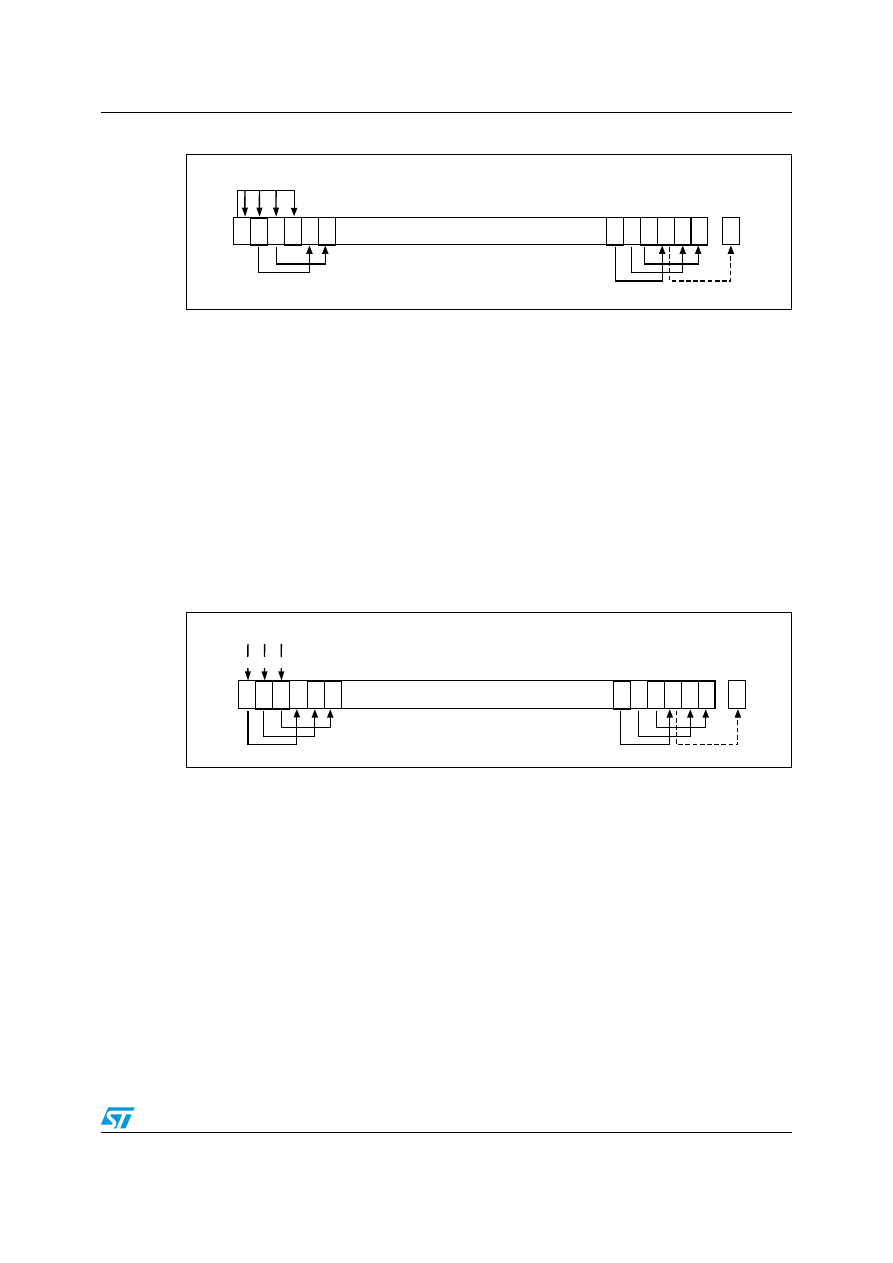
PM0056
The Cortex-M3 instruction set
Doc ID 15491 Rev 3
Figure 13.
ASR#3
LSR
Logical shift right by n bits moves the left-hand 32-n bits of the register Rm, to the right by n
places, into the right-hand 32-n bits of the result. And it sets the left-hand n bits of the result
to 0 (see
You can use the LSR #n operation to divide the value in the register Rm by 2
n
, if the value is
regarded as an unsigned integer.
When the instruction is LSRS or when LSR #n is used in operand2 with the instructions
MOVS, MVNS, ANDS, ORRS, ORNS, EORS, BICS, TEQ or TST, the carry flag is updated
to the last bit shifted out, bit[n-1], of the register Rm.
Note:
1
If n is 32 or more, then all the bits in the result are cleared to 0.
2
If n is 33 or more and the carry flag is updated, it is updated to 0.
Figure 14.
LSR#3
LSL
Logical shift left by n bits moves the right-hand 32-n bits of the register Rm, to the left by n
places, into the left-hand 32-n bits of the result. And it sets the right-hand n bits of the result
to 0 (see
You can use the LSL #n operation to multiply the value in the register Rm by 2
n
, if the value
is regarded as an unsigned integer or a two’s complement signed integer. Overflow can
occur without warning.
When the instruction is LSLS or when LSL #n, with non-zero n, is used in operand2 with the
instructions MOVS, MVNS, ANDS, ORRS, ORNS, EORS, BICS, TEQ or TST, the carry flag
is updated to the last bit shifted out, bit[32-n], of the register Rm. These instructions do not
affect the carry flag when used with LSL #0.
Note:
1
If n is 32 or more, then all the bits in the result are cleared to 0.
2
If n is 33 or more and the carry flag is updated, it is updated to 0.
31
1 0
Carry
Flag
...
2
3
4
5
31
1 0
Carry
Flag
...
0
0
0
2
3
4
5
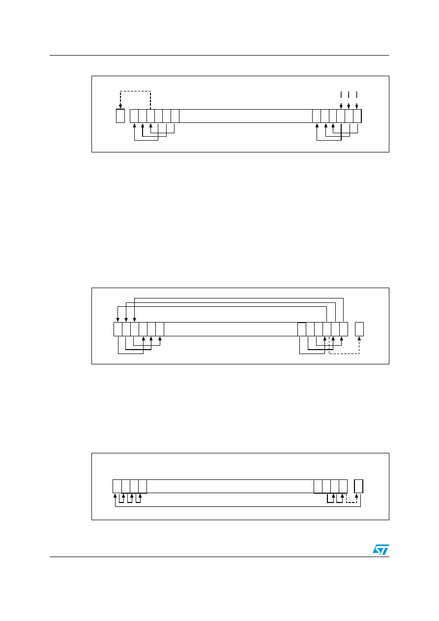
The Cortex-M3 instruction set
PM0056
Doc ID 15491 Rev 3
Figure 15.
LSL#3
ROR
Rotate right by n bits moves the left-hand 32-n bits of the register Rm, to the right by n places,
into the right-hand 32-n bits of the result. It also moves the right-hand n bits of the register
into the left-hand n bits of the result (see
When the instruction is RORS or when ROR #n is used in operand2 with the instructions
MOVS, MVNS, ANDS, ORRS, ORNS, EORS, BICS, TEQ or TST, the carry flag is updated
to the last bit rotation, bit[n-1], of the register Rm.
Note:
1
If n is 32, then the value of the result is same as the value in Rm, and if the carry flag is
updated, it is updated to bit[31] of Rm.
2
ROR with shift length, n, more than 32 is the same as ROR with shift length n-32.
Figure 16.
ROR #3
RRX
Rotate right with extend moves the bits of the register Rm to the right by one bit. And it
copies the carry flag into bit[31] of the result (see
).
When the instruction is RRXS or when RRX is used in operand2 with the instructions
MOVS, MVNS, ANDS, ORRS, ORNS, EORS, BICS, TEQ or TST, the carry flag is updated
to bit[0] of the register Rm.
Figure 17.
RRX #3
31
1 0
Carry
Flag
...
0
0
0
2
3
4
5
31
1 0
Carry
Flag
...
2
3
4
5
31 30
1
0
Carry
Flag
...
...

PM0056
The Cortex-M3 instruction set
Doc ID 15491 Rev 3
3.3.5 Address
alignment
An aligned access is an operation where a word-aligned address is used for a word, dual
word, or multiple word access, or where a halfword-aligned address is used for a halfword
access. Byte accesses are always aligned.
The Cortex-M3 processor supports unaligned access only for the following instructions:
●
LDR, LDRT
●
LDRH, LDRHT
●
LDRSH, LDRSHT
●
STR, STRT
●
STRH, STRHT
All other load and store instructions generate a usage fault exception if they perform an
unaligned access, and therefore their accesses must be address aligned. For more
information about usage faults see
.
Unaligned accesses are usually slower than aligned accesses. In addition, some memory
regions might not support unaligned accesses. Therefore, ARM recommends that
programmers ensure that accesses are aligned. To avoid accidental generation of unaligned
accesses, use the UNALIGN_TRP bit in the configuration and control register to trap all
unaligned accesses, see
Configuration and control register (SCB_CCR) on page 136
3.3.6 PC-relative
expressions
A PC-relative expression or label is a symbol that represents the address of an instruction or
literal data. It is represented in the instruction as the PC value plus or minus a numeric
offset. The assembler calculates the required offset from the label and the address of the
current instruction. If the offset is too big, the assembler produces an error.
●
For the B, BL, CBNZ, and CBZ instructions, the value of the PC is the address of the
current instruction plus four bytes.
●
For all other instructions that use labels, the value of the PC is the address of the
current instruction plus four bytes, with bit[1] of the result cleared to 0 to make it word-
aligned.
●
Your assembler might permit other syntaxes for PC-relative expressions, such as a
label plus or minus a number, or an expression of the form [PC, #number].

The Cortex-M3 instruction set
PM0056
Doc ID 15491 Rev 3
3.3.7 Conditional
execution
Most data processing instructions can optionally update the condition flags in the application
program status register (APSR) according to the result of the operation (see
program status register on page 18
). Some instructions update all flags, and some only
update a subset. If a flag is not updated, the original value is preserved. See the instruction
descriptions for the flags they affect.
You can execute an instruction conditionally, based on the condition flags set in another
instruction:
●
Immediately after the instruction that updated the flags
●
After any number of intervening instructions that have not updated the flags
Conditional execution is available by using conditional branches or by adding condition code
suffixes to instructions. See
Table 23: Condition code suffixes on page 59
for a list of the
suffixes to add to instructions to make them conditional instructions. The condition code
suffix enables the processor to test a condition based on the flags. If the condition test of a
conditional instruction fails, the instruction:
●
Does not execute
●
Does not write any value to its destination register
●
Does not affect any of the flags
●
Does not generate any exception
Conditional instructions, except for conditional branches, must be inside an If-then
instruction block. See
for more information and restrictions when using the IT
instruction. Depending on the vendor, the assembler might automatically insert an IT
instruction if you have conditional instructions outside the IT block.
Use the CBZ and CBNZ instructions to compare the value of a register against zero and
branch on the result.
This section describes:
●
●
Condition code suffixes on page 59
The condition flags
The APSR contains the following condition flags:
●
N: Set to 1 when the result of the operation is negative, otherwise cleared to 0
●
Z: Set to 1 when the result of the operation is zero, otherwise cleared to 0
●
C: Set to 1 when the operation results in a carry, otherwise cleared to 0.
●
V: Set to 1 when the operation causes an overflow, otherwise cleared to 0.
For more information about the APSR see
Program status register on page 17
.
A carry occurs:
●
If the result of an addition is greater than or equal to 2
32
●
If the result of a subtraction is positive or zero
●
As the result of an inline barrel shifter operation in a move or logical instruction
Overflow occurs if the result of an add, subtract, or compare is greater than or equal to 2
31
,
or less than -2
31
.

PM0056
The Cortex-M3 instruction set
Doc ID 15491 Rev 3
Most instructions update the status flags only if the S suffix is specified. See the instruction
descriptions for more information.
Condition code suffixes
The instructions that can be conditional have an optional condition code, shown in syntax
descriptions as {cond}. Conditional execution requires a preceding IT instruction. An
instruction with a condition code is only executed if the condition code flags in the APSR
meet the specified condition.
shows the condition codes to use.
You can use conditional execution with the IT instruction to reduce the number of branch
instructions in code.
also shows the relationship between condition code suffixes and the N, Z, C, and V
flags.
Specific example 1: Absolute value
shows the use of a conditional instruction to find the
absolute value of a number. R0 = ABS(R1).
Specific example 1: Absolute value
MOVSR0, R1; R0 = R1, setting flags
IT MI; IT instruction for the negative condition
RSBMIR0, R1, #0; If negative, R0 = -R1
Table 23.
Condition code suffixes
Suffix
Flags
Meaning
EQ
Z = 1
Equal
NE
Z = 0
Not equal
CS or HS
C = 1
Higher or same, unsigned
≥
CC or LO
C = 0
Lower, unsigned <
MI
N = 1
Negative
PL
N = 0
Positive or zero
VS
V = 1
Overflow
VC
V = 0
No overflow
HI
C = 1 and Z = 0
Higher, unsigned >
LS
C = 0 or Z = 1
Lower or same, unsigned
≤
GE
N = V
Greater than or equal, signed
≥
LT
N
! = V
Less than, signed <
GT
Z = 0 and N = V
Greater than, signed >
LE
Z = 1 and N
! = V
Less than or equal, signed
≤
AL
Can have any value
Always. This is the default when no suffix is specified.

The Cortex-M3 instruction set
PM0056
Doc ID 15491 Rev 3
Specific example 2: Compare and update value
shows the use of conditional instructions to
update the value of R4 if the signed value R0 and R2 are greater than R1 and R3 respectively.
Specific example 2: Compare and update value
CMP R0, R1 ; compare R0 and R1, setting flags
ITT GT ; IT instruction for the two GT conditions
CMPGT R2, R3; if 'greater than', compare R2 and R3, setting flags
MOVGT R4, R5 ; if still 'greater than', do R4 = R5
3.3.8 Instruction
width
selection
There are many instructions that can generate either a 16-bit encoding or a 32-bit encoding
depending on the operands and destination register specified. For some of these
instructions, you can force a specific instruction size by using an instruction width suffix.
The .W suffix forces a 32-bit instruction encoding. The .N suffix forces a 16-bit instruction
encoding.
If you specify an instruction width suffix and the assembler cannot generate an instruction
encoding of the requested width, it generates an error.
In some cases it might be necessary to specify the .W suffix, for example if the operand is
the label of an instruction or literal data, as in the case of branch instructions. This is
because the assembler might not automatically generate the right size encoding.
To use an instruction width suffix, place it immediately after the instruction mnemonic and
condition code, if any.
Specific example 3: Instruction width selection
the instruction width suffix.
Specific example 3: Instruction width selection
BCS.W label; creates a 32-bit instruction even for a short branch
ADDS.W R0, R0, R1; creates a 32-bit instruction even though the same
; operation can be done by a 16-bit instruction

PM0056
The Cortex-M3 instruction set
Doc ID 15491 Rev 3
3.4
Memory access instructions
shows the memory access instructions:
3.4.1 ADR
Load PC-relative address.
Syntax
ADR{cond} Rd, label
where:
●
‘cond’ is an optional condition code (see
Conditional execution on page 58
)
●
‘Rd’ is the destination register
●
‘label’ is a PC-relative expression (see
PC-relative expressions on page 57
Operation
ADR determines the address by adding an immediate value to the PC. It writes the result to
the destination register.
ADR produces position-independent code, because the address is PC-relative.
If you use ADR to generate a target address for a BX or BLX instruction, you must ensure
that bit[0] of the address you generate is set to1 for correct execution.
Values of label must be within the range -4095 to 4095 from the address in the PC.
Table 24.
Memory access instructions
Mnemonic
Brief description
See
ADR
Load PC-relative address
CLREX
Clear exclusive
LDM{mode}
Load multiple registers
LDR{type}
Load register using immediate offset
LDR and STR, immediate offset on page 62
LDR{type}
Load register using register offset
LDR and STR, register offset on page 64
LDR{type}T
Load register with unprivileged access
LDR and STR, unprivileged on page 65
LDR
Load register using PC-relative address
LDREX{type} Load register exclusive
POP
Pop registers from stack
PUSH
Push registers onto stack
STM{mode}
Store multiple registers
STR{type}
Store register using immediate offset
LDR and STR, immediate offset on page 62
STR{type}
Store register using register offset
LDR and STR, register offset on page 64
STR{type}T
Store register with unprivileged access
LDR and STR, unprivileged on page 65
STREX{type} Store register exclusive

The Cortex-M3 instruction set
PM0056
Doc ID 15491 Rev 3
Note:
You might have to use the .W suffix to get the maximum offset range or to generate
addresses that are not word-aligned (see
Instruction width selection on page 60
Restrictions
Rd must be neither SP nor PC.
Condition flags
This instruction does not change the flags.
Examples
ADR R1, TextMessage; write address value of a location labelled as
; TextMessage to R1
3.4.2
LDR and STR, immediate offset
Load and store with immediate offset, pre-indexed immediate offset, or post-indexed
immediate offset.
Syntax
op{type}{cond} Rt, [Rn {, #offset}]; immediate offset
op{type}{cond} Rt, [Rn, #offset]!; pre-indexed
op{type}{cond} Rt, [Rn], #offset; post-indexed
opD{cond} Rt, Rt2, [Rn {, #offset}]; immediate offset, two words
opD{cond} Rt, Rt2, [Rn, #offset]!; pre-indexed, two words
opD{cond} Rt, Rt2, [Rn], #offset; post-indexed, two words
where:
●
‘op’ is either LDR (load register) or STR (store register)
●
‘type’ is one of the following:
B: Unsigned byte, zero extends to 32 bits on loads
SB: Signed byte, sign extends to 32 bits (LDR only)
H: Unsigned halfword, zero extends to 32 bits on loads
SH: Signed halfword, sign extends to 32 bits (LDR only)
—: Omit, for word
●
‘cond’ is an optional condition code (see
Conditional execution on page 58
)
●
‘Rt’ is the register to load or store
●
‘Rn’ is the register on which the memory address is based
●
‘offset’ is an offset from Rn. If offset is omitted, the address is the contents of Rn
●
‘Rt2’ is the additional register to load or store for two-word operations

PM0056
The Cortex-M3 instruction set
Doc ID 15491 Rev 3
Operation
LDR instructions load one or two registers with a value from memory. STR instructions store
one or two register values to memory.
Load and store instructions with immediate offset can use the following addressing modes:
●
Offset addressing
The offset value is added to or subtracted from the address obtained from the register
Rn. The result is used as the address for the memory access. The register Rn is
unaltered. The assembly language syntax for this mode is: [Rn, #offset].
●
Pre-indexed addressing
The offset value is added to or subtracted from the address obtained from the register
Rn. The result is used as the address for the memory access and written back into the
register Rn. The assembly language syntax for this mode is: [Rn, #offset]!
●
Post-indexed addressing
The address obtained from the register Rn is used as the address for the memory
access. The offset value is added to or subtracted from the address, and written back
into the register Rn. The assembly language syntax for this mode is: [Rn], #offset.
The value to load or store can be a byte, halfword, word, or two words. Bytes and halfwords
can either be signed or unsigned (see
).
shows the range of offsets for immediate, pre-indexed and post-indexed forms.
Restrictions
●
For load instructions
–
Rt can be SP or PC for word loads only
–
Rt must be different from Rt2 for two-word loads
–
Rn must be different from Rt and Rt2 in the pre-indexed or post-indexed forms
●
When Rt is PC in a word load instruction
–
bit[0] of the loaded value must be 1 for correct execution
–
A branch occurs to the address created by changing bit[0] of the loaded value to 0
–
If the instruction is conditional, it must be the last instruction in the IT block
●
For store instructions
–
Rt can be SP for word stores only
–
Rt must not be PC
–
Rn must not be PC
–
Rn must be different from Rt and Rt2 in the pre-indexed or post-indexed forms
Table 25.
Immediate, pre-indexed and post-indexed offset ranges
Instruction type
Immediate offset
Pre-indexed
Post-indexed
Word, halfword, signed
halfword, byte, or signed byte
-255 to 4095
-255 to 255
-255 to 255
Two words
Multiple of 4 in the
range -1020 to 1020
Multiple of 4 in the
range -1020 to 1020
Multiple of 4 in the
range -1020 to 1020

The Cortex-M3 instruction set
PM0056
Doc ID 15491 Rev 3
Condition flags
These instructions do not change the flags.
Examples
LDRR8, [R10]; loads R8 from the address in R10.
LDRNER2, [R5, #960]!; loads (conditionally) R2 from a word
; 960 bytes above the address in R5, and
; increments R5 by 960.
STRR2, [R9,#const-struc]; const-struc is an expression evaluating
; to a constant in the range 0-4095.
STRHR3, [R4], #4; Store R3 as halfword data into address in
; R4, then increment R4 by 4
LDRD R8, R9, [R3, #0x20]; Load R8 from a word 32 bytes above the
; address in R3, and load R9 from a word 36
; bytes above the address in R3
STRDR0, R1, [R8], #-16; Store R0 to address in R8, and store R1 to
; a word 4 bytes above the address in R8,
; and then decrement R8 by 16.
3.4.3
LDR and STR, register offset
Load and store with register offset.
Syntax
op{type}{cond} Rt, [Rn, Rm {, LSL #n}]
where:
●
‘op’ is either LDR (load register) or STR (store register)
●
‘type’ is one of the following:
B: Unsigned byte, zero extends to 32 bits on loads
SB: Signed byte, sign extends to 32 bits (LDR only)
H: Unsigned halfword, zero extends to 32 bits on loads
SH: Signed halfword, sign extends to 32 bits (LDR only)
—: Omit, for word
●
‘cond’ is an optional condition code (see
Conditional execution on page 58
)
●
‘Rt’ is the register to load or store
●
‘Rn’ is the register on which the memory address is based
●
‘Rm’ is a register containing a value to be used as the offset
●
‘LSL #n’ is an optional shift, with n in the range 0 to 3
Operation
LDR instructions load a register with a value from memory. STR instructions store a register
value into memory.
The memory address to load from or store to is at an offset from the register Rn. The offset
is specified by the register Rm and can be shifted left by up to 3 bits using LSL.
The value to load or store can be a byte, halfword, or word. For load instructions, bytes and
halfwords can either be signed or unsigned (see
).

PM0056
The Cortex-M3 instruction set
Doc ID 15491 Rev 3
Restrictions
In these instructions:
●
Rn must not be PC
●
Rm must be neither SP nor PC
●
Rt can be SP only for word loads and word stores
●
Rt can be PC only for word loads
When Rt is PC in a word load instruction:
●
bit[0] of the loaded value must be 1 for correct execution, and a branch occurs to this
halfword-aligned address
●
If the instruction is conditional, it must be the last instruction in the IT block.
Condition flags
These instructions do not change the flags.
Examples
STRR0, [R5, R1]; store value of R0 into an address equal to
; sum of R5 and R1
LDRSBR0, [R5, R1, LSL #1]; read byte value from an address equal to
; sum of R5 and two times R1, sign extended it
; to a word value and put it in R0
STRR0, [R1, R2, LSL #2]; stores R0 to an address equal to sum of R1
; and four times R2
3.4.4
LDR and STR, unprivileged
Load and store with unprivileged access.
Syntax
op{type}T{cond} Rt, [Rn {, #offset}]; immediate offset
where:
●
‘op’ is either LDR (load register) or STR (store register)
●
‘type’ is one of the following:
B: Unsigned byte, zero extends to 32 bits on loads
SB: Signed byte, sign extends to 32 bits (LDR only)
H: Unsigned halfword, zero extends to 32 bits on loads
SH: Signed halfword, sign extends to 32 bits (LDR only)
—: Omit, for word
●
‘cond’ is an optional condition code (see
Conditional execution on page 58
)
●
‘Rt’ is the register to load or store
●
‘Rn’ is the register on which the memory address is based
●
‘offset’ is an offset from Rn and can be 0 to 255. If offset is omitted, the address is the
value in Rn.

The Cortex-M3 instruction set
PM0056
Doc ID 15491 Rev 3
Operation
These load and store instructions perform the same function as the memory access
instructions with immediate offset (see
LDR and STR, immediate offset on page 62
). The
difference is that these instructions have only unprivileged access even when used in
privileged software.
When used in unprivileged software, these instructions behave in exactly the same way as
normal memory access instructions with immediate offset.
Restrictions
In these instructions:
●
Rn must not be PC
●
Rt must be neither SP nor PC.
Condition flags
These instructions do not change the flags.
Examples
STRBTEQR4, [R7]; conditionally store least significant byte in
; R4 to an address in R7, with unprivileged access
LDRHTR2, [R2, #8]; load halfword value from an address equal to
; sum of R2 and 8 into R2, with unprivileged access
3.4.5 LDR,
PC-relative
Load register from memory.
Syntax
LDR{type}{cond} Rt, label
LDRD{cond} Rt, Rt2, label; load two words
where:
●
‘type’ is one of the following:
B: Unsigned byte, zero extends to 32 bits
SB: Signed byte, sign extends to 32 bits
H: Unsigned halfword, sign extends to 32 bits
SH: Signed halfword, sign extends to 32 bits
—: Omit, for word
●
‘cond’ is an optional condition code (see
Conditional execution on page 58
)
●
‘Rt’ is the register to load or store
●
‘Rt2’ is the second register to load or store
●
‘label’ is a PC-relative expression (see
PM0056
The Cortex-M3 instruction set
Doc ID 15491 Rev 3
Operation
LDR loads a register with a value from a PC-relative memory address. The memory address
is specified by a label or by an offset from the PC.
The value to load or store can be a byte, halfword, or word. For load instructions, bytes and
halfwords can either be signed or unsigned (see
).
‘label’ must be within a limited range of the current instruction.
offsets between label and the PC.
You might have to use the .W suffix to get the maximum offset range (see
).
Restrictions
In these instructions:
●
Rt can be SP or PC only for word loads
●
Rt2 must be neither SP nor PC
●
Rt must be different from Rt2
When Rt is PC in a word load instruction:
●
bit[0] of the loaded value must be 1 for correct execution, and a branch occurs to this
halfword-aligned address
●
If the instruction is conditional, it must be the last instruction in the IT block.
Condition flags
These instructions do not change the flags.
Examples
LDRR0, LookUpTable; load R0 with a word of data from an address
; labelled as LookUpTable
LDRSBR7, localdata; load a byte value from an address labelled
; as localdata, sign extend it to a word
; value, and put it in R7
Table 26.
label-PC offset ranges
Instruction type
Offset range
Word, halfword, signed halfword, byte, signed byte
−4095 to 4095
Two words
−1020 to 1020

The Cortex-M3 instruction set
PM0056
Doc ID 15491 Rev 3
3.4.6
LDM and STM
Load and store multiple registers.
Syntax
op{addr_mode}{cond} Rn{!}, reglist
where:
●
‘op’ is either LDM (load multiple register) or STM (store multiple register)
●
‘addr_mode’ is any of the following:
IA: Increment address after each access (this is the default)
DB: Decrement address before each access
●
‘cond’ is an optional condition code (see
Conditional execution on page 58
)
●
‘Rn’ is the register on which the memory addresses are based
●
‘!’ is an optional writeback suffix. If ! is present, the final address that is loaded from or
stored to is written back into Rn.
●
‘reglist’ is a list of one or more registers to be loaded or stored, enclosed in braces. It
can contain register ranges. It must be comma-separated if it contains more than one
register or register range (see
).
LDM and LDMFD are synonyms for LDMIA. LDMFD refers to its use for popping data from
full descending stacks.
LDMEA is a synonym for LDMDB, and refers to its use for popping data from empty
ascending stacks.
STM and STMEA are synonyms for STMIA. STMEA refers to its use for pushing data onto
empty ascending stacks.
STMFD is s synonym for STMDB, and refers to its use for pushing data onto full descending
stacks
Operation
LDM instructions load the registers in reglist with word values from memory addresses
based on Rn.
STM instructions store the word values in the registers in reglist to memory addresses based
on Rn.
For LDM, LDMIA, LDMFD, STM, STMIA, and STMEA the memory addresses used for the
accesses are at 4-byte intervals ranging from Rn to Rn + 4 * (n-1), where n is the number of
registers in reglist. The accesses happen in order of increasing register numbers, with the
lowest numbered register using the lowest memory address and the highest number
register using the highest memory address. If the writeback suffix is specified, the value of
Rn + 4 * (n-1) is written back to Rn.
For LDMDB, LDMEA, STMDB, and STMFD the memory addresses used for the accesses
are at 4-byte intervals ranging from Rn to Rn - 4 * (n-1), where n is the number of registers in
reglist. The accesses happen in order of decreasing register numbers, with the highest
numbered register using the highest memory address and the lowest number register using
the lowest memory address. If the writeback suffix is specified, the value Rn - 4 * (n-1) is
written back to Rn.

PM0056
The Cortex-M3 instruction set
Doc ID 15491 Rev 3
The PUSH and POP instructions can be expressed in this form (see
for
details).
Restrictions
In these instructions:
●
Rn must not be PC
●
reglist must not contain SP
●
In any STM instruction, reglist must not contain PC
●
In any LDM instruction, reglist must not contain PC if it contains LR
●
reglist must not contain Rn if you specify the writeback suffix
When PC is in reglist in an LDM instruction:
●
bit[0] of the value loaded to the PC must be 1 for correct execution, and a branch
occurs to this halfword-aligned address.
●
If the instruction is conditional, it must be the last instruction in the IT block
Condition flags
These instructions do not change the flags.
Examples
LDMR8,{R0,R2,R9}; LDMIA is a synonym for LDM
STMDBR1!,{R3-R6,R11,R12}
Incorrect examples
STMR5!,{R5,R4,R9}; value stored for R5 is unpredictable
LDMR2, {}; there must be at least one register in the list
3.4.7
PUSH and POP
Push registers onto, and pop registers off a full-descending stack.
Syntax
PUSH{cond} reglist
POP{cond} reglist
where:
●
‘cond’ is an optional condition code (see
Conditional execution on page 58
)
●
‘reglist’ is a non-empty list of registers, enclosed in braces. It can contain register
ranges. It must be comma-separated if it contains more than one register or register
range (see
PUSH and POP are synonyms for STMDB and LDM (or LDMIA) with the memory
addresses for the access based on SP, and with the final address for the access written
back to the SP. PUSH and POP are the preferred mnemonics in these cases.

The Cortex-M3 instruction set
PM0056
Doc ID 15491 Rev 3
Operation
PUSH stores registers on the stack in order of decreasing register numbers, with the highest
numbered register using the highest memory address and the lowest numbered register
using the lowest memory address.
POP loads registers from the stack in order of increasing register numbers, with the lowest
numbered register using the lowest memory address and the highest numbered register
using the highest memory address.
See
for more information.
Restrictions
In these instructions:
●
‘reglist’ must not contain SP
●
For the PUSH instruction, reglist must not contain PC
●
For the POP instruction, reglist must not contain PC if it contains LR
When PC is in reglist in a POP instruction:
●
bit[0] of the value loaded to the PC must be 1 for correct execution, and a branch
occurs to this halfword-aligned address.
●
If the instruction is conditional, it must be the last instruction in the IT block.
Condition flags
These instructions do not change the flags.
Examples
PUSH{R0,R4-R7}
PUSH{R2,LR}
POP{R0,R10,PC}

PM0056
The Cortex-M3 instruction set
Doc ID 15491 Rev 3
3.4.8
LDREX and STREX
Load and store register exclusive.
Syntax
LDREX{cond} Rt, [Rn {, #offset}]
STREX{cond} Rd, Rt, [Rn {, #offset}]
LDREXB{cond} Rt, [Rn]
STREXB{cond} Rd, Rt, [Rn]
LDREXH{cond} Rt, [Rn]
STREXH{cond} Rd, Rt, [Rn]
where:
●
‘cond’ is an optional condition code (see
Conditional execution on page 58
)
●
‘Rd’ is the destination register for the returned status
●
‘Rt’ is the register to load or store
●
‘Rn’ is the register on which the memory address is based
●
‘offset’ is an optional offset applied to the value in Rn. If offset is omitted, the address is
the value in Rn.
Operation
LDREX, LDREXB, and LDREXH load a word, byte, and halfword respectively from a
memory address.
STREX, STREXB, and STREXH attempt to store a word, byte, and halfword respectively to
a memory address. The address used in any store-exclusive instruction must be the same
as the address in the most recently executed load-exclusive instruction. The value stored by
the Store-exclusive instruction must also have the same data size as the value loaded by the
preceding load-exclusive instruction. This means software must always use a load-exclusive
instruction and a matching store-exclusive instruction to perform a synchronization
operation, see
Synchronization primitives on page 32
.
If a store-exclusive instruction performs the store, it writes 0 to its destination register. If it
does not perform the store, it writes 1 to its destination register. If the store-exclusive
instruction writes 0 to the destination register, it is guaranteed that no other process in the
system has accessed the memory location between the load-exclusive and store-exclusive
instructions.
For reasons of performance, keep the number of instructions between corresponding load-
exclusive and store-exclusive instruction to a minimum.
Note:
The result of executing a store-exclusive instruction to an address that is different from that
used in the preceding load-exclusive instruction is unpredictable.

The Cortex-M3 instruction set
PM0056
Doc ID 15491 Rev 3
Restrictions
In these instructions:
●
Do not use PC
●
Do not use SP for Rd and Rt
●
For STREX, Rd must be different from both Rt and Rn
●
The value of offset must be a multiple of four in the range 0-1020
Condition flags
These instructions do not change the flags.
Examples
MOVR1, #0x1; initialize the ‘lock taken’ value try
LDREXR0, [LockAddr]; load the lock value
CMPR0, #0; is the lock free?
ITTEQ; IT instruction for STREXEQ and CMPEQ
STREXEQR0, R1, [LockAddr]; try and claim the lock
CMPEQR0, #0; did this succeed?
BNEtry; no – try again
; yes – we have the lock
3.4.9 CLREX
Clear exclusive.
Syntax
CLREX{cond}
where:
‘cond’ is an optional condition code (see
Conditional execution on page 58
Operation
Use CLREX to make the next STREX, STREXB, or STREXH instruction write 1 to its destination
register and fail to perform the store. It is useful in exception handler code to force the failure
of the store exclusive if the exception occurs between a load exclusive instruction and the
matching store exclusive instruction in a synchronization operation.
See
Synchronization primitives on page 32
Condition flags
These instructions do not change the flags.
Examples
CLREX

PM0056
The Cortex-M3 instruction set
Doc ID 15491 Rev 3
3.5 General
data
processing instructions
shows the data processing instructions.
Table 27.
Data processing instructions
Mnemonic
Brief description
See
ADC
Add with carry
ADD, ADC, SUB, SBC, and RSB on page 74
ADD
Add
ADD, ADC, SUB, SBC, and RSB on page 74
ADDW
Add
ADD, ADC, SUB, SBC, and RSB on page 74
AND
Logical AND
AND, ORR, EOR, BIC, and ORN on page 76
ASR
Arithmetic shift right
ASR, LSL, LSR, ROR, and RRX on page 77
BIC
Bit clear
AND, ORR, EOR, BIC, and ORN on page 76
CLZ
Count leading zeros
CMN
Compare negative
CMP
Compare
EOR
Exclusive OR
AND, ORR, EOR, BIC, and ORN on page 76
LSL
Logical shift left
ASR, LSL, LSR, ROR, and RRX on page 77
LSR
Logical shift right
ASR, LSL, LSR, ROR, and RRX on page 77
MOV
Move
MOVT
Move top
MOVW
Move 16-bit constant
MVN
Move NOT
ORN
Logical OR NOT
AND, ORR, EOR, BIC, and ORN on page 76
ORR
Logical OR
AND, ORR, EOR, BIC, and ORN on page 76
RBIT
Reverse bits
REV, REV16, REVSH, and RBIT on page 82
REV
Reverse byte order in a word
REV, REV16, REVSH, and RBIT on page 82
REV16
Reverse byte order in each halfword
REV, REV16, REVSH, and RBIT on page 82
REVSH
Reverse byte order in bottom halfword
and sign extend
REV, REV16, REVSH, and RBIT on page 82
ROR
Rotate right
ASR, LSL, LSR, ROR, and RRX on page 77
RRX
Rotate right with extend
ASR, LSL, LSR, ROR, and RRX on page 77
RSB
Reverse subtract
ADD, ADC, SUB, SBC, and RSB on page 74
SBC
Subtract with carry
ADD, ADC, SUB, SBC, and RSB on page 74
SUB
Subtract
ADD, ADC, SUB, SBC, and RSB on page 74
SUBW
Subtract
ADD, ADC, SUB, SBC, and RSB on page 74
TEQ
Test equivalence
TST
Test

The Cortex-M3 instruction set
PM0056
Doc ID 15491 Rev 3
3.5.1
ADD, ADC, SUB, SBC, and RSB
Add, add with carry, subtract, subtract with carry, and reverse subtract.
Syntax
op{S}{cond} {Rd,} Rn, Operand2
op{cond} {Rd,} Rn, #imm12; ADD and SUB only
where:
●
‘op’ is one of:
ADD: Add
ADC: Add with carry
SUB: Subtract
SBC: Subtract with carry
RSB: Reverse subtract
●
‘S’ is an optional suffix. If S is specified, the condition code flags are updated on the
result of the operation (see
Conditional execution on page 58
●
‘cond’ is an optional condition code (see
Conditional execution on page 58
)
●
‘Rd’ is the destination register. If Rd is omitted, the destination register is Rn
●
‘Rn’ is the register holding the first operand
●
‘Operand2’ is a flexible second operand (see
Flexible second operand on page 53
for
details of the options).
●
‘imm12’ is any value in the range 0—4095
Operation
The ADD instruction adds the value of operand2 or imm12 to the value in Rn.
The ADC instruction adds the values in Rn and operand2, together with the carry flag.
The SUB instruction subtracts the value of operand2 or imm12 from the value in Rn.
The SBC instruction subtracts the value of operand2 from the value in Rn. If the carry flag is
clear, the result is reduced by one.
The RSB instruction subtracts the value in Rn from the value of operand2. This is useful
because of the wide range of options for operand2.
Use ADC and SBC to synthesize multiword arithmetic (see
).
ADDW is equivalent to the ADD syntax that uses the imm12 operand. SUBW is equivalent
to the SUB syntax that uses the imm12 operand.

PM0056
The Cortex-M3 instruction set
Doc ID 15491 Rev 3
Restrictions
In these instructions:
●
Operand2 must be neither SP nor PC
●
Rd can be SP only in ADD and SUB, and only with the following additional restrictions:
–
Rn must also be SP
–
Any shift in operand2 must be limited to a maximum of three bits using LSL
●
Rn can be SP only in ADD and SUB
●
Rd can be PC only in the ADD{cond} PC, PC, Rm instruction where:
–
You must not specify the S suffix
–
Rm must be neither PC nor SP
–
If the instruction is conditional, it must be the last instruction in the IT block
●
With the exception of the ADD{cond} PC, PC, Rm instruction, Rn can be PC only in
ADD and SUB, and only with the following additional restrictions:
–
You must not specify the S suffix
–
The second operand must be a constant in the range 0 to 4095
Note:
1
When using the PC for an addition or a subtraction, bits[1:0] of the PC are rounded to b00
before performing the calculation, making the base address for the calculation word-aligned.
2
If you want to generate the address of an instruction, you have to adjust the constant based
on the value of the PC. ARM recommends that you use the ADR instruction instead of ADD or
SUB with Rn equal to the PC, because your assembler automatically calculates the correct
constant for the ADR instruction.
When Rd is PC in the ADD{cond} PC, PC, Rm instruction:
●
bit[0] of the value written to the PC is ignored
●
A branch occurs to the address created by forcing bit[0] of that value to 0
Condition flags
If S is specified, these instructions update the N, Z, C and V flags according to the result.
Examples
ADDR2, R1, R3
SUBSR8, R6, #240; sets the flags on the result
RSBR4, R4, #1280; subtracts contents of R4 from 1280
ADCHIR11, R0, R3; only executed if C flag set and Z
; flag clear
Multiword arithmetic examples
Specific example 4: 64-bit addition
shows two instructions that add a 64-bit integer
contained in R2 and R3 to another 64-bit integer contained in R0 and R1, and place the
result in R4 and R5.
Specific example 4: 64-bit addition
ADDSR4, R0, R2; add the least significant words
ADCR5, R1, R3; add the most significant words with carry

The Cortex-M3 instruction set
PM0056
Doc ID 15491 Rev 3
Multiword values do not have to use consecutive registers.
shows instructions that subtract a 96-bit integer contained in R9, R1, and R11
from another contained in R6, R2, and R8. The example stores the result in R6, R9, and R2.
Specific example 5: 96-bit subtraction
SUBSR6, R6, R9; subtract the least significant words
SBCSR9, R2, R1; subtract the middle words with carry
SBCR2, R8, R11; subtract the most significant words with carry
3.5.2
AND, ORR, EOR, BIC, and ORN
Logical AND, OR, exclusive OR, bit clear, and OR NOT.
Syntax
op{S}{cond} {Rd,} Rn, Operand2
where:
●
‘op’ is one of:
AND: Logical AND
ORR: Logical OR or bit set
EOR: Logical exclusive OR
BIC: Logical AND NOT or bit clear
ORN: Logical OR NOT
●
‘S’ is an optional suffix. If S is specified, the condition code flags are updated on the
result of the operation (see
Conditional execution on page 58
●
‘cond’ is an optional condition code (see
Conditional execution on page 58
)
●
‘Rd’ is the destination register
●
‘Rn’ is the register holding the first operand
●
‘Operand2’ is a flexible second operand (see
Flexible second operand on page 53
for
details of the options).
Operation
The AND, EOR, and ORR instructions perform bitwise AND, exclusive OR, and OR
operations on the values in Rn and operand2.
The BIC instruction performs an AND operation on the bits in Rn with the complements of
the corresponding bits in the value of operand2.
The ORN instruction performs an OR operation on the bits in Rn with the complements of
the corresponding bits in the value of operand2.
Restrictions
Do not use either SP or PC.

PM0056
The Cortex-M3 instruction set
Doc ID 15491 Rev 3
Condition flags
If S is specified, these instructions:
●
Update the N and Z flags according to the result
●
Can update the C flag during the calculation of operand2 (see
●
Do not affect the V flag
Examples
ANDR9, R2,#0xFF00
ORREQR2, R0, R5
ANDSR9, R8, #0x19
EORSR7, R11, #0x18181818
BICR0, R1, #0xab
ORNR7, R11, R14, ROR #4
ORNSR7, R11, R14, ASR #32
3.5.3
ASR, LSL, LSR, ROR, and RRX
Arithmetic shift right, logical shift left, logical shift right, rotate right, and rotate right with
extend.
Syntax
op{S}{cond} Rd, Rm, Rs
op{S}{cond} Rd, Rm, #n
RRX{S}{cond} Rd, Rm
where:
●
‘op’ is one of:
ASR: Arithmetic shift right
LSL: Logical shift left
LSR: Logical shift right
ROR: Rotate right
●
‘S’ is an optional suffix. If S is specified, the condition code flags are updated on the
result of the operation (see
Conditional execution on page 58
●
‘Rd’ is the destination register
●
‘Rm’ is the register holding the value to be shifted
●
‘Rs’ is the register holding the shift length to apply to the value Rm. Only the least
significant byte is used and can be in the range 0 to 255.
●
‘n’ is the shift length. The range of shift lengths depend on the instruction as follows:
ASR: Shift length from 1 to 32
LSL: Shift length from 0 to 31
LSR: Shift length from 1 to 32
ROR: Shift length from 1 to 31
Note:
MOV{S}{cond} Rd, Rm is the preferred syntax for LSL{S}{cond} Rd, Rm, #0.

The Cortex-M3 instruction set
PM0056
Doc ID 15491 Rev 3
Operation
ASR, LSL, LSR, and ROR move the bits in the register Rm to the left or right by the number
of places specified by constant n or register Rs.
RRX moves the bits in register Rm to the right by 1.
In all these instructions, the result is written to Rd, but the value in register Rm remains
unchanged. For details on what result is generated by the different instructions (see
Restrictions
Do not use either SP or PC.
Condition flags
If S is specified:
●
These instructions update the N and Z flags according to the result
●
The C flag is updated to the last bit shifted out, except when the shift length is 0 (see
).
Examples
ASRR7, R8, #9; arithmetic shift right by 9 bits
LSLSR1, R2, #3; logical shift left by 3 bits with flag update
LSRR4, R5, #6; logical shift right by 6 bits
RORR4, R5, R6; rotate right by the value in the bottom byte of R6
RRXR4, R5; rotate right with extend
3.5.4 CLZ
Count leading zeros.
Syntax
CLZ{cond} Rd, Rm
where:
●
‘cond’ is an optional condition code (see
Conditional execution on page 58
)
●
‘Rd’ is the destination register
●
‘Rm’ is the operand register
Operation
The CLZ instruction counts the number of leading zeros in the value in Rm and returns the
result in Rd. The result value is 32 if no bits are set in the source register, and zero if bit[31]
is set.
Restrictions
Do not use either SP or PC.
Condition flags
This instruction does not change the flags.

PM0056
The Cortex-M3 instruction set
Doc ID 15491 Rev 3
Examples
CLZR4,R9
CLZNER2,R3
3.5.5 CMP
and
CMN
Compare and compare negative.
Syntax
CMP{cond} Rn, Operand2
CMN{cond} Rn, Operand2
where:
●
‘cond’ is an optional condition code (see
Conditional execution on page 58
)
●
‘Rn’ is the register holding the first operand
●
‘Operand2’ is a flexible second operand (see
Flexible second operand on page 53
) for
details of the options.
Operation
These instructions compare the value in a register with operand2. They update the condition
flags on the result, but do not write the result to a register.
The CMP instruction subtracts the value of operand2 from the value in Rn. This is the same
as a SUBS instruction, except that the result is discarded.
The CMN instruction adds the value of operand2 to the value in Rn. This is the same as an
ADDS instruction, except that the result is discarded.
Restrictions
In these instructions:
•
Do not use PC
•
Operand2 must not be SP
Condition flags
These instructions update the N, Z, C and V flags according to the result.
Examples
CMPR2, R9
CMNR0, #6400
CMPGTSP, R7, LSL #2

The Cortex-M3 instruction set
PM0056
Doc ID 15491 Rev 3
3.5.6
MOV and MVN
Move and move NOT.
Syntax
MOV{S}{cond} Rd, Operand2
MOV{cond} Rd, #imm16
MVN{S}{cond} Rd, Operand2
where:
●
‘S’ is an optional suffix. If S is specified, the condition code flags are updated on the
result of the operation (see
Conditional execution on page 58
●
‘cond’ is an optional condition code (see
Conditional execution on page 58
)
●
‘Rd’ is the destination register
●
‘Operand2’ is a flexible second operand (see
Flexible second operand on page 53
) for
details of the options.
●
‘imm16’ is any value in the range 0—65535
Operation
The MOV instruction copies the value of operand2 into Rd.
When operand2 in a MOV instruction is a register with a shift other than LSL #0, the
preferred syntax is the corresponding shift instruction:
●
ASR{S}{cond} Rd, Rm, #n is the preferred syntax for MOV{S}{cond} Rd, Rm, ASR #n
●
LSL{S}{cond} Rd, Rm, #n is the preferred syntax for MOV{S}{cond} Rd, Rm, LSL #n if n
!= 0
●
LSR{S}{cond} Rd, Rm, #n is the preferred syntax for MOV{S}{cond} Rd, Rm, LSR #n
●
ROR{S}{cond} Rd, Rm, #n is the preferred syntax for MOV{S}{cond} Rd, Rm, ROR #n
●
RRX{S}{cond} Rd, Rm is the preferred syntax for MOV{S}{cond} Rd, Rm, RRX
Also, the MOV instruction permits additional forms of operand2 as synonyms for shift
instructions:
●
MOV{S}{cond} Rd, Rm, ASR Rs is a synonym for ASR{S}{cond} Rd, Rm, Rs
●
MOV{S}{cond} Rd, Rm, LSL Rs is a synonym for LSL{S}{cond} Rd, Rm, Rs
●
MOV{S}{cond} Rd, Rm, LSR Rs is a synonym for LSR{S}{cond} Rd, Rm, Rs
●
MOV{S}{cond} Rd, Rm, ROR Rs is a synonym for ROR{S}{cond} Rd, Rm, Rs
See
ASR, LSL, LSR, ROR, and RRX on page 77
The MVN instruction takes the value of operand2, performs a bitwise logical NOT operation on
the value, and places the result into Rd.
Note:
The MOVW instruction provides the same function as MOV, but is restricted to using the imm16
operand.

PM0056
The Cortex-M3 instruction set
Doc ID 15491 Rev 3
Restrictions
You can use SP and PC only in the MOV instruction, with the following restrictions:
●
The second operand must be a register without shift
●
You must not specify the S suffix
When Rd is PC in a MOV instruction:
●
bit[0] of the value written to the PC is ignored
●
A branch occurs to the address created by forcing bit[0] of that value to 0.
Note:
Though it is possible to use MOV as a branch instruction, ARM strongly recommends the use
of a BX or BLX instruction to branch for software portability to the ARM instruction set.
Condition flags
If S is specified, these instructions:
●
Update the N and Z flags according to the result
●
Can update the C flag during the calculation of operand2 (see
●
Do not affect the V flag
Example
MOVSR11, #0x000B; write value of 0x000B to R11, flags get updated
MOVR1, #0xFA05; write value of 0xFA05 to R1, flags are not updated
MOVSR10, R12; write value in R12 to R10, flags get updated
MOVR3, #23; write value of 23 to R3
MOVR8, SP; write value of stack pointer to R8
MVNSR2, #0xF; write value of 0xFFFFFFF0 (bitwise inverse of 0xF)
; to the R2 and update flags
3.5.7 MOVT
Move top.
Syntax
MOVT{cond} Rd, #imm16
where:
●
‘cond’ is an optional condition code (see
Conditional execution on page 58
)
●
‘Rd’ is the destination register
●
‘imm16’ is a 16-bit immediate constant
Operation
MOVT writes a 16-bit immediate value, imm16, to the top halfword, Rd[31:16], of its
destination register. The write does not affect Rd[15:0].
The MOV, MOVT instruction pair enables you to generate any 32-bit constant.
Restrictions
Rd must be neither SP nor PC.

The Cortex-M3 instruction set
PM0056
Doc ID 15491 Rev 3
Condition flags
This instruction does not change the flags.
Examples
MOVTR3, #0xF123; write 0xF123 to upper halfword of R3, lower halfword
; and APSR are unchanged
3.5.8 REV,
REV16,
REVSH, and RBIT
Reverse bytes and reverse bits.
Syntax
op{cond} Rd, Rn
where:
●
‘op’ is one of:
REV: Reverse byte order in a word
REV16: Reverse byte order in each halfword independently
REVSH: Reverse byte order in the bottom halfword, and sign extends to 32 bits
RBIT: Reverse the bit order in a 32-bit word
●
‘cond’ is an optional condition code (see
Conditional execution on page 58
)
●
‘Rd’ is the destination register
●
‘Rn’ is the register holding the operand
Operation
Use these instructions to change endianness of data:
●
REV: Converts 32-bit big-endian data into little-endian data or 32-bit little-endian data
into big-endian data.
●
REV16: Converts 16-bit big-endian data into little-endian data or 16-bit little-endian data
into big-endian data.
●
REVSH: Converts either:
–
16-bit signed big-endian data into 32-bit signed little-endian data
–
16-bit signed little-endian data into 32-bit signed big-endian data
Restrictions
Do not use either SP or PC.
Condition flags
These instructions do not change the flags.
Examples
REVR3, R7; reverse byte order of value in R7 and write it to R3
REV16 R0, R0; reverse byte order of each 16-bit halfword in R0
REVSH R0, R5 ; reverse Signed Halfword
REVHS R3, R7 ; reverse with Higher or Same condition
RBIT R7, R8 ; reverse bit order of value in R8 and write the result to R7

PM0056
The Cortex-M3 instruction set
Doc ID 15491 Rev 3
3.5.9
TST and TEQ
Test bits and test equivalence.
Syntax
TST{cond} Rn, Operand2
TEQ{cond} Rn, Operand2
where:
●
‘cond’ is an optional condition code (see
Conditional execution on page 58
)
●
‘Rn’ is the register holding the first operand
●
‘Operand2’ is a flexible second operand (see
Flexible second operand on page 53
) for
details of the options.
Operation
These instructions test the value in a register against operand2. They update the condition
flags based on the result, but do not write the result to a register.
The TST instruction performs a bitwise AND operation on the value in Rn and the value of
operand2. This is the same as the ANDS instruction, except that it discards the result.
To test whether a bit of Rn is 0 or 1, use the TST instruction with an operand2 constant that
has that bit set to 1 and all other bits cleared to 0.
The TEQ instruction performs a bitwise exclusive OR operation on the value in Rn and the
value of operand2. This is the same as the EORS instruction, except that it discards the
result.
Use the TEQ instruction to test if two values are equal without affecting the V or C flags.
TEQ is also useful for testing the sign of a value. After the comparison, the N flag is the
logical exclusive OR of the sign bits of the two operands.
Restrictions
Do not use either SP or PC.
Condition flags
These instructions:
●
Update the N and Z flags according to the result
●
Can update the C flag during the calculation of operand2 (see
●
Do not affect the V flag
Examples
TSTR0, #0x3F8; perform bitwise AND of R0 value to 0x3F8,
; APSR is updated but result is discarded
TEQEQR10, R9; conditionally test if value in R10 is equal to
; value in R9, APSR is updated but result is discarded

The Cortex-M3 instruction set
PM0056
Doc ID 15491 Rev 3
3.6
Multiply and divide instructions
shows the multiply and divide instructions.
3.6.1
MUL, MLA, and MLS
Multiply, multiply with accumulate, and multiply with subtract, using 32-bit operands, and
producing a 32-bit result.
Syntax
MUL{S}{cond} {Rd,} Rn, Rm ; Multiply
MLA{cond} Rd, Rn, Rm, Ra ; Multiply with accumulate
MLS{cond} Rd, Rn, Rm, Ra ; Multiply with subtract
where:
●
‘cond’ is an optional condition code (see
Conditional execution on page 58
)
●
‘S’ is an optional suffix. If S is specified, the condition code flags are updated on the
result of the operation (see
Conditional execution on page 58
●
‘Rd’ is the destination register. If Rd is omitted, the destination register is Rn
●
‘Rn’, ‘Rm’ are registers holding the values to be multiplied
●
‘Ra’ is a register holding the value to be added to or subtracted from
Table 28.
Multiply and divide instructions
Mnemonic
Brief description
See
MLA
Multiply with accumulate, 32-bit result
MLS
Multiply and subtract, 32-bit result
MUL
Multiply, 32-bit result
SDIV
Signed divide
SMLAL
Signed multiply with accumulate
(32x32+64), 64-bit result
UMULL, UMLAL, SMULL, and SMLAL on
page 86
SMULL
Signed multiply (32x32), 64-bit result
UMULL, UMLAL, SMULL, and SMLAL on
page 86
UDIV
Unsigned divide
UMLAL
Unsigned multiply with accumulate
(32x32+64), 64-bit result
UMULL, UMLAL, SMULL, and SMLAL on
page 86
UMULL
Unsigned multiply (32x32), 64-bit
result

PM0056
The Cortex-M3 instruction set
Doc ID 15491 Rev 3
Operation
The MUL instruction multiplies the values from Rn and Rm, and places the least significant 32
bits of the result in Rd.
The MLA instruction multiplies the values from Rn and Rm, adds the value from Ra, and
places the least significant 32 bits of the result in Rd.
The MLS instruction multiplies the values from Rn and Rm, subtracts the product from the
value from Ra, and places the least significant 32 bits of the result in Rd.
The results of these instructions do not depend on whether the operands are signed or
unsigned.
Restrictions
In these instructions, do not use SP and do not use PC.
If you use the S suffix with the MUL instruction:
●
Rd, Rn, and Rm must all be in the range R0 to R7
●
Rd must be the same as Rm
●
You must not use the cond suffix
Condition flags
If S is specified, the MUL instruction:
●
Updates the N and Z flags according to the result
●
Does not affect the C and V flags
Examples
MULR10, R2, R5; multiply, R10 = R2 x R5
MLAR10, R2, R1, R5; multiply with accumulate, R10 = (R2 x R1) + R5
MULSR0, R2, R2; multiply with flag update, R0 = R2 x R2
MULLTR2, R3, R2; conditionally multiply, R2 = R3 x R2
MLSR4, R5, R6, R7; multiply with subtract, R4 = R7 - (R5 x R6)

The Cortex-M3 instruction set
PM0056
Doc ID 15491 Rev 3
3.6.2
UMULL, UMLAL, SMULL, and SMLAL
Signed and unsigned long multiply, with optional accumulate, using 32-bit operands and
producing a 64-bit result.
Syntax
op{cond} RdLo, RdHi, Rn, Rm
where:
●
‘op’ is one of:
UMULL: Unsigned long multiply
UMLAL: Unsigned long multiply, with accumulate
SMULL: Signed long multiply
SMLAL: Signed long multiply, with accumulate
●
‘cond’ is an optional condition code (see
Conditional execution on page 58
)
●
‘RdHi, RdLo’ are the destination registers. For UMLAL and SMLAL, they also hold the
accumulating value.
●
‘Rn, Rm’ are registers holding the operands
Operation
The UMULL instruction interprets the values from Rn and Rm as unsigned integers. It
multiplies these integers and places the least significant 32 bits of the result in RdLo, and the
most significant 32 bits of the result in RdHi.
The UMLAL instruction interprets the values from Rn and Rm as unsigned integers. It
multiplies these integers, adds the 64-bit result to the 64-bit unsigned integer contained in
RdHi and RdLo, and writes the result back to RdHi and RdLo.
The SMULL instruction interprets the values from Rn and Rm as two’s complement signed
integers. It multiplies these integers and places the least significant 32 bits of the result in
RdLo, and the most significant 32 bits of the result in RdHi.
The SMLAL instruction interprets the values from Rn and Rm as two’s complement signed
integers. It multiplies these integers, adds the 64-bit result to the 64-bit signed integer
contained in RdHi and RdLo, and writes the result back to RdHi and RdLo.
Restrictions
In these instructions:
●
Do not use either SP or PC
●
RdHi and RdLo must be different registers
Condition flags
These instructions do not affect the condition code flags.
Examples
UMULLR0, R4, R5, R6; unsigned (R4,R0) = R5 x R6
SMLALR4, R5, R3, R8; signed (R5,R4) = (R5,R4) + R3 x R8

PM0056
The Cortex-M3 instruction set
Doc ID 15491 Rev 3
3.6.3
SDIV and UDIV
Signed divide and unsigned divide.
Syntax
SDIV{cond} {Rd,} Rn, Rm
UDIV{cond} {Rd,} Rn, Rm
where:
●
‘cond’ is an optional condition code (see
Conditional execution on page 58
)
●
‘Rd’ is the destination register. If Rd is omitted, the destination register is Rn
●
‘Rn,’ is the register holding the value to be divided
●
‘Rm’ is a register holding the divisor
Operation
SDIV performs a signed integer division of the value in Rn by the value in Rm.
UDIV performs an unsigned integer division of the value in Rn by the value in Rm.
For both instructions, if the value in Rn is not divisible by the value in Rm, the result is
rounded towards zero.
Restrictions
Do not use either SP or PC.
Condition flags
These instructions do not change the flags.
Examples
SDIVR0, R2, R4; signed divide, R0 = R2/R4
UDIVR8, R8, R1; unsigned divide, R8 = R8/R1

The Cortex-M3 instruction set
PM0056
Doc ID 15491 Rev 3
3.7 Saturating
instructions
This section describes the saturating instructions, SSAT and USAT.
3.7.1
SSAT and USAT
Signed saturate and unsigned saturate to any bit position, with optional shift before
saturating.
Syntax
op{cond} Rd, #n, Rm {, shift #s}
where:
●
‘op’ is one of the following:
SSAT: Saturates a signed value to a signed range
USAT: Saturates a signed value to an unsigned range
●
‘cond’ is an optional condition code (see
Conditional execution on page 58
)
●
‘Rd’ is the destination register.
●
‘n’ specifies the bit position to saturate to:
n ranges from 1 to 32 for SSAT
n ranges from 0 to 31 for USAT
●
‘Rm’ is the register containing the value to saturate
●
‘shift #s’ is an optional shift applied to Rm before saturating. It must be one of the
following:
ASR #s where s is in the range 1 to 31
LSL #s where s is in the range 0 to 31
Operation
These instructions saturate to a signed or unsigned n-bit value.
The SSAT instruction applies the specified shift, then saturates to the signed range:
-2
n–1
≤ x ≤ 2
n–1
-1.
The USAT instruction applies the specified shift, then saturates to the unsigned range:
0
≤ x ≤ 2
n
-1.
For signed n-bit saturation using SSAT, this means that:
●
If the value to be saturated is less than -2
n-1
, the result returned is -2
n-1
●
If the value to be saturated is greater than 2
n-1
-1, the result returned is 2
n-1
-1
●
otherwise, the result returned is the same as the value to be saturated.
For unsigned n-bit saturation using USAT, this means that:
●
If the value to be saturated is less than 0, the result returned is 0
●
If the value to be saturated is greater than 2
n
-1, the result returned is 2
n
-1
●
Otherwise, the result returned is the same as the value to be saturated.
If the returned result is different from the value to be saturated, it is called saturation. If
saturation occurs, the instruction sets the Q flag to 1 in the APSR. Otherwise, it leaves the Q
flag unchanged. To clear the Q flag to 0, you must use the MSR instruction, see
.
PM0056
The Cortex-M3 instruction set
Doc ID 15491 Rev 3
To read the state of the Q flag, use the MRS instruction (see
).
Restrictions
Do not use either SP or PC.
Condition flags
These instructions do not affect the condition code flags.
If saturation occurs, these instructions set the Q flag to 1.
Examples
SSATR7, #16, R7, LSL #4; logical shift left value in R7 by 4, then
; saturate it as a signed 16-bit value and
; write it back to R7
USATNER0, #7, R5; conditionally saturate value in R5 as an
; unsigned 7 bit value and write it to R0
3.8 Bitfield
instructions
shows the instructions that operate on adjacent sets of bits in registers or bitfields.
Table 29.
Packing and unpacking instructions
Mnemonic
Brief description
See
BFC
Bit field clear
BFI
Bit field insert
SBFX
Signed bit field extract
SXTB
Sign extend a byte
SXTH
Sign extend a halfword
UBFX
Unsigned bit field extract
UXTB
Zero extend a byte
UXTH
Zero extend a halfword

The Cortex-M3 instruction set
PM0056
Doc ID 15491 Rev 3
3.8.1
BFC and BFI
Bit Field Clear and Bit Field Insert.
Syntax
BFC{cond} Rd, #lsb, #width
BFI{cond} Rd, Rn, #lsb, #width
where:
●
‘cond’ is an optional condition code, see
Conditional execution on page 58
.
●
‘Rd’ is the destination register.
●
‘Rn’ is the source register.
●
‘lsb’ is the position of the least significant bit of the bitfield. lsb must be in the range 0 to
31.
●
‘width’ is the width of the bitfield and must be in the range 1 to 32-lsb.
Operation
BFC clears a bitfield in a register. It clears width bits in Rd, starting at the low bit position lsb.
Other bits in Rd are unchanged.
BFI copies a bitfield into one register from another register. It replaces width bits in Rd
starting at the low bit position lsb, with width bits from Rn starting at bit[0]. Other bits in Rd
are unchanged.
Restrictions
Do not use SP and do not use PC.
Condition flags
These instructions do not affect the flags.
Examples
BFC
R4, #8, #12
; Clear bit 8 to bit 19 (12 bits) of R4 to 0
BFI
R9, R2, #8, #12
; Replace bit 8 to bit 19 (12 bits) of R9 with
; bit 0 to bit 11 from R2
3.8.2
SBFX and UBFX
Signed Bit Field Extract and Unsigned Bit Field Extract.
Syntax
SBFX{cond} Rd, Rn, #lsb, #width
UBFX{cond} Rd, Rn, #lsb, #width

PM0056
The Cortex-M3 instruction set
Doc ID 15491 Rev 3
where:
●
‘cond’ is an optional condition code, see
Conditional execution on page 58
.
●
‘Rd’ is the destination register.
●
‘Rn’ is the source register.
●
‘lsb’ is the position of the least significant bit of the bitfield. lsb must be in the range 0 to
31.
●
‘width’ is the width of the bitfield and must be in the range 1 to 32-lsb.
Operation
SBFX extracts a bitfield from one register, sign extends it to 32 bits, and writes the result to
the destination register.
UBFX extracts a bitfield from one register, zero extends it to 32 bits, and writes the result to
the destination register.
Restrictions
Do not use SP and do not use PC.
Condition flags
These instructions do not affect the flags.
Examples
SBFX
R0, R1, #20, #4
; Extract bit 20 to bit 23 (4 bits) from R1 and sign
; extend to 32 bits and then write the result to R0.
UBFX
R8, R11, #9, #10 ; Extract bit 9 to bit 18 (10 bits) from R11 and zero
; extend to 32 bits and then write the result to R8
3.8.3
SXT and UXT
Sign extend and Zero extend.
Syntax
SXTextend{cond} {Rd,} Rm {, ROR #n}
UXTextend{cond} {Rd}, Rm {, ROR #n}
where:
●
‘extend’ is one of:
B: Extends an 8-bit value to a 32-bit value.
H: Extends a 16-bit value to a 32-bit value.
●
‘cond’ is an optional condition code, see
Conditional execution on page 58
.
●
‘Rd’ is the destination register.
●
‘Rm’ is the register holding the value to extend.
●
ROR #n is one of:
ROR #8: Value from Rm is rotated right 8 bits.
ROR #16: Value from Rm is rotated right 16 bits.
ROR #24: Value from Rm is rotated right 24 bits.
If ROR #n is omitted, no rotation is performed.
The Cortex-M3 instruction set
PM0056
Doc ID 15491 Rev 3
Operation
These instructions do the following:
1.
Rotate the value from Rm right by 0, 8, 16 or 24 bits.
2.
Extract bits from the resulting value:
–
SXTB extracts bits[7:0] and sign extends to 32 bits.
–
UXTB extracts bits[7:0] and zero extends to 32 bits.
–
SXTH extracts bits[15:0] and sign extends to 32 bits.
–
UXTH extracts bits[15:0] and zero extends to 32 bits.
Restrictions
Do not use SP and do not use PC.
Condition flags
These instructions do not affect the flags.
Examples
SXTH
R4, R6, ROR #16
; Rotate R6 right by 16 bits, then obtain the lower
; halfword of the result and then sign extend to
; 32 bits and write the result to R4.
UXTB
R3, R10
; Extract lowest byte of the value in R10 and zero
; extend it, and write the result to R3
3.8.4
Branch and control instructions
shows the branch and control instructions:
Table 30.
Branch and control instructions
Mnemonic
Brief description
See
B
Branch
BL
Branch with Link
BLX
Branch indirect with Link
BX
Branch indirect
CBNZ
Compare and Branch if Non
Zero
CBZ
Compare and Branch if Non
Zero
IT
If-Then
TBB
Table Branch Byte
TBH
Table Branch Halfword
PM0056
The Cortex-M3 instruction set
Doc ID 15491 Rev 3
3.8.5
B, BL, BX, and BLX
Branch instructions.
Syntax
B{cond} label
BL{cond} label
BX{cond} Rm
BLX{cond} Rm
where:
●
‘B’ is branch (immediate).
●
‘BL’ is branch with link (immediate).
●
‘BX’ is branch indirect (register).
●
‘BLX’ is branch indirect with link (register).
●
‘cond’ is an optional condition code, see
Conditional execution on page 58
.
●
‘label’ is a PC-relative expression. See
PC-relative expressions on page 57
●
‘Rm’ is a register that indicates an address to branch to. Bit[0] of the value in Rm must
be 1, but the address to branch to is created by changing bit[0] to 0.
Operation
All these instructions cause a branch to label, or to the address indicated in Rm. In addition:
●
The BL and BLX instructions write the address of the next instruction to LR (the link
register, R14).
●
The BX and BLX instructions cause a UsageFault exception if bit[0] of Rm is 0.
B cond label is the only conditional instruction that can be either inside or outside an IT
block. All other branch instructions must be conditional inside an IT block, and must be
unconditional outside the IT block, see
.
shows the ranges for the various branch instructions.
You might have to use the .W suffix to get the maximum branch range. See
.
Table 31.
Branch ranges
Instruction
Branch range
B label
−16 MB to +16 MB
Bcond label (outside IT block)
−1 MB to +1 MB
Bcond label (inside IT block)
−16 MB to +16 MB
BL{cond} label
−16 MB to +16 MB
BX{cond} Rm
Any value in register
BLX{cond} Rm
Any value in register

The Cortex-M3 instruction set
PM0056
Doc ID 15491 Rev 3
Restrictions
The restrictions are:
●
Do not use PC in the BLX instruction
●
For BX and BLX, bit[0] of Rm must be 1 for correct execution but a branch occurs to the
target address created by changing bit[0] to 0
●
When any of these instructions is inside an IT block, it must be the last instruction of the
IT block.
Bcond is the only conditional instruction that is not required to be inside an IT block.
However, it has a longer branch range when it is inside an IT block.
Condition flags
These instructions do not change the flags.
Examples
B
loopA
; Branch to loopA
BLE
ng
; Conditionally branch to label ng
B.W
target ; Branch to target within 16MB range
BEQ
target ; Conditionally branch to target
BEQ.W
target ; Conditionally branch to target within 1MB
BL
funC
; Branch with link (Call) to function funC, return address
; stored in LR
BX
LR
; Return from function call
BXNE
R0
; Conditionally branch to address stored in R0
BLX
R0
; Branch with link and exchange (Call) to a address stored
; in R0
3.8.6
CBZ and CBNZ
Compare and branch on zero, compare and branch on non-zero.
Syntax
CBZ Rn, label
CBNZ Rn, label
where:
●
‘Rn’ is the register holding the operand.
●
‘label’ is the branch destination.
Operation
Use the CBZ or CBNZ instructions to avoid changing the condition code flags and to reduce
the number of instructions.
CBZ Rn, label does not change condition flags but is otherwise equivalent to:
CMP
Rn, #0
BEQ
label
CBNZ Rn, label does not change condition flags but is otherwise equivalent to:
CMP
Rn, #0
BNE
label

PM0056
The Cortex-M3 instruction set
Doc ID 15491 Rev 3
Restrictions
The restrictions are:
●
Rn must be in the range of R0 to R7
●
The branch destination must be within 4 to 130 bytes after the instruction
●
These instructions must not be used inside an IT block.
Condition flags
These instructions do not change the flags.
Examples
CBZ
R5, target ; Forward branch if R5 is zero
CBNZ
R0, target ; Forward branch if R0 is not zero
3.8.7 IT
If-Then condition instruction.
Syntax
IT{x{y{z}}} cond
where:
●
‘x’ specifies the condition switch for the second instruction in the IT block.
●
‘y’ specifies the condition switch for the third instruction in the IT block.
●
‘z’ specifies the condition switch for the fourth instruction in the IT block.
●
‘cond’ specifies the condition for the first instruction in the IT block.
The condition switch for the second, third and fourth instruction in the IT block can be either:
T: Then. Applies the condition cond to the instruction.
E: Else. Applies the inverse condition of cond to the instruction.
a)
It is possible to use AL (the always condition) for cond in an IT instruction. If this is
done, all of the instructions in the IT block must be unconditional, and each of x, y,
and z must be T or omitted but not E.
Operation
The IT instruction makes up to four following instructions conditional. The conditions can be
all the same, or some of them can be the logical inverse of the others. The conditional
instructions following the IT instruction form the IT block.
The instructions in the IT block, including any branches, must specify the condition in the
{cond} part of their syntax.
Your assembler might be able to generate the required IT instructions for conditional
instructions automatically, so that you do not need to write them yourself. See your
assembler documentation for details.
A BKPT instruction in an IT block is always executed, even if its condition fails.

The Cortex-M3 instruction set
PM0056
Doc ID 15491 Rev 3
Exceptions can be taken between an IT instruction and the corresponding IT block, or within
an IT block. Such an exception results in entry to the appropriate exception handler, with
suitable return information in LR and stacked PSR.
Instructions designed for use for exception returns can be used as normal to return from the
exception, and execution of the IT block resumes correctly. This is the only way that a PC-
modifying instruction is permitted to branch to an instruction in an IT block.
Restrictions
The following instructions are not permitted in an IT block:
●
IT
●
CBZ and CBNZ
●
CPSID and CPSIE.
Other restrictions when using an IT block are:
●
a branch or any instruction that modifies the PC must either be outside an IT block or
must be the last instruction inside the IT block. These are:
–
ADD PC, PC, Rm
–
MOV PC, Rm
–
B, BL, BX, BLX
–
any LDM, LDR, or POP instruction that writes to the PC
–
TBB and TBH
●
Do not branch to any instruction inside an IT block, except when returning from an
exception handler
●
All conditional instructions except Bcond must be inside an IT block. Bcond can be
either outside or inside an IT block but has a larger branch range if it is inside one
●
Each instruction inside the IT block must specify a condition code suffix that is either
the same or logical inverse as for the other instructions in the block.
Your assembler might place extra restrictions on the use of IT blocks, such as prohibiting the
use of assembler directives within them.
Condition flags
This instruction does not change the flags.
Example
ITTE
NE
; Next 3 instructions are conditional
ANDNE
R0, R0, R1
; ANDNE does not update condition flags
ADDSNE R2, R2, #1
; ADDSNE updates condition flags
MOVEQ
R2, R3
; Conditional move
CMP
R0, #9
; Convert R0 hex value (0 to 15) into ASCII
; ('0'-'9', 'A'-'F')
ITE
GT
; Next 2 instructions are conditional
ADDGT
R1, R0, #55
; Convert 0xA -> 'A'
ADDLE
R1, R0, #48
; Convert 0x0 -> '0'
IT
GT
; IT block with only one conditional instruction

PM0056
The Cortex-M3 instruction set
Doc ID 15491 Rev 3
ADDGT
R1, R1, #1
; Increment R1 conditionally
ITTEE
EQ
; Next 4 instructions are conditional
MOVEQ
R0, R1
; Conditional move
ADDEQ
R2, R2, #10
; Conditional add
ANDNE
R3, R3, #1
; Conditional AND
BNE.W
dloop
; Branch instruction can only be used in the last
; instruction of an IT block
IT
NE
; Next instruction is conditional
ADD
R0, R0, R1
; Syntax error: no condition code used in IT block
3.8.8
TBB and TBH
Table Branch Byte and Table Branch Halfword.
Syntax
TBB [Rn, Rm]
TBH [Rn, Rm, LSL #1]
where:
●
‘Rn’ is the register containing the address of the table of branch lengths.
If Rn is PC, then the address of the table is the address of the byte immediately
following the TBB or TBH instruction.
●
‘Rm’ is the index register. This contains an index into the table. For halfword tables, LSL
#1 doubles the value in Rm to form the right offset into the table.
Operation
These instructions cause a PC-relative forward branch using a table of single byte offsets for
TBB, or halfword offsets for TBH. Rn provides a pointer to the table, and Rm supplies an
index into the table. For TBB the branch offset is twice the unsigned value of the byte
returned from the table. and for TBH the branch offset is twice the unsigned value of the
halfword returned from the table. The branch occurs to the address at that offset from the
address of the byte immediately after the TBB or TBH instruction.
Restrictions
The restrictions are:
●
Rn must not be SP
●
Rm must not be SP and must not be PC
●
When any of these instructions is used inside an IT block, it must be the last instruction
of the IT block.
Condition flags
These instructions do not change the flags.

The Cortex-M3 instruction set
PM0056
Doc ID 15491 Rev 3
Examples
ADR.W
R0, BranchTable_Byte
TBB
[R0, R1]
; R1 is the index, R0 is the base address of the
; branch table
Case1
; an instruction sequence follows
Case2
; an instruction sequence follows
Case3
; an instruction sequence follows
BranchTable_Byte
DCB
0
; Case1 offset calculation
DCB
((Case2-Case1)/2)
; Case2 offset calculation
DCB
((Case3-Case1)/2)
; Case3 offset calculation
TBH
[PC, R1, LSL #1]
; R1 is the index, PC is used as base of the
; branch table
BranchTable_H
DCI
((CaseA - BranchTable_H)/2)
; CaseA offset calculation
DCI
((CaseB - BranchTable_H)/2)
; CaseB offset calculation
DCI
((CaseC - BranchTable_H)/2)
; CaseC offset calculation
CaseA
; an instruction sequence follows
CaseB
; an instruction sequence follows
CaseC
; an instruction sequence follows
3.9 Miscellaneous
instructions
shows the remaining Cortex-M3 instructions:
Table 32.
Miscellaneous instructions
Mnemonic
Brief description
See
BKPT
Breakpoint
CPSID
Change Processor State, Disable Interrupts
CPSIE
Change Processor State, Enable Interrupts
DMB
Data Memory Barrier
DSB
Data Synchronization Barrier
ISB
Instruction Synchronization Barrier
MRS
Move from special register to register
MSR
Move from register to special register
NOP
No Operation
SEV
Send Event
SVC
Supervisor Call

PM0056
The Cortex-M3 instruction set
Doc ID 15491 Rev 3
3.9.1 BKPT
Breakpoint.
Syntax
BKPT #imm
where:
●
‘imm’ is an expression evaluating to an integer in the range 0-255 (8-bit value).
Operation
The BKPT instruction causes the processor to enter Debug state. Debug tools can use this
to investigate system state when the instruction at a particular address is reached.
imm is ignored by the processor. If required, a debugger can use it to store additional
information about the breakpoint.
The BKPT instruction can be placed inside an IT block, but it executes unconditionally,
unaffected by the condition specified by the IT instruction.
Condition flags
This instruction does not change the flags.
Examples
BKPT 0xAB
; Breakpoint with immediate value set to 0xAB (debugger can
; extract the immediate value by locating it using the PC)
3.9.2 CPS
Change Processor State.
Syntax
CPSeffect iflags
where:
●
‘effect’ is one of:
IE: Clears the special purpose register.
ID: Sets the special purpose register.
●
‘iflags’ is a sequence of one or more flags:
i: Set or clear PRIMASK.
f: Set or clear FAULTMASK.
WFE
Wait For Event
WFI
Wait For Interrupt
Table 32.
Miscellaneous instructions (continued)
Mnemonic
Brief description
See

The Cortex-M3 instruction set
PM0056
Doc ID 15491 Rev 3
Operation
CPS changes the PRIMASK and FAULTMASK special register values. See
for more information about these registers.
Restrictions
The restrictions are:
●
Use CPS only from privileged software, it has no effect if used in unprivileged software
●
CPS cannot be conditional and so must not be used inside an IT block.
Condition flags
This instruction does not change the condition flags.
Examples
CPSID i
; Disable interrupts and configurable fault handlers (set PRIMASK)
CPSID f
; Disable interrupts and all fault handlers (set FAULTMASK)
CPSIE i
; Enable interrupts and configurable fault handlers (clear PRIMASK)
CPSIE f
; Enable interrupts and fault handlers (clear FAULTMASK)
3.9.3 DMB
Data Memory Barrier.
Syntax
DMB{cond}
where:
●
‘cond’ is an optional condition code, see
Conditional execution on page 58
.
Operation
DMB acts as a data memory barrier. It ensures that all explicit memory accesses that
appear, in program order, before the DMB instruction are completed before any explicit
memory accesses that appear, in program order, after the DMB instruction. DMB does not
affect the ordering or execution of instructions that do not access memory.
Condition flags
This instruction does not change the flags.
Examples
DMB
; Data Memory Barrier
3.9.4 DSB
Data Synchronization Barrier.
Syntax
DSB{cond}

PM0056
The Cortex-M3 instruction set
Doc ID 15491 Rev 3
101/154
where:
●
‘cond’ is an optional condition code, see
Conditional execution on page 58
.
Operation
DSB acts as a special data synchronization memory barrier. Instructions that come after the
DSB, in program order, do not execute until the DSB instruction completes. The DSB
instruction completes when all explicit memory accesses before it complete.
Condition flags
This instruction does not change the flags.
Examples
DSB ; Data Synchronisation Barrier
3.9.5 ISB
Instruction Synchronization Barrier.
Syntax
ISB{cond}
where:
●
‘cond’ is an optional condition code, see
Conditional execution on page 58
.
Operation
ISB acts as an instruction synchronization barrier. It flushes the pipeline of the processor, so
that all instructions following the ISB are fetched from cache or memory again, after the ISB
instruction has been completed.
Condition flags
This instruction does not change the flags.
Examples
ISB
; Instruction Synchronisation Barrier
3.9.6 MRS
Move the contents of a special register to a general-purpose register.
Syntax
MRS{cond} Rd, spec_reg

The Cortex-M3 instruction set
PM0056
102/154
Doc ID 15491 Rev 3
where:
●
‘cond’ is an optional condition code, see
Conditional execution on page 58
.
●
‘Rd’ is the destination register.
●
‘spec_reg’ can be any of: APSR, IPSR, EPSR, IEPSR, IAPSR, EAPSR, PSR, MSP,
PSP, PRIMASK, BASEPRI, BASEPRI_MAX, FAULTMASK, or CONTROL.
Operation
Use MRS in combination with MSR as part of a read-modify-write sequence for updating a
PSR, for example to clear the Q flag.
In process swap code, the programmers model state of the process being swapped out
must be saved, including relevant PSR contents. Similarly, the state of the process being
swapped in must also be restored. These operations use MRS in the state-saving
instruction sequence and MSR in the state-restoring instruction sequence.
BASEPRI_MAX is an alias of BASEPRI when used with the MRS instruction.
See
Restrictions
Rd must not be SP and must not be PC.
Condition flags
This instruction does not change the flags.
Examples
MRS
R0, PRIMASK ; Read PRIMASK value and write it to R0
3.9.7 MSR
Move the contents of a general-purpose register into the specified special register.
Syntax
MSR{cond} spec_reg, Rn
where:
●
‘cond’ is an optional condition code, see
Conditional execution on page 58
.
●
‘Rn’ is the source register.
●
‘spec_reg’ can be any of: APSR, IPSR, EPSR, IEPSR, IAPSR, EAPSR, PSR, MSP,
PSP, PRIMASK, BASEPRI, BASEPRI_MAX, FAULTMASK, or CONTROL.
Operation
The register access operation in MSR depends on the privilege level. Unprivileged software
can only access the APSR, see
Table 4: APSR bit definitions on page 18
. Privileged
software can access all special registers.
In unprivileged software writes to unallocated or execution state bits in the PSR are ignored.

PM0056
The Cortex-M3 instruction set
Doc ID 15491 Rev 3
103/154
When you write to BASEPRI_MAX, the instruction writes to BASEPRI only if either:
●
Rn is non-zero and the current BASEPRI value is 0
●
Rn is non-zero and less than the current BASEPRI value.
See
Restrictions
Rn must not be SP and must not be PC.
Condition flags
This instruction updates the flags explicitly based on the value in Rn.
Examples
MSR
CONTROL, R1 ; Read R1 value and write it to the CONTROL register
3.9.8 NOP
No Operation.
Syntax
NOP{cond}
where:
●
‘cond’ is an optional condition code, see
Conditional execution on page 58
.
Operation
NOP does nothing. NOP is not necessarily a time-consuming NOP. The processor might
remove it from the pipeline before it reaches the execution stage.
Use NOP for padding, for example to place the following instruction on a 64-bit boundary.
Condition flags
This instruction does not change the flags.
Examples
NOP
; No operation
3.9.9 SEV
Send Event.
Syntax
SEV{cond}
where:
●
‘cond’ is an optional condition code, see
Conditional execution on page 58
.

The Cortex-M3 instruction set
PM0056
104/154
Doc ID 15491 Rev 3
Operation
SEV is a hint instruction that causes an event to be signaled to all processors within a
multiprocessor system. It also sets the local event register to 1, see
.
Condition flags
This instruction does not change the flags.
Examples
SEV ; Send Event
3.9.10 SVC
Supervisor Call.
Syntax
SVC{cond} #imm
where:
●
‘cond’ is an optional condition code, see
Conditional execution on page 58
.
●
‘imm’ is an expression evaluating to an integer in the range 0-255 (8-bit value).
Operation
The SVC instruction causes the SVC exception.
imm is ignored by the processor. If required, it can be retrieved by the exception handler to
determine what service is being requested.
Condition flags
This instruction does not change the flags.
Examples
SVC
0x32
; Supervisor Call (SVC handler can extract the immediate value
; by locating it via the stacked PC)
3.9.11 WFE
Wait For Event.
Syntax
WFE{cond}
where:
●
‘cond’ is an optional condition code, see
Conditional execution on page 58
.
Operation
WFE is a hint instruction.

PM0056
The Cortex-M3 instruction set
Doc ID 15491 Rev 3
105/154
If the event register is 0, WFE suspends execution until one of the following events occurs:
●
An exception, unless masked by the exception mask registers or the current priority
level
●
An exception enters the Pending state, if SEVONPEND in the System Control Register
is set
●
A Debug Entry request, if Debug is enabled
●
An event signaled by a peripheral or another processor in a multiprocessor system
using the SEV instruction.
If the event register is 1, WFE clears it to 0 and returns immediately.
For more information see
.
Condition flags
This instruction does not change the flags.
Examples
WFE
; Wait for event
3.9.12 WFI
Wait for Interrupt.
Syntax
WFI{cond}
where:
●
‘cond’ is an optional condition code, see
Conditional execution on page 58
.
Operation
WFI is a hint instruction that suspends execution until one of the following events occurs:
●
An exception
●
A Debug Entry request, regardless of whether Debug is enabled.
Condition flags
This instruction does not change the flags.
Examples
WFI ; Wait for interrupt
Core peripherals
PM0056
106/154
Doc ID 15491 Rev 3
4 Core
peripherals
4.1
About the STM32 core peripherals
The address map of the Private peripheral bus (PPB) is:
In register descriptions:
●
The required privilege gives the privilege level required to access the register, as
follows:
4.2
Memory protection unit (MPU)
This section describes the Memory protection unit (MPU) which is implemented in some
STM32 microcontrollers. Refer to the corresponding device datasheet to see if the MPU is
present in the STM32 type you are using.
The MPU divides the memory map into a number of regions, and defines the location, size,
access permissions, and memory attributes of each region. It supports:
●
Independent attribute settings for each region
●
Overlapping regions
●
Export of memory attributes to the system.
The memory attributes affect the behavior of memory accesses to the region. The Cortex-
M3 MPU defines:
●
Eight separate memory regions, 0-7
●
A background region.
When memory regions overlap, a memory access is affected by the attributes of the region
with the highest number. For example, the attributes for region 7 take precedence over the
attributes of any region that overlaps region 7.
The background region has the same memory access attributes as the default memory
map, but is accessible from privileged software only.
Table 33.
STM32 core peripheral register regions
Address
Core peripheral
Description
0xE000E010-0xE000E01F
System timer
0xE000E100-0xE000E4EF
Nested vectored interrupt
controller
0xE000ED00-0xE000ED3F
System control block
0xE000ED90-0xE000ED93
Memory protection unit
(1)
1.
Software can read the MPU Type Register at 0xE000ED90 to test for the presence of a memory protection
unit (MPU).
0xE000EF00-0xE000EF03
Nested vectored interrupt
controller
Privileged
Only privileged software can access the register.
Unprivileged Both unprivileged and privileged software can access the register.

PM0056
Core peripherals
Doc ID 15491 Rev 3
107/154
The Cortex-M3 MPU memory map is unified. This means instruction accesses and data
accesses have same region settings.
If a program accesses a memory location that is prohibited by the MPU, the processor
generates a memory management fault. This causes a fault exception, and might cause
termination of the process in an OS environment.
In an OS environment, the kernel can update the MPU region setting dynamically based on
the process to be executed. Typically, an embedded OS uses the MPU for memory
protection.
Configuration of MPU regions is based on memory types, see
regions, types and attributes on page 26
.
shows the possible MPU region attributes.
4.2.1
MPU access permission attributes
This section describes the MPU access permission attributes. The access permission bits,
TEX, C, B, S, AP, and XN, of the MPU_RASR register, control access to the corresponding
memory region. If an access is made to an area of memory without the required
permissions, then the MPU generates a permission fault.
shows the encodings for the TEX, C, B, and S access permission bits.
Table 34.
Memory attributes summary
Memory type
Shareability
Other attributes
Description
Strongly- ordered
-
-
All accesses to Strongly-ordered
memory occur in program order. All
Strongly-ordered regions are
assumed to be shared.
Device
Shared
-
Memory-mapped peripherals that
several processors share.
Non-shared
-
Memory-mapped peripherals that
only a single processor uses.
Normal
Shared
Non-cacheable
Write-through
Cacheable
Write-back
Cacheable
Normal memory that is shared
between several processors.
Non-shared
Non-cacheable
Write-through
Cacheable
Write-back
Cacheable
Normal memory that only a single
processor uses.
Core peripherals
PM0056
108/154
Doc ID 15491 Rev 3
shows the cache policy for memory attribute encodings with a TEX value is in the
range 4-7.
shows the AP encodings that define the access permissions for privileged and
unprivileged software.
Table 35.
TEX, C, B, and S encoding
TEX
C
B
S
Memory type
Shareability
Other attributes
b000
0
0
x
(1)
Strongly-ordered
Shareable
-
Device
Shareable
-
1
0
0
Normal
Not shareable Outer and inner write-through. No
write allocate.
1
Shareable
1
0
Normal
Not shareable Outer and inner write-back. No write
allocate.
1
Shareable
b001
0
0
0
Normal
Not shareable
Outer and inner noncacheable.
1
Shareable
Reserved
encoding
-
1
Implementation defined
attributes.
-
1
0
Normal
Not shareable Outer and inner write-back. Write
and read allocate.
1
Shareable
b010
0
Device
Not shareable Nonshared Device.
Reserved
encoding
-
1
Reserved
encoding
-
b1BB
A
A
0
Normal
Not shareable Cached memory
(2)
, BB = outer
policy, AA = inner policy.
1
Shareable
1.
THe MPU ignores the value fo this bit.
2.
See
for the encoding of the AA and BB bits.
Table 36.
Cache policy for memory attribute encoding
Encoding, AA or BB
Corresponding cache policy
00
Non-cacheable
01
Write back, write and read allocate
10
Write through, no write allocate
11
Write back, no write allocate
Table 37.
AP encoding
AP[2:0]
Privileged
permissions
Unprivileged
permissions
Description
000
No access
No access
All accesses generate a permission fault
001
RW
No access
Access from privileged software only

PM0056
Core peripherals
Doc ID 15491 Rev 3
109/154
4.2.2 MPU
mismatch
When an access violates the MPU permissions, the processor generates a memory
management fault, see
Section 2.1.4: Exceptions and interrupts on page 23
. The MMFSR
indicates the cause of the fault. See
Section 4.4.11: Memory management fault address
register (SCB_MMFAR) on page 146
4.2.3
Updating an MPU region
To update the attributes for an MPU region, update the MPU_RNR, MPU_RBAR and
MPU_RASR registers. You can program each register separately, or use a multiple-word
write to program all of these registers. You can use the MPU_RBAR and MPU_RASR
aliases to program up to four regions simultaneously using an STM instruction.
Updating an MPU region using separate words
Simple code to configure one region:
; R1 = region number
; R2 = size/enable
; R3 = attributes
; R4 = address
LDR R0,=MPU_RNR ; 0xE000ED98, MPU region number register
STR R1, [R0, #0x0] ; Region Number
STR R4, [R0, #0x4] ; Region Base Address
STRH R2, [R0, #0x8] ; Region Size and Enable
STRH R3, [R0, #0xA] ; Region Attribute
Disable a region before writing new region settings to the MPU if you have previously
enabled the region being changed. For example:
; R1 = region number
; R2 = size/enable
; R3 = attributes
; R4 = address
LDR R0,=MPU_RNR ; 0xE000ED98, MPU region number register
STR R1, [R0, #0x0] ; Region Number
BIC R2, R2, #1 ; Disable
STRH R2, [R0, #0x8] ; Region Size and Enable
STR R4, [R0, #0x4] ; Region Base Address
STRH R3, [R0, #0xA] ; Region Attribute
ORR R2, #1 ; Enable
STRH R2, [R0, #0x8] ; Region Size and Enable
010
RW
RO
Writes by unprivileged software generate
a permission fault
011
RW
RW
Full access
100
Unpredictable
Unpredictable
Reserved
101
RO
No access
Reads by privileged software only
110
RO
RO
Read only, by privileged or unprivileged
software
111
RO
RO
Read only, by privileged or unprivileged
software
Table 37.
AP encoding (continued)
AP[2:0]
Privileged
permissions
Unprivileged
permissions
Description

Core peripherals
PM0056
110/154
Doc ID 15491 Rev 3
Software must use memory barrier instructions:
●
Before MPU setup if there might be outstanding memory transfers, such as buffered
writes, that might be affected by the change in MPU settings
●
After MPU setup if it includes memory transfers that must use the new MPU settings.
However, memory barrier instructions are not required if the MPU setup process starts by
entering an exception handler, or is followed by an exception return, because the exception
entry and exception return mechanism cause memory barrier behavior.
Software does not need any memory barrier instructions during MPU setup, because it
accesses the MPU through the PPB, which is a Strongly-Ordered memory region.
For example, if you want all of the memory access behavior to take effect immediately after
the programming sequence, use a DSB instruction and an ISB instruction. A DSB is
required after changing MPU settings, such as at the end of context switch. An ISB is
required if the code that programs the MPU region or regions is entered using a branch or
call. If the programming sequence is entered using a return from exception, or by taking an
exception, then you do not require an ISB.
Updating an MPU region using multi-word writes
You can program directly using multi-word writes, depending on how the information is
divided. Consider the following reprogramming:
; R1 = region number
; R2 = address
; R3 = size, attributes in one
LDR R0, =MPU_RNR ; 0xE000ED98, MPU region number register
STR R1, [R0, #0x0] ; Region Number
STR R2, [R0, #0x4] ; Region Base Address
STR R3, [R0, #0x8] ; Region Attribute, Size and Enable
Use an STM instruction to optimize this:
; R1 = region number
; R2 = address
; R3 = size, attributes in one
LDR R0, =MPU_RNR ; 0xE000ED98, MPU region number register
STM R0, {R1-R3} ; Region Number, address, attribute, size and enable
You can do this in two words for pre-packed information. This means that the RBAR
contains the required region number and had the VALID bit set to 1, see
address register (MPU_RBAR) on page 115
. Use this when the data is statically packed, for
example in a boot loader:
; R1 = address and region number in one
; R2 = size and attributes in one
LDR R0, =MPU_RBAR ; 0xE000ED9C, MPU Region Base register
STR R1, [R0, #0x0] ; Region base address and
; region number combined with VALID (bit 4) set to 1
STR R2, [R0, #0x4] ; Region Attribute, Size and Enable
Use an STM instruction to optimize this:
; R1 = address and region number in one
; R2 = size and attributes in one
LDR R0,=MPU_RBAR ; 0xE000ED9C, MPU Region Base register
STM R0, {R1-R2} ; Region base address, region number and VALID bit,
; and Region Attribute, Size and Enable
Subregions
Regions of 256 bytes or more are divided into eight equal-sized subregions. Set the
corresponding bit in the SRD field of the RASR to disable a subregion, see
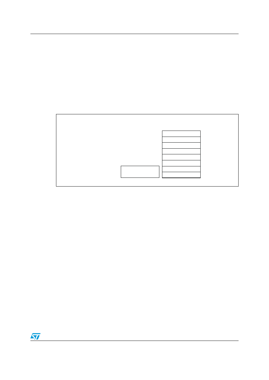
PM0056
Core peripherals
Doc ID 15491 Rev 3
111/154
MPU region attribute and size register (MPU_RASR) on page 117
. The least significant bit
of SRD controls the first subregion, and the most significant bit controls the last subregion.
Disabling a subregion means another region overlapping the disabled range matches
instead. If no other enabled region overlaps the disabled subregion the MPU issues a fault.
Regions of 32, 64, and 128 bytes do not support subregions, With regions of these sizes,
you must set the SRD field to 0x00, otherwise the MPU behavior is Unpredictable.
Example of SRD use:
Two regions with the same base address overlap. Region one is 128KB, and region two is
512KB. To ensure the attributes from region one apply to the first128KB region, set the SRD
field for region two to b00000011 to disable the first two subregions, as the figure shows.
Figure 18.
Subregion example
4.2.4 MPU
design
hints and tips
To avoid unexpected behavior, disable the interrupts before updating the attributes of a
region that the interrupt handlers might access.
Ensure software uses aligned accesses of the correct size to access MPU registers:
●
Except for the RASR, it must use aligned word accesses
●
For the RASR it can use byte or aligned halfword or word accesses.
The processor does not support unaligned accesses to MPU registers.
When setting up the MPU, and if the MPU has previously been programmed, disable
unused regions to prevent any previous region settings from affecting the new MPU setup.
Recommended MPU configuration
The STM32 microcontroller system has only a single processor, so you should program the
MPU as follows:
Region 1
Disabled subregion
Disabled subregion
Region 2, with
subregions
Base address of both regions
Offset from
base address
0
64KB
128KB
192KB
256KB
320KB
384KB
448KB
512KB
Core peripherals
PM0056
112/154
Doc ID 15491 Rev 3
In STM32 implementations, the shareability and cache policy attributes do not affect the
system behavior. However, using these settings for the MPU regions can make the
application code more portable. The values given are for typical situations.
Note:
The MPU attributes don't affect DMA data accesses to the memory/peripherals address
spaces. therefore, in order to protect the memory areas against inadvertent DMA accesses,
the MPU must control the SW/CPU access to the DMA registers.
4.2.5
MPU type register (MPU_TYPER)
Address offset: 0x00
Reset value: 0x0000 0800
Required privilege: Privileged
The MPU_TYPER register indicates whether the MPU is present, and if so, how many
regions it supports.
Table 38.
Memory region attributes for STM32
Memory region
TEX
C
B
S
Memory type and attributes
Flash memory
b000
1
0
0
Normal memory, Non-shareable,
write-through
Internal SRAM
b000
1
0
1
Normal memory, Shareable, write-
through
External SRAM
b000
1
1
1
Normal memory, Shareable, write-
back, write-allocate
Peripherals
b000
0
1
1
Device memory, Shareable
31
30
29
28
27
26
25
24
23
22
21
20
19
18
17
16
Reserved
IREGION[7:0]
r
r
r
r
r
r
r
r
15
14
13
12
11
10
9
8
7
6
5
4
3
2
1
0
DREGION[7:0]
Reserved
SEPA
RATE
r
r
r
r
r
r
r
r
Bits 31:24 Reserved, forced by hardware to 0.
Bits 23:16 IREGION[7:0]: Number of MPU instruction regions.
These bits indicates the number of supported MPU instruction regions.
Always contains 0x00. The MPU memory map is unified and is described by the DREGION
field.

PM0056
Core peripherals
Doc ID 15491 Rev 3
113/154
4.2.6
MPU control register (MPU_CR)
Address offset: 0x04
Reset value: 0x0000 0000
Required privilege: Privileged
The MPU_CR register:
●
Enables the MPU
●
Enables the default memory map background region
●
Enables use of the MPU when in the hard fault, Non-maskable Interrupt (NMI), and
FAULTMASK escalated handlers.
When ENABLE and PRIVDEFENA are both set to 1:
●
For privileged accesses, the default memory map is as described in
. Any access by privileged software that does not address
an enabled memory region behaves as defined by the default memory map.
●
Any access by unprivileged software that does not address an enabled memory region
causes a memory management fault.
XN and Strongly-ordered rules always apply to the System Control Space regardless of the
value of the ENABLE bit.
When the ENABLE bit is set to 1, at least one region of the memory map must be enabled
for the system to function unless the PRIVDEFENA bit is set to 1. If the PRIVDEFENA bit is
set to 1 and no regions are enabled, then only privileged software can operate.
When the ENABLE bit is set to 0, the system uses the default memory map. This has the
same memory attributes as if the MPU is not implemented, see
. The default memory map applies to accesses from both privileged
and unprivileged software.
When the MPU is enabled, accesses to the System Control Space and vector table are
always permitted. Other areas are accessible based on regions and whether PRIVDEFENA
is set to 1.
Unless HFNMIENA is set to 1, the MPU is not enabled when the processor is executing the
handler for an exception with priority –1 or –2. These priorities are only possible when
handling a hard fault or NMI exception, or when FAULTMASK is enabled. Setting the
HFNMIENA bit to 1 enables the MPU when operating with these two priorities.
Bits 15:8 DREGION[7:0]: Number of MPU data regions.
These bits indicates the number of supported MPU data regions.
0x08: Eight MPU regions
0x00: MPU not present
Bits 7:1 Reserved, forced by hardware to 0.
Bit 0 SEPARATE: Separate flag
This bit indicates support for unified or separate instruction and data memory maps:
0 = Unified
1 = Separate
Core peripherals
PM0056
114/154
Doc ID 15491 Rev 3
4.2.7
MPU region number register (MPU_RNR)
Address offset: 0x08
Reset value: 0x0000 0000
Required privilege: Privileged
The MPU_RNR register selects which memory region is referenced by the MPU_RBAR and
MPU_RASR registers.
31
30
29
28
27
26
25
24
23
22
21
20
19
18
17
16
Reserved
15
14
13
12
11
10
9
8
7
6
5
4
3
2
1
0
Reserved
PRIVD
EFENA
HFNMI
ENA
EN
ABLE
rw
rw
rw
Bits 31:0 Reserved, forced by hardware to 0.
Bit 2 PRIVDEFENA: Enable priviliged software access to default memory map.
0: If the MPU is enabled, disables use of the default memory map. Any memory access to a
location not covered by any enabled region causes a fault.
1: If the MPU is enabled, enables use of the default memory map as a background region for
privileged software accesses.
Note: When enabled, the background region acts as if it is region number -1. Any region that
is defined and enabled has priority over this default map.
If the MPU is disabled, the processor ignores this bit.
Bit 1 HFNMIENA: Enables the operation of MPU during hard fault, NMI, and FAULTMASK handlers.
When the MPU is enabled:
0: MPU is disabled during hard fault, NMI, and FAULTMASK handlers, regardless of the
value of the ENABLE bit
1: The MPU is enabled during hard fault, NMI, and FAULTMASK handlers.
Note: When the MPU is disabled, if this bit is set to 1 the behavior is unpredictable.
Bit 0 ENABLE: Enables the MPU
0: MPU disabled
1: MPU enabled
31
30
29
28
27
26
25
24
23
22
21
20
19
18
17
16
Reserved
15
14
13
12
11
10
9
8
7
6
5
4
3
2
1
0
Reserved
REGION[7:0]
rw
rw
rw
rw
rw
rw
rw
rw
PM0056
Core peripherals
Doc ID 15491 Rev 3
115/154
4.2.8
MPU region base address register (MPU_RBAR)
Address offset: 0x0C
Reset value: 0x0000 0000
Required privilege: Privileged
The MPU_RBAR register defines the base address of the MPU region selected by the
MPU_RNR register, and can update the value of the MPU_RNR register.
Write to the MPU_RBAR register with the VALID bit set to 1 to change the current region
number and update the MPU_RNR register.
Bits 31:8 Reserved, forced by hardware to 0.
Bits 7:0 REGION[7:0]: MPU region
These bits indicate the MPU region referenced by the MPU_RBAR and MPU_RASR registers.
The MPU supports 8 memory regions, so the permitted values of this field are 0-7.
Normally, you write the required region number to this register before accessing the
MPU_RBAR or MPU_RASR. However you can change the region number by writing to the
MPU_RBAR register with the VALID bit set to 1, see
MPU region base address register
. This write updates the value of the REGION field.
31
30
29
28
27
26
25
24
23
22
21
20
19
18
17
16
ADDR[31:N]...
15
14
13
12
11
10
9
8
7
6
5
4
3
2
1
0
....ADDR[31:N]
VALID
REGION[3:0]
rw
rw
rw
rw
rw

Core peripherals
PM0056
116/154
Doc ID 15491 Rev 3
Bits 31:N ADDR[31:N]: Region base address field
The value of N depends on the region size.
The region size, as specified by the SIZE field in the RASR, defines the value of N:
N = Log2(Region size in bytes),
If the region size is configured to 4 GB, in the MPU_RASR register, there is no valid ADDR
field. In this case, the region occupies the complete memory map, and the base address is
0x00000000.
The base address is aligned to the size of the region. For example, a 64 KB region must be
aligned on a multiple of 64 KB, for example, at 0x00010000 or 0x00020000.
Bits N-1:5 Reserved, forced by hardware to 0.
Bit 4 VALID: MPU region number valid
Write:
0: MPU_RNR register not changed, and the processor:
–
Updates the base address for the region specified in the RNR
–
Ignores the value of the REGION field
1: the processor:
–
updates the value of the RNR to the value of the REGION field
–
updates the base address for the region specified in the REGION field.
Read:
Always read as zero.
Bits 3:0 REGION[3:0]: MPU region field
For the behavior on writes, see the description of the VALID field.
On reads, returns the current region number, as specified by the MPU_RNR register.
PM0056
Core peripherals
Doc ID 15491 Rev 3
117/154
4.2.9
MPU region attribute and size register (MPU_RASR)
Address offset: 0x10
Reset value: 0x0000 0000
Required privilege: Privileged
The MPU_RASR register defines the region size and memory attributes of the MPU region
specified by the MPU_RNR, and enables that region and any subregions.
MPU_RASR is accessible using word or halfword accesses:
●
The most significant halfword holds the region attributes
●
The least significant halfword holds the region size and the region and subregion
enable bits.
31
30
29
28
27
26
25
24
23
22
21
20
19
18
17
16
Reserved
XN
Reserv
ed
AP[2:0]
Reserved
TEX[2:0]
S
C
B
rw
rw
rw
rw
rw
rw
rw
rw
rw
rw
15
14
13
12
11
10
9
8
7
6
5
4
3
2
1
0
SRD[7:0]
Reserved
SIZE
EN
ABLE
rw
rw
rw
rw
rw
rw
rw
rw
rw
rw
rw
rw
rw
rw
Bits 31:29 Reserved, forced by hardware to 0.
Bit 28 XN: Instruction access disable bit:
0: Instruction fetches enabled
1: Instruction fetches disabled.
Bit 27 Reserved, forced by hardware to 0.
Bits 26:24 AP[2:0]: Access permission
For information about access permission, see
For the description of the encoding of the AP bits refer to
.
Bits 23:22 Reserved, forced by hardware to 0.
Bits 21:19 TEX[2:0]: memory attribute
For the description of the encoding of the TEX bits refer to
Bit 18 S: Shareable memory attribute
For the description of the encoding of the S bits refer to
Bit 17 C: memory attribute
Bit 16 B: memory attribute
Bits 15:8 SRD: Subregion disable bits.
For each bit in this field:
0: corresponding sub-region is enabled
1: corresponding sub-region is disabled
for more information.
Region sizes of 128 bytes and less do not support subregions. When writing the attributes for
such a region, write the SRD field as 0x00.
Core peripherals
PM0056
118/154
Doc ID 15491 Rev 3
SIZE field values
The SIZE field defines the size of the MPU memory region specified by the MPU_RNR
regsiter as follows:
(Region size in bytes) = 2(SIZE+1)
The smallest permitted region size is 32B, corresponding to a SIZE value of 4. Table 4-45
gives example SIZE values, with the corresponding region size and value of N in the RBAR.
Bits 7:6 Reserved, forced by hardware to 0.
Bits 5:1 SIZE: Size of the MPU protection region.
The minimum permitted value is 3 (b00010), see
for more information.
Bit 0 ENABLE: Region enable bit.
Table 39.
Example SIZE field values
SIZE value
Region size
Value of N
(1)
1.
In the MPU_RBAR register see
Note
b00100 (4)
32B
5
Minimum permitted size
b01001 (9)
1KB
10
-
b10011 (19)
1MB
20
-
b11101 (29)
1GB
30
-
b11111 (31)
4GB
b01100
Maximum possible size
Table 40.
MPU register map and reset values
Offset
Register
31
30
29
28
27
26
25
24
23
22
21
20
19
18
17
16
15
14
13
12
11
10
9
8
7
6
5
4
3
2
1
0
0x00
MPU_TYPER
Reserved
IREGION[7:0]
DREGION[7:0]
Reserved
SEP
ARA
T
E
Reset Value
0
0
0
0
0
0
0
0
0
0
0
0
0
0
0
0
0
0
0
1
0
0
0
0
0
0
0
0
0
0
0
0
0x04
MPU_CR
Reserved
PRIVDEFENA
HFNMIENA
ENABL
E
Reset Value
0
0
0
0
0
0
0
0
0
0
0
0
0
0
0
0
0
0
0
0
0
0
0
0
0
0
0
0
0
0
0
0
0x08
MPU_RNR
Reserved
REGION[7:0]
Reset Value
0
0
0
0
0
0
0
0
0
0
0
0
0
0
0
0
0
0
0
0
0
0
0
0
0
0
0
0
0
0
0
0
0x0C
MPU_RBAR
ADDR[31:N]...
VA
L
ID
REGION[3:0]
Reset Value
0
0
0
0
0
0
0
0
0
0
0
0
0
0
0
0
0
0
0
0
0
0
0
0
0
0
0
0
0
0
0
0
0x10
MPU_RASR
Reserved
XN
Re
s
e
rv
ed
AP[2:0]
Reser
ved
TEX[2:0]
S
C
B
SRD[7:0]
Reser
ved
SIZE
EN ABL
E
Reset Value
0
0
0
0
0
0
0
0
0
0
0
0
0
0
0
0
0
0
0
0
0
0
0
0
0
0
0
0
0
0
0
0
0x14
MPU_RBAR_A1
(1)
ADDR[31:N]...
VA
L
ID
REGION[3:0]
Reset Value
0
0
0
0
0
0
0
0
0
0
0
0
0
0
0
0
0
0
0
0
0
0
0
0
0
0
0
0
0
0
0
0
PM0056
Core peripherals
Doc ID 15491 Rev 3
119/154
4.3
Nested vectored interrupt controller (NVIC)
This section describes the Nested Vectored Interrupt Controller (NVIC) and the registers it
uses. The NVIC supports:
●
up to 81 interrupts (depends on the STM32 device type, refer to the datasheets)
●
A programmable priority level of 0-15 for each interrupt. A higher level corresponds to a
lower priority, so level 0 is the highest interrupt priority
●
Level and pulse detection of interrupt signals
●
Dynamic reprioritization of interrupts
●
Grouping of priority values into group priority and subpriority fields
●
Interrupt tail-chaining
●
An external Non-maskable interrupt (NMI)
The processor automatically stacks its state on exception entry and unstacks this state on
exception exit, with no instruction overhead. This provides low latency exception handling.
The hardware implementation of the NVIC registers is:
0x18
MPU_RASR_A1
(2)
Reserved
XN
Reser
v
e
d
AP[2:0]
Reser
ved
TEX[2:0]
S
C
B
SRD[7:0]
Reser
ved
SIZE
EN
AB
L
E
Reset Value
0
0
0
0
0
0
0
0
0
0
0
0
0
0
0
0
0
0
0
0
0
0
0
0
0
0
0
0
0
0
0
0
0x1C
MPU_RBAR_A2
ADDR[31:N]...
VA
L
ID
REGION[3:0]
Reset Value
0
0
0
0
0
0
0
0
0
0
0
0
0
0
0
0
0
0
0
0
0
0
0
0
0
0
0
0
0
0
0
0
0x20
MPU_RASR_A2
Reserved
XN
Reser
v
ed
AP[2:0]
Reser
ved
TEX[2:0]
S
C
B
SRD[7:0]
Reser
ved
SIZE
EN AB
LE
Reset Value
0
0
0
0
0
0
0
0
0
0
0
0
0
0
0
0
0
0
0
0
0
0
0
0
0
0
0
0
0
0
0
0
0x1C
MPU_RBAR_A3
ADDR[31:N]...
VA
L
ID
REGION[3:0]
Reset Value
0
0
0
0
0
0
0
0
0
0
0
0
0
0
0
0
0
0
0
0
0
0
0
0
0
0
0
0
0
0
0
0
0x20
MPU_RASR_A3
Reserved
XN
Reser
v
ed
AP[2:0]
Reser
ved
TEX[2:0]
S
C
B
SRD[7:0]
Reser
ved
SIZE
EN ABL
E
Reset Value
0
0
0
0
0
0
0
0
0
0
0
0
0
0
0
0
0
0
0
0
0
0
0
0
0
0
0
0
0
0
0
0
1.
Alias of MPU_RBAR register
2.
Alias of MPU_RASR register
Table 40.
MPU register map and reset values (continued)
Offset
Register
31
30
29
28
27
26
25
24
23
22
21
20
19
18
17
16
15
14
13
12
11
10
9
8
7
6
5
4
3
2
1
0
Core peripherals
PM0056
120/154
Doc ID 15491 Rev 3
4.3.1
The CMSIS mapping of the Cortex-M3 NVIC registers
To improve software efficiency, the CMSIS simplifies the NVIC register presentation. In the
CMSIS:
●
The Set-enable, Clear-enable, Set-pending, Clear-pending and Active Bit registers map
to arrays of 32-bit integers, so that:
–
The array ISER[0] to ISER[2] corresponds to the registers ISER0-ISER2
–
The array ICER[0] to ICER[2] corresponds to the registers ICER0-ICER2
–
The array ISPR[0] to ISPR[2] corresponds to the registers ISPR0-ISPR2
–
The array ICPR[0] to ICPR[2] corresponds to the registers ICPR0-ICPR2
–
The array IABR[0] to IABR[2] corresponds to the registers IABR0-IABR2.
●
The 8-bit fields of the Interrupt Priority Registers map to an array of 8-bit integers, so
that the array IP[0] to IP[67] corresponds to the registers IPR0-IPR67, and the array
entry IP[n] holds the interrupt priority for interrupt n.
The CMSIS provides thread-safe code that gives atomic access to the Interrupt Priority
Registers. For more information see the description of the NVIC_SetPriority function in
NVIC programming hints on page 128
shows how the interrupts, or IRQ numbers,
map onto the interrupt registers and corresponding CMSIS variables that have one bit per
interrupt.
Table 41.
Mapping of interrupts to the interrupt variables
Interrupts
CMSIS array elements
(1)
1.
Each array element corresponds to a single NVIC register, for example the element ICER[1] corresponds
to the ICER1 register.
Set-enable
Clear-enable
Set-pending
Clear-pending
Active Bit
0-31 ISER[0]
ICER[0]
ISPR[0]
ICPR[0]
IABR[0]
32-63 ISER[1]
ICER[1]
ISPR[1]
ICPR[1]
IABR[1]
64-67
ISER[2]
ICER[2]
ISPR[2]
ICPR[2]
IABR[2]
PM0056
Core peripherals
Doc ID 15491 Rev 3
121/154
4.3.2
Interrupt set-enable registers (NVIC_ISERx)
Address offset: 0x00 - 0x0B
Reset value: 0x0000 0000
Required privilege: Privileged
31
30
29
28
27
26
25
24
23
22
21
20
19
18
17
16
SETENA[31:16]
rs
rs
rs
rs
rs
rs
rs
rs
rs
rs
rs
rs
rs
rs
rs
rs
15
14
13
12
11
10
9
8
7
6
5
4
3
2
1
0
SETENA[15:0]
rs
rs
rs
rs
rs
rs
rs
rs
rs
rs
rs
rs
rs
rs
rs
rs
Bits 31:0 SETENA[31:0]: Interrupt set-enable bits.
Write:
0: No effect
1: Enable interrupt
Read:
0: Interrupt disabled
1: Interrupt enabled.
Table 41: Mapping of interrupts to the interrupt variables on page 120
for the
correspondence of interrupts to each register bit.
If a pending interrupt is enabled, the NVIC activates the interrupt based on its priority. If an
interrupt is not enabled, asserting its interrupt signal changes the interrupt state to pending,
but the NVIC never activates the interrupt, regardless of its priority.
Core peripherals
PM0056
122/154
Doc ID 15491 Rev 3
4.3.3 Interrupt
clear-enable registers (NVIC_ICERx)
Address offset: 0x00 - 0x0B
Reset value: 0x0000 0000
Required privilege: Privileged
The ICER0-ICER2 registers disable interrupts, and show which interrupts are enabled.
31
30
29
28
27
26
25
24
23
22
21
20
19
18
17
16
CLRENA[31:16]
rc_w1
rc_w1
rc_w1
rc_w1
rc_w1
rc_w1
rc_w1
rc_w1
rc_w1
rc_w1
rc_w1
rc_w1
rc_w1
rc_w1
rc_w1
rc_w1
15
14
13
12
11
10
9
8
7
6
5
4
3
2
1
0
CLRENA[15:0]
rc_w1
rc_w1
rc_w1
rc_w1
rc_w1
rc_w1
rc_w1
rc_w1
rc_w1
rc_w1
rc_w1
rc_w1
rc_w1
rc_w1
rc_w1
rc_w1
Bits 31:0 CLRENA[31:0]: Interrupt clear-enable bits.
Write:
0: No effect
1: Disable interrupt
Read:
0: Interrupt disabled
1: Interrupt enabled.
Table 41: Mapping of interrupts to the interrupt variables on page 120
for the
correspondence of interrupts to each register bit.
PM0056
Core peripherals
Doc ID 15491 Rev 3
123/154
4.3.4 Interrupt
set-pending
registers (NVIC_ISPRx)
Address offset: 0x00 - 0x0B
Reset value: 0x0000 0000
Required privilege: Privileged
The ISPR0-ISPR2 registers force interrupts into the pending state, and show which
interrupts are pending.
31
30
29
28
27
26
25
24
23
22
21
20
19
18
17
16
SETPEND[31:16]
rs
rs
rs
rs
rs
rs
rs
rs
rs
rs
rs
rs
rs
rs
rs
rs
15
14
13
12
11
10
9
8
7
6
5
4
3
2
1
0
SETPEND[15:0]
rs
rs
rs
rs
rs
rs
rs
rs
rs
rs
rs
rs
rs
rs
rs
rs
Bits 31:0 SETPEND[31:0]: Interrupt set-pending bits
Write:
0: No effect
1: Changes interrupt state to pending
Read:
0: Interrupt is not pending
1: Interrupt is pending
Table 41: Mapping of interrupts to the interrupt variables on page 120
for the
correspondence of interrupts to each register bit.
Writing 1 to the ISPR bit corresponding to an interrupt that is pending:
–
has no effect.
Writing 1 to the ISPR bit corresponding to a disabled interrupt:
–
sets the state of that interrupt to pending.
Core peripherals
PM0056
124/154
Doc ID 15491 Rev 3
4.3.5 Interrupt
clear-pending registers (NVIC_ICPRx)
Address offset: 0x00 - 0x0B
Reset value: 0x0000 0000
Required privilege: Privileged
The ICPR0-ICPR2 registers remove the pending state from interrupts, and show which
interrupts are pending.
31
30
29
28
27
26
25
24
23
22
21
20
19
18
17
16
CLRPEND[31:16]
rc_w1
rc_w1
rc_w1
rc_w1
rc_w1
rc_w1
rc_w1
rc_w1
rc_w1
rc_w1
rc_w1
rc_w1
rc_w1
rc_w1
rc_w1
rc_w1
15
14
13
12
11
10
9
8
7
6
5
4
3
2
1
0
CLRPEND[15:0]
rc_w1
rc_w1
rc_w1
rc_w1
rc_w1
rc_w1
rc_w1
rc_w1
rc_w1
rc_w1
rc_w1
rc_w1
rc_w1
rc_w1
rc_w1
rc_w1
Bits 31:0 CLRPEND[31:0]: Interrupt clear-pending bits
Write:
0: No effect
1: Removes the pending state of an interrupt
Read:
0: Interrupt is not pending
1: Interrupt is pending
Table 41: Mapping of interrupts to the interrupt variables on page 120
for the
correspondence of interrupts to each register bit.
Writing 1 to an ICPR bit does not affect the active state of the corresponding interrupt.
PM0056
Core peripherals
Doc ID 15491 Rev 3
125/154
4.3.6
Interrupt active bit registers (NVIC_IABRx)
Address offset: 0x00- 0x0B
Reset value: 0x0000 0000
Required privilege: Privileged
The IABR0-IABR2 registers indicate which interrupts are active.
The bit assignments are:
31
30
29
28
27
26
25
24
23
22
21
20
19
18
17
16
ACTIVE[31:16]
r
r
r
r
r
r
r
r
r
r
r
r
r
r
r
r
15
14
13
12
11
10
9
8
7
6
5
4
3
2
1
0
ACTIVE[15:0]
r
r
r
r
r
r
r
r
r
r
r
r
r
r
r
r
Bits 31:0 ACTIVE[31:0]: Interrupt active flags
0: Interrupt not active
1: Interrupt active
Table 41: Mapping of interrupts to the interrupt variables on page 120
for the
correspondence of interrupts to each register bit.
A bit reads as 1 if the status of the corresponding interrupt is active or active and pending.
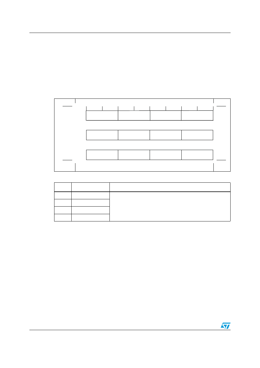
Core peripherals
PM0056
126/154
Doc ID 15491 Rev 3
4.3.7
Interrupt priority registers (NVIC_IPRx)
Address offset: 0x00- 0x0B
Reset value: 0x0000 0000
Required privilege: Privileged
The IPR0-IPR16 registers provide a 4-bit priority field for each interrupt. These registers are
byte-accessible. Each register holds four priority fields, that map to four elements in the
CMSIS interrupt priority array IP[0] to IP[67], as shown in
Figure 19.
NVIC__IPRx register mapping
See
The CMSIS mapping of the Cortex-M3 NVIC registers on page 120
for more
information about the IP[0] to IP[67] interrupt priority array, that provides the software view of
the interrupt priorities.
Find the IPR number and byte offset for interrupt N as follows:
●
The corresponding IPR number, M, is given by M = N DIV 4
●
The byte offset of the required Priority field in this register is N MOD 4, where:
–
byte offset 0 refers to register bits[7:0]
–
byte offset 1 refers to register bits[15:8]
–
byte offset 2 refers to register bits[23:16]
–
byte offset 3 refers to register bits[31:24].
Table 42.
IPR bit assignments
Bits Name
Function
[31:24]
Priority, byte offset 3
Each priority field holds a priority value, 0-255. The lower the value,
the greater the priority of the corresponding interrupt. The processor
implements only bits[7:4] of each field, bits[3:0] read as zero and
ignore writes.
[23:16]
Priority, byte offset 2
[15:8]
Priority, byte offset 1
[7:0]
Priority, byte offset 0
31
24 23
16 15
8 7
0
IP[80]
IPR20
IP[4m+ 3]
IP[4m+ 2]
IP[4m+ 1]
IP[4m]
IPRm
IP[3]
IP[2]
IP[1]
IP[0]
IPR0
. . .
. . .
. . .
. . .
Reserved
Reserved
Reserved
PM0056
Core peripherals
Doc ID 15491 Rev 3
127/154
4.3.8 Software
trigger
interrupt register (NVIC_STIR)
Address offset: 0xE00
Reset value: 0x0000 0000
Required privilege: When the USERSETMPEND bit in the SCR is set to 1, unprivileged
software can access the STIR, see
Section 4.4.5: System control register (SCB_SCR)
. Only
privileged software can enable unprivileged access to the STIR.
4.3.9 Level-sensitive
and pulse interrupts
STM32 interrupts are both level-sensitive and pulse-sensitive. Pulse interrupts are also
described as edge-triggered interrupts.
A level-sensitive interrupt is held asserted until the peripheral deasserts the interrupt signal.
Typically this happens because the ISR accesses the peripheral, causing it to clear the
interrupt request. A pulse interrupt is an interrupt signal sampled synchronously on the
rising edge of the processor clock. To ensure the NVIC detects the interrupt, the peripheral
must assert the interrupt signal for at least one clock cycle, during which the NVIC detects
the pulse and latches the interrupt.
When the processor enters the ISR, it automatically removes the pending state from the
interrupt, see
Hardware and software control of interrupts
. For a level-sensitive interrupt, if
the signal is not deasserted before the processor returns from the ISR, the interrupt
becomes pending again, and the processor must execute its ISR again. This means that the
peripheral can hold the interrupt signal asserted until it no longer needs servicing.
Hardware and software control of interrupts
The Cortex-M3 latches all interrupts. A peripheral interrupt becomes pending for one of the
following reasons:
●
The NVIC detects that the interrupt signal is HIGH and the interrupt is not active
●
The NVIC detects a rising edge on the interrupt signal
●
Software writes to the corresponding interrupt set-pending register bit, see
Section 4.3.4: Interrupt set-pending registers (NVIC_ISPRx)
, or to the STIR to make an
SGI pending, see
Section 4.3.8: Software trigger interrupt register (NVIC_STIR)
31
30
29
28
27
26
25
24
23
22
21
20
19
18
17
16
Reserved
15
14
13
12
11
10
9
8
7
6
5
4
3
2
1
0
Reserved
INTID[8:0]
w
w
w
w
w
w
w
w
w
Bits 31:9 Reserved, must be kept cleared.
Bits 8:0 NTID[8:0] Software generated interrupt ID
Write to the STIR to generate a Software Generated Interrupt (SGI). The value to be written is
the Interrupt ID of the required SGI, in the range 0-239. For example, a value of 0b000000011
specifies interrupt IRQ3.

Core peripherals
PM0056
128/154
Doc ID 15491 Rev 3
A pending interrupt remains pending until one of the following:
●
The processor enters the ISR for the interrupt. This changes the state of the interrupt
from pending to active. Then:
–
For a level-sensitive interrupt, when the processor returns from the ISR, the NVIC
samples the interrupt signal. If the signal is asserted, the state of the interrupt
changes to pending, which might cause the processor to immediately re-enter the
ISR. Otherwise, the state of the interrupt changes to inactive.
–
For a pulse interrupt, the NVIC continues to monitor the interrupt signal, and if this
is pulsed the state of the interrupt changes to pending and active. In this case,
when the processor returns from the ISR the state of the interrupt changes to
pending, which might cause the processor to immediately re-enter the ISR. If the
interrupt signal is not pulsed while the processor is in the ISR, when the processor
returns from the ISR the state of the interrupt changes to inactive.
●
Software writes to the corresponding interrupt clear-pending register bit.
For a level-sensitive interrupt, if the interrupt signal is still asserted, the state of the
interrupt does not change. Otherwise, the state of the interrupt changes to inactive.
For a pulse interrupt, state of the interrupt changes to:
–
Inactive, if the state was pending
–
Active, if the state was active and pending.
4.3.10
NVIC design hints and tips
Ensure software uses correctly aligned register accesses. The processor does not support
unaligned accesses to NVIC registers. See the individual register descriptions for the
supported access sizes.
A interrupt can enter pending state even it is disabled.
Before programming VTOR to relocate the vector table, ensure the vector table entries of
the new vector table are setup for fault handlers, NMI and all enabled exception like
interrupts. For more information see
Section 4.4.3: Vector table offset register (SCB_VTOR)
.
NVIC programming hints
Software uses the CPSIE I and CPSID I instructions to enable and disable interrupts. The
CMSIS provides the following intrinsic functions for these instructions:
void __disable_irq(void) // Disable Interrupts
void __enable_irq(void) // Enable Interrupts
In addition, the CMSIS provides a number of functions for NVIC control, including:
Table 43.
CMSIS functions for NVIC control
CMSIS interrupt control function
Description
void NVIC_SetPriorityGrouping(uint32_t priority_grouping)
Set the priority grouping
void NVIC_EnableIRQ(IRQn_t IRQn)
Enable IRQn
void NVIC_DisableIRQ(IRQn_t IRQn)
Disable IRQn
uint32_t NVIC_GetPendingIRQ (IRQn_t IRQn)
Return true (IRQ-Number) if IRQn is
pending
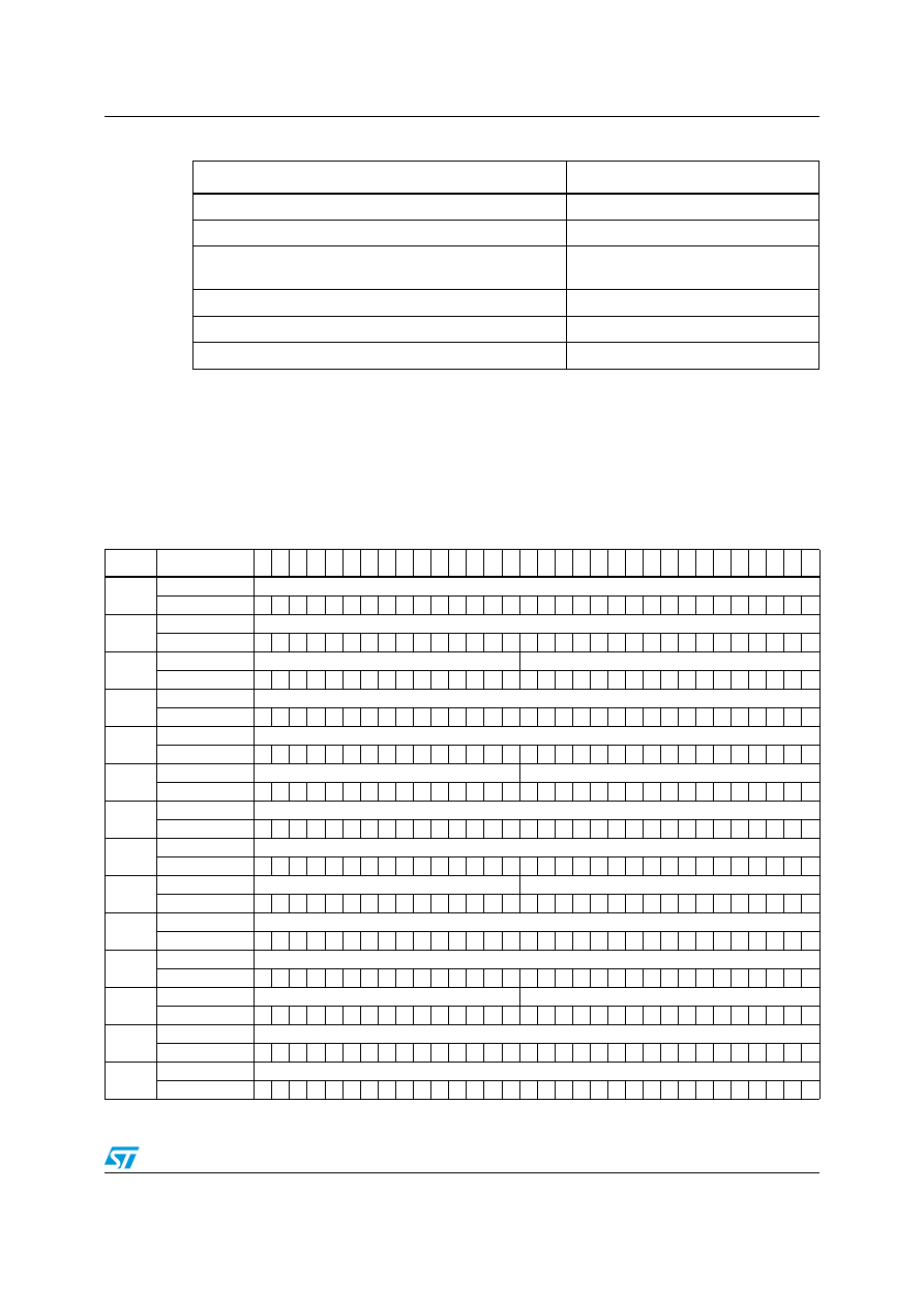
PM0056
Core peripherals
Doc ID 15491 Rev 3
129/154
For more information about these functions see the CMSIS documentation.
4.3.11
NVIC register map
The table provides shows the NVIC register map and reset values. The base address of the
main NVIC register block is 0xE000E100. The NVIC_STIR register is located in a separate
block at 0xE000EF00.
void NVIC_SetPendingIRQ (IRQn_t IRQn)
Set IRQn pending
void NVIC_ClearPendingIRQ (IRQn_t IRQn)
Clear IRQn pending status
uint32_t NVIC_GetActive (IRQn_t IRQn)
Return the IRQ number of the active
interrupt
void NVIC_SetPriority (IRQn_t IRQn, uint32_t priority)
Set priority for IRQn
uint32_t NVIC_GetPriority (IRQn_t IRQn)
Read priority of IRQn
void NVIC_SystemReset (void)
Reset the system
Table 43.
CMSIS functions for NVIC control (continued)
CMSIS interrupt control function
Description
Table 44.
NVIC register map and reset values
Offset
Register
31
30
29
28
27
26
25
24
23
22
21
20
19
18
17
16
15
14
13
12
11
10
9
8
7
6
5
4
3
2
1
0
0x000
NVIC_ISER0
SETENA[31:0]
Reset Value
0
0
0
0
0
0
0
0
0
0
0
0
0
0
0
0
0
0
0
0
0
0
0
0
0
0
0
0
0
0
0
0
0x004
NVIC_ISER1
SETENA[63:32]
Reset Value
0
0
0
0
0
0
0
0
0
0
0
0
0
0
0
0
0
0
0
0
0
0
0
0
0
0
0
0
0
0
0
0
0x008
NVIC_ISER2
Reserved
SETENA [80:64]
Reset Value
0
0
0
0
0
0
0
0
0
0
0
0
0
0
0
0
0
0x080
NVIC_ICER0
CLRENA[31:0]
Reset Value
0
0
0
0
0
0
0
0
0
0
0
0
0
0
0
0
0
0
0
0
0
0
0
0
0
0
0
0
0
0
0
0
0x084
NVIC_ICER1
CLRENA[63:32]
Reset Value
0
0
0
0
0
0
0
0
0
0
0
0
0
0
0
0
0
0
0
0
0
0
0
0
0
0
0
0
0
0
0
0
0x088
NVIC_ICER2
Reserved
CLRENA [80:64]
Reset Value
0
0
0
0
0
0
0
0
0
0
0
0
0
0
0
0
0
0x200
NVIC_ISPR0
SETPEND[31:0]
Reset Value
0
0
0
0
0
0
0
0
0
0
0
0
0
0
0
0
0
0
0
0
0
0
0
0
0
0
0
0
0
0
0
0
0x204
NVIC_ISPR1
SETPEND[63:32]
Reset Value
0
0
0
0
0
0
0
0
0
0
0
0
0
0
0
0
0
0
0
0
0
0
0
0
0
0
0
0
0
0
0
0
0x208
NVIC_ISPR2
Reserved
SETPEND [80:64]
Reset Value
0
0
0
0
0
0
0
0
0
0
0
0
0
0
0
0
0
0x280
NVIC_ICPR0
CLRPEND[31:0]
Reset Value
0
0
0
0
0
0
0
0
0
0
0
0
0
0
0
0
0
0
0
0
0
0
0
0
0
0
0
0
0
0
0
0
0x284
NVIC_ICPR1
CLRPEND[63:32]
Reset Value
0
0
0
0
0
0
0
0
0
0
0
0
0
0
0
0
0
0
0
0
0
0
0
0
0
0
0
0
0
0
0
0
0x288
NVIC_ICPR2
Reserved
CLRPEND [80:64]
Reset Value
0
0
0
0
0
0
0
0
0
0
0
0
0
0
0
0
0
0x300
NVIC_IABR0
ACTIVE[31:0]
Reset Value
0
0
0
0
0
0
0
0
0
0
0
0
0
0
0
0
0
0
0
0
0
0
0
0
0
0
0
0
0
0
0
0
0x304
NVIC_IABR1
ACTIVE[63:32]
Reset Value
0
0
0
0
0
0
0
0
0
0
0
0
0
0
0
0
0
0
0
0
0
0
0
0
0
0
0
0
0
0
0
0
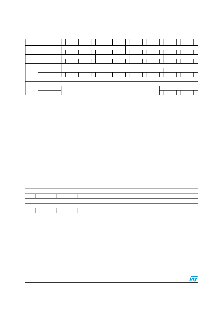
Core peripherals
PM0056
130/154
Doc ID 15491 Rev 3
4.4
System control block (SCB)
The System control block (SCB) provides system implementation information, and system
control. This includes configuration, control, and reporting of the system exceptions. The
CMSIS mapping of the Cortex-M3 SCB registers
To improve software efficiency, the CMSIS simplifies the SCB register presentation. In the
CMSIS, the byte array SHP[0] to SHP[12] corresponds to the registers SHPR1-SHPR3.
4.4.1
CPUID base register (SCB_CPUID)
Address offset: 0x00
Reset value: 0x411F C231
Required privilege: Privileged
The CPUID register contains the processor part number, version, and implementation
information.
0x308
NVIC_IABR2
Reserved
ACTIVE [80:64]
Reset Value
0
0
0
0
0
0
0
0
0
0
0
0
0
0
0
0
0
0x400
NVIC_IPR0
IP[3]
IP[2]
IP[1]
IP[0]
Reset Value
0
0
0
0
0
0
0
0
0
0
0
0
0
0
0
0
0
0
0
0
0
0
0
0
0
0
0
0
0
0
0
0
:
:
:
0x420
NVIC_IPR20
Reserved
IP[80]
Reset Value
0
0
0
0
0
0
0
0
0
0
0
0
0
0
0
0
0
0
0
0
0
0
0
0
0
0
0
0
0
0
0
0
SCB registers
Reserved
0xE00
NVIC_STIR
Reserved
INTID[8:0]
Reset Value
0
0
0
0
0
0
0
0
0
Table 44.
NVIC register map and reset values (continued)
Offset
Register
31
30
29
28
27
26
25
24
23
22
21
20
19
18
17
16
15
14
13
12
11
10
9
8
7
6
5
4
3
2
1
0
31
30
29
28
27
26
25
24
23
22
21
20
19
18
17
16
Implementer
Variant
Constant
r
r
r
r
r
r
r
r
r
r
r
r
r
r
r
r
15
14
13
12
11
10
9
8
7
6
5
4
3
2
1
0
PartNo
Revision
r
r
r
r
r
r
r
r
r
r
r
r
r
r
r
r
Bits 31:24 Implementer: Implementer code
0x41: ARM
Bits 23:20 Variant: Variant number
The r value in the rnpn product revision identifier
0x1: r1p1
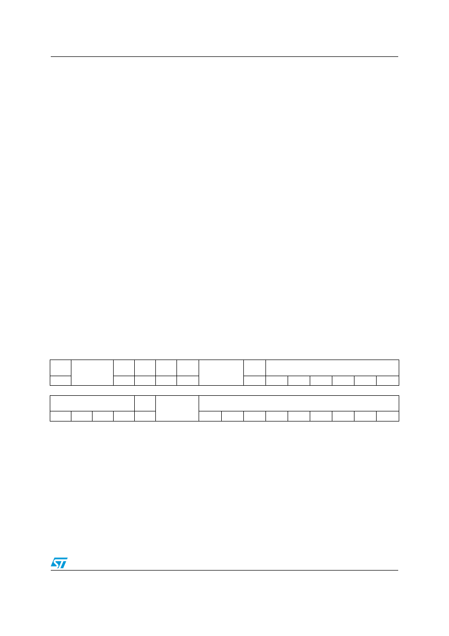
PM0056
Core peripherals
Doc ID 15491 Rev 3
131/154
4.4.2
Interrupt control and state register (SCB_ICSR)
Address offset: 0x04
Reset value: 0x0000 0000
Required privilege: Privileged
The ICSR:
●
Provides:
–
A set-pending bit for the Non-Maskable Interrupt (NMI) exception
–
Set-pending and clear-pending bits for the PendSV and SysTick exceptions
●
Indicates:
–
The exception number of the exception being processed
–
Whether there are preempted active exceptions
–
The exception number of the highest priority pending exception
–
Whether any interrupts are pending.
Caution:
When you write to the ICSR, the effect is unpredictable if you:
●
Write 1 to the PENDSVSET bit and write 1 to the PENDSVCLR bit
●
Write 1 to the PENDSTSET bit and write 1 to the PENDSTCLR bit.
Bits 19:16 Constant: Reads as 0xF
Bits 15:4 PartNo: Part number of the processor
0xC23: = Cortex-M3
Bits 3:0 Revision: Revision number
The p value in the rnpn product revision identifier
0x1: = r1p1
31
30
29
28
27
26
25
24
23
22
21
20
19
18
17
16
NMIPE
NDSET
Reserved
PEND
SVSET
PEND
SVCLR
PEND
STSET
PENDS
TCLR
Reserved
ISRPE
NDING
VECTPENDING[9:4]
rw
rw
w
rw
w
r
r
r
r
r
r
r
15
14
13
12
11
10
9
8
7
6
5
4
3
2
1
0
VECTPENDING[3:0]
RETOB
ASE
Reserved
VECTACTIVE[8:0]
r
r
r
r
r
rw
rw
rw
rw
rw
rw
rw
rw
rw

Core peripherals
PM0056
132/154
Doc ID 15491 Rev 3
Bit 31 NMIPENDSET: NMI set-pending bit.
Write:
0: No effect
1: Change NMI exception state to pending.
Read:
0: NMI exception is not pending
1: NMI exception is pending
Because NMI is the highest-priority exception, normally the processor enter the NMI
exception handler as soon as it registers a write of 1 to this bit, and entering the handler clears
this bit to 0. A read of this bit by the NMI exception handler returns 1 only if the NMI signal is
reasserted while the processor is executing that handler.
Bits 30:29 Reserved, must be kept cleared
Bit 28 PENDSVSET: PendSV set-pending bit.
Write:
0: No effect
1: Change PendSV exception state to pending.
Read:
0: PendSV exception is not pending
1: PendSV exception is pending
Writing 1 to this bit is the only way to set the PendSV exception state to pending.
Bit 27 PENDSVCLR: PendSV clear-pending bit.
Write:
0: No effect
1: Removes the pending state from the PendSV exception.
Bit 26 PENDSTSET: SysTick exception set-pending bit.
Write:
0: No effect
1: Change SysTick exception state to pending
Read:
0: SysTick exception is not pending
1: SysTick exception is pending
Bit 25 PENDSTCLR: SysTick exception clear-pending bit.
Write:
0: No effect
1: Removes the pending state from the SysTick exception.
This bit is write-only. On a register read its value is unknown.
Bit 24 Reserved, must be kept cleared.
Bit 23 This bit is reserved for Debug use and reads-as-zero when the processor is not in Debug.
Bit 22 ISRPENDING: Interrupt pending flag, excluding NMI and Faults
0: Interrupt not pending
1: Interrupt pending
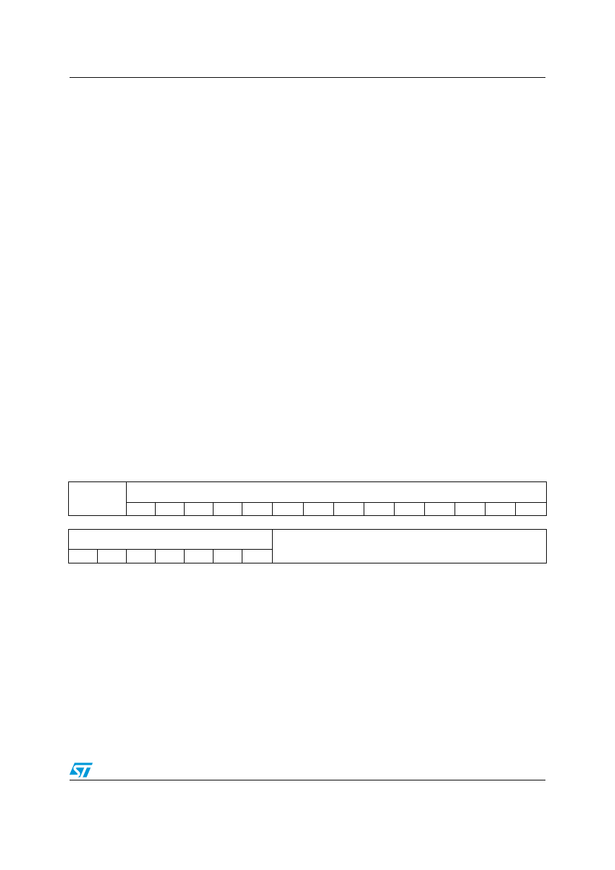
PM0056
Core peripherals
Doc ID 15491 Rev 3
133/154
4.4.3 Vector
table
offset register (SCB_VTOR)
Address offset: 0x08
Reset value: 0x0000 0000
Required privilege: Privileged
Bits 21:12 VECTPENDING[9:0] Pending vector
Indicates the exception number of the highest priority pending enabled exception.
0: No pending exceptions
Other values: The exception number of the highest priority pending enabled exception.
The value indicated by this field includes the effect of the BASEPRI and FAULTMASK
registers, but not any effect of the PRIMASK register.
Bit 11 RETOBASE: Return to base level
Indicates whether there are preempted active exceptions:
0: There are preempted active exceptions to execute
1: There are no active exceptions, or the currently-executing exception is the only active
exception.
Bits 10:9 Reserved, must be kept cleared
Bits 8:0 VECTACTIVE[8:0] Active vector
Contains the active exception number:
0: Thread mode
Other values: The exception number
(1)
of the currently active exception.
Note: Subtract 16 from this value to obtain the IRQ number required to index into the
Interrupt Clear-Enable, Set-Enable, Clear-Pending, Set-Pending, or Priority Registers,
see
1.
This is the same value as IPSR bits[8:0], see
Interrupt program status register on page 19
.
31
30
29
28
27
26
25
24
23
22
21
20
19
18
17
16
Reserved
TBLOFF[29:16]
rw
rw
rw
rw
rw
rw
rw
rw
rw
rw
rw
rw
rw
rw
15
14
13
12
11
10
9
8
7
6
5
4
3
2
1
0
TBLOFF[15:9]
Reserved
rw
rw
rw
rw
rw
rw
rw
Bits 31:30 Reserved, must be kept cleared
Bits 29:11 TBLOFF[29:9]: Vector table base offset field.
It contains bits [29:9] of the offset of the table base from memory address 0x00000000. When
setting TBLOFF, you must align the offset to the number of exception entries in the vector table.
The minimum alignment is 128 words. Table alignment requirements mean that bits[8:0] of the
table offset are always zero.
Bit 29 determines whether the vector table is in the code or SRAM memory region.
0: Code
1: SRAM
Note: Bit 29 is sometimes called the TBLBASE bit.
Bits 10:0 Reserved, must be kept cleared
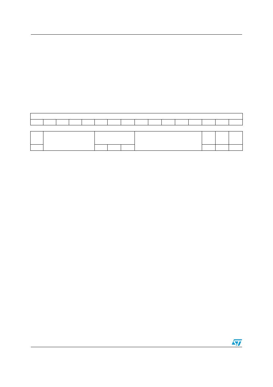
Core peripherals
PM0056
134/154
Doc ID 15491 Rev 3
4.4.4
Application interrupt and reset control register (SCB_AIRCR)
Address offset: 0x0C
Reset value: 0xFA05 0000
Required privilege: Privileged
The AIRCR provides priority grouping control for the exception model, endian status for data
accesses, and reset control of the system.
To write to this register, you must write 0x5FA to the VECTKEY field, otherwise the
processor ignores the write.
Binary point
The PRIGROUP field indicates the position of the binary point that splits the PRI_n fields in
the Interrupt Priority Registers into separate group priority and subpriority fields.
shows how the PRIGROUP value controls this split.
31
30
29
28
27
26
25
24
23
22
21
20
19
18
17
16
VECTKEYSTAT[15:0](read)/ VECTKEY[15:0](write)
rw
rw
rw
rw
rw
rw
rw
rw
rw
rw
rw
rw
rw
rw
rw
rw
15
14
13
12
11
10
9
8
7
6
5
4
3
2
1
0
ENDIA
NESS
Reserved
PRIGROUP
Reserved
SYS
RESET
REQ
VECT
CLR
ACTIVE
VECT
RESET
r
rw
rw
rw
w
w
w
Bits 31:16 VECTKEYSTAT[15:0]/ VECTKEY[15:0] Register key
Reads as 0xFA05
On writes, write 0x5FA to VECTKEY, otherwise the write is ignored.
Bit 15 ENDIANESS Data endianness bit
Reads as 0.
0: Little-endian
Bits 14:11 Reserved, must be kept cleared
Bits 10:8 PRIGROUP[2:0]: Interrupt priority grouping field
This field determines the split of group priority from subpriority, see
.
Bits 7:3 Reserved, must be kept cleared
Bit 2 SYSRESETREQ System reset request
This is intended to force a large system reset of all major components except for debug.
This bit reads as 0.
0: No system reset request
1: Asserts a signal to the outer system that requests a reset.
Bit 1 VECTCLRACTIVE
Reserved for Debug use. This bit reads as 0. When writing to the register you must write 0 to
this bit, otherwise behavior is unpredictable.
Bit 0 VECTRESET
Reserved for Debug use. This bit reads as 0. When writing to the register you must write 0 to
this bit, otherwise behavior is unpredictable.
PM0056
Core peripherals
Doc ID 15491 Rev 3
135/154
Determining preemption of an exception uses only the group priority field, see
Interrupt priority grouping on page 38
.
4.4.5 System
control
register (SCB_SCR)
Address offset: 0x10
Reset value: 0x0000 0000
Required privilege: Privileged
The SCR controls features of entry to and exit from low power state.
Table 45.
Priority grouping
PRIGROUP
[2:0]
Interrupt priority level value, PRI_N[7:4]
Number of
Binary
point
(1)
1.
PRI_n[7:4] field showing the binary point. x denotes a group priority field bit, and y denotes a subpriority
field bit.
Group priority
bits
Subpriority
bits
Group
priorities
Sub
priorities
0b011
0bxxxx
[7:4]
None
16
None
0b100
0bxxx.y
[7:5]
[4]
8
2
0b101
0bxx.yy
[7:6]
[5:4]
4
4
0b110
0bx.yyy
[7]
[6:4]
2
8
0b111
0b.yyyy
None
[7:4]
None
16
31
30
29
28
27
26
25
24
23
22
21
20
19
18
17
16
Reserved
15
14
13
12
11
10
9
8
7
6
5
4
3
2
1
0
Reserved
SEVON
PEND
Res.
SLEEP
DEEP
SLEEP
ON
EXIT
Res.
rw
rw
rw
Bits 31:5 Reserved, must be kept cleared
Bit 4 SEVEONPEND Send Event on Pending bit
When an event or interrupt enters pending state, the event signal wakes up the processor from
WFE. If the processor is not waiting for an event, the event is registered and affects the next
WFE.
The processor also wakes up on execution of an SEV instruction or an external event
0: Only enabled interrupts or events can wakeup the processor, disabled interrupts are
excluded
1: Enabled events and all interrupts, including disabled interrupts, can wakeup the
processor.
Bit 3 Reserved, must be kept cleared
Core peripherals
PM0056
136/154
Doc ID 15491 Rev 3
4.4.6
Configuration and control register (SCB_CCR)
Address offset: 0x14
Reset value: 0x0000 0200
Required privilege: Privileged
The CCR controls entry to Thread mode and enables:
●
The handlers for NMI, hard fault and faults escalated by FAULTMASK to ignore bus
faults
●
Trapping of divide by zero and unaligned accesses
●
Access to the STIR by unprivileged software, see
Software trigger interrupt register
Bit 2 SLEEPDEEP
Controls whether the processor uses sleep or deep sleep as its low power mode:
0: Sleep
1: Deep sleep.
Bit 2 SLEEPONEXIT
Configures sleep-on-exit when returning from Handler mode to Thread mode. Setting this bit to
1 enables an interrupt-driven application to avoid returning to an empty main application.
0: Do not sleep when returning to Thread mode.
1: Enter sleep, or deep sleep, on return from an interrupt service routine.
Bit 0 Reserved, must be kept cleared
31
30
29
28
27
26
25
24
23
22
21
20
19
18
17
16
Reserved
15
14
13
12
11
10
9
8
7
6
5
4
3
2
1
0
Reserved
STK
ALIGN
BFHF
NMIGN
Reserved
DIV_0_
TRP
UN
ALIGN_
TRP
Res.
USER
SET
MPEND
NON
BASE
THRD
ENA
rw
rw
rw
rw
rw
rw
Bits 31:10 Reserved, must be kept cleared
Bit 9 STKALIGN
Configures stack alignment on exception entry. On exception entry, the processor uses bit 9 of
the stacked PSR to indicate the stack alignment. On return from the exception it uses this
stacked bit to restore the correct stack alignment.
0: 4-byte aligned
1: 8-byte aligned
Bit 8 BFHFNMIGN
Enables handlers with priority -1 or -2 to ignore data bus faults caused by load and store
instructions. This applies to the hard fault, NMI, and FAULTMASK escalated handlers. Set this
bit to 1 only when the handler and its data are in absolutely safe memory. The normal use of
this bit is to probe system devices and bridges to detect control path problems and fix them.
0: Data bus faults caused by load and store instructions cause a lock-up
1: Handlers running at priority -1 and -2 ignore data bus faults caused by load and store
instructions.
PM0056
Core peripherals
Doc ID 15491 Rev 3
137/154
4.4.7 System
handler
priority registers (SHPRx)
The SHPR1-SHPR3 registers set the priority level, 0 to 15 of the exception handlers that
have configurable priority.
SHPR1-SHPR3 are byte accessible.
The system fault handlers and the priority field and register for each handler are:
Each PRI_N field is 8 bits wide, but the processor implements only bits[7:4] of each field,
and bits[3:0] read as zero and ignore writes.
Bits 7:5 Reserved, must be kept cleared
Bit 4 DIV_0_TRP
Enables faulting or halting when the processor executes an SDIV or UDIV instruction with a
divisor of 0:
0: Do not trap divide by 0
1: Trap divide by 0.
When this bit is set to 0, a divide by zero returns a quotient of 0.
Bit 3 UNALIGN_ TRP
Enables unaligned access traps:
0: Do not trap unaligned halfword and word accesses
1: Trap unaligned halfword and word accesses.
If this bit is set to 1, an unaligned access generates a usage fault.
Unaligned LDM, STM, LDRD, and STRD instructions always fault irrespective of whether
UNALIGN_TRP is set to 1.
Bit 2 Reserved, must be kept cleared
Bit 1 USERSETMPEND
Enables unprivileged software access to the STIR, see
Software trigger interrupt register
0: Disable
1: Enable.
Bit 0 NONBASETHRDENA
Configures how the processor enters Thread mode.
0: Processor can enter Thread mode only when no exception is active.
1: Processor can enter Thread mode from any level under the control of an EXC_RETURN
value, see
Table 46.
System fault handler priority fields
Handler
Field
Register description
Memory management fault
PRI_4
System handler priority register 1 (SCB_SHPR1)
Bus fault
PRI_5
Usage fault
PRI_6
SVCall
PRI_11
System handler priority register 2 (SCB_SHPR2) on
page 138
PendSV
PRI_14
System handler priority register 3 (SCB_SHPR3) on
page 139
SysTick
PRI_15
Core peripherals
PM0056
138/154
Doc ID 15491 Rev 3
System handler priority register 1 (
SCB_
SHPR1)
Address offset: 0x18
Reset value: 0x0000 0000
Required privilege: Privileged
System handler priority register 2 (
SCB_
SHPR2)
Address offset: 0x1C
Reset value: 0x0000 0000
Required privilege: Privileged
31
30
29
28
27
26
25
24
23
22
21
20
19
18
17
16
Reserved
PRI_6[7:4]
PRI_6[3:0]
rw
rw
rw
rw
r
r
r
r
15
14
13
12
11
10
9
8
7
6
5
4
3
2
1
0
PRI_5[7:4]
PRI_5[3:0]
PRI_4[7:4]
PRI_4[7:4]
rw
rw
rw
rw
r
r
r
r
rw
rw
rw
rw
r
r
r
r
Bits 31:24 Reserved, must be kept cleared
Bits 23:16 PRI_6[7:0]: Priority of system handler 6, usage fault
Bits 15:8 PRI_5[7:0]: Priority of system handler 5, bus fault
Bits 7:0 PRI_4[7:0]: Priority of system handler 4, memory management fault
31
30
29
28
27
26
25
24
23
22
21
20
19
18
17
16
PRI_11[7:4]
PRI_11[3:0]
Reserved
rw
rw
rw
rw
r
r
r
r
15
14
13
12
11
10
9
8
7
6
5
4
3
2
1
0
Reserved
Bits 31:24 PRI_11[7:0]: Priority of system handler 11, SVCall
Bits 23:0 Reserved, must be kept cleared

PM0056
Core peripherals
Doc ID 15491 Rev 3
139/154
System handler priority register 3 (
SCB_
SHPR3)
Address: 0xE000 ED20
Reset value: 0x0000 0000
Required privilege: Privileged
4.4.8 System
handler
control
and state register (SCB_SHCSR)
Address offset: 0x24
Reset value: 0x0000 0000
Required privilege: Privileged
The SHCSR enables the system handlers, and indicates:
●
The pending status of the bus fault, memory management fault, and SVC exceptions
●
The active status of the system handlers.
If you disable a system handler and the corresponding fault occurs, the processor treats the
fault as a hard fault.
You can write to this register to change the pending or active status of system exceptions.
An OS kernel can write to the active bits to perform a context switch that changes the
current exception type.
●
Software that changes the value of an active bit in this register without correct
adjustment to the stacked content can cause the processor to generate a fault
exception. Ensure software that writes to this register retains and subsequently
restores the current active status.
●
After you have enabled the system handlers, if you have to change the value of a bit in
this register you must use a read-modify-write procedure to ensure that you change
only the required bit.
31
30
29
28
27
26
25
24
23
22
21
20
19
18
17
16
PRI_15[7:4]
PRI_15[3:0]
PRI_14[7:4]
PRI_14[3:0]
rw
rw
rw
rw
r
r
r
r
rw
rw
rw
rw
r
r
r
r
15
14
13
12
11
10
9
8
7
6
5
4
3
2
1
0
Reserved
Bits 31:24 PRI_15[7:0]: Priority of system handler 15, SysTick exception
Bits 23:16 PRI_14[7:0]: Priority of system handler 14, PendSV
Bits 15:0 Reserved, must be kept cleared

Core peripherals
PM0056
140/154
Doc ID 15491 Rev 3
31
30
29
28
27
26
25
24
23
22
21
20
19
18
17
16
Reserved
USG
FAULT
ENA
BUS
FAULT
ENA
MEM
FAULT
ENA
rw
rw
rw
15
14
13
12
11
10
9
8
7
6
5
4
3
2
1
0
SV
CALL
PEND
ED
BUS
FAULT
PEND
ED
MEM
FAULT
PEND
ED
USG
FAULT
PEND
ED
SYS
TICK
ACT
PEND
SV
ACT
Res.
MONIT
OR
ACT
SV
CALL
ACT
Reserved
USG
FAULT
ACT
Res.
BUS
FAULT
ACT
MEM
FAULT
ACT
rw
rw
rw
rw
rw
rw
rw
rw
rw
rw
rw
Bits 31:19 Reserved, must be kept cleared
Bit 18 USGFAULTENA: Usage fault enable bit, set to 1 to enable
(1)
Bit 17 BUSFAULTENA: Bus fault enable bit, set to 1 to enable
Bit 16 MEMFAULTENA: Memory management fault enable bit, set to 1 to enable
Bit 15 SVCALLPENDED: SVC call pending bit, reads as 1 if exception is pending
(2)
Bit 14 BUSFAULTPENDED: Bus fault exception pending bit, reads as 1 if exception is pending
Bit 13 MEMFAULTPENDED: Memory management fault exception pending bit, reads as 1 if
exception is pending
Bit 12 USGFAULTPENDED: Usage fault exception pending bit, reads as 1 if exception is pending
Bit 11 SYSTICKACT: SysTick exception active bit, reads as 1 if exception is active
(3)
Bit 10 PENDSVACT: PendSV exception active bit, reads as 1 if exception is active
Bit 9 Reserved, must be kept cleared
Bit 8 MONITORACT: Debug monitor active bit, reads as 1 if Debug monitor is active
Bit 7 SVCALLACT: SVC call active bit, reads as 1 if SVC call is active
Bits 6:4 Reserved, must be kept cleared
Bit 3 USGFAULTACT: Usage fault exception active bit, reads as 1 if exception is active
Bit 2 Reserved, must be kept cleared
Bit 1 BUSFAULTACT: Bus fault exception active bit, reads as 1 if exception is active
Bit 0 MEMFAULTACT: Memory management fault exception active bit, reads as 1 if exception is
active
1.
Enable bits, set to 1 to enable the exception, or set to 0 to disable the exception.
2.
Pending bits, read as 1 if the exception is pending, or as 0 if it is not pending. You can write to these bits to change the
pending status of the exceptions.
3.
Active bits, read as 1 if the exception is active, or as 0 if it is not active. You can write to these bits to change the active
status of the exceptions, but see the Caution in this section.
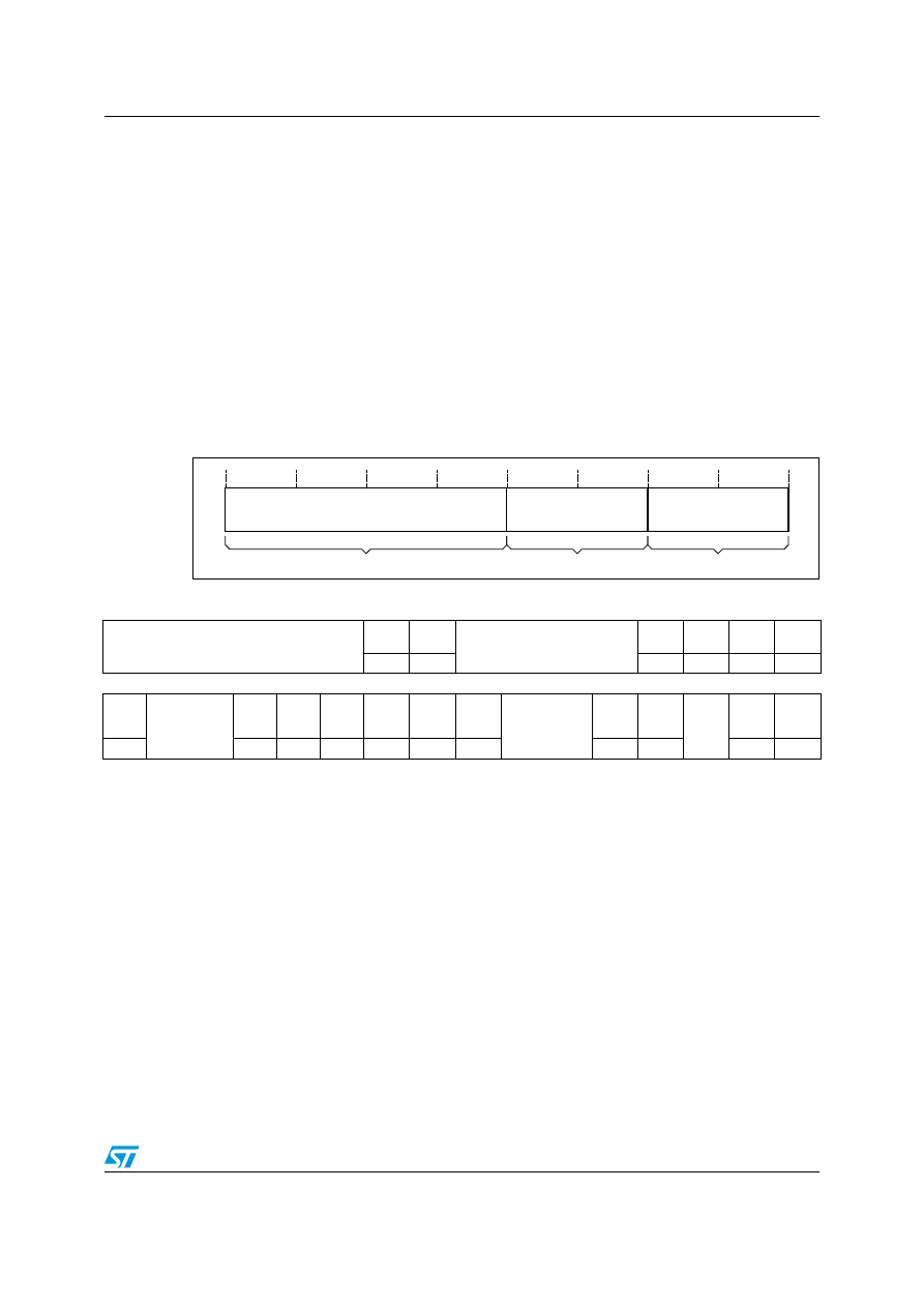
PM0056
Core peripherals
Doc ID 15491 Rev 3
141/154
4.4.9 Configurable
fault
status register (SCB_CFSR)
Address offset: 0x28
Reset value: 0x0000 0000
Required privilege: Privileged
The CFSR is byte accessible. You can access the CFSR or its subregisters as follows:
●
Access the complete CFSR with a word access to 0xE000ED28
●
Access the MMFSR with a byte access to 0xE000ED28
●
Access the MMFSR and BFSR with a halfword access to 0xE000ED28
●
Access the BFSR with a byte access to 0xE000ED29
●
Access the UFSR with a halfword access to 0xE000ED2A.
The CFSR indicates the cause of a memory management fault, bus fault, or usage fault.
Figure 20.
CFSR subregisters
Memory Management
Fault Status Register
31
16 15
8 7
0
Usage Fault Status Register
Bus Fault Status
Register
UFSR
BFSR
MMFSR
31
30
29
28
27
26
25
24
23
22
21
20
19
18
17
16
Reserved
DIVBY
ZERO
UNALI
GNED
Reserved
NOCP
INVPC
INV
STATE
UNDEF
INSTR
rc_w1
rc_w1
rc_w1
rc_w1
rc_w1
rc_w1
15
14
13
12
11
10
9
8
7
6
5
4
3
2
1
0
BFARV
ALID
Reserved
STK
ERR
UNSTK
ERR
IMPRE
CIS
ERR
PRECI
S ERR
IBUS
ERR
MMAR
VALID
Reserved
MSTK
ERR
M
UNSTK
ERR
Res.
DACC
VIOL
IACC
VIOL
rw
rw
rw
rw
rw
rw
rw
rw
rw
rw
rw
Bits 31:26 Reserved, must be kept cleared
Bit 25 DIVBYZERO: Divide by zero usage fault
When the processor sets this bit to 1, the PC value stacked for the exception return points to
the instruction that performed the divide by zero.
Enable trapping of divide by zero by setting the DIV_0_TRP bit in the CCR to 1, see
Configuration and control register (SCB_CCR) on page 136
.
0: No divide by zero fault, or divide by zero trapping not enabled
1: The processor has executed an SDIV or UDIV instruction with a divisor of 0.
Bit 24 UNALIGNED: Unaligned access usage fault:
Enable trapping of unaligned accesses by setting the UNALIGN_TRP bit in the CCR to 1, see
Configuration and control register (SCB_CCR) on page 136
.
Unaligned LDM, STM, LDRD, and STRD instructions always fault irrespective of the setting of
UNALIGN_TRP.
0: No unaligned access fault, or unaligned access trapping not enabled
1: the processor has made an unaligned memory access.
Bits 23:20 Reserved, must be kept cleared

Core peripherals
PM0056
142/154
Doc ID 15491 Rev 3
Bit 19 NOCP: No coprocessor usage fault. The processor does not support coprocessor instructions:
0: No usage fault caused by attempting to access a coprocessor
1: the processor has attempted to access a coprocessor.
Bit 18 INVPC: Invalid PC load usage fault, caused by an invalid PC load by EXC_RETURN:
When this bit is set to 1, the PC value stacked for the exception return points to the instruction
that tried to perform the illegal load of the PC.
0: No invalid PC load usage fault
1: The processor has attempted an illegal load of EXC_RETURN to the PC, as a result of an
invalid context, or an invalid EXC_RETURN value.
Bit 17 INVSTATE: Invalid state usage fault:
When this bit is set to 1, the PC value stacked for the exception return points to the instruction
that attempted the illegal use of the EPSR.
This bit is not set to 1 if an undefined instruction uses the EPSR.
0: No invalid state usage fault
1: The processor has attempted to execute an instruction that makes illegal use of the
EPSR.
Bit 16 UNDEFINSTR: Undefined instruction usage fault:
When this bit is set to 1, the PC value stacked for the exception return points to the undefined
instruction.
An undefined instruction is an instruction that the processor cannot decode.
0: No undefined instruction usage fault
1: The processor has attempted to execute an undefined instruction.
Bit 15 BFARVALID: Bus Fault Address Register (BFAR) valid flag:
The processor sets this bit to 1 after a bus fault where the address is known. Other faults can
set this bit to 0, such as a memory management fault occurring later.
If a bus fault occurs and is escalated to a hard fault because of priority, the hard fault handler
must set this bit to 0. This prevents problems if returning to a stacked active bus fault handler
whose BFAR value has been overwritten.
0: Value in BFAR is not a valid fault address
1: BFAR holds a valid fault address.
Bits 14:13 Reserved, must be kept cleared
Bit 12 STKERR: Bus fault on stacking for exception entry
When the processor sets this bit to 1, the SP is still adjusted but the values in the context area
on the stack might be incorrect. The processor does not write a fault address to the BFAR.
0: No stacking fault
1: Stacking for an exception entry has caused one or more bus faults.
Bit 11 UNSTKERR: Bus fault on unstacking for a return from exception
This fault is chained to the handler. This means that when the processor sets this bit to 1, the
original return stack is still present. The processor does not adjust the SP from the failing
return, does not performed a new save, and does not write a fault address to the BFAR.
0: No unstacking fault
1: Unstack for an exception return has caused one or more bus faults.

PM0056
Core peripherals
Doc ID 15491 Rev 3
143/154
Bit 10 IMPRECISERR: Imprecise data bus error
When the processor sets this bit to 1, it does not write a fault address to the BFAR.
This is an asynchronous fault. Therefore, if it is detected when the priority of the current
process is higher than the bus fault priority, the bus fault becomes pending and becomes
active only when the processor returns from all higher priority processes. If a precise fault
occurs before the processor enters the handler for the imprecise bus fault, the handler detects
both IMPRECISERR set to 1 and one of the precise fault status bits set to 1.
0: No imprecise data bus error
1: A data bus error has occurred, but the return address in the stack frame is not related to
the instruction that caused the error.
Bit 9 PRECISERR: Precise data bus error
When the processor sets this bit is 1, it writes the faulting address to the BFAR.
0: No precise data bus error
1: A data bus error has occurred, and the PC value stacked for the exception return points to
the instruction that caused the fault.
Bit 8 IBUSERR: Instruction bus error
The processor detects the instruction bus error on prefetching an instruction, but it sets the
IBUSERR flag to 1 only if it attempts to issue the faulting instruction.
When the processor sets this bit is 1, it does not write a fault address to the BFAR.
0: No instruction bus error
1: Instruction bus error.
Bit 7 MMARVALID: Memory Management Fault Address Register (MMAR) valid flag
If a memory management fault occurs and is escalated to a hard fault because of priority, the
hard fault handler must set this bit to 0. This prevents problems on return to a stacked active
memory management fault handler whose MMAR value has been overwritten.
0: Value in MMAR is not a valid fault address
1: MMAR holds a valid fault address.
Bits 6:5 Reserved, must be kept cleared
Bit 4 MSTKERR: Memory manager fault on stacking for exception entry
When this bit is 1, the SP is still adjusted but the values in the context area on the stack might
be incorrect. The processor has not written a fault address to the MMAR.
0: No stacking fault
1: Stacking for an exception entry has caused one or more access violations.
Bit 3 MUNSTKERR: Memory manager fault on unstacking for a return from exception
This fault is chained to the handler. This means that when this bit is 1, the original return stack
is still present. The processor has not adjusted the SP from the failing return, and has not
performed a new save. The processor has not written a fault address to the MMAR.
0: No unstacking fault
1: Unstack for an exception return has caused one or more access violations.
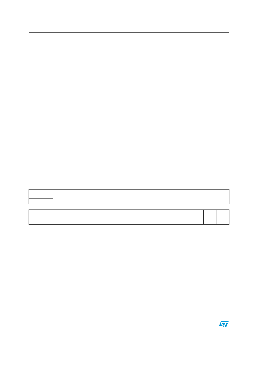
Core peripherals
PM0056
144/154
Doc ID 15491 Rev 3
4.4.10 Hard
fault
status register (SCB_HFSR)
Address offset: 0x2C
Reset value: 0x0000 0000
Required privilege: Privileged
The HFSR gives information about events that activate the hard fault handler.
This register is read, write to clear. This means that bits in the register read normally, but
writing 1 to any bit clears that bit to 0.
Bit 2 Reserved, must be kept cleared
Bit 1 DACCVIOL: Data access violation flag
When this bit is 1, the PC value stacked for the exception return points to the faulting
instruction. The processor has loaded the MMAR with the address of the attempted access.
0: No data access violation fault
1: The processor attempted a load or store at a location that does not permit the operation.
Bit 1 IACCVIOL: Instruction access violation flag
This fault occurs on any access to an XN region.
When this bit is 1, the PC value stacked for the exception return points to the faulting
instruction. The processor has not written a fault address to the MMAR.
0: No instruction access violation fault
1: The processor attempted an instruction fetch from a location that does not permit
execution.
31
30
29
28
27
26
25
24
23
22
21
20
19
18
17
16
DEBU
G_VT
FORC
ED
Reserved
rc_w1
rc_w1
15
14
13
12
11
10
9
8
7
6
5
4
3
2
1
0
Reserved
VECT
TBL
Res.
rc_w1
Bit 31 DEBUG_VT:
Reserved for Debug use. When writing to the register you must write 0 to this bit, otherwise
behavior is unpredictable.
Bit 30 FORCED: Forced hard fault
Indicates a forced hard fault, generated by escalation of a fault with configurable priority that
cannot be handles, either because of priority or because it is disabled:
When this bit is set to 1, the hard fault handler must read the other fault status registers to find
the cause of the fault.
0: No forced hard fault
1: Forced hard fault.

PM0056
Core peripherals
Doc ID 15491 Rev 3
145/154
Bits 29:2 Reserved, must be kept cleared
Bit 1 VECTTBL: Vector table hard fault
Indicates a bus fault on a vector table read during exception processing:
This error is always handled by the hard fault handler.
When this bit is set to 1, the PC value stacked for the exception return points to the instruction
that was preempted by the exception.
0: No bus fault on vector table read
1: Bus fault on vector table read.
Bit 0 Reserved, must be kept cleared
Core peripherals
PM0056
146/154
Doc ID 15491 Rev 3
4.4.11 Memory
management
fault address register (SCB_MMFAR)
Address offset: 0x34
Reset value: undefined
Required privilege: Privileged
4.4.12 Bus
fault
address register (SCB_BFAR)
Address offset: 0x38
Reset value: undefined
Required privilege: Privileged
31
30
29
28
27
26
25
24
23
22
21
20
19
18
17
16
MMFAR[31:16]
rw
rw
rw
rw
rw
rw
rw
rw
rw
rw
rw
rw
rw
rw
rw
rw
15
14
13
12
11
10
9
8
7
6
5
4
3
2
1
0
MMFAR[15:0]
rw
rw
rw
rw
rw
rw
rw
rw
rw
rw
rw
rw
rw
rw
rw
rw
Bits 31:0 MMFAR[31:0]: Memory management fault address
When the MMARVALID bit of the MMFSR is set to 1, this field holds the address of the
location that generated the memory management fault.
When an unaligned access faults, the address is the actual address that faulted. Because a
single read or write instruction can be split into multiple aligned accesses, the fault address
can be any address in the range of the requested access size.
Flags in the MMFSR register indicate the cause of the fault, and whether the value in the
MMFAR is valid. See
Configurable fault status register (SCB_CFSR) on page 141
.
31
30
29
28
27
26
25
24
23
22
21
20
19
18
17
16
BFAR[31:16]
rw
rw
rw
rw
rw
rw
rw
rw
rw
rw
rw
rw
rw
rw
rw
rw
15
14
13
12
11
10
9
8
7
6
5
4
3
2
1
0
BFAR[15:0]
rw
rw
rw
rw
rw
rw
rw
rw
rw
rw
rw
rw
rw
rw
rw
rw
Bits 31:0 BFAR[31:0]: Bus fault address
When the BFARVALID bit of the BFSR is set to 1, this field holds the address of the location
that generated the bus fault.
When an unaligned access faults the address in the BFAR is the one requested by the
instruction, even if it is not the address of the fault.
Flags in the BFSR register indicate the cause of the fault, and whether the value in the BFAR
is valid. See
Configurable fault status register (SCB_CFSR) on page 141
.
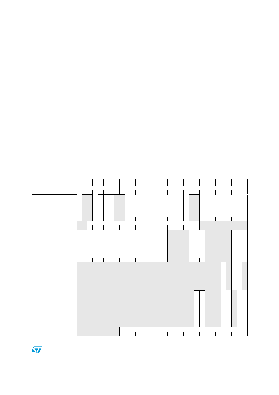
PM0056
Core peripherals
Doc ID 15491 Rev 3
147/154
4.4.13
System control block design hints and tips
Ensure software uses aligned accesses of the correct size to access the system control
block registers:
●
except for the CFSR and SHPR1-SHPR3, it must use aligned word accesses
●
for the CFSR and SHPR1-SHPR3 it can use byte or aligned halfword or word
accesses.
The processor does not support unaligned accesses to system control block registers.
In a fault handler. to determine the true faulting address:
1.
Read and save the MMFAR or BFAR value.
2.
Read the MMARVALID bit in the MMFSR, or the BFARVALID bit in the BFSR. The
MMFAR or BFAR address is valid only if this bit is 1.
Software must follow this sequence because another higher priority exception might change
the MMFAR or BFAR value. For example, if a higher priority handler preempts the current
fault handler, the other fault might change the MMFAR or BFAR value.
4.4.14
SCB register map
The table provides shows the System control block register map and reset values. The base
address of the SCB register block is 0xE000 ED00.
Table 47.
SCB register map and reset values
Offset
Register
31
30
29
28
27
26
25
24
23
22
21
20
19
18
17
16
15
14
13
12
11
10
9
8
7
6
5
4
3
2
1
0
0x00
SCB_CPUID
Implementer
Variant
Constant
PartNo
Revision
Reset Value
0
1
0
0
0
0
0
1
0
0
0
1
1
1
1
1
1
1
0
0
0
0
1
0
0
0
1
1
0
0
0
1
0x04
SCB_ICSR
NMIPE
N
DS
ET
Reser
ved
P
E
NDSVS
ET
PENDSV
C
L
R
PE
ND
S
T
SET
P
E
NDSTCLR
Reser
ved
ISRPENDING
VECTPENDING[9:0]
RE
T
O
BASE
Reser
ved
VECTACTIVE[8:0]
Reset Value
0
0
0
0
0
0
0
0
0
0
0
0
0
0
0
0
0
0
0
0
0
0
0
0
0
0
0x08
SCB_VTOR
Reser
ved
TABLEOFF[29:9]
Reserved
Reset Value
0
0
0
0
0
0
0
0
0
0
0
0
0
0
0
0
0
0
0
0
0
0x0C
SCB_AIRCR
VECTKEY[15:0]
E
N
DI
ANES
S
Reserved
PRIGRO
UP[2:0]
Reserved
SYSRE
SETREQ
VE
CT
CL
R
A
CTIVE
VE
CTRE
SET
Reset Value
1
1
1
1
1
0
1
0
0
0
0
0
0
1
0
1
0
0
0
0
0
0
0
0x10
SCB_SCR
Reserved
SE
V
O
NPE
N
D
Reser
v
ed
SL
EEP
D
E
EP
S
L
EEP
ONEX
IT
Reser
v
ed
Reset Value
0
0
0
0x14
SCB_CCR
Reserved
STK
A
LI
GN
BFHFN
IGN
Reserved
DIV
_0_TRP
UNALIGN_TRP
Re
se
rv
e
d
US
ERSETMP
END
NO
NBASE
TH
RDE
N
A
Reset Value
1
0
0
0
0
0
0x18
SCB_SHPR1
Reserved
PRI6
PRI5
PRI4
Reset Value
0
0
0
0
0
0
0
0
0
0
0
0
0
0
0
0
0
0
0
0
0
0
0
0
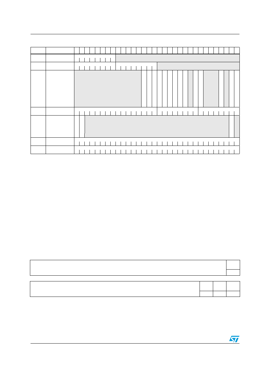
Core peripherals
PM0056
148/154
Doc ID 15491 Rev 3
4.5 SysTick
timer
(STK)
The processor has a 24-bit system timer, SysTick, that counts down from the reload value to
zero, reloads (wraps to) the value in the LOAD register on the next clock edge, then counts
down on subsequent clocks.
When the processor is halted for debugging the counter does not decrement.
4.5.1
SysTick control and status register (STK_CTRL)
Address offset: 0x00
Reset value: 0x0000 0004
Required privilege: Privileged
The SysTick CTRL register enables the SysTick features.
0x1C
SCB_SHPR2
PRI11
Reserved
Reset Value
0
0
0
0
0
0
0
0
0x20
SCB_SHPR3
PRI15
PRI14
Reserved
Reset Value
0
0
0
0
0
0
0
0
0
0
0
0
0
0
0
0
0x24
SCB_SHCRS
Reserved
USG F
A
UL
T ENA
BU
S F
A
U
LT
E
N
A
MEM F
A
UL
T
ENA
SV CALL PE
ND
E
D
B
U
S F
A
UL
T PENDED
ME
M F
A
UL
T
PE
ND
E
D
USG F
A
UL
T PENDED
S
YS TICK
A
C
T
PE
N
D
S
V A
C
T
Re
se
rv
e
d
MONIT
O
R A
C
T
SV CALL A
C
T
Reserved
USG F
A
UL
T A
C
T
Re
se
rv
e
d
BU
S F
A
U
LT
A
C
T
MEM F
A
UL
T
A
C
T
Reset Value
0
0
0
0
0
0
0
0
0
0
0
0
0
0
0x28
SCB_CFSR
UFSR
BFSR
MMFSR
Reset Value
0
0
0
0
0
0
0
0
0
0
0
0
0
0
0
0
0
0
0
0
0
0
0
0
0
0
0
0
0
0
0
0
0x2C
SCB_HFSR
DEB
U
G_VT
FOR
C
ED
Reserved
VECTTBL
Reser
v
ed
Reset Value
0
0
0
0x34
SCB_MMAR
MMAR[31:0]
Reset Value
x
x
x
x
x
x
x
x
x
x
x
x
x
x
x
x
x
x
x
x
x
x
x
x
x
x
x
x
x
x
x
x
0x38
SCB_BFAR
BFAR[31:0]
Reset Value
x
x
x
x
x
x
x
x
x
x
x
x
x
x
x
x
x
x
x
x
x
x
x
x
x
x
x
x
x
x
x
x
Table 47.
SCB register map and reset values (continued)
Offset
Register
31
30
29
28
27
26
25
24
23
22
21
20
19
18
17
16
15
14
13
12
11
10
9
8
7
6
5
4
3
2
1
0
31
30
29
28
27
26
25
24
23
22
21
20
19
18
17
16
Reserved
COUNT
FLAG
rw
15
14
13
12
11
10
9
8
7
6
5
4
3
2
1
0
Reserved
CLKSO
URCE
TICK
INT
EN
ABLE
rw
rw
rw
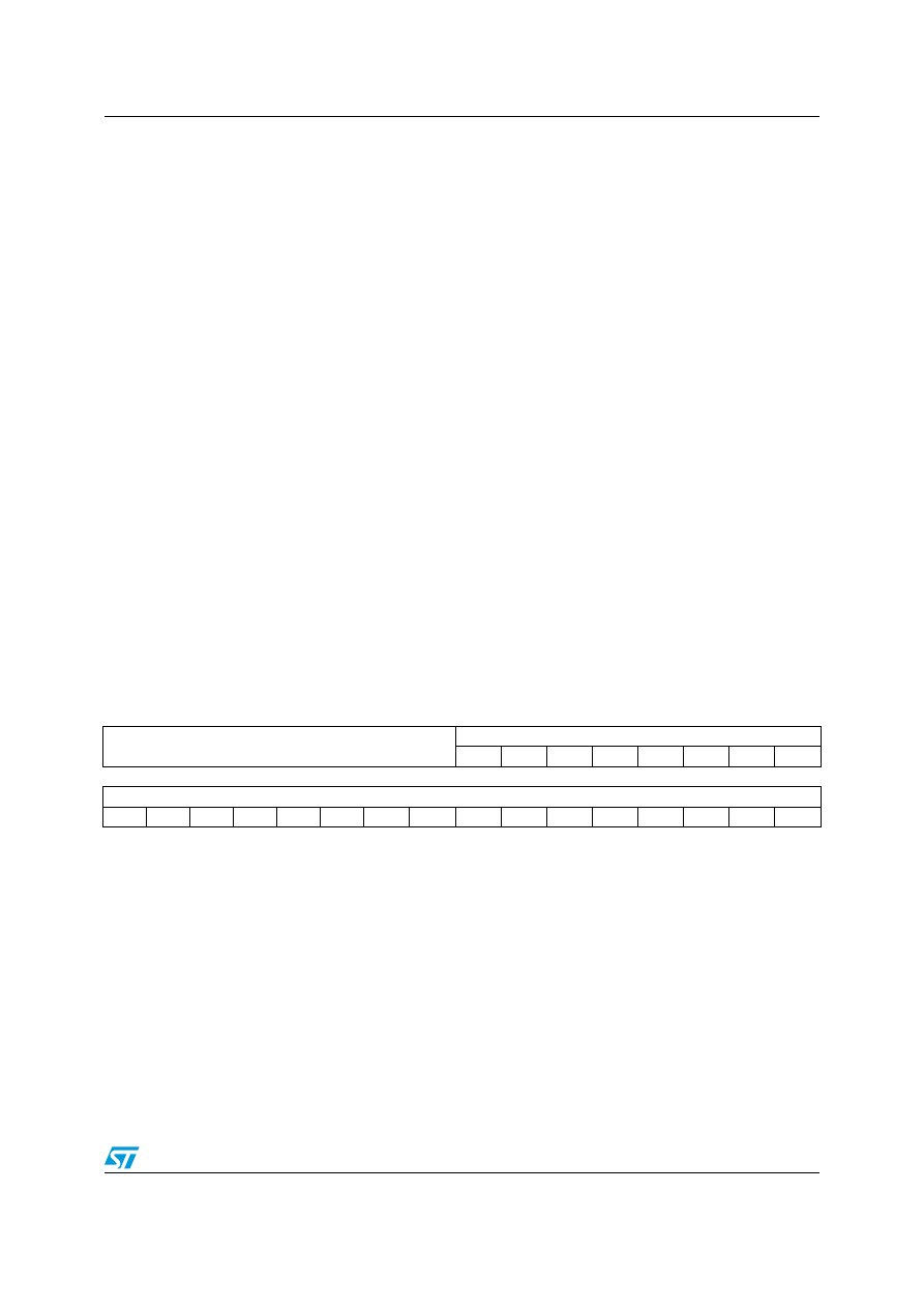
PM0056
Core peripherals
Doc ID 15491 Rev 3
149/154
4.5.2 SysTick
reload
value register (STK_LOAD)
Address offset: 0x04
Reset value: 0x0000 0000
Required privilege: Privileged
Bits 31:17 Reserved, must be kept cleared.
Bit 16 COUNTFLAG:
Returns 1 if timer counted to 0 since last time this was read.
Bits 15:3 Reserved, must be kept cleared.
Bit 2 CLKSOURCE: Clock source selection
Selects the clock source.
0: AHB/8
1: Processor clock (AHB)
Bit 1 TICKINT: SysTick exception request enable
0: Counting down to zero does not assert the SysTick exception request
1: Counting down to zero to asserts the SysTick exception request.
Note: Software can use COUNTFLAG to determine if SysTick has ever counted to zero.
Bit 0 ENABLE: Counter enable
Enables the counter. When ENABLE is set to 1, the counter loads the RELOAD value from the
LOAD register and then counts down. On reaching 0, it sets the COUNTFLAG to 1 and
optionally asserts the SysTick depending on the value of TICKINT. It then loads the RELOAD
value again, and begins counting.
0: Counter disabled
1: Counter enabled
31
30
29
28
27
26
25
24
23
22
21
20
19
18
17
16
Reserved
RELOAD[23:16]
rw
rw
rw
rw
rw
rw
rw
rw
15
14
13
12
11
10
9
8
7
6
5
4
3
2
1
0
RELOAD[15:0]
rw
rw
rw
rw
rw
rw
rw
rw
rw
rw
rw
rw
rw
rw
rw
rw

Core peripherals
PM0056
150/154
Doc ID 15491 Rev 3
Bits 31:24 Reserved, must be kept cleared.
Bits 23:0 RELOAD[23:0]: RELOAD value
The LOAD register specifies the start value to load into the VAL register when the counter is
enabled and when it reaches 0.
Calculating the RELOAD value
The RELOAD value can be any value in the range 0x00000001-0x00FFFFFF. A start value of
0 is possible, but has no effect because the SysTick exception request and COUNTFLAG are
activated when counting from 1 to 0.
The RELOAD value is calculated according to its use:
●
To generate a multi-shot timer with a period of N processor clock cycles, use a RELOAD
value of N-1. For example, if the SysTick interrupt is required every 100 clock pulses, set
RELOAD to 99.
●
To deliver a single SysTick interrupt after a delay of N processor clock cycles, use a
RELOAD of value N. For example, if a SysTick interrupt is required after 400 clock
pulses, set RELOAD to 400.
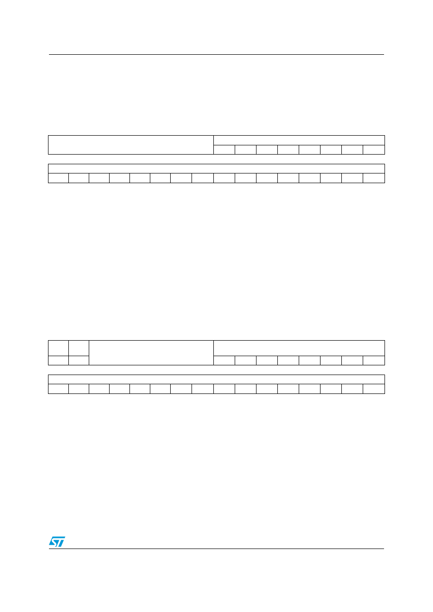
PM0056
Core peripherals
Doc ID 15491 Rev 3
151/154
4.5.3 SysTick
current
value register (STK_VAL)
Address offset: 0x08
Reset value: 0x0000 0000
Required privilege: Privileged
4.5.4 SysTick
calibration
value register (STK_CALIB)
Address offset: 0x0C
Reset value:
0x0002328
Required privilege: Privileged
The CALIB register indicates the SysTick calibration properties.
31
30
29
28
27
26
25
24
23
22
21
20
19
18
17
16
Reserved
CURRENT[23:16]
rw
rw
rw
rw
rw
rw
rw
rw
15
14
13
12
11
10
9
8
7
6
5
4
3
2
1
0
CURRENT[15:0]
rw
rw
rw
rw
rw
rw
rw
rw
rw
rw
rw
rw
rw
rw
rw
rw
Bits 31:24 Reserved, must be kept cleared.
Bits 23:0 CURRENT[23:0]: Current counter value
The VAL register contains the current value of the SysTick counter.
Reads return the current value of the SysTick counter.
A write of any value clears the field to 0, and also clears the COUNTFLAG bit in the
STK_CTRL register to 0.
31
30
29
28
27
26
25
24
23
22
21
20
19
18
17
16
NO
REF
SKEW
Reserved
TENMS[23:16]
r
r
r
r
r
r
r
r
r
r
15
14
13
12
11
10
9
8
7
6
5
4
3
2
1
0
TENMS[15:0]
r
r
r
r
r
r
r
r
r
r
r
r
r
r
r
r
Bit 31 NOREF: NOREF flag
Reads as zero. Indicates that a separate reference clock is provided. The frequency of this
clock is HCLK/8.
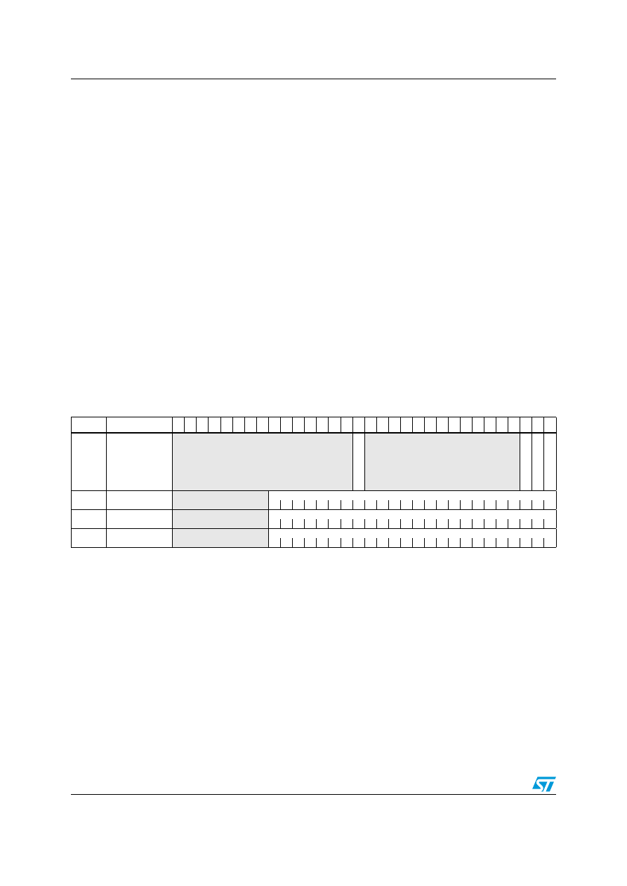
Core peripherals
PM0056
152/154
Doc ID 15491 Rev 3
4.5.5
SysTick design hints and tips
The SysTick counter runs on the processor clock. If this clock signal is stopped for low
power mode, the SysTick counter stops.
Ensure software uses aligned word accesses to access the SysTick registers.
4.5.6
SysTick register map
The table provides shows the SysTick register map and reset values. The base address of
the SysTick register block is 0xE000 E010.
Bit 30 SKEW: SKEW flag
Reads as one. Calibration value for the 1 ms inexact timing is not known because TENMS is
not known. This can affect the suitability of SysTick as a software real time clock.
Bits 29:24 Reserved, must be kept cleared.
Bits 23:0 TENMS[23:0]: Calibration value
Indicates the calibration value when the SysTick counter runs on HCLK max/8 as external
clock. The value is product dependent, please refer to the Product Reference Manual, SysTick
Calibration Value section. When HCLK is programmed at the maximum frequency, the SysTick
period is 1ms.
If calibration information is not known, calculate the calibration value required from the
frequency of the processor clock or external clock.
Table 48.
SysTick register map and reset values
Offset
Register
31
30
29
28
27
26
25
24
23
22
21
20
19
18
17
16
15
14
13
12
11
10
9
8
7
6
5
4
3
2
1
0
0x00
STK_CTRL
Reserved
COUN
TFLA
G
Reserved
CLK
S
OURCE
TI
C
K
IN
T
EN ABL
E
Reset Value
0
1
0
0
0x04
STK_LOAD
Reserved
RELOAD[23:0]
Reset Value
0
0
0
0
0
0
0
0
0
0
0
0
0
0
0
0
0
0
0
0
0
0
0
0
0x08
STK_VAL
Reserved
CURRENT[23:0]
Reset Value
0
0
0
0
0
0
0
0
0
0
0
0
0
0
0
0
0
0
0
0
0
0
0
0
0x0C
STK_CALIB
Reserved
TENMS[23:0]
Reset Value
0
0
0
0
0
0
0
0
0
0
0
0
0
0
0
0
0
0
0
0
0
0
0
0
PM0056
Revision history
Doc ID 15491 Rev 3
153/154
5 Revision
history
Table 49.
Document revision history
Date
Revision
Changes
03-Apr-2009
1
Initial release.
26-Oct-2009
2
modified.
16-Apr-2010
3
Modified
Table 14: Peripheral memory bit-banding regions on
(peripheral bit-band alias and peripheral bit-band region
swapped)
Added
Section 4.2: Memory protection unit (MPU) on page 106
Modified
Table 44: NVIC register map and reset values on page 129
supporting up to 81 interrupts

PM0056
154/154
Doc ID 15491 Rev 3
Please Read Carefully:
Information in this document is provided solely in connection with ST products. STMicroelectronics NV and its subsidiaries (“ST”) reserve the
right to make changes, corrections, modifications or improvements, to this document, and the products and services described herein at any
time, without notice.
All ST products are sold pursuant to ST’s terms and conditions of sale.
Purchasers are solely responsible for the choice, selection and use of the ST products and services described herein, and ST assumes no
liability whatsoever relating to the choice, selection or use of the ST products and services described herein.
No license, express or implied, by estoppel or otherwise, to any intellectual property rights is granted under this document. If any part of this
document refers to any third party products or services it shall not be deemed a license grant by ST for the use of such third party products
or services, or any intellectual property contained therein or considered as a warranty covering the use in any manner whatsoever of such
third party products or services or any intellectual property contained therein.
UNLESS OTHERWISE SET FORTH IN ST’S TERMS AND CONDITIONS OF SALE ST DISCLAIMS ANY EXPRESS OR IMPLIED
WARRANTY WITH RESPECT TO THE USE AND/OR SALE OF ST PRODUCTS INCLUDING WITHOUT LIMITATION IMPLIED
WARRANTIES OF MERCHANTABILITY, FITNESS FOR A PARTICULAR PURPOSE (AND THEIR EQUIVALENTS UNDER THE LAWS
OF ANY JURISDICTION), OR INFRINGEMENT OF ANY PATENT, COPYRIGHT OR OTHER INTELLECTUAL PROPERTY RIGHT.
UNLESS EXPRESSLY APPROVED IN WRITING BY AN AUTHORIZED ST REPRESENTATIVE, ST PRODUCTS ARE NOT
RECOMMENDED, AUTHORIZED OR WARRANTED FOR USE IN MILITARY, AIR CRAFT, SPACE, LIFE SAVING, OR LIFE SUSTAINING
APPLICATIONS, NOR IN PRODUCTS OR SYSTEMS WHERE FAILURE OR MALFUNCTION MAY RESULT IN PERSONAL INJURY,
DEATH, OR SEVERE PROPERTY OR ENVIRONMENTAL DAMAGE. ST PRODUCTS WHICH ARE NOT SPECIFIED AS "AUTOMOTIVE
GRADE" MAY ONLY BE USED IN AUTOMOTIVE APPLICATIONS AT USER’S OWN RISK.
Resale of ST products with provisions different from the statements and/or technical features set forth in this document shall immediately void
any warranty granted by ST for the ST product or service described herein and shall not create or extend in any manner whatsoever, any
liability of ST.
ST and the ST logo are trademarks or registered trademarks of ST in various countries.
Information in this document supersedes and replaces all information previously supplied.
The ST logo is a registered trademark of STMicroelectronics. All other names are the property of their respective owners.
© 2010 STMicroelectronics - All rights reserved
STMicroelectronics group of companies
Australia - Belgium - Brazil - Canada - China - Czech Republic - Finland - France - Germany - Hong Kong - India - Israel - Italy - Japan -
Malaysia - Malta - Morocco - Philippines - Singapore - Spain - Sweden - Switzerland - United Kingdom - United States of America
www.st.com
Document Outline
- 1 About this document
- 2 The Cortex-M3 processor
- 2.1 Programmers model
- 2.1.1 Processor mode and privilege levels for software execution
- 2.1.2 Stacks
- 2.1.3 Core registers
- Figure 2. Processor core registers
- Table 2. Core register set summary (continued)
- Figure 3. APSR, IPSR and EPSR bit assignments
- Figure 4. PSR bit assignments
- Table 3. PSR register combinations
- Table 4. APSR bit definitions
- Table 5. IPSR bit definitions
- Table 6. EPSR bit definitions
- Figure 5. PRIMASK bit assignments
- Table 7. PRIMASK register bit definitions
- Figure 6. FAULTMASK bit assignments
- Table 8. FAULTMASK register bit definitions
- Figure 7. BASEPRI bit assignments
- Table 9. BASEPRI register bit assignments
- Figure 8. CONTROL bit assignments
- Table 10. CONTROL register bit definitions (continued)
- 2.1.4 Exceptions and interrupts
- 2.1.5 Data types
- 2.1.6 The Cortex microcontroller software interface standard (CMSIS)
- 2.2 Memory model
- Figure 9. Memory map
- 2.2.1 Memory regions, types and attributes
- 2.2.2 Memory system ordering of memory accesses
- 2.2.3 Behavior of memory accesses
- 2.2.4 Software ordering of memory accesses
- 2.2.5 Bit-banding
- 2.2.6 Memory endianness
- 2.2.7 Synchronization primitives
- 2.2.8 Programming hints for the synchronization primitives
- 2.3 Exception model
- 2.4 Fault handling
- 2.5 Power management
- 2.1 Programmers model
- 3 The Cortex-M3 instruction set
- 3.1 Instruction set summary
- 3.2 Intrinsic functions
- 3.3 About the instruction descriptions
- 3.4 Memory access instructions
- 3.5 General data processing instructions
- 3.6 Multiply and divide instructions
- 3.7 Saturating instructions
- 3.8 Bitfield instructions
- 3.9 Miscellaneous instructions
- 4 Core peripherals
- 4.1 About the STM32 core peripherals
- 4.2 Memory protection unit (MPU)
- Table 34. Memory attributes summary
- 4.2.1 MPU access permission attributes
- 4.2.2 MPU mismatch
- 4.2.3 Updating an MPU region
- 4.2.4 MPU design hints and tips
- 4.2.5 MPU type register (MPU_TYPER)
- 4.2.6 MPU control register (MPU_CR)
- 4.2.7 MPU region number register (MPU_RNR)
- 4.2.8 MPU region base address register (MPU_RBAR)
- 4.2.9 MPU region attribute and size register (MPU_RASR)
- 4.3 Nested vectored interrupt controller (NVIC)
- 4.3.1 The CMSIS mapping of the Cortex-M3 NVIC registers
- 4.3.2 Interrupt set-enable registers (NVIC_ISERx)
- 4.3.3 Interrupt clear-enable registers (NVIC_ICERx)
- 4.3.4 Interrupt set-pending registers (NVIC_ISPRx)
- 4.3.5 Interrupt clear-pending registers (NVIC_ICPRx)
- 4.3.6 Interrupt active bit registers (NVIC_IABRx)
- 4.3.7 Interrupt priority registers (NVIC_IPRx)
- 4.3.8 Software trigger interrupt register (NVIC_STIR)
- 4.3.9 Level-sensitive and pulse interrupts
- 4.3.10 NVIC design hints and tips
- 4.3.11 NVIC register map
- 4.4 System control block (SCB)
- 4.4.1 CPUID base register (SCB_CPUID)
- 4.4.2 Interrupt control and state register (SCB_ICSR)
- 4.4.3 Vector table offset register (SCB_VTOR)
- 4.4.4 Application interrupt and reset control register (SCB_AIRCR)
- 4.4.5 System control register (SCB_SCR)
- 4.4.6 Configuration and control register (SCB_CCR)
- 4.4.7 System handler priority registers (SHPRx)
- 4.4.8 System handler control and state register (SCB_SHCSR)
- 4.4.9 Configurable fault status register (SCB_CFSR)
- 4.4.10 Hard fault status register (SCB_HFSR)
- 4.4.11 Memory management fault address register (SCB_MMFAR)
- 4.4.12 Bus fault address register (SCB_BFAR)
- 4.4.13 System control block design hints and tips
- 4.4.14 SCB register map
- 4.5 SysTick timer (STK)
- 5 Revision history
Wyszukiwarka
Podobne podstrony:
CARPROG BMW Key programmer manual
CARPROG Motorola HC12 programmer manual
CARPROG MB key programmer manual
CARPROG Motorola HC05 programmer manual
KG 659E Updated version Programming manual
Genicom 5000 Programmer's Manual
fanuc cnc program manual gcode
Cortex M3 User Guide
CARPROG Motorola HC08 programmer manual
CARPROG Motorola HC11 programmer manual
CARPROG BMW Key programmer manual
DoD Nuclear Weapon System Safety Program Manual
Sole Control Sc230 Sc240 Sc241 Remote Programming Manual
więcej podobnych podstron