REV. 0
Information furnished by Analog Devices is believed to be accurate and
reliable. However, no responsibility is assumed by Analog Devices for its
use, nor for any infringements of patents or other rights of third parties
which may result from its use. No license is granted by implication or
otherwise under any patent or patent rights of Analog Devices.
a
AD8314
One Technology Way, P.O. Box 9106, Norwood, MA 02062-9106, U.S.A.
Tel: 781/329-4700
World Wide Web Site: http://www.analog.com
Fax: 781/326-8703
© Analog Devices, Inc., 1999
100 MHz–2500 MHz 45 dB
RF Detector/Controller
FEATURES
Complete RF Detector/Controller Function
Typical Range –58 dBV to –13 dBV
–45 dBm to 0 dBm re 50
⍀
Frequency Response from 100 MHz to 2.5 GHz
Temperature-Stable Linear-in-dB Response
Accurate to 2.5 GHz
Rapid Response: 70 ns to a 10 dB Step
Low Power: 12 mW at 2.7 V
Power-Down to 20
A
APPLICATIONS
Cellular Handsets (TDMA, CDMA, GSM)
RSSI and TSSI for Wireless Terminal Devices
Transmitter Power Measurement and Control
PRODUCT DESCRIPTION
The AD8314 is a complete low-cost subsystem for the mea-
surement and control of RF signals in the frequency range
0.1 GHz–2.5 GHz, with a typical dynamic range of 45 dB,
intended for use in a wide variety of cellular handsets and other
wireless devices. It provides a wider dynamic range and better
accuracy than possible using discrete diode detectors. In particular,
its temperature stability is excellent over the full operating range of
–30
°
C to +85
°
C.
Its high sensitivity allows control at low power levels, thus
reducing the amount of power that needs to be coupled to the
detector. It is essentially a voltage-responding device, with a
typical signal range of 1.25 mV to 224 mV rms or –58 dBV to
–13 dBV. This is equivalent to –45 dBm to 0 dBm re 50
Ω
.
For convenience, the signal is internally ac-coupled, using a 5 pF
capacitor to a load of 3 k
Ω
in shunt with 2 pF. This high-pass
coupling, with a corner at 16 MHz, determines the lowest oper-
ating frequency. Thus, the source may be dc-grounded.
The AD8314 provides two voltage outputs. The first, called
V_UP, increases from close to ground to about 1.2 V as the
input signal level increases from 1.25 mV to 224 mV. This output
is intended for use in measurement mode. Consult the Appli-
cations section of this data sheet for information on use in this
mode. A capacitor may be connected between the V_UP and
FLTR pins when it is desirable to increase the time interval over
which averaging of the input waveform occurs.
The second output, V_DN, is an inversion of V_UP, but with
twice the slope and offset by a fixed amount. This output starts
at about 2.25 V (provided the supply voltage is
≥
3.3 V) for
the minimum input and falls to a value close to ground at the
maximum input. This output is intended for analog control
loop applications. A setpoint voltage is applied to VSET and
V_DN is then used to control a VGA or power amplifier. Here
again, an external filter capacitor may be added to extend the
averaging time. Consult the Applications section of this data
sheet for information on use in this mode.
The AD8314 is available in a micro_SOIC package and con-
sumes 4.5 mA from a 2.7 V to 5.5 V supply. When powered
down, the typical sleep current is 20
µ
A.
FUNCTIONAL BLOCK DIAGRAM
10dB
OFFSET
COMP'N
V-I
I-V
RFIN
COMM
(PADDLE)
VPOS
X2
ENBL
V DN
V UP
VSET
FLTR
AD8314
10dB
10dB
10dB
BAND-GAP
REFERENCE
DET
DET
DET
DET
DET

–2–
REV. 0
AD8314–SPECIFICATIONS
(V
S
= 3 V, T
A
= +25
ⴗC, unless otherwise noted)
Parameter
Condition
Min
Typ
Max
Unit
OVERALL FUNCTION
Frequency Range
To Meet All Specifications
0.1
2.5
GHz
Input Voltage Range
Internally AC-Coupled
1.25
224
mV rms
Equivalent Power Range
52.3
Ω
External Termination
–45
0
dBm
Logarithmic Slope
Main Output, V_UP, 100 MHz
1
18.85
21.3
23.35
mV/dB
Logarithmic Intercept
Main Output, V_UP, 100 MHz
–68
–62
–56
dBV
Equivalent dBm Level
52.3
Ω
External Termination
–55
–49
–43
dBm
INPUT INTERFACE
(Pin RFIN)
DC Resistance to COMM
100
k
Ω
Inband Input Resistance
f = 0.1 GHz
3
k
Ω
Input Capacitance
f = 0.1 GHz
2
pF
MAIN OUTPUT
(Pin V_UP)
Voltage Range
V_UP Connected to VSET
0.01
1.2
V
Minimum Output Voltage
No Signal at RFIN, R
L
≥
10 k
Ω
0.01
0.02
0.05
V
Maximum Output Voltage
2
R
L
≥
10 k
Ω
1.9
2
V
General Limit
2.7 V
≤
V
S
≤
5.5 V
V
S
– 1.1
V
S
– 1
V
Available Output Current
Sourcing/Sinking
1/0.5
2/1
mA
Response Time
10%–90%, 10 dB Step
70
ns
Residual RF (at 2f)
f = 0.1 GHz (Worst Condition)
100
µ
V
INVERTED OUTPUT
(Pin V_DN)
Gain Referred to V_UP
V
DN
= 2.25 V – 2
×
V
UP
–2
Minimum Output Voltage
V
S
≥
3.3 V
0.01
0.05
0.1
V
Maximum Output Voltage
V
S
≥
3.3 V
3
2.1
2.2
2.5
V
Available Output Current
Sourcing/Sinking
4/100
6/200
mA/
µ
A
Output-Referred Noise
RF Input = 2 GHz, –33 dBV, f
NOISE
= 10 kHz
1.05
µ
V/
√
Hz
Response Time
10%–90%, 10 dB Input Step
70
ns
Full-Scale Settling Time
–40 dBm to 0 dBm Input Step, to 95%
150
ns
SETPOINT INPUT
(Pin VSET)
Voltage Range
Corresponding to Central 40 dB
0.15
1.2
V
Input Resistance
7
10
k
Ω
Logarithmic Scale Factor
f = 0.900 GHz
20.7
mV/dB
f = 1.900 GHz
19.7
mV/dB
ENABLE INTERFACE
(Pin ENBL)
Logic Level to Enable Power
HI Condition, –30
°
C
≤
T
A
≤
+85
°
C
1.6
V
POS
V
Input Current when HI
2.7 V at ENBL, –30
°
C
≤
T
A
≤
+85
°
C
20
300
µ
A
Logic Level to Disable Power
LO Condition, –30
°
C
≤
T
A
≤
+85
°
C
–0.5
0.8
V
POWER INTERFACE
(Pin VPOS)
Supply Voltage
2.7
3.0
5.5
V
Quiescent Current
3.0
4.5
5.7
mA
Over Temperature
–30
°
C
≤
T
A
≤
+85
°
C
2.7
4.4
6.6
mA
Total Supply Current when Disabled
20
95
µ
A
Over Temperature
–30
°
C
≤
T
A
≤
+85
°
C
40
µ
A
NOTES
1
Mean and Standard Deviation specifications are available in Table I.
2
Increased output possible when using an attenuator between V_UP and VSET to raise the slope.
3
Refer to Figure 19 for details.
Specifications subject to change without notice.
AD8314
–3–
REV. 0
ABSOLUTE MAXIMUM RATINGS
*
Supply Voltage VPOS . . . . . . . . . . . . . . . . . . . . . . . . . . .5.5 V
V_UP, V_DN, VSET, ENBL . . . . . . . . . . . . . . . . 0 V, VPOS
Input Voltage . . . . . . . . . . . . . . . . . . . . . . . . . . . . . . 1.6 V rms
Equivalent Power . . . . . . . . . . . . . . . . . . . . . . . . . . . +17 dBm
Internal Power Dissipation . . . . . . . . . . . . . . . . . . . . 200 mW
θ
JA
. . . . . . . . . . . . . . . . . . . . . . . . . . . . . . . . . . . . . . . . . 200
°
C
Maximum Junction Temperature . . . . . . . . . . . . . . . . . 125
°
C
Operating Temperature Range . . . . . . . . . . . –30
°
C to +85
°
C
Storage Temperature Range . . . . . . . . . . . . –65
°
C to +150
°
C
Lead Temperature Range (Soldering 60 sec) . . . . . . . . . 300
°
C
*Stresses above those listed under Absolute Maximum Ratings may cause permanent
damage to the device. This is a stress rating only; functional operation of the device
at these or any other conditions above those indicated in the operational section
of this specification is not implied. Exposure to absolute maximum rating conditions
for extended periods may affect device reliability.
CAUTION
ESD (electrostatic discharge) sensitive device. Electrostatic charges as high as 4000 V readily
accumulate on the human body and test equipment and can discharge without detection. Although
the AD8314 features proprietary ESD protection circuitry, permanent damage may occur on
devices subjected to high energy electrostatic discharges. Therefore, proper ESD precautions are
recommended to avoid performance degradation or loss of functionality.
WARNING!
ESD SENSITIVE DEVICE
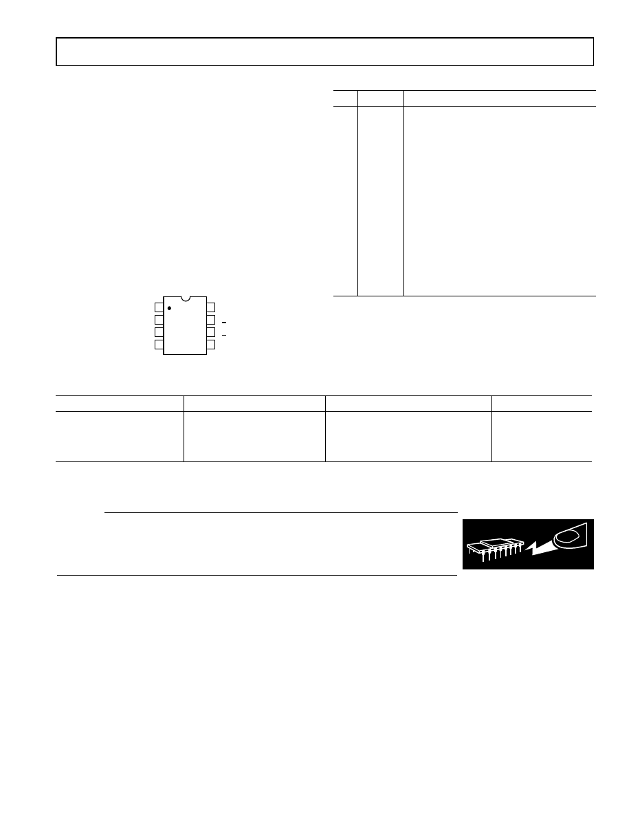
Pin Function Descriptions
Pin
Name
Function
1
RFIN
RF Input.
2
ENBL
Connect pin to V
S
for normal operation.
Connect pin to ground for disable mode.
3
VSET
Setpoint input for operation in controller
mode. To operate in detector mode connect
VSET to V_UP
4
FLTR
Connection for an external capacitor to slow
the response of the output. Capacitor is con-
nected between FLTR and V_UP.
5
COMM
Device Common (Ground).
6
V_UP
Logarithmic output. Output voltage increases
with increasing input amplitude.
7
V_DN
Inversion of V_UP, governed by the following
equation: V_DN = 2.25 V – 2
×
V
UP
.
8
VPOS
Positive supply voltage (V
S
), 2.7 V to 5.5 V.
PIN CONFIGURATION
TOP VIEW
(Not to Scale)
8
7
6
5
1
2
3
4
RFIN
ENBL
VSET
VPOS
V DN
V UP
COMM
FLTR
AD8314
ORDERING GUIDE
Model
Temperature Range
Package Description
Package Option
AD8314ARM
*
–30
°
C to +85
°
C
Tube, 8-Lead micro_SOIC
RM-8
AD8314ARM-REEL
13" Tape and Reel
AD8314ARM-REEL7
7" Tape and Reel
AD8314-EVAL
Evaluation Board
*Device branded as J5A.
AD8314
–4–
REV. 0
INPUT AMPLITUDE – dBV
1.2
0
–75
–5
–65
V
UP
– Volts
–55
–45
–35
–25
–15
1.0
0.8
0.6
0.4
0.2
(–52dBm)
(–2dBm)
2.5GHz
1.9GHz
0.9GHz
0.1GHz
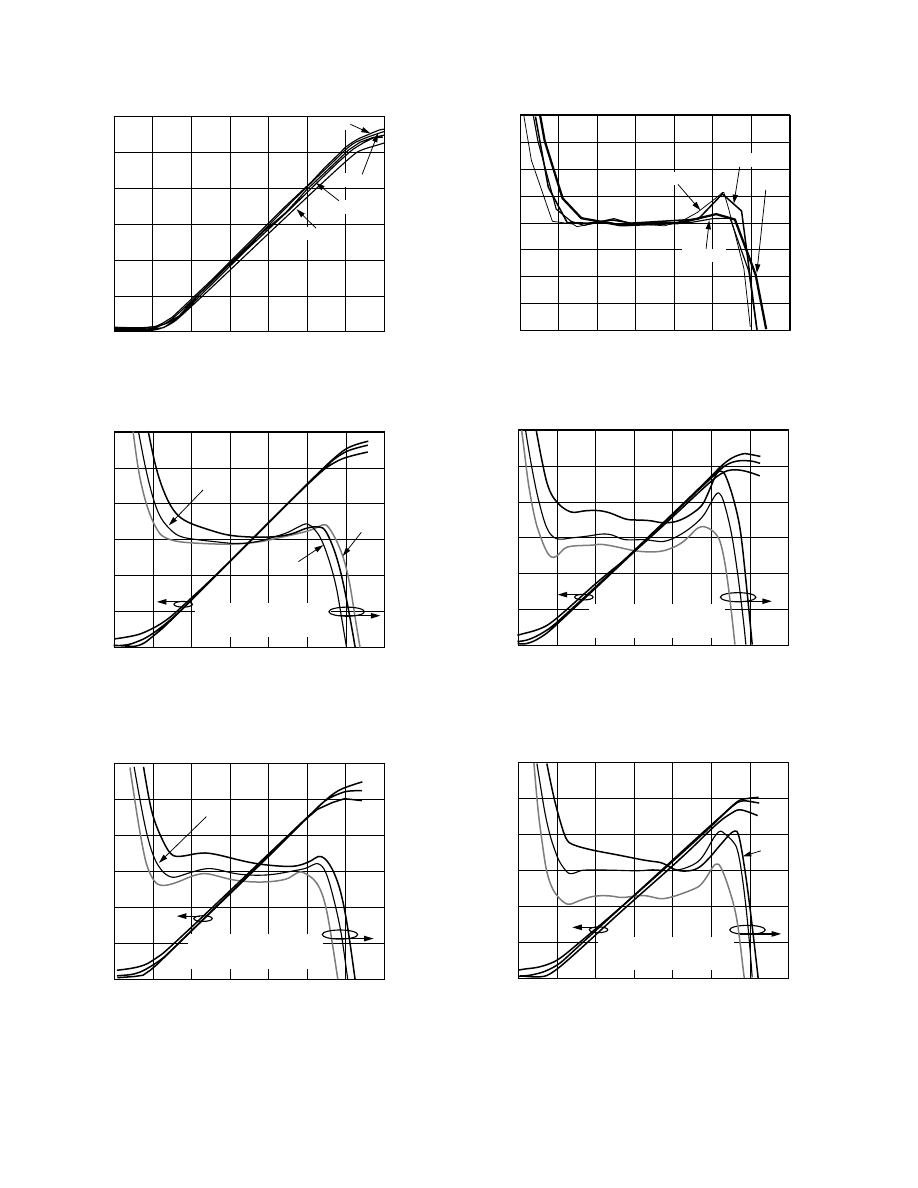
Figure 1. V
UP
vs. Input Amplitude
INPUT AMPLITUDE – dBV
1.2
0
–70
0
–60
(–47dBm)
V
UP
– Volts
–50
–40
–30
–20
–10
(+3dBm)
1.0
0.8
0.6
0.4
0.2
–30
8
C
+85
8
C
+25
8
C
+25
8
C
–30
8
C
3
–3
2
1
0
–1
–2
SLOPE AND INTERCEPT
NORMALIZED AT +25
8
C AND
APPLIED TO –30
8
C AND +85
8
C
ERROR – dB
Figure 2. V
UP
and Log Conformance vs. Input Amplitude at
0.1 GHz; –30
°
C, +25
°
C, and +85
°
C
INPUT AMPLITUDE – dBV
1.2
0
–70
0
–60
(–47dBm)
V
UP
– Volts
–50
–40
–30
–20
–10
(+3dBm)
1.0
0.8
0.6
0.4
0.2
–30
8
C
+85
8
C
+25
8
C
3
–3
2
1
0
–1
–2
SLOPE AND INTERCEPT
NORMALIZED AT +25
8
C AND
APPLIED TO –30
8
C AND +85
8
C
ERROR – dB
Figure 3. V
UP
and Log Conformance vs. Input Amplitude
at 0.9 GHz; –30
°
C, +25
°
C, and +85
°
C
–Typical Performance Characteristics
INPUT AMPLITUDE – dBV
4
–4
–70
0
–60
ERROR – dB
–50
–40
–30
–20
–10
1
0
–1
–2
–3
2.5GHz
1.9GHz
0.9GHz
(–47dBm)
(+3dBm)
0.1GHz
2
3
Figure 4. Log Conformance vs. Input Amplitude
INPUT AMPLITUDE – dBV
1.2
0
–70
0
–60
(–47dBm)
V
UP
– Volts
–50
–40
–30
–20
–10
(+3dBm)
1.0
0.8
0.6
0.4
0.2
–30
8
C
+85
8
C
+25
8
C
3
–3
2
1
0
–1
–2
SLOPE AND INTERCEPT
NORMALIZED AT +25
8
C AND
APPLIED TO –30
8
C AND +85
8
C
ERROR – dB
Figure 5. V
UP
and Log Conformance vs. Input Amplitude
at 1.9 GHz; –30
°
C, +25
°
C, and +85
°
C
INPUT AMPLITUDE – dBV
1.2
0
–70
0
–60
(–47dBm)
V
UP
– Volts
–50
–40
–30
–20
–10
(+3dBm)
1.0
0.8
0.6
0.4
0.2
–30
8
C
+85
8
C
+25
8
C
3
–3
2
1
0
–1
–2
SLOPE AND INTERCEPT
NORMALIZED AT +25
8
C AND
APPLIED TO –30
8
C AND +85
8
C
ERROR – dB
+85
8
C
Figure 6. V
UP
and Log Conformance vs. Input Amplitude
at 2.5 GHz; –30
°
C, +25
°
C, and +85
°
C
AD8314
–5–
REV. 0
FREQUENCY – GHz
0
0.5
SLOPE – mV/dB
1.0
22
21
20
19
18
–30
8
C
+85
8
C
+25
8
C
1.5
2.0
2.5
23
Figure 7. Slope vs. Frequency; –30
°
C, +25
°
C, and +85
°
C
V
S
– Volts
22
19
2.5
V
UP
SLOPE – mV/dB
21
20
2.5GHz
1.9GHz
0.9GHz
0.1GHz
3.0
3.5
4.0
4.5
5.0
5.5
Figure 8. V
UP
Slope vs. Supply Voltage
FREQUENCY – GHz
0
0.5
1.0
0
1.5
2.0
2.5
500
1000
1500
2000
2500
3000
3500
RESISTANCE –
V
–200
0
–400
–600
–800
–1000
–1200
–1400
X
R
|| - jX
V
|| - j748
V
|| - j106
V
|| - j80
V
|| - j141
V
R
3030
760
301
90
FREQUENCY (GHz)
0.1
0.9
1.9
2.5
R
X
REACTANCE –
V
Figure 9. Input Impedance
FREQUENCY – GHz
0
0.5
1.0
–75
–30
8
C
+85
8
C
+25
8
C
1.5
2.0
2.5
–70
–65
–60
–55
V
UP
INTERCEPT – dBV
Figure 10. V
UP
Intercept vs. Frequency: –30
°
C, +25
°
C, and
+85
°
C
V
S
– Volts
–67
2.5
V
UP
INTERCEPT – dBV
2.5GHz
1.9GHz
0.9GHz
0.1GHz
3.0
3.5
4.0
4.5
5.0
5.5
–66
–65
–64
–63
–62
–61
Figure 11. V
UP
Intercept vs. Supply Voltage
V
ENBL
– Volts
–1
0.2
SUPPLY CURRENT – mA
INCREASING
V
ENBL
0
1
2
3
4
5
6
0.4
0.6
0.8
1.0
1.2
1.4
1.6
1.8
2.0
2.2 2.4
2.6
DECREASING
V
ENBL
Figure 12. Supply Current vs. ENBL Voltage, V
S
= 3 V
AD8314
–6–
REV. 0
1
m
s PER
HORIZONTAL
DIVISION
V
DN
V
UP
V
ENBL
5V PER VERTICAL DIVISION
V
DN
GND
V
UP
GND
V
ENBL
GND
500mV/VERT. DIV.
500mV/VERT. DIV.
AVERAGE: 128 SAMPLES
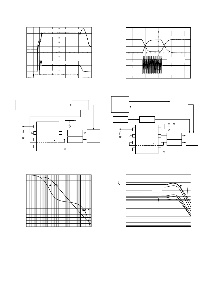
Figure 13. ENBL Response Time
1
2
3
4
ENBL
RFIN
AD8314
RF OUT
TEK
TDS784C
SCOPE
TRIG
OUT
HP8116A
PULSE
GENERATOR
10MHz REF OUTPUT
EXT TRIG
NC = NO CONNECT
0.1
m
F
NC
8
7
6
5
VSET
FLTR
V DN
VPOS
COMM
V UP
TEK P6204
FET PROBE
TEK P6204
FET PROBE
3.0V
PULSE OUT
TRIG
52.3
V
–33dBV
HP8648B
SIGNAL
GENERATOR
Figure 14. Test Setup for ENBL Response Time
FREQUENCY – Hz
80
10
AMPLITUDE – dB
0
PHASE – De
g
rees
75
–10
70
–20
65
–30
60
–40
55
–50
50
–60
45
–70
40
–80
35
–90
30
–100
25
–110
20
–120
15
–130
10
–140
5
–150
0
–160
–5
–170
100
1k
10k
100k
1M
10M
Figure 15. AC Response from VSET to V_DN
200mV PER
VERTICAL
DIVISION
100ns PER
HORIZONTAL
DIVISION
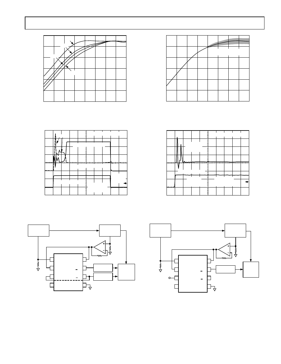
RF INPUT
AVERAGE: 128 SAMPLES
PULSED RF
0.1GHz, –13dBV
GND
GND
V
UP
500mV/
VERT. DIV.
1V/VERT. DIV.
V
DN
Figure 16. V
UP
and V
DN
Response Time, –40 dBm to 0 dBm
1
2
3
4
ENBL
RFIN
AD8314
RF OUT
TEK
TDS784C
SCOPE
TRIG
OUT
PICOSECOND
PULSE LABS
PULSE
GENERATOR
HP8648B
SIGNAL
GENERATOR
PULSE
MODULATION
MODE
10MHz REF OUTPUT
EXT TRIG
NC = NO CONNECT
0.1
m
F
NC
8
7
6
5
VSET
FLTR
V DN
VPOS
COMM
V UP
TEK P6204
FET PROBE
TEK P6204
FET PROBE
3.0V
TRIG
52.3
V
OUT
PULSE MODE IN
–3dB
3.0V
RF
SPLITTER
TEK P6204
FET PROBE
–3dB
Figure 17. Test Setup for Pulse Response
NOISE SPECTRAL DENSITY –
m
V/ Hz
FREQUENCY – Hz
10.0
0.1
100
1.0
1k
10k
100k
1M
10M
–60dBm
–40dBm
–30dBm
–20dBm
RF INPUT
–70dBm
–50dBm
Figure 18. V
DN
Noise Spectral Density
AD8314
–7–
REV. 0
V
S
– Volts
2.3
1.7
2.7
V
DN
– V
2.2
2.1
2.0
1.9
1.8
2.8
2.9
3.0
3.1
3.2
3.3
3.4
3.5
0mA
2mA
4mA
6mA
Figure 19. Maximum V
DN
Voltage vs. V
S
by Load Current
1
m
s PER
HORIZONTAL
DIVISION
VPOS AND ENABLE
2V PER
VERTICAL
DIVISION
V
DN
500mV/VERT. DIV.
V
UP
V
UP
500mV/VERT. DIV.
AVERAGE: 128 SAMPLES
V
DN
GND
V
UP
GND
GND
Figure 20. Power-On and -Off Response, Measurement
Mode
HP8648B
SIGNAL
GENERATOR
1
2
3
4
ENBL
RFIN
AD8314
RF OUT
TEK
TDS784C
SCOPE
TRIG
OUT
HP8116A
PULSE
GENERATOR
10MHz REF OUTPUT
EXT TRIG
NC = NO CONNECT
NC
8
7
6
5
VSET
FLTR
V DN
VPOS
COMM
V UP
TEK P6204
FET PROBE
TEK P6204
FET PROBE
TRIG
52.3
V
PULSE
OUT
49.9
V
AD811
732
V
–33dBV
Figure 21. Test Setup for Power-On and -Off Response
V
S
– Volts
2.3
1.7
2.7
V
DN
– V
2.2
2.1
2.0
1.9
1.8
2.8
2.9
3.0
3.1
3.2
3.3
3.4
3.5
SHADING INDICATES
6
3 SIGMA
Figure 22. Maximum V
DN
Voltage vs. V
S
with 3 mA Load
100ns PER
HORIZONTAL
DIVISION
200mV PER
VERTICAL
DIVISION
V
DN
AVERAGE: 128 SAMPLES
2V PER
VERTICAL
DIVISION
VPOS AND ENABLE
V
DN
GND
GND
Figure 23. Power-On Response, V
DN
, Controller Mode with
VSET Held Low
1
2
3
4
ENBL
RFIN
AD8314
RF OUT
TEK
TDS784C
SCOPE
TRIG
OUT
HP8112A
PULSE
GENERATOR
10MHz REF OUTPUT
EXT TRIG
NC = NO CONNECT
NC
8
7
6
5
VSET
FLTR
V DN
VPOS
COMM
V UP
TEK P6204
FET PROBE
TRIG
52.3
V
+0.2
NC
AD811
PULSE
OUT
49.9
V
732
V
HP8648B
SIGNAL
GENERATOR
Figure 24. Test Setup for Power-On Response at V_DN
Output, Controller Mode with VSET Pin Held Low
AD8314
–8–
REV. 0
Table I. Typical Specifications at Selected Frequencies at 25
ⴗC (Mean and Sigma)
ⴞ1 dB Dynamic Range* – dBV
Slope – mV/dB
Intercept – dBV
High Point
Low Point
Frequency – GHz
0.1
21.3
0.4
–62.2
0.4
–11.8
0.3
–59
0.5
0.9
20.7
0.4
–63.6
0.4
–13.8
0.3
–61.4
0.4
1.9
19.7
0.4
–66.3
0.4
–19
0.7
–64
0.6
2.5
19.2
0.4
–62.1
0.7
–16.4
1.7
–61
1.3
*Refer to Figure 29.
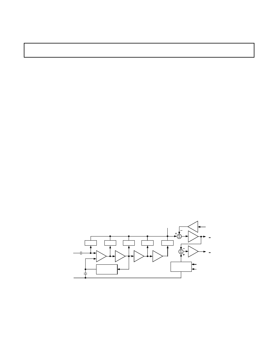
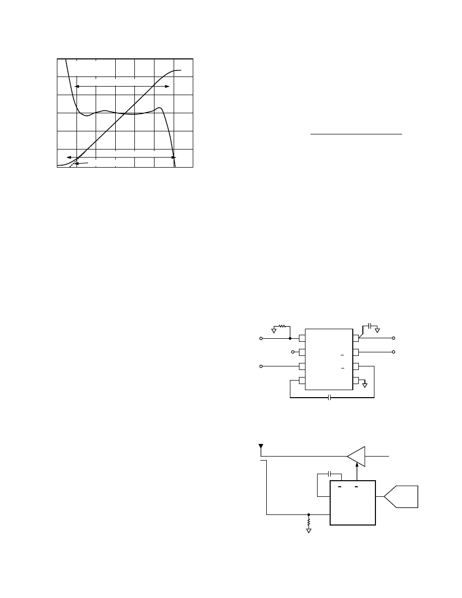
GENERAL DESCRIPTION
The AD8314 is a logarithmic amplifier (log amp) similar in
design to the AD8313; further details about the structure and
function may be found in the AD8313 data sheet and other log
amps produced by Analog Devices. Figure 25 shows the main
features of the AD8314 in block schematic form.
The AD8314 combines two key functions needed for the mea-
surement of signal level over a moderately wide dynamic range.
First, it provides the amplification needed to respond to small
signals, in a chain of four amplifier/limiter cells, each having
a small-signal gain of 10 dB and a bandwidth of approximately
3.5 GHz. At the output of each of these amplifier stages is a
full-wave rectifier, essentially a square-law detector cell, that
converts the RF signal voltages to a fluctuating current having
an average value that increases with signal level. A further passive
detector stage is added ahead of the first stage. Thus, there are
five detectors, each separated by 10 dB, spanning some 50 dB
of dynamic range. The overall accuracy at the extremes of this
total range, viewed as the deviation from an ideal logarithmic
response, that is, the law-conformance error, can be judged by
reference to Figure 4, which shows that errors across the central
40 dB are moderate. Other curves show how the conformance
to an ideal logarithmic function varies with supply voltage,
temperature and frequency.
The output of these detector cells is in the form of a differential
current, making their summation a simple matter. It can easily
be shown that such summation closely approximates a logarith-
mic function. This result is then converted to a voltage, at pin
V_UP, through a high-gain stage. In measurement modes, this
output is connected back to a voltage-to-current (V–I) stage, in
such a manner that V_UP is a logarithmic measure of the RF input
voltage, with a slope and intercept controlled by the design. For
a fixed termination resistance at the input of the AD8314, a given
voltage corresponds to a certain power level.
10dB
OFFSET
COMP'N
V-I
I-V
RFIN
COMM
(PADDLE)
VPOS
X2
ENBL
V DN
V UP
VSET
FLTR
AD8314
10dB
10dB
10dB
BAND-GAP
REFERENCE
DET
DET
DET
DET
DET
Figure 25. Block Schematic
However, in using this part, it must be understood that log amps
do not fundamentally respond to power. It is for this reason that
we use dBV (decibels above 1 V rms) rather than the commonly
used metric of dBm. While the dBV scaling is fixed, independent
of termination impedance, the corresponding power level is not.
For example, 224 mV rms is always –13 dBV (with one further
condition of an assumed sinusoidal waveform; see the Applications
section for more information about the effect of waveform on
logarithmic intercept), and it corresponds to a power of 0 dBm
when the net impedance at the input is 50
Ω
. When this imped-
ance is altered to 200
Ω
, the same voltage clearly represents a
power level that is four times smaller (P = V
2
/R), that is, –6 dBm.
Note that dBV may be converted to dBm for the special case of a
50
Ω
system by simply adding 13 dB (0 dBV is equivalent to
+13 dBm).
Thus, the external termination added ahead of the AD8314
determines the effective power scaling. This will often take the
form of a simple resistor (52.3
Ω
will provide a net 50
Ω
input)
but more elaborate matching networks may be used. This im-
pedance determines the logarithmic intercept, the input power
for which the output would cross the baseline (V_UP = zero) if
the function were continuous for all values of input. Since this is
never the case for a practical log amp, the intercept refers to
the value obtained by the minimum-error straight-line fit to the
actual graph of V_UP versus P
IN
(more generally, V
IN
). Again,
keep in mind that the quoted values assume a sinusoidal (CW)
signal. Where there is complex modulation, as in CDMA, the
calibration of the power response needs to be adjusted accordingly.
Where a true power (waveform-independent) response is needed,
the use of an rms-responding detector, such as the AD8361,
should be considered.
However, the logarithmic slope, the amount by which the output
V_UP changes for each decibel of input change (voltage or
power) is, in principle, independent of waveform or termination
impedance. In practice, it usually falls off somewhat at higher
AD8314
–9–
REV. 0
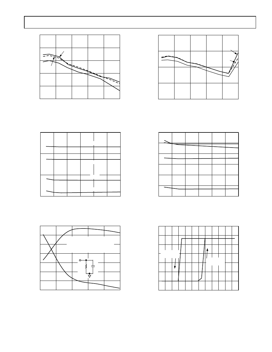
frequencies, due to the declining gain of the amplifier stages and
other effects in the detector cells. For the AD8314, the slope
at low frequencies is nominally 21.3 mV/dB, falling almost linearly
with frequency to about 19.2 mV/dB at 2.5 GHz. These values
are sensibly independent of temperature (see Figure 7) and
almost totally unaffected by the supply voltage from 2.7 V to
5.5 V (Figure 8).
Inverted Output
The second provision is the inclusion of an inverting amplifier
to the output, for use in controller applications. Most power
amplifiers require a gain-control bias that must decrease from a
large positive value toward ground level as the power output is
required to decrease. This control voltage, which appears at the pin
V_DN, is not only of the opposite polarity to V_UP, but also
needs to have an offset added in order to determine its most posi-
tive value when the power level (assumed to be monitored through
a directional coupler at the output of the PA) is minimal.
The starting value of V_DN is nominally 2.25 V, and it falls
on a slope of twice that of V_UP, in other words, –43 mV/dB.
Figure 26 shows how this is achieved: the reference voltage
that determines the maximum output is derived from the on-
chip voltage reference, and is substantially independent of the
supply voltage or temperature. However, the full output cannot
be attained for supply voltages under 3.3 V; Figure 19 shows
this dependency. The relationship between V_UP and V_DN is
shown in Figure 27.
V–I
BAND-GAP
REFERENCE
+2
VSET
FLTR
I–V
1.125V
V
DN
= 2.25V – 2.0
3
V_UP
CURRENTS FROM
DETECTORS
AD8314
V_UP
V_DN
Figure 26. Output Interfaces
INPUT AMPLITUDE – dBV
0
–60
VOLTS
2.5
2.0
1.5
1.0
0.5
OUTPUT FOR
PA CONTROL
–50
–40
–30
–20
–10
0
OUTPUT FOR
MEASUREMENT
V_UP
V_DN
Figure 27. Showing V_UP and V_DN Relationship
APPLICATIONS
Basic Connections
Figure 28 shows connections for the basic measurement mode.
A supply voltage of 2.7 V to 5.5 V is required. The supply to
the VPOS pin should be decoupled with a low inductance 0.1
µ
F
surface mount ceramic capacitor. A series resistor of about 10
Ω
may be added; this resistor will slightly reduce the supply voltage to
the AD8314 (maximum current into the VPOS pin is approxi-
mately 9 mA when V_DN is delivering 5 mA). Its use should be
avoided in applications where the power supply voltage is very
low (i.e., 2.7 V). A series inductor will provide similar power
supply filtering with minimal drop in supply voltage.
1
2
3
4
ENBL
RFIN
AD8314
8
7
6
5
VSET
FLTR
V DN
VPOS
COMM
V UP
0.1
m
F
OPTIONAL
(SEE TEXT)
OPTIONAL
(SEE TEXT)
V
S
V
DN
V
UP
C
F
V
S
52.3
V
INPUT
Figure 28. Basic Connections for Operation in
Measurement Mode
The ENBL pin is here connected to VPOS. The AD8313 may
be disabled by pulling this pin to ground when the chip current
is reduced to about 20
µ
A from its normal value of 4.5 mA.
The logic threshold is around +V
S
/2 and the enable function
occurs in about 1.5
µ
s. Note, however, further settling time is
generally needed at low input levels.
The AD8314 has an internal input coupling capacitor. This
eliminates the need for external ac-coupling. A broadband input
match is achieved in this example by connecting a 52.3
Ω
resis-
tor between RFIN and ground. This resistance combines with
the internal input impedance of approximately 3 k
Ω
to give
an overall broadband input resistance of 50
Ω
. Several other
coupling methods are possible; these are described in the Input
Coupling section.
The measurement mode is selected by connecting VSET to V_UP,
which establishes a feedback path and sets the logarithmic slope
to its nominal value. The peak voltage range of the measurement
extends from –58 dBV to –13 dBV at 0.9 GHz, and only slightly
less at higher frequencies up to 2.5 GHz. Thus, using the 50
Ω
termination, the equivalent power range is –45 dBm to 0 dBm.
At a slope of 21.5 mV/dB, this would amount to an output span
of 967 mV. Figure 29 shows the transfer function for V_UP at a
supply voltage of 3 V, and input frequency of 0.9 GHz.
V_DN, which will generally not be used when the AD8314 is
used in the measurement mode, is essentially an inverted version
of V_UP. The voltage on V_UP and V_DN are related by the
equation.
V
DN
= 2.25 V – 2 V
UP
While V_DN can deliver up to 6 mA, the load resistance on V_UP
should not be lower than 10 k
Ω
in order that the full-scale output
of 1 V can be generated with the limited available current of
200
µ
A max. Figure 29 shows the logarithmic conformance
under the same conditions.
AD8314
–10–
REV. 0
INPUT AMPLITUDE – dBV
1.2
0
–70
0
–60
(–47dBm)
V
UP
– Volts
–50
–40
–30
–20
–10
(+3dBm)
1.0
0.8
0.6
0.4
0.2
V
S
= 3V
R
T
= 52.3
V
3
–3
2
1
0
–1
–2
6
1dB DYNAMIC RANGE
ERROR – dB
6
3dB DYNAMIC RANGE
INTERCEPT
Figure 29. V
UP
and Log Conformance Error vs. Input
Level vs. Input Level at 900 MHz
Transfer Function in Terms of Slope and Intercept
The transfer function of the AD8314 is characterized in terms of
its Slope and Intercept. The logarithmic slope is defined as the
change in the RSSI output voltage for a 1 dB change at the input.
For the AD8314, slope is nominally 21.5 mV/dB. So a 10 dB
change at the input results in a change at the output of approxi-
mately 215 mV. The plot of Log-Conformance (Figure 29) shows
the range over which the device maintains its constant slope. The
dynamic range can be defined as the range over which the error
remains within a certain band, usually
±
1 dB or
±
3 dB. In
Figure 29, for example, the
±
1 dB dynamic range is approxi-
mately 50 dB (from –13 dBV to –63 dBV).
The intercept is the point at which the extrapolated linear
response would intersect the horizontal axis (Figure 29). Using
the slope and intercept, the output voltage can be calculated for
any input level within the specified input range using the equation:
V
UP
= V
SLOPE
×
(P
IN
– P
O
)
where V
UP
is the demodulated and filtered RSSI output, V
SLOPE
is the logarithmic slope, expressed in V/dB, P
IN
is the input sig-
nal, expressed in decibels relative to some reference level (either
dBm or dBV in this case) and P
O
is the logarithmic intercept,
expressed in decibels relative to the same reference level.
For example, at an input level of –40 dBV (–27 dBm), the
output voltage will be
V
OUT
= 0.020 V/dB
×
(–40 dBV – (–63 dBV )) = 0.46 V
dBV vs. dBm
The most widely used convention in RF systems is to specify power
in dBm, that is, decibels above 1 mW in 50
Ω
. Specification of
log amp input levels in terms of power is strictly a concession to
popular convention; they do not respond to power (tacitly “power
absorbed at the input”), but to the input voltage. The use of dBV,
defined as decibels with respect to a 1 V rms sine wave, is more pre-
cise, although this is still not unambiguous because waveform is
also involved in the response of a log amp, which, for a complex
input (such as a CDMA signal), will not follow the rms value
exactly. Since most users specify RF signals in terms of power—
more specifically, in dBm/50
Ω
—we use both dBV and dBm in
specifying the performance of the AD8314, showing equivalent
dBm levels for the special case of a 50
Ω
environment. Values in
dBV are converted to dBm re 50
Ω
by adding 13.
Filter Capacitor
The video bandwidth of both V_UP and V_DN is approximately
3.5 MHz. In CW applications where the input frequency is much
higher than this, no further filtering of the demodulated signal
will be required. Where there is a low-frequency modulation of
the carrier amplitude, however, the low-pass corner must be
reduced by the addition of an external filter capacitor, C
F
(see
Figure 28). The video bandwidth is related to C
F
by the equation
Video Bandwidth
k
pF
C
F
=
×
×
+
1
2
4 4
10
π
.
(
)
Ω
Operating in Controller Mode
Figure 30 shows the basic connections for operation in the con-
troller mode and Figure 31 shows a block diagram of a typical
controller mode application. The feedback from V_UP to VSET is
broken and the desired setpoint voltage is applied to VSET from
the controlling source (often this will be a DAC). V
DN
will rail
high (2.2 V on a 3.3 V supply, 1.9 V on a 2.7 V supply) when
the applied power is less than the value corresponding to the set-
point voltage. When the input power slightly exceeds this value,
V
DN
would, in the absence of the loop via the power amplifier
gain pin, decrease rapidly toward ground. In the closed loop,
however, the reduction in V
DN
causes the power amplifier to re-
duce its output. This restores a balance between the actual power
level sensed at the input of the AD8314 and the demanded value
determined by the setpoint. This assumes that the gain control
sense of the variable gain element is positive, that is, an increas-
ing voltage from V_DN will tend to increase gain. The output
swing and current sourcing capability of V_DN are shown in
Figures 19 and 20.
1
2
3
4
ENBL
RFIN
AD8314
8
7
6
5
VSET
FLTR
V DN
VPOS
COMM
V UP
V
S
VDN
V
S
INPUT
VSET
C
F
0.1
m
F
52.3
V
Figure 30. Basic Connections for Operation in Controller
Mode
DAC
FLTR
V UP
VSET
AD8314
DIRECTIONAL
COUPLER
POWER
AMPLIFIER
RF INPUT
GAIN
CONTROL
VOLTAGE
RFIN
V DN
C
F
52.3
V
Figure 31. Typical Controller Mode Application
AD8314
–11–
REV. 0
The relationship between the input level and the setpoint voltage
follows from the nominal transfer function of the device (V
UP
vs.
Input Amplitude, see Figure 1). For example, a voltage of 1 V
on VSET is demanding a power level of 0 dBm at RFIN. The cor-
responding power level at the output of the power amplifier will be
greater than this amount due to the attenuation through the direc-
tional coupler.
When connected in a PA control loop, as shown in Figure 31,
the voltage V
UP
is not explicitly used, but is implicated in again
setting up the required averaging time, by choice of C
F
. However,
now the effective loop response time is a much more complicated
function of the PA’s gain-control characteristics, which are very
nonlinear. A complete solution requires specific knowledge of
the power amplifier.
The transient response of this control loop is determined by the
filter capacitor, C
F
. When this is large, the loop will be uncon-
ditionally stable (by virtue of the “dominant pole” generated
by this capacitor), but the response will be sluggish. The minimum
value ensuring stability should be used, requiring full attention
to the particulars of the power amplifier control function. Because
this is invariably nonlinear, the choice must be made for the
worst-case condition, which usually corresponds to the smallest
output from the PA, where the gain function is steepest. In practice,
an improvement in loop dynamics can often be achieved by adding
a response zero, formed by a resistor in series with C
F
.
Power-On and Enable Glitch
As already mentioned, the AD8314 can be put into a low power
mode by pulling the ENBL pin to ground. This reduces the quies-
cent current from 4.5 mA to 20
µ
A. Alternatively, the supply can
be turned off completely to eliminate the quiescent current. Figures
13 and 23 show the behavior of the V_DN output under these
two conditions (in Figure 23, ENBL is tied to VPOS). The glitch
that results in both cases can be reduced by loading the V_DN
output.
Input Coupling Options
The internal 5 pF coupling capacitor of the AD8314, along with
the low frequency input impedance of 2 k
Ω
give a high-pass input
corner frequency of approximately 16 MHz. This sets the mini-
mum operating frequency. Figure 32 shows three options for
input coupling. A broadband resistive match can be implemented
by connecting a shunt resistor to ground at RFIN (Figure 32a).
This 52.3
Ω
resistor (other values can also be used to select dif-
ferent overall input impedances) resistor combines with the
input impedance of the AD8314 (3 k
Ω
储2 pF) to give a broad-
band input impedance of 50
Ω
. While the input resistance and
capacitance (C
IN
and R
IN
) will vary by approximately
±
20% from
device to device, the dominance of the external shunt resistor
means that the variation in the overall input impedance will
be close to the tolerance of the external resistor.
At frequencies above 2 GHz, the input impedance drops below
250
Ω
(see Figure 9), so it is appropriate to use a larger value of
shunt resistor. This value is calculated by plotting the input
impedance (resistance and capacitance) on a Smith Chart and
choosing the best value of shunt resistor to bring the input imped-
ance closest to the center of the chart. At 2.5 GHz, a shunt
resistor of 165
Ω
is recommended.
A reactive match can also be implemented as shown in Figure
32b. This is not recommended at low frequencies as device toler-
ances will dramatically vary the quality of the match because of
the large input resistance. For low frequencies, Option a or
Option c (see below) are recommended.
In Figure 32b, the matching components are drawn as general
reactances. Depending on the frequency, the input impedance at
that frequency and the availability of standard value components,
either a capacitor or an inductor will be used. As in the previous
case, the input impedance at a particular frequency is plotted on
a Smith Chart and matching components are chosen (shunt
or series L, shunt or series C) to move the impedance to the
center of the chart. Table II gives standard component values
for some popular frequencies. Matching components for other
frequencies can be calculated using the input resistance and
reactance data over frequency which is given in Figure 9. Note
that the reactance is plotted as though it appears in parallel with
the input impedance (which it does because the reactance is prima-
rily due to input capacitance).
The impedance matching characteristics of a reactive matching
network provide voltage gain ahead of the AD8314; this increases
the device sensitivity (see Table II). The voltage gain is calculated
using the equation:
Voltage Gain
R
R
dB
=
20
2
1
10
log
where R2 is the input impedance of the AD8314 and R1 is the
source impedance to which the AD8314 is being matched. Note
that this gain will only be achieved for a perfect match. Component
tolerances and the use of standard values will tend to reduce
the gain.
R
SHUNT
52.3
V
C
IN
AD8314
50
V
50
V
SOURCE
R
IN
C
C
RFIN
V
BIAS
a. Broadband Resistive
50
V
SOURCE
C
IN
AD8314
50
V
R
IN
C
C
RFIN
V
BIAS
X2
X1
b. Narrowband Reactive
C
IN
AD8314
R
IN
C
C
RFIN
V
BIAS
R
ATTN
STRIPLINE
c. Series Attenuation
Figure 32. Input Coupling Options
Figure 32c shows a third method for coupling the input signal
into the AD8314, applicable in applications where the input signal
is larger than the input range of the log amp. A series resistor,
connected to the RF source, combines with the input impedance
AD8314
–12–
REV. 0
of the AD8314 to resistively divide the input signal being applied
to the input. This has the advantage of very little power being
“tapped off” in RF power transmission applications.
Table II. Recommended Components for X1 and X2 in
Figure 32b
Frequency
Voltage Gain
(GHz)
X1
X2
(dB)
0.1
Short
52.3
Ω
0.9
33 nH
39 nH
11.8
1.9
10 nH
15 nH
7.8
2.5
1.5 pF
3.9 nH
2.55
Increasing the Logarithmic Slope in Measurement Mode
The nominal logarithmic slope of 21.5 mV/dB (see Figure 7 for
the variation of slope with frequency) can be increased to an
arbitrarily high value by attenuating the signal between V_UP
and VSET as shown in Figure 33. The ratio R1/R2 is set using
the equation
R1/R2 = (New Slope/Original Slope) – 1
In the example shown, two 5 k
Ω
resistors combine to change the
slope at 1900 MHz from 20 mV/dB to 40 mV/dB. The slope can
be increased to higher levels. This will, however, reduce the usable
dynamic range of the device.
AD8314
R1
5k
V
V_UP
VSET
40mV/dB
@ 1900MHz
R2
5k
V
Figure 33. Increasing the Output Slope
Effect of Waveform Type on Intercept
Although specified for input levels in dBm (dB relative to 1 mW),
the AD8314 fundamentally responds to voltage and not to power.
A direct consequence of this characteristic is that input signals of
equal rms power but differing crest factors will produce different
results at the log amp’s output.
The effect of differing signal waveforms is to shift the effective
value of the intercept upwards or downwards. Graphically, this
looks like a vertical shift in the log amp’s transfer function. The
logarithmic slope, however, is not affected. For example, consider
the case of the AD8314 being alternately fed by an unmodulated
sine wave and by a single CDMA channel of the same rms power.
The AD8314’s output voltage will differ by the equivalent of
3.55 dB (70 mV) over the complete dynamic range of the device
(the output for a CDMA input being lower).
Table III shows the correction factors that should be applied to
measure the rms signal strength of a various signal types. A
sine wave input is used as a reference. To measure the rms power
of a square wave, for example, the mV equivalent of the dB value
given in the table (20 mV/dB times 3.01 dB) should be subtracted
from the output voltage of the AD8314.
Table III. Shift in AD8314 Output for Signals with Differing
Crest Factors
Correction Factor
(Add to Measured
Signal Type
Input Level)
Sine Wave
0 dB
Square Wave
–3.01 dB
GSM Channel (All Time Slots On)
0.55 dB
CDMA Channel (Forward Link,
3.55 dB
9 Channels On)
CDMA Channel (Reverse Link)
0.5 dB
PDC Channel (All Time Slots On)
0.58 dB
Mobile Handset Power Control Examples
Figure 34 shows a complete power amplifier control circuit for
a dual mode handset. This circuit is applicable to any dual
mode handset using TDMA or CDMA technologies. The
PF08107B (Hitachi) is driven by a nominal power level of
+3 dBm. Some of the output power from the PA is coupled off
using an LDC15D190A0007A (Murata) directional coupler.
This has a coupling factor of approximately 19 dB for its lower
frequency band (897.5
±
17.5 MHz) and 14 dB for its upper band
(1747.5
±
37.5 MHz) and an insertion loss of 0.38 dB and 0.45 dB
respectively. Because the PF08107B transmits a maximum power
level of +35 dBm, additional attenuation of 15 dB is required
before the coupled signal is applied to the AD8314.
1
2
3
4
ENBL
RFIN
AD8314
8
7
6
5
VSET
FLTR
VPOS
COMM
V UP
+V
S
2.7V
VSET
0V–1.1V
PF081807B
(HITACHI)
PIN BAND 1
+3dBm
PIN BAND 2
+3dBm
1000pF
0dBm
MAX
+V
S
ATTN
15dB
V DN
C
F
220pF
POUT
BAND 2
+32dBm MAX
POUT BAND 1
+35dBm MAX
4.7
m
F
TO
ANTENNA
49.9
V
7
8
5
1
4
3
2
6
LDC15D190A0007A
BAND
SELECT
0V/2V
3.5V
V
CTL
V
APC
0.1
m
F
52.3
V
Figure 34. A Dual Mode Power Amplifier Control Circuit
AD8314
–13–
REV. 0
The setpoint voltage, in the range 0 V to 1.1 V, is applied to the
VSET pin of the AD8314. This will typically be supplied by a
Digital-to-Analog Converter (DAC). This voltage is compared
to the input level to the AD8314. Any imbalance is between VSET
and the RF input level is corrected by V_DN, which drives the
V
APC
(gain control) of the power amplifier. V_DN reaches a
maximum value of approximately 1.9 V on a 2.7 V supply (this
will be higher for higher supply voltages) while delivering approxi-
mately 3 mA to the V
APC
input.
A filter capacitor (C
F
) must be used to stabilize the loop. The
choice of C
F
will depend to a large degree on the gain control
dynamics of the power amplifier, something that is frequently
poorly characterized, so some trial and error may be necessary.
In this example, a 220 pF capacitor gives the loop sufficient
speed to follow the GSM and DCS1800 time slot ramping profiles,
while still having a stable, critically-damped response.
Figure 35 shows the relationship between the setpoint voltage,
V
SET
and output power, at 0.9 GHz. The overall gain control
function is linear in dB for a dynamic range of over 40 dB.
Figure 36 shows a similar circuit for a single band handset power
amplifier. The BGY241 (Phillips) is driven by a nominal power
level of 0 dBm. A 20 dB directional coupler, DC09-73 (Alpha) is
used to couple the signal in this case. Figure 37 shows the rela-
tionship between the control voltage and the output power at
0.9 GHz.
In both of these examples, noise on the V_DN pin can be reduced
by placing a simple RC low-pass filter between V
DN
and the gain
control pin of the power amplifier. However, the value of the
resistor should be kept low to minimize the voltage drop across
it due to the dc current flowing into the gain control input.
VSET – Volts
–30
0
POUT – dBm
0.2
0.4
0.6
0.8
1.0
1.2
–20
–10
0
10
20
30
40
Figure 35. POUT vs. VSET at 0.9 GHz for Dual Mode
Handset Power Amplifier Application
ENBL
RFIN
AD8314
VSET
FLTR
VPOS
COMM
V UP
V
S
2.7V
V
SET
0V–1.1V
RF INPUT
0dBm
MAX
V
S
ATTN
15dB
V DN
C
F
220pF
+35dBm
MAX
47
m
F
TO
ANTENNA
BGY241
+15dBm
2.2
m
F
680pF
P
IN
0dBm
DC09-73
6
3
4
5
1
2
3.5V
0.1
m
F
52.3
V
Figure 36. A Single Mode Power Amplifier Control Circuit
VSET – Volts
–30
0
POUT – dBm
0.2
0.4
0.6
0.8
1.0
–20
–10
0
10
20
30
40
–40
–50
Figure 37. POUT vs. VSET at 0.9 GHz for Single Mode
Handset
AD8314
–14–
REV. 0
1
2
3
4
ENBL
RFIN
AD8314
8
7
6
5
VSET
FLTR
VPOS
COMM
V UP
C1
0.1
m
F
V
POS
R2
52.3
V
VSET
V DN
C4
(OPEN)
R8
(OPEN)
R7
0
V
LK1
INPUT
R1
0
V
SW1
R3
0
V
R4
(OPEN)
C2
(OPEN)
V DN
V UP
R5
0
V
R6
(OPEN)
C3
(OPEN)
VPOS
R9
0
V
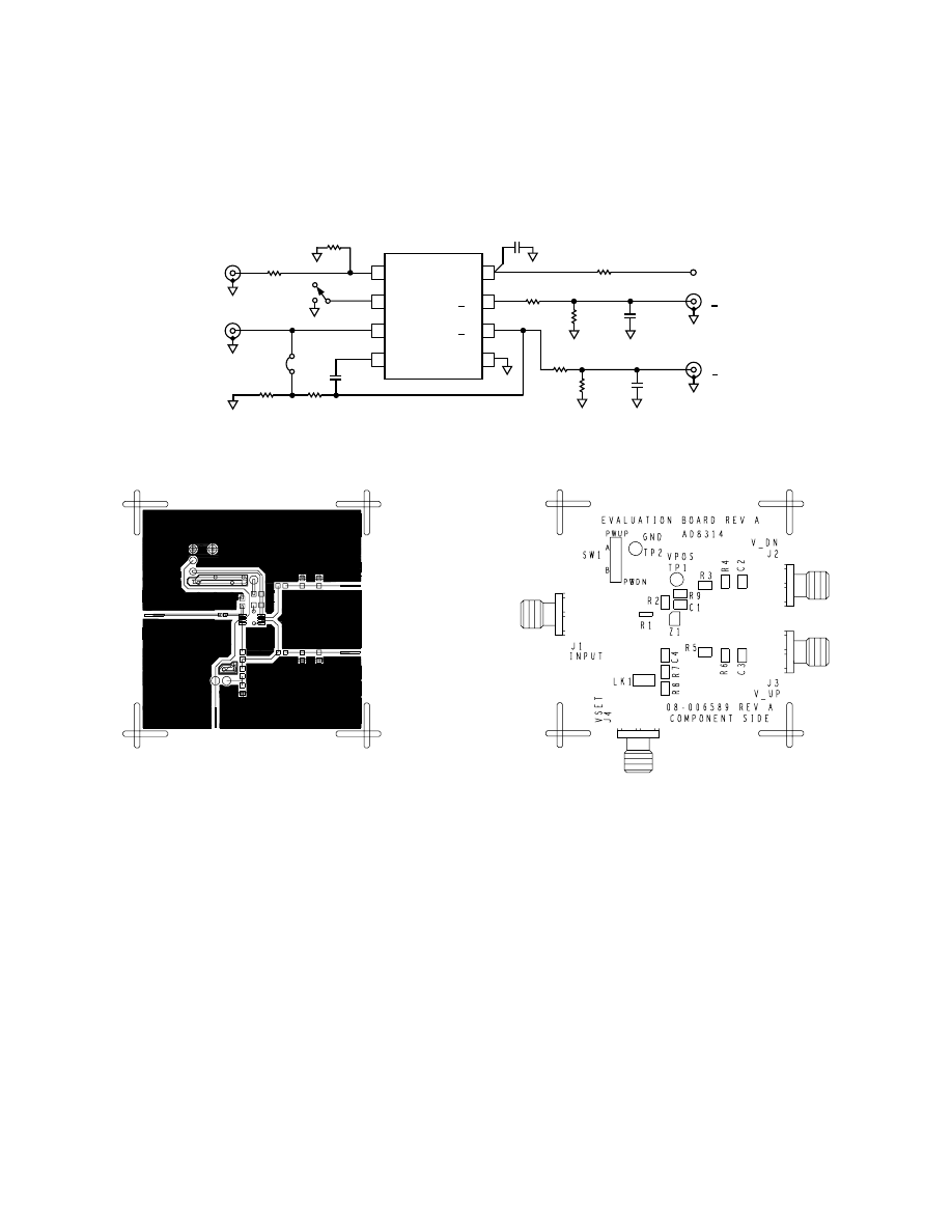
Figure 38. Evaluation Board Schematic
Figure 39. Layout of Component Side
Figure 40. Silkscreen of Component Side
EVALUATION BOARD
Figure 38 shows the schematic of the AD8314 evaluation board.
The layout and silkscreen of the component side are shown in
Figures 39 and 40. The board is powered by a single supply
in the range, 2.7 V to 5.5 V. The power supply is decoupled
by a single 0.1
µ
F capacitor. Additional decoupling, in the form
of a series resistor or inductor in R9, can also be added. Table IV
details the various configuration options of the evaluation board.

AD8314
–15–
REV. 0
Table IV. Evaluation Boards Configuration Options
Component
Function
Default Condition
TP1, TP2
Supply and Ground Vector Pins
Not Applicable
SW1
Device Enable: When in position A, the ENBL
SW1 = A
pin is connected to +V
S
and the AD8314 is in
operating mode. In Position B, the ENBL pin is
grounded, putting the device in power-down mode.
R1, R2
Input Interface: The 52.3
Ω
resistor in position
R2 = 52.3
Ω
(Size 0603)
R2 combines with the AD8314’s internal input
R1 = 0
Ω
(Size 0402)
impedance to give a broadband input impedance
of around 50
Ω
. A reactive match can be imple-
mented by replacing R2 with an inductor and
R1 (0
Ω
) with a capacitor. Note that the AD8314’s
RF input is internally ac-coupled.
R3, R4, C2, R5, R6, C3
Output Interface: R4, C2, R6, and C3 can be
R4 = C2 = R6 = C3 = Open (Size 0603)
used to check the response of V_UP and V_DN
R3 = R5 = 0
Ω
(Size 0603)
to capacitive and resistive loading. R3/R4 and
R5/R6 can be used to reduce the slope of V_UP
and V_DN.
C1, R9
Power Supply Decoupling: The nominal supply
C1 = 0.1
µ
F (Size 0603)
decoupling consists of a 0.1
µ
F capacitor (C1). A
R9 = 0
Ω
(Size 0603)
series inductor or small resistor can be placed in
R9 for additional decoupling.
C4
Filter Capacitor: The response time of V_UP
C4 = Open (Size 0603)
and V_DN can be modified by placing a capacitor
between FLTR (pin 4) and V_UP.
R7, R8
Slope Adjust: By installing resistors in R7 and R8,
R7 = 0
Ω
(Size 0603)
the nominal slope of 20 mV/dB can be increased.
R8 = Open (Size 0603)
See Slope Adjust discussion for more details.
LK1
Measurement/Controller Mode: LK1 shorts
LK1 = Installed
V_UP to VSET, placing the AD8314 in
measurement mode. Removing LK1 places
the AD8314 in controller mode.
–16–
C2726–4.5–10/99
PRINTED IN U.S.A.
REV. 0
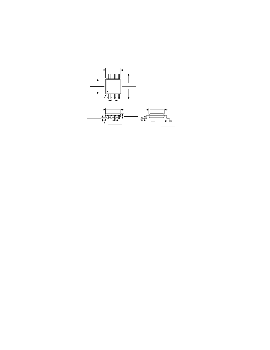
OUTLINE DIMENSIONS
Dimensions shown in inches and (mm).
8-Lead micro_SOIC
(RM-8)
0.011 (0.28)
0.003 (0.08)
0.028 (0.71)
0.016 (0.41)
33
8
27
8
0.120 (3.05)
0.112 (2.84)
8
5
4
1
0.122 (3.10)
0.114 (2.90)
0.199 (5.05)
0.187 (4.75)
PIN 1
0.0256 (0.65) BSC
0.122 (3.10)
0.114 (2.90)
SEATING
PLANE
0.006 (0.15)
0.002 (0.05)
0.018 (0.46)
0.008 (0.20)
0.043 (1.09)
0.037 (0.94)
0.120 (3.05)
0.112 (2.84)
AD8314
Wyszukiwarka
Podobne podstrony:
Detekcja czestotliwosci radiowy Nieznany (2)
Detekcja czestotliwosci radiowy Nieznany (3)
Czestosciomierz radiowy id 1273 Nieznany
czestosciomierz radiowy id 1287 Nieznany
Czestosciomierz radiowy id 1273 Nieznany
3 pomiar czestotliwosci fazy c Nieznany
cw01 pomiar czestotliwosci id 1 Nieznany
Zakresy częstotliwości radiowych, Elektronika, Różne
3 pomiar czestotliwosci fazy c Nieznany
cw01 pomiar czestotliwosci id 1 Nieznany
Badanie odbiornika radiowego id Nieznany (2)
Arkana radiowego internetu 2 id Nieznany (2)
Częstotliwości programów radiowych
Arkana radiowego internetu id 6 Nieznany
PRZEMIENNIKI CZESTOTLIWOSCI W D Nieznany
Olsztyn k Częstochowy Archeolodzy odsłonili nieznaną kondygnację zamku
więcej podobnych podstron