MSP430x13x, MSP430x14x
MIXED SIGNAL MICROCONTROLLER
SLAS272C – JULY 2000 – REVISED FEBRUARY 2001
1
POST OFFICE BOX 655303
•
DALLAS, TEXAS 75265
D
Low Supply-Voltage Range, 1.8 V . . . 3.6 V
D
Ultralow-Power Consumption:
– Standby Mode: 1.6
µ
A
– RAM Retention Off Mode: 0.1
µ
A
D
Low Operating Current:
– 2.5
µ
A at 4 kHz, 2.2 V
– 280
µ
A at 1 MHz, 2.2 V
D
Five Power-Saving Modes
D
Wake-Up From Standby Mode in 6
µ
s
D
16-Bit RISC Architecture,
125-ns Instruction Cycle Time
D
12-Bit A/D Converter With Internal
Reference, Sample-and-Hold and Autoscan
Feature
D
16-Bit Timer With Seven
Capture/Compare-With-Shadow Registers,
Timer_B
D
16-Bit Timer With Three Capture/Compare
Registers, Timer_A
D
On-Chip Comparator
D
Serial Onboard Programming,
No External Programming Voltage Needed
Programmable Code Protection by Security
Fuse
D
Family Members Include:
– MSP430F133:
8KB+256B Flash Memory,
256B RAM
– MSP430F135:
16KB+256B Flash Memory,
512B RAM
– MSP430F147:
32KB+256B Flash Memory,
1KB RAM
– MSP430F148:
48KB+256B Flash Memory,
2KB RAM
– MSP430F149:
60KB+256B Flash Memory,
2KB RAM
D
Available in 64-Pin Quad Flat Pack (QFP)
description
The Texas Instruments MSP430 series is an ultralow-power microcontroller family consisting of several devices
featuring different sets of modules targeted to various applications. The microcontroller is designed to be battery
operated for use in extended-time applications. The MSP430 achieves maximum code efficiency with its 16-bit
RISC architecture, 16-bit CPU-integrated registers, and a constant generator. The digitally-controlled oscillator
provides wake-up from low-power mode to active mode in less than 6
µ
s. The MSP430x13x and the
MSP430x14x series are microcontroller configurations with two built-in 16-bit timers, a fast 12-bit A/D converter,
one or two universal serial synchronous/asynchronous communication interfaces (USART), and 48 I/O pins.
Typical applications include sensor systems that capture analog signals, convert them to digital values, and
process and transmit the data to a host system. The timers make the configurations ideal for industrial control
applications such as ripple counters, digital motor control, EE-meters, hand-held meters, etc. The hardware
multiplier enhances the performance and offers a broad code and hardware-compatible family solution.
AVAILABLE OPTIONS
PACKAGED DEVICES
TA
PLASTIC 64-PIN QFP
(PM)
–40
°
C to 85
°
C
MSP430F133IPM
MSP430F135IPM
MSP430F147IPM
MSP430F148IPM
MSP430F149IPM
Copyright
2001, Texas Instruments Incorporated
PRODUCTION DATA information is current as of publication date.
Products conform to specifications per the terms of Texas Instruments
standard warranty. Production processing does not necessarily include
testing of all parameters.
Please be aware that an important notice concerning availability, standard warranty, and use in critical applications of
Texas Instruments semiconductor products and disclaimers thereto appears at the end of this data sheet.
MSP430x13x, MSP430x14x
MIXED SIGNAL MICROCONTROLLER
SLAS272C – JULY 2000 – REVISED FEBRUARY 2001
2
POST OFFICE BOX 655303
•
DALLAS, TEXAS 75265
pin designation, MSP430F133, MSP430F135
1718 19
P5.4/MCLK
P5.3
P5.2
P5.1
P5.0
P4.7/TBCLK
P4.6
P4.5
P4.4
P4.3
P4.2/TB2
P4.1/TB1
P4.0/TB0
P3.7
P3.6
P3.5/URXD0
48
47
46
45
44
43
42
41
40
39
38
37
36
35
34
33
20
1
2
3
4
5
6
7
8
9
10
11
12
13
14
15
16
DV
CC
P6.3/A3
P6.4/A4
P6.5/A5
P6.6/A6
P6.7/A7
V
REF+
XIN
XOUT/TCLK
Ve
REF+
V
REF–
/Ve
REF–
P1.0/TACLK
P1.1/TA0
P1.2/TA1
P1.3/TA2
P1.4/SMCLK
21 22 23 24
P5.6/ACLK
TDO/TDI
63 62 61 60 59
64
58
AV
P6.2/A2
P6.1/A1
P6.0/A0
RST/NMI
TCK
TMS
P2.6/ADC12CLK
P2.7/T
A0
P3.0/STE0
P3.1/SIMO0
P1.7/T
A2
P2.1/T
AINCLK
P2.2/CAOUT/T
A0
P2.3/CA0/T
A1
P2.4/CA1/T
A2
P2.5/Rosc
56 55 54
57
25 26 27 28 29
53 52
P1.5/T
A0
XT2IN
XT2OUT
51 50 49
30 31 32
P3.2/SOMI0
P3.3/UCLK0
P3.4/UTXD0
P5.7/TBoutH
TDI
P5.5/SMCLK
AV
DV
PM PACKAGE
(TOP VIEW)
P1.6/T
A1
P2.0/ACLK
CC
SS
SS
MSP430x13x, MSP430x14x
MIXED SIGNAL MICROCONTROLLER
SLAS272C – JULY 2000 – REVISED FEBRUARY 2001
3
POST OFFICE BOX 655303
•
DALLAS, TEXAS 75265
pin designation, MSP430F147, MSP430F148, MSP430F149
1718 19
P5.4/MCLK
P5.3/UCLK1
P5.2/SOMI1
P5.1/SIMO1
P5.0/STE1
P4.7/TBCLK
P4.6/TB6
P4.5/TB5
P4.4/TB4
P4.3/TB3
P4.2/TB2
P4.1/TB1
P4.0/TB0
P3.7/URXD1
P3.6/UTXD1
P3.5/URXD0
48
47
46
45
44
43
42
41
40
39
38
37
36
35
34
33
20
1
2
3
4
5
6
7
8
9
10
11
12
13
14
15
16
DV
CC
P6.3/A3
P6.4/A4
P6.5/A5
P6.6/A6
P6.7/A7
V
REF+
XIN
XOUT/TCLK
Ve
REF+
V
REF–
/Ve
REF–
P1.0/TACLK
P1.1/TA0
P1.2/TA1
P1.3/TA2
P1.4/SMCLK
21 22 23 24
P5.6/ACLK
TDO/TDI
63 62 61 60 59
64
58
AV
P6.2/A2
P6.1/A1
P6.0/A0
RST/NMI
TCK
TMS
P2.6/ADC12CLK
P2.7/T
A0
P3.0/STE0
P3.1/SIMO0
P1.7/T
A2
P2.1/T
AINCLK
P2.2/CAOUT/T
A0
P2.3/CA0/T
A1
P2.4/CA1/T
A2
P2.5/Rosc
56 55 54
57
25 26 27 28 29
53 52
P1.5/T
A0
XT2IN
XT2OUT
51 50 49
30 31 32
P3.2/SOMI0
P3.3/UCLK0
P3.4/UTXD0
P5.7/TBoutH
TDI
P5.5/SMCLK
AV
DV
PM PACKAGE
(TOP VIEW)
P1.6/T
A1
P2.0/ACLK
CC
SS
SS
MSP430x13x, MSP430x14x
MIXED SIGNAL MICROCONTROLLER
SLAS272C – JULY 2000 – REVISED FEBRUARY 2001
4
POST OFFICE BOX 655303
•
DALLAS, TEXAS 75265
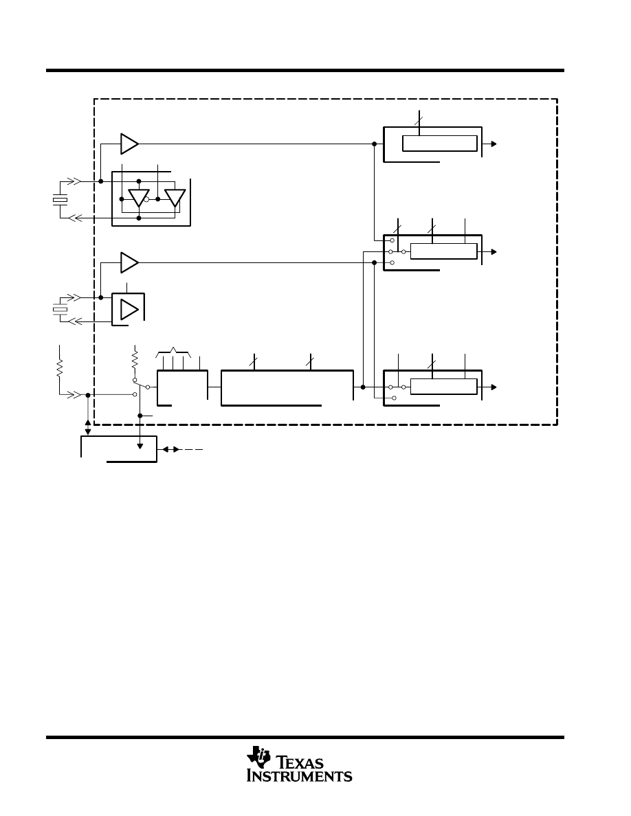
functional block diagrams
MSP430x14x
Oscillator
System
ACLK
SMCLK
2 kB RAM
I/O Port 1/2
16 I/Os, With
I/O Port 3/4
16 I/Os
I/O Port 5
8 I/Os
I/O Port 6
CPU
Incl. 16 Reg.
Test
JTAG
Bus
Conv
Power
USART0
Comparator
Watchdog
Timer_B7
Timer
15 / 16 Bit
7 CC-Reg.
MAB, 4 Bit
MDB, 8 Bit
MCB
XIN
XOUT/TCLK
AVCC
AVSS
RST/NMI
P3
P4
P5
P6
XT2IN
XT2OUT
TMS
TCK
60 kB Flash
48 kB Flash
12 Bit ADC
8 Channels
<10
Timer_A3
Emulation
Module
MDB, 16 Bit
MAB, 16 Bit
Clock
Rosc
MCLK
4
TDI
TDO/TDI
ACLK
SMCLK
Shadow
Reg.
3 CC-Reg.
on
Reset
UART Mode
SPI Mode
USART1
UART Mode
32 kB Flash
2 kB RAM
1 kB RAM
µ
s Conv.
Interrupt
Capability
P1
P2
8 I/Os
DVSS
DVCC
Multipy
MPY, MPYS
MAC,MACS
8
×
8 Bit
8
×
16 Bit
16
×
8 Bit
16
×
16 Bit
A
SPI Mode
MSP430x13x
Oscillator
System
ACLK
SMCLK
I/O Port 1/2
16 I/Os, With
I/O Port 3/4
16 I/Os
I/O Port 5
8 I/Os
I/O Port 6
CPU
Incl. 16 Reg.
Test
JTAG
Bus
Conv
Power
USART0
Comparator
Watchdog
Timer_B3
Timer
15 / 16 Bit
3 CC-Reg.
MAB, 4 Bit
MDB, 8 Bit
MCB
XIN
XOUT/TCLK
AVCC
AVSS
RST/NMI
P3
P4
P5
P6
XT2IN
XT2OUT
TMS
TCK
16 kB Flash
8 kB Flash
12 Bit ADC
8 Channels
<10
Timer_A3
Emulation
Module
MDB, 16 Bit
MAB, 16 Bit
Clock
Rosc
MCLK
4
TDI
TDO/TDI
ACLK
SMCLK
Shadow
Reg.
3 CC-Reg.
on
Reset
UART Mode
SPI Mode
512B RAM
µ
s Conv.
Interrupt
Capability
P1
P2
8 I/Os
DVSS
DVCC
256B RAM
A
MSP430x13x, MSP430x14x
MIXED SIGNAL MICROCONTROLLER
SLAS272C – JULY 2000 – REVISED FEBRUARY 2001
5
POST OFFICE BOX 655303
•
DALLAS, TEXAS 75265
Terminal Functions
TERMINAL
I/O
DESCRIPTION
NAME
NO.
I/O
DESCRIPTION
AVCC
64
Analog supply voltage, positive terminal. Supplies only the analog portion of the analog-to-digital converter.
AVSS
62
Analog supply voltage, negative terminal. Supplies only the analog portion of the analog-to-digital converter.
DVCC
1
Digital supply voltage, positive terminal. Supplies all digital parts.
DVSS
63
Digital supply voltage, negative terminal. Supplies all digital parts.
P1.0/TACLK
12
I/O
General digital I/O pin/Timer_A, clock signal TACLK input
P1.1/TA0
13
I/O
General digital I/O pin/Timer_A, capture: CCI0A input, compare: Out0 output
P1.2/TA1
14
I/O
General digital I/O pin/Timer_A, capture: CCI1A input, compare: Out1 output
P1.3/TA2
15
I/O
General digital I/O pin/Timer_A, capture: CCI2A input, compare: Out2 output
P1.4/SMCLK
16
I/O
General digital I/O pin/SMCLK signal output
P1.5/TA0
17
I/O
General digital I/O pin/Timer_A, compare: Out0 output
P1.6/TA1
18
I/O
General digital I/O pin/Timer_A, compare: Out1 output
P1.7/TA2
19
I/O
General digital I/O pin/Timer_A, compare: Out2 output/
P2.0/ACLK
20
I/O
General digital I/O pin/ACLK output
P2.1/TAINCLK
21
I/O
General digital I/O pin/Timer_A, clock signal at INCLK
P2.2/CAOUT/TA0
22
I/O
General digital I/O pin/Timer_A, capture: CCI0B input/Comparator_A output
P2.3/CA0/TA1
23
I/O
General digital I/O pin/Timer_A, compare: Out1 output/Comparator_A input
P2.4/CA1/TA2
24
I/O
General digital I/O pin/Timer_A, compare: Out2 output/Comparator_A input
P2.5/Rosc
25
I/O
General-purpose digital I/O pin, input for external resistor defining the DCO nominal frequency
P2.6/ADC12CLK
26
I/O
General digital I/O pin, conversion clock – 12-bit ADC
P2.7/TA0
27
I/O
General digital I/O pin/Timer_A, compare: Out0 output
P3.0/STE0
28
I/O
General digital I/O, slave transmit enable – USART0/SPI mode
P3.1/SIMO0
29
I/O
General digital I/O, slave in/master out of USART0/SPI mode
P3.2/SOMI0
30
I/O
General digital I/O, slave out/master in of USART0/SPI mode
P3.3/UCLK0
31
I/O
General digital I/O, external clock input – USART0/UART or SPI mode, clock output – USART0/SPI mode
P3.4/UTXD0
32
I/O
General digital I/O, transmit data out – USART0/UART mode
P3.5/URXD0
33
I/O
General digital I/O, receive data in – USART0/UART mode
P3.6/UTXD1†
34
I/O
General digital I/O, transmit data out – USART1/UART mode
P3.7/URXD1†
35
I/O
General digital I/O, receive data in – USART1/UART mode
P4.0/TB0
36
I/O
General-purpose digital I/O, capture I/P or PWM output port – Timer_B7 CCR0
P4.1/TB1
37
I/O
General-purpose digital I/O, capture I/P or PWM output port – Timer_B7 CCR1
P4.2/TB2
38
I/O
General-purpose digital I/O, capture I/P or PWM output port – Timer_B7 CCR2
P4.3/TB3†
39
I/O
General-purpose digital I/O, capture I/P or PWM output port – Timer_B7 CCR3
P4.4/TB4†
40
I/O
General-purpose digital I/O, capture I/P or PWM output port – Timer_B7 CCR4
P4.5/TB5†
41
I/O
General-purpose digital I/O, capture I/P or PWM output port – Timer_B7 CCR5
P4.6/TB6†
42
I/O
General-purpose digital I/O, capture I/P or PWM output port – Timer_B7 CCR6
P4.7/TBCLK
43
I/O
General-purpose digital I/O, input clock TBCLK – Timer_B7
P5.0/STE1†
44
I/O
General-purpose digital I/O, slave transmit enable – USART1/SPI mode
P5.1/SIMO1†
45
I/O
General-purpose digital I/O slave in/master out of USART1/SPI mode
P5.2/SOMI1†
46
I/O
General-purpose digital I/O, slave out/master in of USART1/SPI mode
P5.3/UCLK1†
47
I/O
General-purpose digital I/O, external clock input – USART1/UART or SPI mode, clock output – USART1/SPI
mode
P5.4/MCLK
48
I/O
General-purpose digital I/O, main system clock MCLK output
P5.5/SMCLK
49
I/O
General-purpose digital I/O, submain system clock SMCLK output
† 14x devices only
General-Purpose Register
Program Counter
Stack Pointer
Status Register
Constant Generator
General-Purpose Register
General-Purpose Register
General-Purpose Register
PC/R0
SP/R1
SR/CG1/R2
CG2/R3
R4
R5
R14
R15
MSP430x13x, MSP430x14x
MIXED SIGNAL MICROCONTROLLER
SLAS272C – JULY 2000 – REVISED FEBRUARY 2001
6
POST OFFICE BOX 655303
•
DALLAS, TEXAS 75265
Terminal Functions (Continued)
TERMINAL
I/O
DESCRIPTION
NAME
NO.
I/O
DESCRIPTION
P5.6/ACLK
50
I/O
General-purpose digital I/O, auxiliary clock ACLK output
P5.7/TboutH
51
I/O
General-purpose digital I/O, switch all PWM digital output ports to high impedance – Timer_B7 TB0 to TB6
P6.0/A0
59
I/O
General digital I/O, analog input a0 – 12-bit ADC
P6.1/A1
60
I/O
General digital I/O, analog input a1 – 12-bit ADC
P6.2/A2
61
I/O
General digital I/O, analog input a2 – 12-bit ADC
P6.3/A3
2
I/O
General digital I/O, analog input a3 – 12-bit ADC
P6.4/A4
3
I/O
General digital I/O, analog input a4 – 12-bit ADC
P6.5/A5
4
I/O
General digital I/O, analog input a5 – 12-bit ADC
P6.6/A6
5
I/O
General digital I/O, analog input a6 – 12-bit ADC
P6.7/A7
6
I/O
General digital I/O, analog input a7 – 12-bit ADC
RST/NMI
58
I
Reset input, nonmaskable interrupt input port, or bootstrap loader start (in Flash devices).
TCK
57
I
Test clock. TCK is the clock input port for device programming test and bootstrap loader start (in Flash
devices).
TDI
55
I
Test data input. TDI is used as a data input port. The device protection fuse is connected to TDI.
TDO/TDI
54
I/O
Test data output port. TDO/TDI data output or programming data input terminal
TMS
56
I
Test mode select. TMS is used as an input port for device programming and test.
VeREF+
10
I/P
Input for an external reference voltage to the ADC
VREF+
7
O
Output of positive terminal of the reference voltage in the ADC
VREF–/VeREF–
11
O
Negative terminal for the ADC’s reference voltage for both sources, the internal reference voltage, or an
external applied reference voltage
XIN
8
I
Input port for crystal oscillator XT1. Standard or watch crystals can be connected.
XOUT/TCLK
9
I/O
Output terminal of crystal oscillator XT1 or test clock input
XT2IN
53
I
Input port for crystal oscillator XT2. Only standard crystals can be connected.
XT2OUT
52
O
Output terminal of crystal oscillator XT2
short-form description
processing unit
The processing unit is based on a consistent and orthogonal CPU and instruction set. This design structure
results in a RISC-like architecture, highly transparent to the application development and notable for its ease
of programming. All operations other than program-flow instructions are consequently performed as register
operations in conjunction with seven addressing modes for source and four modes for destination operand.
CPU
The CPU has sixteen registers that provide
reduced instruction execution time. This reduces
the register-to-register operation execution time
to one cycle of the processor frequency.
Four of the registers are reserved for special use
as program counter, stack pointer, status register,
and constant generator. The remaining registers
are available as general-purpose registers.
Peripherals are connected to the CPU using a
data address and control bus, and can be easily
handled with all memory manipulation instruc-
tions.
MSP430x13x, MSP430x14x
MIXED SIGNAL MICROCONTROLLER
SLAS272C – JULY 2000 – REVISED FEBRUARY 2001
7
POST OFFICE BOX 655303
•
DALLAS, TEXAS 75265
short-form description (continued)
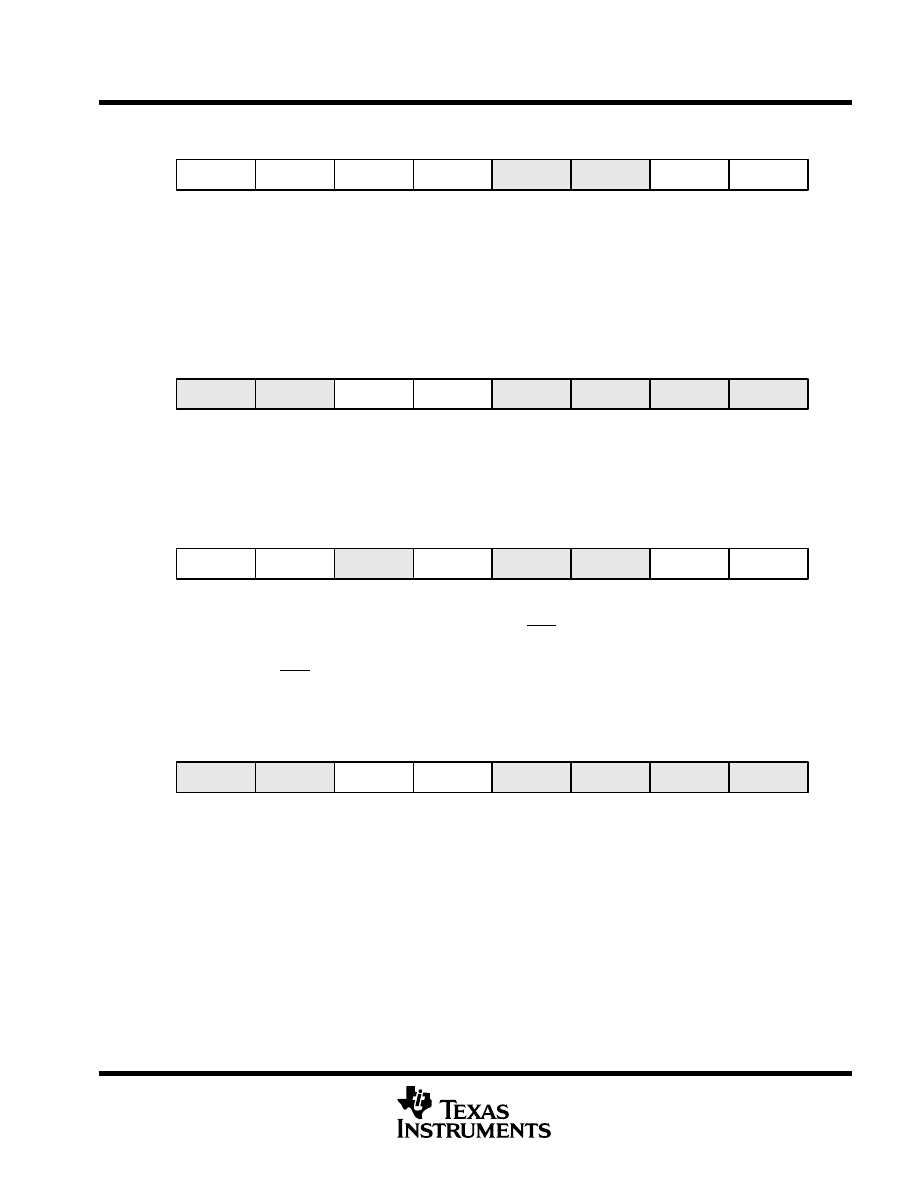
instruction set
The instruction set for this register-to-register architecture constitutes a powerful and easy-to-use assembler
language. The instruction set consists of 51 instructions with three formats and seven address modes. Table 1
provides a summary and example of the three types of instruction formats; the address modes are listed in
Table 2.
Table 1. Instruction Word Formats
Dual operands, source-destination
e.g. ADD R4,R5
R4 + R5 –––> R5
Single operands, destination only
e.g. CALL R8
PC ––>(TOS), R8––> PC
Relative jump, un/conditional
e.g. JNE
Jump-on-equal bit = 0
Each instruction operating on word and byte data is identified by the suffix B.
Examples:
WORD INSTRUCTIONS
BYTE INSTRUCTIONS
MOV
EDE, TONI
MOV.B
EDE,TONI
ADD
#235h,&MEM
ADD.B
#35h,&MEM
PUSH
R5
PUSH.B
R5
SWPB
R5
—
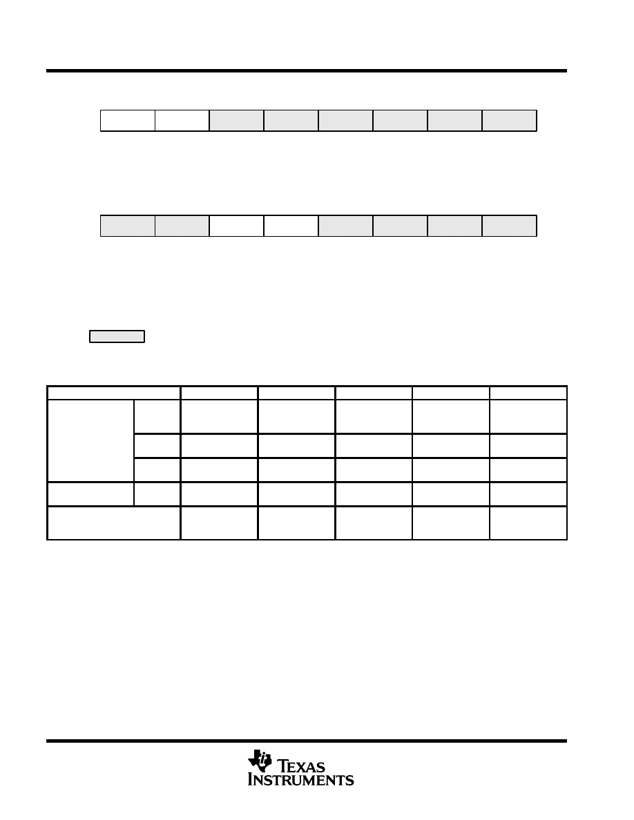
Table 2. Address Mode Descriptions
ADDRESS MODE
S
D
SYNTAX
EXAMPLE
OPERATION
Register
n n
MOV Rs,Rd
MOV R10,R11
R10 ––> R11
Indexed
n n
MOV X(Rn),Y(Rm)
MOV 2(R5),6(R6)
M(2+R5)––> M(6+R6)
Symbolic (PC relative)
n n
MOV EDE,TONI
M(EDE) ––> M(TONI)
Absolute
n n
MOV &MEM,&TCDAT
M(MEM) ––> M(TCDAT)
Indirect
n
MOV @Rn,Y(Rm)
MOV @R10,Tab(R6)
M(R10) ––> M(Tab+R6)
Indirect
autoincrement
n
MOV @Rn+,Rm
MOV @R10+,R11
M(R10) ––> R11
R10 + 2––> R10
Immediate
n
MOV #X,TONI
MOV #45,TONI
#45 ––> M(TONI)
NOTE: S = source D = destination
Computed branches (BR) and subroutine call (CALL) instructions use the same address modes as other
instructions. These address modes provide indirect addressing, which is ideally suited for computed branches
and calls. The full use of this programming capability results in a program structure which is different from
structures used with conventional 8- and 16-bit controllers. For example, numerous routines can be easily
designed to deal with pointers and stacks instead of using flag-type programs for flow control.
operating modes and interrupts
The MSP430 operating modes provide advanced support of the requirements for ultralow-power and ultralow-
energy consumption. This goal is achieved by intelligent management during the different operating modes of
modules and CPU states and is fully supported during interrupt event handling. An interrupt event awakes the
system from each of the various operating modes and returns, using the RETI instruction, to the mode that was
selected before the interrupt event occurred. The different requirements on CPU and modules—driven by
system cost and current consumption objectives—require the use of different clock signals:
D
Auxiliary clock ACLK, sourced by LFXT1CLK (crystal frequency) and used by the peripheral modules
D
Main system clock MCLK, used by the CPU and system
D
Subsystem clock SMCLK, used by the peripheral modules
MSP430x13x, MSP430x14x
MIXED SIGNAL MICROCONTROLLER
SLAS272C – JULY 2000 – REVISED FEBRUARY 2001
8
POST OFFICE BOX 655303
•
DALLAS, TEXAS 75265
operating modes and interrupts (continued)
/1, /2, /4, /8
2
ACLK
Auxiliary Clock
ACLKGEN
OscOff
XTS
LFXT1 Oscillator
High Frequency
XT1 Oscillator, XTS = 1
DIVA
Low Power
LF Oscillator, XTS = 0
XIN
XOUT
/1, /2, /4, /8, Off
2
MCLK
Main System
Clock
MCLKGEN
SELM
2
DIVM
CPUOff
XT2Off
XT2IN
XT2OUT
XT2 Oscillator
/1, /2, /4, /8, Off
SMCLK
SUB-System
Clock
SMCLKGEN
SELS
2
DIVS
SCG1
DCOMOD
Digital Controlled Oscillator DCO
+
Modulator MOD
3
DCO
5
MOD
DCOCLK
DC
Generator
Rsel
SCG0
0.1
LFXT1CLK
XT2CLK
VCC
VCC
P2.5
The DCO generator is connected to pin P2.5/Rosc if DCOR control bit is set.
The port pin P2.5/Rosc is selected if DCOR control bit is reset (initial state).
DCGEN
DCOR
0
1
0
1
3
2
P2.5/Rosc
Any of these clock sources—LFXT1CLK, XT2CLK, or DCOCLK—can be used to drive the MSP430 system.
LFXT1CLK is defined by connecting a low-power, low-frequency crystal to the oscillator, by connecting a
high-frequency crystal to the oscillator, or by applying an external clock source. The high-frequency crystal
oscillator is used if control bit XTS is set. The crystal oscillator may be switched off if LFXT1CLK is not required
for the current operating mode.
XT2CLK is defined by connecting a high-frequency crystal to the oscillator or by applying an external clock
source. Crystal oscillator XT2 may be switched off using the XT2Off control bit if not required by the current
operating mode.
When DCOCLK is active, its frequency is selected or adjusted by software. DCOCLK is inactive or stopped when
it is not being used by the CPU or peripheral modules. The dc generator can be stopped when SCG0 is reset
and DCOCLK is not required. The dc generator determines the basic DCO frequency, and can be set by one
external resistor or adjusted in eight steps by selection of integrated resistors.
NOTE:
The system clock generator always starts with DCOCLK selected as MCLK (CPU clock) to ensure proper start
of program execution. The software determines the final system clock through control bit manipulation.
The system clock MCLK is also selected by hardware to be the DCOCLK (DCO and DCGEN are on) if the crystal
oscillator (XT1 or XT2) fails while being selected as MCLK. Without this forced clock mode the NMI, requested
by the oscillator fault flag, can not be handled and control may be lost. Without forced-clock mode the processor
could not execute any code until the failed oscillator restarts.
MSP430x13x, MSP430x14x
MIXED SIGNAL MICROCONTROLLER
SLAS272C – JULY 2000 – REVISED FEBRUARY 2001
9
POST OFFICE BOX 655303
•
DALLAS, TEXAS 75265
low-power consumption capabilities
The various operating modes are handled by software by controlling the operation of the internal clock system.
This clock system provides a large combination of hardware and software capabilities to run the application
while maintaining the lowest power consumption and optimizing system costs. This is accomplished by:
D
Use of the internal clock (DCO) generator without any external components
D
Selection of an external crystal or ceramic resonator for lowest frequency and cost
D
Selection and activation of the proper clock signals (LFXT1CLK, XT2Off, and/or DCOCLK) and clock
predivider function. Control bit XT2Off is embedded in control register BCSCTL1.
D
Application of an external clock source
The control bits that most influence the operation of the clock system and support fast turnon from low power
operating modes are located in the status register SR. Four bits control the CPU and the system clock generator:
SCG1, SCG0, OscOff, and CPUOff.
Reserved For Future
Enhancements
15
9
8
7
0
V
SCG1
SCG0
OscOff
CPUOff
GIE
N
Z
C
rw-0
CPUOff, SCG1, SCG0, and OscOff are the most important bits in low-power control when the basic function
of the system clock generator is established. They are pushed to the stack whenever an interrupt is accepted
and saved for returning to the operation before an interrupt request. They can be manipulated via indirect access
to the data on the stack during execution of an interrupt handler so that program execution can resume in
another power operating mode after return-from-interrupt.
CPUOff:
Clock signal MCLK, used with the CPU, is active when the CPUOff bit is reset or stopped when
set.
SCG1:
Clock signal SMCLK, used with peripherals, is enabled when the SCG1 bit is reset or stopped
when set.
OscOff:
Crystal oscillator LFXT1 is active when the OscOff bit is reset. The LFXT1 oscillator can be inac-
tive only when the OscOff bit is set and it is not used for MCLK. The setup time to start a crystal
oscillation requires special consideration when the off option is used. Mask-programmable de-
vices can disable this feature and the oscillator can never be switched off by software.
SCG0:
The dc generator is active when the SCG0 bit is reset. The DCO can be inactive only if the SCG0
bit is set and the DCOCLK signal is not used as MCLK or SMCLK. The dc current consumed
by the dc generator defines the basic frequency of the DCOCLK.
When the current is switched off (SCG0=1) the start of the DCOCLK is slightly delayed. This
delay is in the microsecond range.
DCOCLK:
Clock signal DCOCLK is stopped if not used as MCLK or SMCLK. There are two situations when
the SCG0 bit can not switch the DCOCLK signal off:
The DCOCLK frequency is used as MCLK (CPUOff=0 and SELM.1=0), or the DCOCLK
frequency is used as SMCLK (SCG1=0 and SELS=0).
If DCOCLK is required for operation, the SCG0 bit can not switch the dc generator off.
MSP430x13x, MSP430x14x
MIXED SIGNAL MICROCONTROLLER
SLAS272C – JULY 2000 – REVISED FEBRUARY 2001
10
POST OFFICE BOX 655303
•
DALLAS, TEXAS 75265
interrupt vector addresses
The interrupt vectors and the power-up starting address are located in the address range 0FFFFh – 0FFE0h.
The vector contains the 16-bit address of the appropriate interrupt-handler instruction sequence.
INTERRUPT SOURCE
INTERRUPT FLAG
SYSTEM INTERRUPT
WORD ADDRESS
PRIORITY
Power-up
External Reset
Watchdog
Flash memory
WDTIFG
KEYV
(see Note 1)
Reset
0FFFEh
15, highest
NMI
Oscillator Fault
Flash memory access violation
NMIIFG (see Notes 1 & 4)
OFIFG (see Notes 1 & 4)
ACCVIFG (see Notes 1 & 4)
(Non)maskable
(Non)maskable
(Non)maskable
0FFFCh
14
Timer_B7 (see Note 5)
BCCIFG0 (see Note 2)
Maskable
0FFFAh
13
Timer_B7 (see Note 5)
BCCIFG1 to BCCIFG6
TBIFG (see Notes 1 & 2)
Maskable
0FFF8h
12
Comparator_A
CAIFG
Maskable
0FFF6h
11
Watchdog timer
WDTIFG
Maskable
0FFF4h
10
USART0 receive
URXIFG0
Maskable
0FFF2h
9
USART0 transmit
UTXIFG0
Maskable
0FFF0h
8
ADC
ADCIFG (see Notes 1 & 2)
Maskable
0FFEEh
7
Timer_A3
CCIFG0 (see Note 2)
Maskable
0FFECh
6
Timer_A3
CCIFG1,
CCIFG2,
TAIFG (see Notes 1 & 2)
Maskable
0FFEAh
5
I/O port P1 (eight flags)
P1IFG.0 (see Notes 1 & 2)
To
P1IFG.7 (see Notes 1 & 2)
Maskable
0FFE8h
4
USART1 receive
URXIFG1
Maskable
0FFE6h
3
USART1 transmit
UTXIFG1
0FFE4h
2
I/O port P2 (eight flags)
P2IFG.0 (see Notes 1 & 2)
To
P2IFG.7 (see Notes 1 & 2)
Maskable
0FFE2h
1
0FFE0h
0, lowest
NOTES:
1. Multiple source flags
2. Interrupt flags are located in the module.
3. Nonmaskable: neither the individual nor the general interrupt-enable bit will disable an interrupt event.
4. (Non)maskable: the individual interrupt-enable bit can disable an interrupt event, but the general-interrupt enable can not disable
it.
5. Timer_B7 in MSP430x14x family has 7 CCRs; Timer_B3 in MSP430x13x family has 3 CCRs; in Timer_B3 there are only interrupt
flags CCIFG0, 1, and 2, and the interrupt-enable bits CCIE0, 1, and 2 integrated.
special function registers
Most interrupt and module-enable bits are collected in the lowest address space. Special-function register bits
not allocated to a functional purpose are not physically present in the device. This arrangement provides simple
software access.
MSP430x13x, MSP430x14x
MIXED SIGNAL MICROCONTROLLER
SLAS272C – JULY 2000 – REVISED FEBRUARY 2001
11
POST OFFICE BOX 655303
•
DALLAS, TEXAS 75265
interrupt enable 1 and 2
7
6
5
4
0
UTXIE0
OFIE
WDTIE
3
2
1
rw-0
rw-0
rw-0
Address
0h
URXIE0
ACCVIE
NMIIE
rw-0
rw-0
rw-0
WDTIE:
Watchdog-timer-interrupt enable signal
OFIE:
Oscillator-fault-interrupt enable signal
NMIIE:
Nonmaskable-interrupt enable signal
ACCVIE:
(Non)maskable-interrupt enable signal, access violation if FLASH memory/module is busy
URXIE0:
USART0, UART, and SPI receive-interrupt enable signal
UTXIE0:
USART0, UART, and SPI transmit-interrupt enable signal
7
6
5
4
0
UTXIE1
3
2
1
rw-0
rw-0
Address
01h
URXIE1
URXIE1:
USART1, UART, and SPI receive-interrupt enable signal
UTXIE1:
USART1, UART, and SPI transmit-interrupt enable signal
interrupt flag register 1 and 2
7
6
5
4
0
UTXIFG0
OFIFG
WDTIFG
3
2
1
rw-0
rw-1
rw-0
Address
02h
URXIFG0
NMIIFG
rw-1
rw-0
WDTIFG:
Set on overflow or security key violation or
reset on VCC power-on or reset condition at RST/NMI
OFIFG:
Flag set on oscillator fault
NMIIFG:
Set via RST/NMI pin
URXIFG0:
USART0, UART, and SPI receive flag
UTXIFG0:
USART0, UART, and SPI transmit flag
7
6
5
4
0
UTXIFG1
3
2
1
rw-1
rw-0
Address
03h
URXIFG1
URXIFG1:
USART1, UART, and SPI receive flag
UTXIFG1:
USART1, UART, and SPI transmit flag
MSP430x13x, MSP430x14x
MIXED SIGNAL MICROCONTROLLER
SLAS272C – JULY 2000 – REVISED FEBRUARY 2001
12
POST OFFICE BOX 655303
•
DALLAS, TEXAS 75265
module enable registers 1 and 2
7
6
5
4
0
UTXE0
3
2
1
rw-0
rw-0
Address
04h
URXE0
USPIE0
URXE0:
USART0, UART receive enable
UTXE0:
USART0, UART transmit enable
USPIE0:
USART0, SPI (synchronous peripheral interface) transmit and receive enable
7
6
5
4
0
UTXE1
3
2
1
rw-0
rw-0
Address
05h
URXE1
USPIE1
URXE1:
USART1, UART receive enable
UTXE1:
USART1, UART transmit enable
USPIE1:
USART1, SPI (synchronous peripheral interface) transmit and receive enable
rw-0:
Legend: rw:
Bit Can Be Read and Written
Bit Can Be Read and Written. It Is Reset by PUC.
SFR Bit Not Present in Device
memory organization
MSP430F133
MSP430F135
MSP430F147
MSP430F148
MSP430F149
Memory
Main: interrupt vector
Main: code memory
Size
Flash
Flash
8kB
0FFFFh – 0FFE0h
0FFFFh – 0E000h
16kB
0FFFFh – 0FFE0h
0FFFFh – 0C000h
32kB
0FFFFh – 0FFE0h
0FFFFh – 08000h
48kB
0FFFFh – 0FFE0h
0FFFFh – 04000h
60kB
0FFFFh – 0FFE0h
0FFFFh – 01100h
Information memory
Size
Flash
256 Byte
010FFh – 01000h
256 Byte
010FFh – 01000h
256 Byte
010FFh – 01000h
256 Byte
010FFh – 01000h
256 Byte
010FFh – 01000h
Boot memory
Size
ROM
1kB
0FFFh – 0C00h
1kB
0FFFh – 0C00h
1kB
0FFFh – 0C00h
1kB
0FFFh – 0C00h
1kB
0FFFh – 0C00h
RAM
Size
256 Byte
02FFh – 0200h
512 Byte
03FFh – 0200h
1kB
05FFh – 0200h
2kB
09FFh – 0200h
2kB
09FFh – 0200h
Peripherals
16-bit
8-bit
8-bit SFR
01FFh – 0100h
0FFh – 010h
0Fh – 00h
01FFh – 0100h
0FFh – 010h
0Fh – 00h
01FFh – 0100h
0FFh – 010h
0Fh – 00h
01FFh – 0100h
0FFh – 010h
0Fh – 00h
01FFh – 0100h
0FFh – 010h
0Fh – 00h
boot ROM containing bootstrap loader
The intention of the bootstrap loader is to download data into the flash memory module. Various write, read, and
erase operations are needed for a proper download environment. The bootstrap loader is only available on F
devices.
functions of the bootstrap loader:
Definition of read:
Apply and transmit data of peripheral registers or memory to pin P1.1 (BSLTX)
write:
Read data from pin P2.2 (BSLRX) and write them into flash memory
unprotected functions
Mass erase, erase of the main memory (segment 0 to segment n) and information memory (segment A and
segment B)
Access to the MSP430 via the bootstrap loader is protected. It must be enabled before any protected function
can be performed. The 256 bits in 0FFE0h to 0FFFFh provide the access key.

MSP430x13x, MSP430x14x
MIXED SIGNAL MICROCONTROLLER
SLAS272C – JULY 2000 – REVISED FEBRUARY 2001
13
POST OFFICE BOX 655303
•
DALLAS, TEXAS 75265
boot ROM containing bootstrap loader (continued)
protected functions
All protected functions can be executed only if the access is enabled.
D
Write/program byte into flash memory; parameters passed are start address and number of bytes (the
segment-write feature of the flash memory is not supported and not useful with the UART protocol).
D
Segment erase of segment 0 to segment n in main memory, and segment erase of segments A and B in
the information memory.
D
Read all data in main memory and information memory.
D
Read and write to all byte peripheral modules and RAM.
D
Modify PC and start program execution immediately.
NOTE:
Unauthorized readout of code and data is prevented by the user’s definition of the data in the
interrupt memory locations.
features of the bootstrap loader are:
D
UART communication protocol, fixed to 9600 baud
D
Port pin P1.1 for transmit, P2.2 for receive
D
TI standard serial protocol definition
D
Implemented in flash memory version only
D
Program execution starts with the user vector at 0FFFEh or with the bootstrap loader (start vector is at
address 0C00h)
hardware resources used for serial input/output:
D
Pins P1.1 and P2.2 for serial data transmission
D
TCK and RST/NMI to start program execution at the reset or bootstrap loader vector
D
Basic clock module:
Rsel=5, DCO=4, MOD=0, DCOCLK for MCLK and SMCLK, clock divider for MCLK
and SMCLK at default: dividing by 1
D
Timer_A: Timer_A operates in continuous mode with MCLK source selected, input divider set to 1,
using CCR0, and polling of CCIFG0.
D
WDT:
Watchdog Timer is halted
D
Interrupt: GIE=0, NMIIE=0, OFIE=0, ACCVIE=0
D
Memory allocation and stack pointer:
If the stack pointer points to RAM addresses above 0220h, 6 bytes of the stack are allocated,
plus RAM addresses 0200h to 0219h. Otherwise the stack pointer is set to 0220h and allocates
RAM from 0200h to 021Fh.
NOTE:
When writing RAM data via the bootstrap loader, make sure that the stack is outside the
range of the data to be written.
MSP430x13x, MSP430x14x
MIXED SIGNAL MICROCONTROLLER
SLAS272C – JULY 2000 – REVISED FEBRUARY 2001
14
POST OFFICE BOX 655303
•
DALLAS, TEXAS 75265
boot ROM containing bootstrap loader (continued)
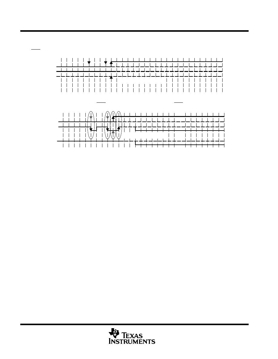
Program execution begins with the user’s reset vector at FFFEh (standard method) if TCK is held high while
RST/NMI goes from low to high:
User Program Starts
RST/NMI
TCK
Program execution begins with the bootstrap vector at 0C00h (boot ROM) if a minimum of two negative edges
have been applied to TCK while RST/NMI is low, and TCK is low when RST/NMI goes from low to high.
Bootloader Starts
RST/NMI
TCK
TMS
The bootstrap loader will not start (via the vector in address 0C00h) if:
D
There are less than two negative edges at TCK while RST/NMI is low
D
TCK is high when RST/NMI goes from low to high
D
JTAG has control over the MSP430 resources
D
The supply voltage VCC drops and a POR is executed
NOTES:
6. The default level of TCK is high. An active low has to be applied to enter the bootstrap loader. Other MSP430s which have a pin
function used with a low default level can use an inverted signal.
7. The TMS signal must be high while TCK clocks are applied. This ensures that the JTAG controller function remains in its default
mode.
WARNING:
The bootstrap loader starts correctly only if the RST/NMI pin is in reset mode. Unpredictable
program execution may result if it is switched to the NMI function. However, a bootstrap load
may be started using software and the bootstrap vector, for example using the instruction
BR &0C00h.

MSP430x13x, MSP430x14x
MIXED SIGNAL MICROCONTROLLER
SLAS272C – JULY 2000 – REVISED FEBRUARY 2001
15
POST OFFICE BOX 655303
•
DALLAS, TEXAS 75265
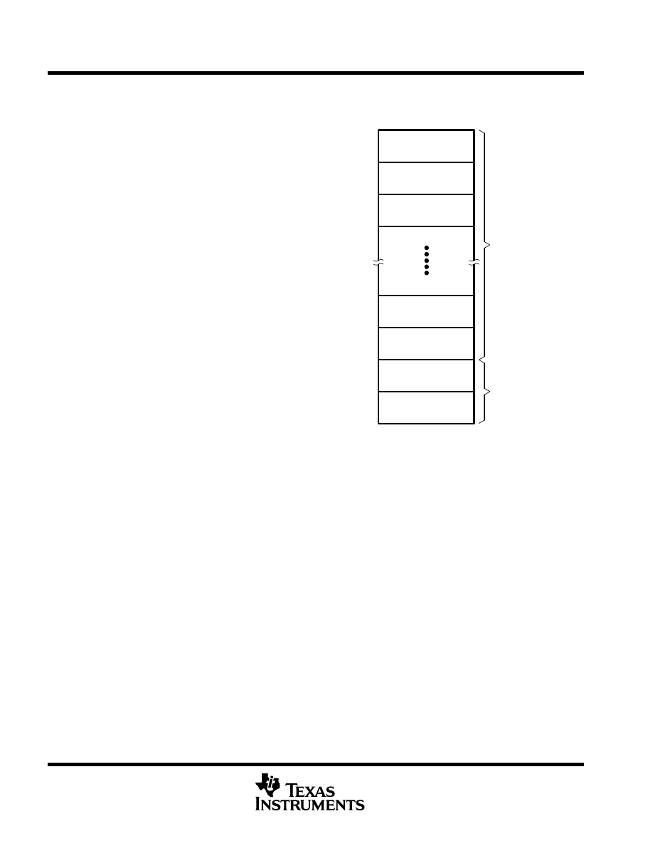
flash memory
D
Flash memory has n segments of main memory and two segments of information memory (A and B) of 128
bytes each. Each segment in main memory is 512 bytes in size.
D
Segments 0 to n may be erased in one step, or each segment may be individually erased.
D
Segments A and B can be erased individually, or as a group with segments 0–n.
Segments A and B are also called information memory.
D
A security fuse burning is irreversible; no further access to JTAG is possible afterwards
D
Internal generation of the programming/erase voltage: no external V
PP
has to be applied, but V
CC
increases
the supply current requirements.
D
Program and erase timing is controlled by hardware in the flash memory – no software intervention is
needed.
D
The control hardware is called the flash-timing generator. The input frequency of the flash–timing generator
should be in the proper range and should be maintained until the write/program or erase operation is
completed.
D
During program or erase, no code can be executed from flash memory and all interrupts must be disabled
by setting the GIE, NMIIE, ACCVIE, and OFIE bits to zero. If a user program requires execution concurrent
with a flash program or erase operation, the program must be executed from memory other than the flash
memory (e.g., boot ROM, RAM). In the event a flash program or erase operation is initiated while the
program counter is pointing to the flash memory, the CPU will execute JMP $ instructions until the flash
program or erase operation is completed. Normal execution of the previously running software then
resumes.
D
Unprogrammed, new devices may have some bytes programmed in the information memory (needed for
test during manufacturing). The user should perform an erase of the information memory prior to first use.
MSP430x13x, MSP430x14x
MIXED SIGNAL MICROCONTROLLER
SLAS272C – JULY 2000 – REVISED FEBRUARY 2001
16
POST OFFICE BOX 655303
•
DALLAS, TEXAS 75265
flash memory (continued)
Segment 0
w/ Interrupt Vectors
Segment 1
Segment 2
Segment n-1
Segment n
Segment A
Segment B
Main
Memory
Information
Memory
8 kB
0FFFFh
0FE00h
0FDFFh
0FC00h
0FBFFh
0FA00h
0F9FFh
16 kB
0FFFFh
0FE00h
0FDFFh
0FC00h
0FBFFh
0FA00h
0F9FFh
32 kB
0FFFFh
0FE00h
0FDFFh
0FC00h
0FBFFh
0FA00h
0F9FFh
48 kB
0FFFFh
0FE00h
0FDFFh
0FC00h
0FBFFh
0FA00h
0F9FFh
60 kB
0FFFFh
0FE00h
0FDFFh
0FC00h
0FBFFh
0FA00h
0F9FFh
0E400h
0E3FFh
0E200h
0E1FFh
0E000h
010FFh
01080h
0107Fh
01000h
0C400h
0C3FFh
0C200h
0C1FFh
0C000h
010FFh
01080h
0107Fh
01000h
08400h
083FFh
08200h
081FFh
08000h
010FFh
01080h
0107Fh
01000h
04400h
043FFh
04200h
041FFh
04000h
010FFh
01080h
0107Fh
01000h
01400h
013FFh
01200h
011FFh
01100h
010FFh
01080h
0107Fh
01000h
MSP430x13x, MSP430x14x
MIXED SIGNAL MICROCONTROLLER
SLAS272C – JULY 2000 – REVISED FEBRUARY 2001
17
POST OFFICE BOX 655303
•
DALLAS, TEXAS 75265
flash memory, control register FCTL1
All control bits are reset during PUC. PUC is active after application of V
CC
, application of a reset condition to
the RST/NMI pin, expiration of the Watchdog Timer, occurrence of a watchdog access violation, or execution
of an improper flash operation. A more detailed description of the control-bit functions is found in the
flash-memory module description (in the MSP430x1xx user’s guide, literature number SLAU049). Any write to
control register FCTL1 during erase, mass erase, or write (programming) will end in an access violation with
ACCVIFG=1. In an active segment-write mode the control register can be written if the wait mode is active
(WAIT=1). Special conditions apply during segment-write mode. See the MSP430x1xx user’s guide for details.
Read access is possible at any time without restrictions.
The bits of control register FCTL1 are:
rw-0
15
0
SEG
WRT
8
7
WRT
res.
res.
res.
MEras Erase
res.
rw-0
r0
r0
r0
rw-0
rw-0
r0
096h
0A5h
FCTL1
0128h
FCTL1 Read:
FCTL1 Write:
Erase
0128h, bit1
Erase a segment
0: No segment erase will be started.
1: Erase of one segment is enabled. The segment to be erased is defined by a
dummy write into any address within the segment. The erase bit is
automatically reset when the erase operation is completed. See Note 8.
MEras
0128h, bit2
Mass erase, Segment0 to Segmentn are erased together.
0: No erase will be started
1: Erase of Segment0 to Segmentn is enabled. A dummy write to any address in
Segment0 to Segmentn starts mass erase. The MEras bit is automatically reset
when the erase operation is completed. See Note 8.
WRT
0128h, bit6
Bit WRT should be set for a successful write operation.
An access violation occurs and ACCVIFG is set if bit WRT is reset and write
access to the flash memory is performed. See Note 8.
SEGWRT
0128h, bit7
Bit SEGWRT may be used to reduce total programming time.
Segment-write bit SEGWRT is useful when larger sequences of data have to be
programmed. After completion of programming of one segment, a reset and set
sequence has to be performed to enable access to the next segment. The WAIT
bit must be high before executing the next write instruction.
0: No segment write accelerate is selected.
1: Segment write is used. This bit needs to be reset and set between segment
borders.
NOTE 8: Only instruction-fetch access is allowed during program, erase, or mass-erase cycles. Any other access to the flash memory
during these cycles will result in setting the ACCVIFG bit. An NMI interrupt should handle such violations.
MSP430x13x, MSP430x14x
MIXED SIGNAL MICROCONTROLLER
SLAS272C – JULY 2000 – REVISED FEBRUARY 2001
18
POST OFFICE BOX 655303
•
DALLAS, TEXAS 75265
flash memory, control register FCTL1 (continued)
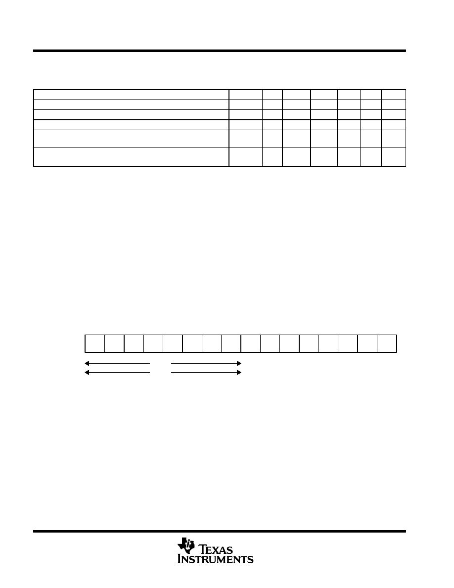
Table 3. Valid Combinations of Control Bits for Flash Memory Access (see Note 9)
FUNCTION PERFORMED
SEGWRT
WRT
MERAS
ERASE
BUSY
WAIT
LOCK
Write word or byte
0
1
0
0
0
0
0
Write word or byte in same segment, segment write mode
1
1
0
0
0
1
0
Erase one segment by writing to any address in the target segment
0
0
0
1
0
0
0
Erase all segments (0 to n) but not the information memory (segments A
and B)
0
0
1
0
0
0
0
Erase all segments (0 to n, and A and B) by writing to any address in
the flash memory module
0
0
1
1
0
0
0
NOTE 9: The table shows all possible combinations of control bits SEGWRT, WRT, MEras, Erase, and BUSY. All other combinations will result
in an access violation.
flash memory, timing generator, control register FCTL2
The timing generator (Figure 1) produces all the timing signals necessary for write, erase, and mass erase (see
NOTE below) from the selected clock source. One of three different clock sources may be selected by control
bits SSEL0 and SSEL1 in control register FCTL2. The selected clock source should be divided to meet the
frequency requirements specified in the recommended operating conditions.
NOTE:
The mass erase duration generated by the flash timing generator is at least 11.1 ms. The
cummulative mass erase time needed is 200 ms. This can be achieved by repeating the mass erase
operation until the cumulative mass erase time is met (a minimum of 19 cycles may be required).
The flash-timing generator is reset with PUC. It is also reset if the emergency exit bit EMEX is set. Control
register FCTL2 may not be written to if the BUSY bit is set; otherwise, an access violation will occur
(ACCVIFG=1).
Read access is possible at any time without restrictions.
rw-0
15
0
SSEL1
8
7
FN5
rw-1
rw-0
rw-1
096h
0A5h
FCTL2
012Ah
FCTL2 Read:
FCTL2 Write:
SSEL0
FN4
FN3
FN2
FN1
FN0
rw-0
rw-0
rw-0
rw-0
The control bits are:
FN0 to
FN5
012Ah, bit0
012Ah, bit5
These six bits determine the division rate of the clock signal. The division rate is 1
to 64, depending on the value of FN5 to FN0 plus one.
SSEL0
012Ah, bit0
Determine the clock source
SSEL1
0: ACLK
1: MCLK
2: SMCLK
3: SMCLK
MSP430x13x, MSP430x14x
MIXED SIGNAL MICROCONTROLLER
SLAS272C – JULY 2000 – REVISED FEBRUARY 2001
19
POST OFFICE BOX 655303
•
DALLAS, TEXAS 75265
flash memory control register FCTL3
There are no restrictions on modifying this control register. The control bits are reset or set (WAIT) by a PUC,
but key violation bit KEYV is reset with a POR.
rw-1
15
0
ACCV
IFG
8
7
EMEX
res.
res.
WAIT
KEYV
BUSY
rw-0
r0
r0
r-1
rw-0
rw-(0)
096h
0A5h
FCTL3
012Ch
FCTL3 Read:
FCTL3 Write:
Lock
r(w)-0
BUSY
012Ch, bit0
The BUSY bit shows if an access to the flash memory is correct (BUSY=0), or if an access
violation has taken place. The BUSY bit should be tested before each write and erase cycle.
0: Flash memory is not busy.
1: Flash memory is busy. It remains in busy state if segment-write function is in wait mode.
KEYV,
012Ch, bit1
Key violated
0: Key 0A5h (high byte) was not violated.
1: Key 0A5h (high byte) was violated. Violation occurs when a write access to register
FCTL1, FCTL2, or FCTL3 is executed and the high byte is not equal to 0A5h. If the
security key is violated, bit KEYV is set and a PUC is performed.
ACCVIFG,
012Ch, bit2
Access-violation interrupt flag
The access-violation interrupt flag is set only when a write or erase operation is active.
Access violation can only happen if the flash-memory module is written or read while it is
busy. An instruction can be fetched during write, erase, and mass erase, but not during
segment write. When the access-violation interrupt-enable bit is set, the interrupt-service
request is accepted and the program continues at the NMI interrupt-vector address.
Reading the control registers will not set the ACCVIFG bit.
WAIT,
012Ch, bit3
In the segment-write mode, the WAIT bit indicates that the flash memory is prepared to
receive the (next) data for programming. The WAIT bit is read only, but a write to WAIT bit
is allowed.
0: Segment-write operation is started and programming is in progress
1: Segment write operation is active and programming of data has been completed
Lock
012Ch, bit4
The lock bit may be set during any write, erase of a segment, or mass erase request. The
active sequence is completed normally. In segment-write mode, the SEGWRT and WAIT
bits are reset and the mode ends in the regular manner. The software or hardware controls
the lock bit. If an access violation occurs during segment-write mode, the ACCVIFG and
LOCK bits may be set.
0: Flash memory may be read, programmed, erased, and mass erased.
1: Flash memory may be read but not programmed, erased, and mass-erased. A current
program, erase, or mass-erase operation will complete normally. The access-violation
interrupt flag ACCVIFG is set when the flash-memory module is accessed while the lock
bit is set.
EMEX,
012Ch, bit5
Emergency exit. The emergency exit should only be used if a flash memory write or erase
operation is out of control.
0: No function
1: Stops the active operation immediately and shuts down all internal parts in the flash
memory controller. Current consumption immediately drops back to the active mode
level. All bits in control register FCTL1 are reset. Since the EMEX bit is automatically
reset by hardware, the software always reads EMEX as 0.
MSP430x13x, MSP430x14x
MIXED SIGNAL MICROCONTROLLER
SLAS272C – JULY 2000 – REVISED FEBRUARY 2001
20
POST OFFICE BOX 655303
•
DALLAS, TEXAS 75265
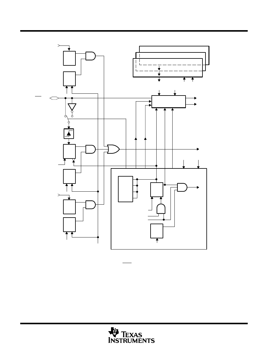
flash memory, interrupt and security key violation
System Reset
Generator
PUC
POR
VCC
S
Clear
PUC
NMIIFG
OFIFG
S
IFG1.0
Clear
OFIE
IE1.1
PUC
NMI_IRQA
S
Clear
Counter
S
Clear
IE1.0
PUC
WDTIE
WDTIFG
IRQ
POR
NMIES
TMSEL
NMI
WDTQn
EQU
PUC
POR
Watchdog Timer Module
IRQA: Interrupt Request Accepted
IRQA
TIMSEL
IFG1.1
OSCFault
IFG1.4
RST/NMI
NMIRS
Clear
NMIIE
IE1.1
PUC
S
ACCVIFG
FCTL1.1
Clear
ACCVIE
IE1.5
PUC
ACCV
KEYV
Flash Module
Flash Module
Flash Module
PUC
POR
Figure 1. Block Diagram of NMI Interrupt Sources
One NMI vector is used for three NMI events: RST/NMI (NMIIFG), oscillator fault (OFIFG), and flash memory
access violation (ACCVIFG). The software can determine the source of the interrupt request, since all flags
remain set until reset by software. The enable flag(s) should be set only within one instruction directly before
the return-from-interrupt (RETI) instruction. This ensures that the stack remains under control. A pending NMI
interrupt request will not increase stack demand unnecessarily.

MSP430x13x, MSP430x14x
MIXED SIGNAL MICROCONTROLLER
SLAS272C – JULY 2000 – REVISED FEBRUARY 2001
21
POST OFFICE BOX 655303
•
DALLAS, TEXAS 75265
peripherals
Peripherals are connected to the CPU through data, address, and control busses, and can be easily handled
using all memory-manipulation instructions.
oscillator and system clock
Three clocks are used in the system—the main system (master) clock (MCLK) used by the CPU and the system,
the subsystem (master) clock (SMCLK) used by the peripheral modules, and the auxiliary clock (ACLK)
originated by LFXT1CLK (crystal frequency) and used by the peripheral modules.
Following a POR the DCOCLK is used by default, the DCOR bit is reset, and the DCO is set to the nominal initial
frequency. Additionally, if either LFXT1CLK (with XT1 mode selected by XTS=1) or XT2CLK fails as the source
for MCLK, DCOCLK is automatically selected to ensure fail-safe operation.
SMCLK can be generated from XT2CLK or DCOCLK. ACLK is always generated from LFXT1CLK.
Crystal oscillator LFXT1 can be defined to operate with watch crystals (32,768 Hz) or with higher-frequency
ceramic resonators or crystals. The crystal or ceramic resonator is connected across two terminals. No external
components are required for watch-crystal operation. If the high-frequency XT1 mode is selected, external
capacitors from XIN to VSS and XOUT to VSS are required, as specified by the crystal manufacturer.
The LFXT1 oscillator starts after application of VCC. If the OscOff bit is set to 1, the oscillator stops when it is
not used for MCLK.
Crystal oscillator XT2 is identical to oscillator LFXT1, but only operates with higher-frequency ceramic
resonators or crystals. The crystal or ceramic resonator is connected across two terminals. External capacitors
from XT2IN to VSS and XT2OUT to VSS are required as specified by the crystal manufacturer.
The XT2 oscillator is off after application of VCC, since the XT2 oscillator control bit XT2Off is set. If bit XT2Off
is set to 1, the XT2 oscillator stops when it is not used for MCLK or SMCLK.
Clock signals ACLK , MCLK, and SMCLK may be used externally via port pins.
Different application requirements and system conditions dictate different system-clock requirements,
including:
D
High frequency for quick reaction to system hardware requests or events
D
Low frequency to minimize current consumption, EMI, etc.
D
Stable peripheral clock for timer applications, such as real-time clock (RTC)
D
Start-stop operation that can be enabled with minimum delay
multiplication
The multiplication operation is supported by a dedicated peripheral module. The module performs 16x16, 16x8,
8x16, and 8x8 bit operations. The module is capable of supporting signed and unsigned multiplication as well
as signed and unsigned multiply and accumulate operations. The result of an operation can be accessed
immediately after the operands have been loaded into the peripheral registers. No additional clock cycles are
required.
digital I/O
There are six 8-bit I/O ports implemented—ports P1 through P6. Ports P1 and P2 use seven control registers,
while ports P3, P4, P5, and P6 use only four of the control registers to provide maximum digital input/output
flexibility to the application:
D
All individual I/O bits are independently programmable.
D
Any combination of input, output, and interrupt conditions is possible.
D
Interrupt processing of external events is fully implemented for all eight bits of ports P1 and P2.
D
Read/write access to all registers using all instructions is possible.

MSP430x13x, MSP430x14x
MIXED SIGNAL MICROCONTROLLER
SLAS272C – JULY 2000 – REVISED FEBRUARY 2001
22
POST OFFICE BOX 655303
•
DALLAS, TEXAS 75265
digital I/O (continued)
The seven control registers are:
D
Input register
8 bits at ports P1 through P6
D
Output register
8 bits at ports P1 through P6
D
Direction register
8 bits at ports P1 through P6
D
Interrupt edge select
8 bits at ports P1 and P2
D
Interrupt flags
8 bits at ports P1 and P2
D
Interrupt enable
8 bits at ports P1 and P2
D
Selection (port or module)
8 bits at ports P1 through P6
Each one of these registers contains eight bits. Two interrupt vectors are implemented: one commonly used
for any interrupt event on ports P1.0 to P1.7, and another commonly used for any interrupt event on ports P2.0
to P2.7.
Ports P3, P4, P5, and P6 have no interrupt capability.
Watchdog Timer
The primary function of the Watchdog Timer (WDT) module is to perform a controlled system restart after a
software upset has occurred. A system reset is generated if the selected time interval expires. If an application
does not require this watchdog function, the module can work as an interval timer, which generates an interrupt
after a selected time interval.
The Watchdog Timer counter (WDTCNT) is a 15/16-bit up-counter not directly accessible by software. The
WDTCNT is controlled using the Watchdog Timer control register (WDTCTL), which is an 8-bit read/write
register. Writing to WDTCTL in either operating mode (watchdog or timer) is only possible when using the correct
password (05Ah) in the high-byte. If any value other than 05Ah is written to the high-byte of the WDTCTL, a
system reset PUC is generated. The password is read as 069h to minimize accidental write operations to the
WDTCTL register. The low-byte stores data written to the WDTCTL. In addition to the Watchdog Timer control
bits, there are two bits included in the WDTCTL that configure the NMI pin.
USART0 and USART1
There are two USART peripherals implemented in the MSP430x14x: USART0 and USART1; but only one in
the MSP430x13x configuration: USART0. Both have an identical function as described in the applicable
chapters of the MSP430x1xx User’s Guide. They use different pins to communicate, and different registers for
module control. Registers with identical functions have different addresses.
The universal synchronous/asynchronous interface is a dedicated peripheral module used in serial communica-
tions. The USART supports synchronous SPI (3- or 4-pin), and asynchronous UART communication protocols,
using double-buffered transmit and receive channels. Data streams of 7 or 8 bits in length can be transferred
at a rate determined by the program, or by an external clock. Low-power applications are optimized by UART
mode options which allow for the reception of only the first byte of a complete frame. The application software
should then decide if the succeeding data is to be processed. This option reduces power consumption.
Two dedicated interrupt vectors are assigned to each USART module—one for the receive and one for the
transmit channels.
MSP430x13x, MSP430x14x
MIXED SIGNAL MICROCONTROLLER
SLAS272C – JULY 2000 – REVISED FEBRUARY 2001
23
POST OFFICE BOX 655303
•
DALLAS, TEXAS 75265
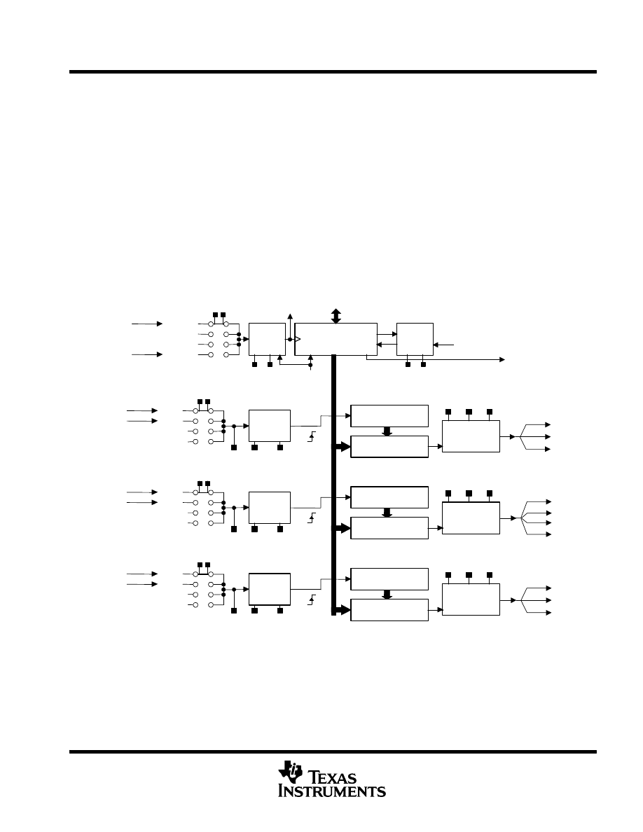
timer_A (three capture/compare registers)
The timer module offers one sixteen-bit counter and three capture/compare registers. The timer clock source
can be selected from two external sources P1.0/TACLK (SSEL=0) or P2.1/TAINCLK (SSEL=3), or from two
internal sources—ACLK (SSEL=1) or SMCLK (SSEL=2). The clock source can be divided by one, two, four,
or eight. The timer can be fully controlled (in word mode)—it can be halted, read, and written; it can be stopped,
run continuously, or made to count up or up/down using one compare block to determine the period. The three
capture/compare blocks are configured by the application to run in capture or compare mode.
The capture mode is mostly used to individually measure internal or external events from any combination of
positive, negative, or positive and negative edges. It can also be stopped by software. Three different external
events can be selected: TA0, TA1, and TA2. In the capture/compare register CCR2, ACLK is the capture signal
if CCI2B is selected. Software capture is chosen if CCISx=2 or CCISx=3.
The compare mode is mostly used to generate timing for the software or application hardware, or to generate
pulse-width modulated output signals for various purposes like D/A conversion functions or motor control. An
individual output module is assigned to each of the three capture/compare registers. This module can run
independently of the compare function or can be triggered in several ways.
15
0
POR/CLR
Timer Clock
Set_TAIFG
Carry/Zero
Data
Equ0
32kHz to 8MHz
TACLK
SMCLK
ACLK
SSEL1 SSEL0
0
1
2
3
INCLK
ID0
ID1
MC0
MC1
Input
Divider
16–bit Timer
Clk
RC
Mode
Control
15
0
Capture/Compare
Capture
CCI0
CCIS00
CCM01CCM00
0
1
2
3
CCIS01
OM01OM00
OM02
Out0
EQU0
CCI0A
CCI0B
VCC
GND
Capture
Mode
Comparator 0
Output Unit0
Timer Bus
15
0
CCI1
CCIS10
CCM11 CCM10
0
1
2
3
CCIS11
OM11 OM10
OM12
Out1
EQU1
CCI1A
CCI1B
Capture
Mode
Comparator 1
Output Unit1
Capture/Compare Reg. CCR1
Capture
15
0
Capture/Compare
CCI2
CCIS20
CCM21CCM20
0
1
2
3
CCIS21
OM21OM20
OM22
Out2
EQU2
CCI2A
CCI2B
Capture
Mode
Comparator 2
Output Unit2
Capture
P1.0/TACLK
P1.5/TA0
P2.1/TAINCLK
P1.1/TA0
P2.2/CAOUT/TA0
P1.2/TA1
CAOUT
from
Comparator_A
P1.3/TA2
ACLK
P1.1/TA0
P2.3/CA0/TA1
P1.6/TA1
ADC12I1
(i/p at ADC12)
P1.7/TA2
P1.3/TA2
P2.4/CA1/TA2
P1.2/TA1
P2.7/TA0
16–bit Timer
Capture/Compare
Register CCR1
Register CCR2
Register CCR0
VCC
GND
VCC
GND
Capture/Compare
Capture/Compare
Figure 2. Timer_A, MSP430x13x/14x Configuration
Two interrupt vectors are used by the module. One vector is assigned to capture/compare block CCR0, and one
common-interrupt vector is implemented for the timer and the other two capture/compare blocks. The three
interrupt events using the same vector are identified by an individual interrupt vector word. The interrupt vector
word is used to add an offset to the program counter so that the interrupt handler software continues at the
corresponding program location. This simplifies the interrupt handler and assigns each interrupt event the same
five-cycle overhead.

MSP430x13x, MSP430x14x
MIXED SIGNAL MICROCONTROLLER
SLAS272C – JULY 2000 – REVISED FEBRUARY 2001
24
POST OFFICE BOX 655303
•
DALLAS, TEXAS 75265
timer_B (7 capture/compare registers in ’x14x and 3 capture/compare registers in ’x13x)
Timer_B7 is identical to Timer_A3, except for the following:
D
The timer counter can be configured to operate in 8-, 10-, 12-, or 16-bit mode.
D
The function of the capture/compare registers is slightly different when in compare mode. In Timer_B, the
compare data is written to the capture/compare register, but is then transferred to the associated compare
latch for the comparison.
D
All output level Outx can be set to Hi-Z from the TboutH external signal.
D
The SCCI bit is not implemented in Timer_B
D
Timer_B7 has seven capture compare registers
The timer module has one sixteen-bit counter and seven capture/compare registers. The timer clock source can
be selected from an external source TBCLK (SSEL=0 or 3), or from two internal sources: ACLK (SSEL=1) and
SMCLK (SSEL=2)). The clock source can be divided by one, two, four, or eight. The timer can be fully controlled
(in word mode): it can be halted, read, and written; it can be stopped, run continuously, or made to count up or
up/down using one compare block to determine the period. The seven capture/compare blocks are configured
by the application to run in capture or in compare mode.
The capture mode is mostly used to measure external or internal events from any combination of positive,
negative, or positive and negative edges. It can also be stopped by software. Any of seven different external
events TB0 to TB6 can be selected. In the capture/compare register CCR6, ACLK is the capture signal if CCI6B
is selected. Software capture is chosen if CCISx=2 or CCISx=3.
The compare mode is mostly used to generate timing for the software or application hardware, or to generate
pulse-width modulated output signals for various purposes such as D/A conversion functions or motor control.
An individual output module is assigned to each of the seven capture/compare registers. This module can run
independently of the compare function, or can be triggered in several ways. The comparison is made from the
data in the compare latches (TBCLx) and not from the compare register.
Two interrupt vectors are used by the module. One vector is assigned to capture/compare block CCR0, and one
common interrupt vector is implemented for the timer and the other six capture/compare blocks. The seven
interrupt events using the same vector are identified by an individual interrupt vector word. The interrupt vector
word is used to add an offset to the program counter so that the interrupt handler software continues at the
corresponding program location. This simplifies the interrupt handler and assigns each interrupt event the same
five-cycle overhead.

MSP430x13x, MSP430x14x
MIXED SIGNAL MICROCONTROLLER
SLAS272C – JULY 2000 – REVISED FEBRUARY 2001
25
POST OFFICE BOX 655303
•
DALLAS, TEXAS 75265
compare latches (TBCLx)
The compare latches can be loaded directly by software or via selected conditions triggered by the PWM
function. They are reset by the POR signal.
Load TBCLx immediate, CLLD=0:
Capture/compare register CCRx and the corresponding compare latch are
loaded simultaneously.
Load TBCLx at Zero, CLLD=1:
The data in capture/compare register CCRx is loaded to the corresponding
compare latch when the 16-bit timer TBR counts to zero.
Load TBCLx at Zero + Period, CLLD=2:
The data in capture/compare register CCRx is loaded to the corresponding
compare latch when the 16-bit timer TBR counts to zero or when the next
period starts (in UP/DOWN mode).
Load TBCLx at EQUx, CLLD=3:
The data in capture/compare register CCRx is loaded when CCRx is equal
to TBR.
Loading the compare latches can be done individually or in groups. Individually means that whenever the
selected load condition (see above) is true, the CCRx data is loaded into TBCLx.
Load TBCLx individually,
TBCLGRP=0:
Compare latch TBCLx is loaded when the selected load condition (CLLD) is true.
Dual load TBCLx mode,
TBCLGRP=1:
Two compare latches TBCLx are loaded when data are written to both CCRx registers of the
same group and the load condition (CLLD) is true. Three groups are defined: CCR1+CCR2,
CCR3+CCR4, and CCR5+CCR6.
Triple load TBCLx mode,
TBCLGRP=2:
Three compare latches TBCLx are loaded when data are written to all CCRx registers of the
same group and then the selected load condition (CLLD) is true. Two groups are defined:
CCR1+CCR2+CCR3 and CR4+CCR5+CCR6.
Full load TBCLx mode,
TBCLGRP=3:
All seven compare latches TBCLx are loaded when data are written to all seven CCRx
registers and then the selected load condition (CLLD) is true. All CCRx data,
CCR0+CCR1+CCR2+CCR3+CCR4+CCR5+CCR6, are simultaneously loaded to the
corresponding SHRx compare latches.
MSP430x13x, MSP430x14x
MIXED SIGNAL MICROCONTROLLER
SLAS272C – JULY 2000 – REVISED FEBRUARY 2001
26
POST OFFICE BOX 655303
•
DALLAS, TEXAS 75265
compare latches (TBCLx) (continued)
15
0
POR/CLR
Timer Clock
Set_TBIFG
Carry/Zero
Data
Equ0
TBCLK
SMCLK
ACLK
SSEL1
SSEL0
0
1
2
3
INCLK
ID0
ID1
MC0
MC1
Input
Divider
16–bit Timer
Clk
RC
Mode
Control
15
0
Capture
CCI0
CCIS00
CCM01 CCM00
0
1
2
3
CCIS01
OM01 OM00
OM02
Out0
EQU0
CCI0A
CCI0B
VCC
GND
Capture
Mode
Comparator 0
Output Unit0
Timer Bus
16–bit Timer
15
0
CCI1
CCIS10
CCM11 CCM10
0
1
2
3
CCIS11
OM11 OM10
OM12
Out1
EQU1
CCI1A
CCI1B
VCC
GND
Capture
Mode
Comparator 1
Output Unit1
Capture
P4.7/
TBCLK
P4.0/TB0
P4.7/
TBCLK
P4.0/TB0
P4.0/TB0
P4.1/TB1
P4.1/TB1
P4.1/TB1
15
0
MDB
15
0
MDB
15
0
CCI6
CCIS60
CCM61 CCM60
0
1
2
3
CCIS61
15
0
OM61 OM60
OM62
Out6
EQU6
CCI6A
CCI6B
VCC
GND
Capture
Mode
Comparator 6
Output Unit6
Capture
P4.6/TB6
P4.6/TB6
MDB
15
0
ACLK
Capture/Compare Reg. CCR2
Capture/Compare Reg. CCR3
Capture/Compare Reg. CCR4
Capture/Compare Reg. CCR5
P4.2/TB2
P4.2/TB2
P4.3/TB3
P4.3/TB3
P4.4/TB4
P4.4/TB4
P4.5/TB5
P4.5/TB5
EQU0
EQU0
EQU0
ADC12I2
i/p at
ADC12
ADC12I3
i/p at
ADC12
Capture/Compare
Register CCR0
Compare Latch
TBCL0
Capture/Compare
Register CCR1
TBCL1
Capture/Compare
Register CCR6
TBCL6
Compare Latch
Compare Latch
MSP430x13x, MSP430x14x
MIXED SIGNAL MICROCONTROLLER
SLAS272C – JULY 2000 – REVISED FEBRUARY 2001
27
POST OFFICE BOX 655303
•
DALLAS, TEXAS 75265
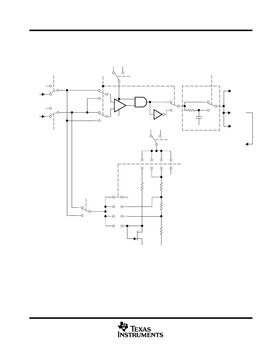
comparator_A
The primary functions of the comparator module are support of precision slope conversion in A/D applications,
battery voltage supervision, and external analog signal monitoring. The comparator is connected to port pins
P2.3 (+ terminal) and to P2.4 (–terminal). It is controlled via eight control bits in the CACTL register.
P2.3/
CA0/
TA1
P2CA0
P2.4/
CA1/
TA2
0
1
0
1
P2CA1
0
1
0
1
_
+
CAON
0
1
CAEX
0
1
CAF
Low Pass Filter
τ
≈
2.0
µ
s
CCI1B
Set CAIFG
Flag
CAOUT
0
CARSEL
1
0
2
1
3
VCAREF
0
1
2
3
CAREF
0.5 x VCC
0.25 x VCC
CA1
CA0
P2.2/
CAOUT/TA0
0 V
0 V
0 V
0 V
VCC
1
0 V
0
CAON
VCC
1
0 V
0

MSP430x13x, MSP430x14x
MIXED SIGNAL MICROCONTROLLER
SLAS272C – JULY 2000 – REVISED FEBRUARY 2001
28
POST OFFICE BOX 655303
•
DALLAS, TEXAS 75265
comparator_A
The control bits are:
CAOUT,
05Ah, bit0
Comparator output
CAF,
05Ah, bit1
The comparator output is transparent or fed through a small filter
P2CA0,
05Ah, bit2
0: Pin P2.3/CA0/TA1 is not connected to Comparator_A.
1: Pin P2.3/CA0/TA1 is connected to Comparator_A.
P2CA1,
05Ah, bit3
0: Pin P2.4/CA1/TA2 is not connected to Comparator_A.
1: Pin P2.4/CA1/TA2 is connected to Comparator_A.
CACTL2.4
to
CATCTL2.7
05Ah, bit4
05Ah, bit7
Bits are implemented but do not control any hardware in this device.
CAIFG,
059h, bit0
Comparator_A interrupt flag
CAIE,
059h, bit1
Comparator_A interrupt enable
CAIES,
059h, bit2
Comparator_A interrupt edge select bit
0: The rising edge sets the Comparator_A interrupt flag CAIFG
1: The falling edge set the Comparator_A interrupt flag CAIFG
CAON,
059h, bit3
The comparator is switched on.
CAREF,
059h, bit4,5
Comparator_A reference
0: Internal reference is switched off, an external reference can be applied.
1: 0.25
×
VCC reference selected.
2: 0.50
×
VCC reference selected.
3: A diode reference selected.
CARSEL,
059h, bit6
An internal reference V
CAREF
, selected by CAREF bits, can be applied to
signal path CA0 or CA1. The signal V
CAREF
is only driven by a voltage
source if the value of CAREF control bits is 1, 2, or 3.
CAEX,
059h, bit7
The comparator inputs are exchanged, used to measure and compensate
the offset of the comparator.
Eight additional bits are implemented into the Comparator_A module. They enable the software to switch off
the input buffer of Port P2. A CMOS input buffer can dissipate supply current when the input is not near V
SS
or V
CC
. Control bits CAPI0 to CAIP7 are initially reset and the port input buffer is active. The port input buffer
is inactive if the corresponding control bit is set.
A/D converter
The 12-bit analog-to-digital converter (ADC) uses a 10-bit weighted capacitor array plus a 2-bit resistor string.
The CMOS threshold detector in the successive-approximation conversion technique determines each bit by
examining the charge on a series of binary-weighted capacitors. The features of the ADC are:
D
12-bit converter with
±
1 LSB linearity
D
Built-in sample-and-hold
D
Eight external and four internal analog channels. The external ADC input terminals are shared with digital
port I/O pins.
D
Internal reference voltage V
REF+
of 1.5 V or 2.5 V, software-selectable by control bit 2_5V
D
Internal-temperature sensor for temperature measurement
T = (V_SENSOR(T) – V_SENSOR(0
°
C)) / TC_SENSOR in
°
C
D
Battery-voltage measurement: N = 0.5
×
(AV
CC
- AV
SS
)
×
4096/1.5V; V
REF
+ is selected for 1.5 V.
D
Source of positive reference voltage level V
R+
can be selected as internal (1.5 V or 2.5 V), external, or AV
CC
.
The source is selected individually for each channel.
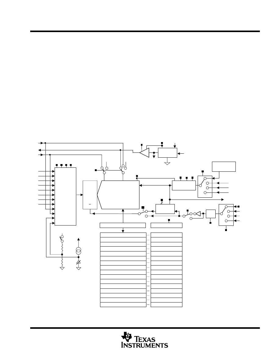
MSP430x13x, MSP430x14x
MIXED SIGNAL MICROCONTROLLER
SLAS272C – JULY 2000 – REVISED FEBRUARY 2001
29
POST OFFICE BOX 655303
•
DALLAS, TEXAS 75265
A/D converter (continued)
D
Source of negative reference voltage level V
R-
can be selected as external or AV
SS
. The source is selected
individually for each channel.
D
Conversion time can be selected from various clock sources: ACLK, MCLK, SMCLK, or the internal
ADC12CLK oscillator. The clock source is divided by an integer from 1 to 8, as selected by software.
D
Channel conversion: individual channels, a group of channels, or repeated conversion of a group of
channels. If conversion of a group of channels is selected, the sequence, the channels, and the number
of channels in the group can be defined by software. For example, a1-a2-a5-a2-a2-
…
.
D
The conversion is enabled by the ENC bit, and can be triggered by software via sample and conversion
control bit ADC12SC, Timer_A3, or Timer_Bx. Most of the control bits can be modified only if ENC control
bit is low. This prevents unpredictable results caused by unintended modification.
D
Sampling time can be 4
×
n0
×
ADC12CLK or 4
×
n1
×
ADC12CLK. It can be selected to sample as long
as the sample signal is high (ISSH=0) or low (ISSH=1). SHT0 defines n0 and SHT1 defines n1.
D
The conversion result is stored in one of sixteen registers. The sixteen registers have individual addresses
and can be accessed via software. Each of the sixteen registers is linked to an 8-bit register that defines
the positive and negative reference source and the channel assigned.
P6.0/A0
P6.1/A1
P6.2/A2
P6.3/A3
P6.4/A4
P6.5/A5
P6.7/A7
P6.6/A6
Analog
Multi–
plexer
12 : 1
AVCC
AVSS
1.5V or 2.5V
AVSS
AVCC
V
REF+
AVCC
AVSS
Sample
&
Hold
ACLK
MCLK
SMCLK
ADC12OSC
Internal
Oscillator
ADC12CLK
S/H
Divide by
1,2,3,4,5,6,7,8
Sampling
Timer
a8
a9
a10
a11
12–bit S A R
ADC12DIV
REFON
2_5V
ISSH
SHP
ADC12CTLx.0..3
ADC12CTLx.4..6
T
SHT1
SHT0
ADC12ON
ADC12SSEL
VeREF
+
V
REF+
V
REF–
/
VeREF–
V
R+
V
R–
12–bit A/D converter core
Conversion CTL
MSC
Ref_X
INCH= 0Ah
Ref_X
SAMPCON
Reference
on
on
0140h
0142h
015Ch
015Eh
080h
081h
08Eh
08Fh
ADC12MEM0
ADC12MEM1
ADC12MEM14
ADC12MEM15
16 x 12–bit
ADC Memory (leading bits 15 to 12 are 0)
16 x 8–bit
ADC Memory Control
ADC12MEM10
ADC12MEM9
ADC12MEM8
ADC12MEM6
ADC12MEM7
ADC12MEM5
ADC12MEM11
ADC12MEM4
ADC12MEM3
ADC12MEM2
ADC12MEM12
ADC12MEM13
ADC12CTL0
ADC12CTL1
ADC12CTL2
ADC12CTL3
ADC12CTL4
ADC12CTL5
ADC12CTL6
ADC12CTL7
ADC12CTL8
ADC12CTL9
ADC12CTL10
ADC12CTL11
ADC12CTL12
ADC12CTL13
ADC12CTL14
ADC12CTL15
082h
083h
084h
085h
086h
088h
087h
089h
08Ah
08Bh
08Ch
08Dh
0144h
0146h
0148h
014Ah
014Ch
014Eh
0150h
0152h
0154h
0156h
0158h
015Ah
SHI
SHS
ENC
ADC12SC
Timer_A3.Out1
Timer_Bx.Out0
Timer_Bx.Out1
SYNC
P2.6/ADC12CLK
MSP430x13x, MSP430x14x
MIXED SIGNAL MICROCONTROLLER
SLAS272C – JULY 2000 – REVISED FEBRUARY 2001
30
POST OFFICE BOX 655303
•
DALLAS, TEXAS 75265
A/D converter (continued)
Table 4. Reference Voltage Configurations
SREF
VOLTAGE AT VR+
VOLTAGE AT VR–
0
AVCC
AVSS
1
VREF+ (internal)
AVSS
2, 3
VeREF+ (external)
AVSS
4
AVCC
VREF–/VeREF– (internal or external)
5
VREF+ (internal)
VREF–/VeREF– (internal or external)
6, 7
VeREF+ (external)
VREF–/VeREF– (internal or external)
control registers ADC12CTL0 and ADC12CTL1
All control bits are reset during POR. POR is active after V
CC
or a reset condition is applied to pin RST/NMI.
A more detailed description of the control bit functions is found in the ADC12 module description (in the user’s
guide). Most of the control bits in registers ADC12CTL0, ADC12CTL1, and ADC12MCTLx can only be modified
if ENC is low.
The following illustration highlights these bits. Six bits are excluded and can be unrestrictedly modified:
ADC12SC, ENC, ADC12TOVIE, ADC12OVIE, and CONSEQ.
The control bits of control registers ADC12CTL0 and ADC12CTL1 are:
01A0h
ADC12CTL0
7
0
15
8
ENC
2_5 V
ADC12
REF
ADC12
TOVIE
ADC12
OVIE
MSC
ADC12
SC
rw–(0)
SHT1
SHT0
ON
ON
rw–(0)
rw–(0)
rw–(0) rw–(0) rw–(0) rw–(0) rw–(0) rw–(0) rw–(0)
ADC12SC
01A0h, bit0
Sample and convert. The ADC12SC bit is used to control the conversion by software. It
is recommended that ISSH=0.
SHP=1: Changing the ADC12SC bit from 0 to 1 starts the sample and conversion
operation. Bit ADC12SC is automatically reset when the conversion is complete
(BUSY=0).
SHP=0: A high level of bit ADC12SC determines the sample time. Conversion starts once
it is reset (by software). The conversion takes 13 ADC12CLK cycles.
ENC
01A0h, bit1
Enable conversion. A conversion can be started by software (via ADC12SC) or by external
signals, only if the enable conversion bit ENC is high. Most of the control bits in
ADC12CTL0 and ADC12CTL1, and all the bits in ADCMCTL.x can only be changed if ENC
is low.
0 :No conversion can be started. This is the initial state.
1: The first sample and conversion starts with the first rising edge of the sampling signal.
The operation selected proceeds as long as ENC is set.
MSP430x13x, MSP430x14x
MIXED SIGNAL MICROCONTROLLER
SLAS272C – JULY 2000 – REVISED FEBRUARY 2001
31
POST OFFICE BOX 655303
•
DALLAS, TEXAS 75265
control registers ADC12CTL0 and ADC12CTL1
ADC12TOVIE
01A0h, bit2
Conversion time overflow interrupt enable.
The timing overflow takes place and a timing overflow vector is generated if another start
of sample and conversion is requested while the current conversion or sequence of
conversions is still active. The timing overflow enable, if set, may request an interrupt.
ADC12OVIE
01A0h, bit3
Overflow interrupt enables the individual enable for the overflow-interrupt vector.
The overflow takes place if the next conversion result is written into ADC memory
ADC12MEMx but the previous result was not read. If an overflow vector is generated, the
overflow-interrupt enable flag ADC12OVIE and the general-interrupt enable GIE are set
and an interrupt service is requested.
ADC12ON
01A0h, bit4
Switch on the 12-bit ADC core. Make sure that the settling timing constraints are met if ADC
core is powered up.
0: Power consumption of the core is off. No conversion is started.
1: ADC core is supplied with power. If no A/D conversion is required, ADC12ON can be
reset to conserve power.
REFON
01A0h, bit5
Reference voltage on
0: The internal reference voltage is switched off. No power is consumed by the reference
voltage generator.
1: The internal reference voltage is switched on and consumes additional power. The
settling time of the reference voltage should be over before the first sample and
conversion is started.
2_5V
01A0h, bit6
Reference voltage level
0: The internal-reference voltage is 1.5 V if REFON = 1.
1: The internal-reference voltage is 2.5 V if REFON = 1.
MSC
01A0h, bit7
Multiple sample and conversion. Works only when the sample timer is selected to generate
the sample signal and to repeat single channel, sequence of channel, or when repeat
sequence of channel (CONSEQ
≠
0) is selected.
0 :Only one sample is taken.
1 :If SHP is set and CONSEQ = {1, 2, or 3}, then the rising edge of the sample timer’s input
signal starts the repeat and/or the sequence of channel mode. Then the second and all
further conversions are immediately started after the current conversion is completed.
SHT0
01A0h, bit8–11
Sample-and-hold Time0
SHT1
01A0h, bit12–15
Sample-and-hold Time1
The sample time is a multiple of the ADC12CLK
×
4:
t
sample
= 4
×
ADC12CLK
×
n
SHT0/1
0
1
2
3
4
5
6
7
8
9
10
11
12–15
n
1
2
4
8
16
24
32
48
64
96
128
192
256
The sampling time defined by SHT0 is used when ADC12MEM0 through ADC12MEM7
are used during conversion. The sampling time defined by SHT1 is used when
ADC12MEM8 through ADC12MEM15 are used during conversion.
MSP430x13x, MSP430x14x
MIXED SIGNAL MICROCONTROLLER
SLAS272C – JULY 2000 – REVISED FEBRUARY 2001
32
POST OFFICE BOX 655303
•
DALLAS, TEXAS 75265
control registers ADC12CTL0 and ADC12CTL1 (continued)
rw–(0) rw–(0) rw–(0) rw–(0)
01A2h
ADC12CTL1
rw–(0) rw–(0) rw–(0) r –(0)
rw–(0) rw–(0) rw–(0) rw–(0)
7
0
15
8
ADC12SSEL
ADC12DIV
CSStartAdd
rw–(0) rw–(0) rw–(0) rw–(0)
CONSEQ
SHS
ISSH
SHP
ADC12
BUSY
ADC12BUSY
01A2h, bit0
The BUSY signal indicates an active sample and conversion operation.
0: No conversion is active. The enable conversion bit ENC can be reset normally.
1: A sample period. Conversion or conversion sequence is active.
CONSEQ
01A2h, bit1/2
Select the conversion mode. Repeat mode is on if CONSEQ.1 (bit 1) is set.
0: One single channel is converted
1: One single sequence of channels is converted
2: Repeating conversion of one single channel
3: Repeating conversion of a sequence of channels
ADC12SSEL
01A2h, bit3/4
Selects the clock source for the converter core
0: Internal oscillator embedded in the ADC12 module
1: ACLK
2: MCLK
3: SMCLK
ADC12DIV
01A2h, bit5,6,7
Selects the division rate for the clock source selected by ADC12SSEL. The clock-opera-
tion signal ADC12CLK is used in the converter core. The conversion, without sampling
time, requires 13 ADC12CLK clocks.
0 to 7: Divide selected clock source by integer from 1 to 8
ISSH
01A2h, bit8
Invert source for the sample signal
0: The source for the sample signal is not inverted.
1: The source for the sample signal is inverted.
SHP
01A2h, bit9
Sample-and-hold pulse, programmable length of sample pulse
0: The sample operation lasts as long as the sample-and-hold signal is 1. The conversion
operation starts if the sample-and-hold signal goes from 1 to 0.
1: The sample time (sample signal is high) is defined by nx4x(1/f
ADC12CLK
). SHTx holds
the data for n. The conversion starts when the sample signal goes from 1 to 0.
SHS
01A2h, bit10/11
Source for sample-and-hold
0: Control bit ADC12SC triggers sample-and-hold followed by the A/D conversion.
1: The trigger signal for sample-and-hold and conversion comes from Timer_A3.EQU1.
2: The trigger signal for sample-and-hold and conversion comes from Timer_B.EQU0.
3: The trigger signal for sample-and-hold and conversion comes from Timer_B.EQU1.
CStartAdd
01A2h, bit12 to
bit15
Conversion start address CstartAdd is used to define which ADC12 control memory is
used to start a (first) conversion. The value of CstartAdd ranges from 0 to 0Fh, correspond-
ing to ADC12MEM0 to ADC12MEM15 and the associated control registers ADC12MCTL0
to ADC12MCTL15.
MSP430x13x, MSP430x14x
MIXED SIGNAL MICROCONTROLLER
SLAS272C – JULY 2000 – REVISED FEBRUARY 2001
33
POST OFFICE BOX 655303
•
DALLAS, TEXAS 75265
control register ADC12MCTLx and conversion memory ADC12MEMx
All control bits are reset during POR. POR is active after application of V
CC
, or after a reset condition is applied
to pin RST/NMI. Control registers ADC12MCTL.x can be modified only if enable conversion control bit ENC is
reset. Any instruction that writes to an ADC12MCTLx register while the ENC bit is reset has no effect. A more
detailed description of the control bit functions is found in the ADC12 module description (in the MSP430x1xx
User’s Guide).
There are sixteen ADC12MCTLx 8-bit memory control registers and sixteen ADC12MEMx 16-bit registers.
Each of the memory control registers is associated with one ADC12MEMx register; for example, ADC12MEM0
is associated with ADC12MCTL0, ADC12MEM1 is associated with ADC12MCTL1, etc.
080h....08Fh
ADC12MCTLx
rw–(0)
rw–(0)
7
0
INCH, Input Channel a0 to a11
Sref, Source of Reference
EOS
rw–(0)
The control register bits are used to select the analog channel, the reference voltage sources for V
R+
and V
R–
,
and a control signal which marks the last channel in a group of channels. The sixteen 16-bit registers
ADC12MEMx are used to hold the conversion results.
The following illustration shows the conversion-result registers ADC12MEM0 to ADC12MEM15:
0
r0
r0
0140h...015Eh
ADC12MEM
15
12
11
r0
r0
rw–(0)
MSB
LSB
0
0
0
0
rw–(0) rw–(0) rw–(0) rw–(0) rw–(0) rw–(0) rw–(0) rw–(0) rw–(0) rw–(0) rw–(0)
ADC12MEM0
to
0140h, bit0,
The 12 bits of the conversion result are stored in 16 control registers
ADC12MEM0 to ADC12MEM15.
ADC12MEM15
015Eh, bit15
The 12 bits are right-justified and the upper four bits are always read as 0.
ADC12 interrupt flags ADC12IFG.x and enable registers ADC12IEN.x
There are 16 ADC12IFG.x interrupt flags, 16 ADC12IE.x interrupt-enable bits, and one interrupt-vector word.
The 16 interrupt flags and enable bits are associated with the 16 ADC12MEMx registers. For example, register
ADC12MEM0, interrupt flag ADC12IFG.0, and interrupt-enable bit ADC12IE.0 form one conversion-result
block.
ADC12IFG.0 has the highest priority and ADC12IFG.15 has the lowest priority.
All interrupt flags and interrupt-enable bits are reset during POR. POR is active after application of V
CC
or after
a reset condition is applied to the RST/NMI pin.
ADC12 interrupt vector register
The 12-bit ADC has one interrupt vector for the overflow flag, the timing overflow flag, and sixteen interrupt flags.
This vector indicates that a conversion result is stored into registers ADC12MEMx. Handling of the 18 flags is
assisted by the interrupt-vector word. The 16-bit vector word ADC12IV indicates the highest pending interrupt.
The interrupt-vector word is used to add an offset to the program counter so that the interrupt-handler software
continues at the corresponding program location according to the interrupt event. This simplifies the interrupt-
handler operation and assigns each interrupt event the same five-cycle overhead.
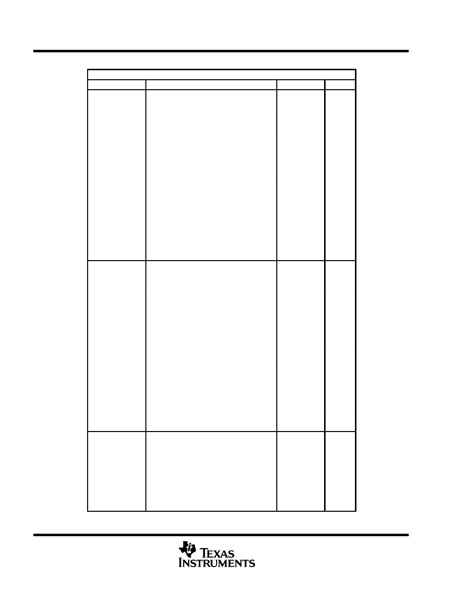
MSP430x13x, MSP430x14x
MIXED SIGNAL MICROCONTROLLER
SLAS272C – JULY 2000 – REVISED FEBRUARY 2001
34
POST OFFICE BOX 655303
•
DALLAS, TEXAS 75265
peripheral file map
PERIPHERALS WITH WORD ACCESS
Watchdog
Watchdog Timer control
WDTCTL
0120h
Timer_B7
Timer_B interrupt vector
TBIV
011Eh
Timer_B3
(see Note 10)
Timer_B control
TBCTL
0180h
(see Note 10)
Capture/compare control 0
CCTL0
0182h
Capture/compare control 1
CCTL1
0184h
Capture/compare control 2
CCTL2
0186h
Capture/compare control 3
CCTL3
0188h
Capture/compare control 4
CCTL4
018Ah
Capture/compare control 5
CCTL5
018Ch
Capture/compare control 6
CCTL6
018Eh
Timer_B register
TBR
0190h
Capture/compare register 0
CCR0
0192h
Capture/compare register 1
CCR1
0194h
Capture/compare register 2
CCR2
0196h
Capture/compare register 3
CCR3
0198h
Capture/compare register 4
CCR4
019Ah
Capture/compare register 5
CCR5
019Ch
Capture/compare register 6
CCR6
019Eh
Timer_A3
Timer_A interrupt vector
TAIV
012Eh
Timer_A control
TACTL
0160h
Capture/compare control 0
CCTL0
0162h
Capture/compare control 1
CCTL1
0164h
Capture/compare control 2
CCTL2
0166h
Reserved
0168h
Reserved
016Ah
Reserved
016Ch
Reserved
016Eh
Timer_A register
TAR
0170h
Capture/compare register 0
CCR0
0172h
Capture/compare register 1
CCR1
0174h
Capture/compare register 2
CCR2
0176h
Reserved
0178h
Reserved
017Ah
Reserved
017Ch
Reserved
017Eh
Multiply
Sum extend
SumExt
013Eh
In MSP430x14x
only
Result high word
ResHi
013Ch
only
Result low word
ResLo
013Ah
Second operand
OP_2
0138h
Multiply signed +accumulate/operand1
MACS
0136h
Multiply+accumulate/operand1
MAC
0134h
Multiply signed/operand1
MPYS
0132h
Multiply unsigned/operand1
MPY
0130h
NOTE 10: Timer_B7 in MSP430x14x family has 7 CCR, Timer_B3 in MSP430x13x family has 3 CCR.
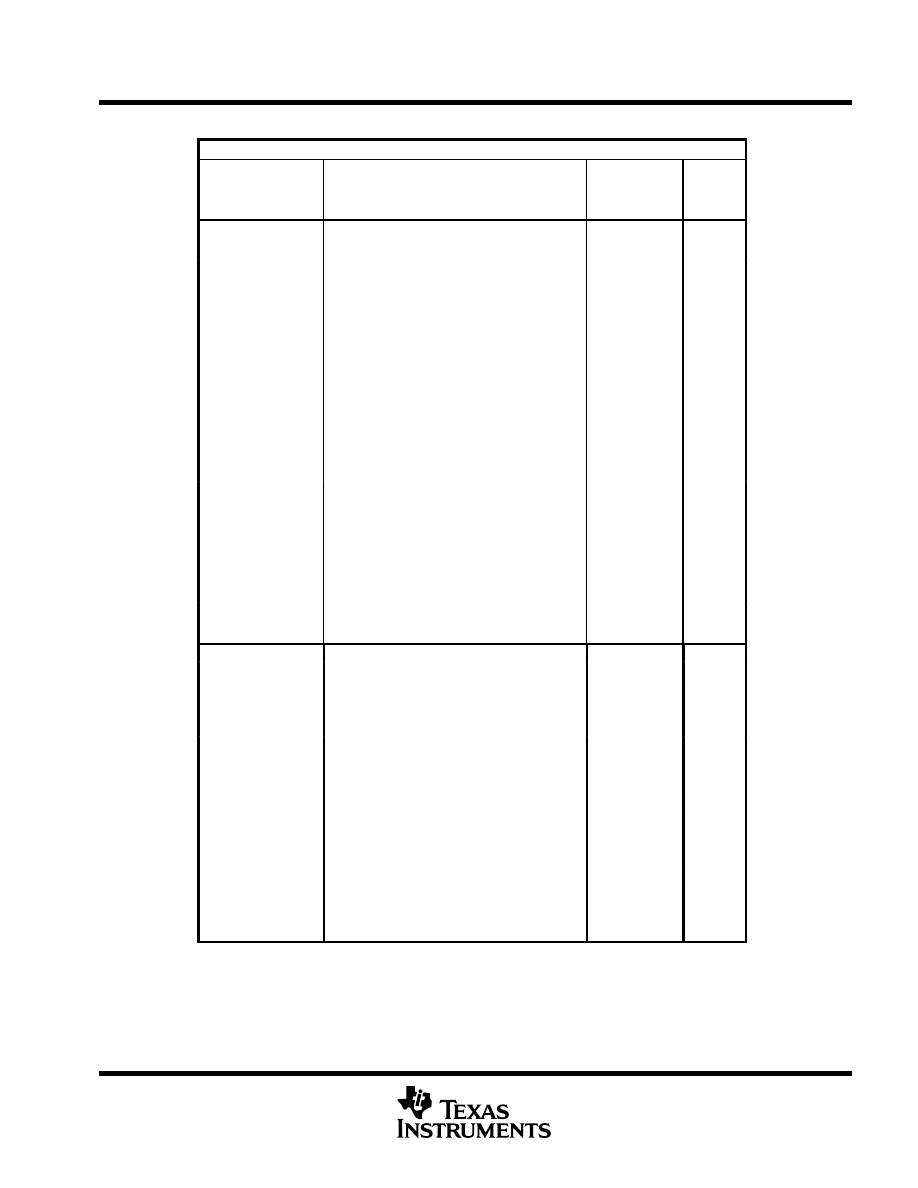
MSP430x13x, MSP430x14x
MIXED SIGNAL MICROCONTROLLER
SLAS272C – JULY 2000 – REVISED FEBRUARY 2001
35
POST OFFICE BOX 655303
•
DALLAS, TEXAS 75265
peripheral file map (continued)
PERIPHERALS WITH WORD ACCESS (CONTINUED)
Flash
Flash control 3
FCTL3
012Ch
Flash control 2
FCTL2
012Ah
Flash control 1
FCTL1
0128h
ADC12
Conversion memory 15
ADC12MEM15
015Eh
See also Peripherals
Conversion memory 14
ADC12MEM14
015Ch
with Byte Access
Conversion memory 13
ADC12MEM13
015Ah
Conversion memory 12
ADC12MEM12
0158h
Conversion memory 11
ADC12MEM11
0156h
Conversion memory 10
ADC12MEM10
0154h
Conversion memory 9
ADC12MEM9
0152h
Conversion memory 8
ADC12MEM8
0150h
Conversion memory 7
ADC12MEM7
014Eh
Conversion memory 6
ADC12MEM6
014Ch
Conversion memory 5
ADC12MEM5
014Ah
Conversion memory 4
ADC12MEM4
0148h
Conversion memory 3
ADC12MEM3
0146h
Conversion memory 2
ADC12MEM2
0144h
Conversion memory 1
ADC12MEM1
0142h
Conversion memory 0
ADC12MEM0
0140h
Interrupt-vector-word register
ADC12IV
01A8h
Inerrupt-enable register
ADC12IE
01A6h
Inerrupt-flag register
ADC12IFG
01A4h
Control register 1
ADC12CTL1
01A2h
Control register 0
ADC12CTL0
01A0h
ADC12
ADC memory-control register15
ADC12MCTL15
08Fh
ADC memory-control register14
ADC12MCTL14
08Eh
ADC memory-control register13
ADC12MCTL13
08Dh
ADC memory-control register12
ADC12MCTL12
08Ch
ADC memory-control register11
ADC12MCTL11
08Bh
ADC memory-control register10
ADC12MCTL10
08Ah
ADC memory-control register9
ADC12MCTL9
089h
ADC memory-control register8
ADC12MCTL8
088h
ADC memory-control register7
ADC12MCTL7
087h
ADC memory-control register6
ADC12MCTL6
086h
ADC memory-control register5
ADC12MCTL5
085h
ADC memory-control register4
ADC12MCTL4
084h
ADC memory-control register3
ADC12MCTL3
083h
ADC memory-control register2
ADC12MCTL2
082h
ADC memory-control register1
ADC12MCTL1
081h
ADC memory-control register0
ADC12MCTL0
080h
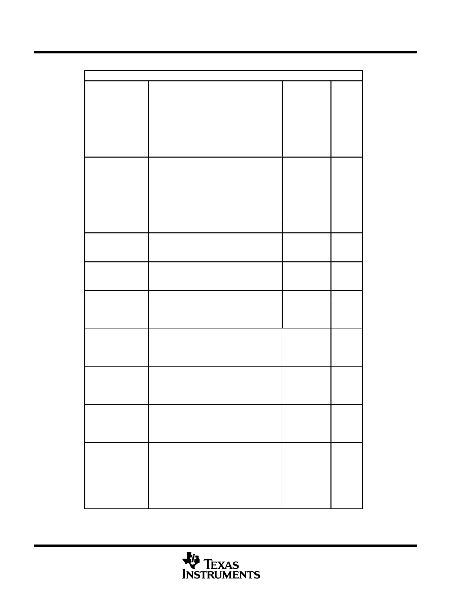
MSP430x13x, MSP430x14x
MIXED SIGNAL MICROCONTROLLER
SLAS272C – JULY 2000 – REVISED FEBRUARY 2001
36
POST OFFICE BOX 655303
•
DALLAS, TEXAS 75265
peripheral file map (continued)
PERIPHERALS WITH BYTE ACCESS
UART1
Transmit buffer
UTXBUF.1
07Fh
(Only in ‘x14x)
Receive buffer
URXBUF.1
07Eh
Baud rate
UBR1.1
07Dh
Baud rate
UBR0.1
07Ch
Modulation control
UMCTL.1
07Bh
Receive control
URCTL.1
07Ah
Transmit control
UTCTL.1
079h
UART control
UCTL.1
078h
UART0
Transmit buffer
UTXBUF.0
077h
Receive buffer
URXBUF.0
076h
Baud rate
UBR1.0
075h
Baud rate
UBR0.0
074h
Modulation control
UMCTL.0
073h
Receive control
URCTL.0
072h
Transmit control
UTCTL.0
071h
UART control
UCTL.0
070h
Comparator_A
Comp._A port disable
CAPD
05Bh
Comp._A control2
CACTL2
05Ah
Comp._A control1
CACTL1
059h
System Clock
Basic clock system control2
BCSCTL2
058h
Basic clock system control1
BCSCTL1
057h
DCO clock frequency control
DCOCTL
056h
Port P6
Port P6 selection
P6SEL
037h
Port P6 direction
P6DIR
036h
Port P6 output
P6OUT
035h
Port P6 input
P6IN
034h
Port P5
Port P5 selection
P5SEL
033h
Port P5 direction
P5DIR
032h
Port P5 output
P5OUT
031h
Port P5 input
P5IN
030h
Port P4
Port P4 selection
P4SEL
01Fh
Port P4 direction
P4DIR
01Eh
Port P4 output
P4OUT
01Dh
Port P4 input
P4IN
01Ch
Port P3
Port P3 selection
P3SEL
01Bh
Port P3 direction
P3DIR
01Ah
Port P3 output
P3OUT
019h
Port P3 input
P3IN
018h
Port P2
Port P2 selection
P2SEL
02Eh
Port P2 interrupt enable
P2IE
02Dh
Port P2 interrupt-edge select
P2IES
02Ch
Port P2 interrupt flag
P2IFG
02Bh
Port P2 direction
P2DIR
02Ah
Port P2 output
P2OUT
029h
Port P2 input
P2IN
028h

MSP430x13x, MSP430x14x
MIXED SIGNAL MICROCONTROLLER
SLAS272C – JULY 2000 – REVISED FEBRUARY 2001
37
POST OFFICE BOX 655303
•
DALLAS, TEXAS 75265
peripheral file map (continued)
PERIPHERALS WITH BYTE ACCESS
Port P1
Port P1 selection
P1SEL
026h
Port P1 interrupt enable
P1IE
025h
Port P1 interrupt-edge select
P1IES
024h
Port P1 interrupt flag
P1IFG
023h
Port P1 direction
P1DIR
022h
Port P1 output
P1OUT
021h
Port P1 input
P1IN
020h
Special Functions
SFR module enable 2
ME2
005h
SFR module enable 1
ME1
004h
SFR interrupt flag2
IFG2
003h
SFR interrupt flag1
IFG1
002h
SFR interrupt enable2
IE2
001h
SFR interrupt enable1
IE1
000h
absolute maximum ratings over operating free-air temperature (unless otherwise noted)
†
Voltage applied at V
CC
to V
SS
–0.3 V to + 4.1 V
. . . . . . . . . . . . . . . . . . . . . . . . . . . . . . . . . . . . . . . . . . . . . . . . . . . .
Voltage applied to any pin (referenced to V
SS
)
–0.3 V to V
CC
+0.3 V
. . . . . . . . . . . . . . . . . . . . . . . . . . . . . . . . . . .
Diode current at any device terminal .
±
2 mA
. . . . . . . . . . . . . . . . . . . . . . . . . . . . . . . . . . . . . . . . . . . . . . . . . . . . . .
Storage temperature (unprogrammed device)
– 55
°
C to 150
°
C
. . . . . . . . . . . . . . . . . . . . . . . . . . . . . . . . . . . . . . .
Storage temperature (programmed device)
– 40
°
C to 85
°
C
. . . . . . . . . . . . . . . . . . . . . . . . . . . . . . . . . . . . . . . . . .
† Stresses beyond those listed under “absolute maximum ratings” may cause permanent damage to the device. These are stress ratings only, and
functional operation of the device at these or any other conditions beyond those indicated under “recommended operating conditions” is not
implied. Exposure to absolute-maximum-rated conditions for extended periods may affect device reliability.
NOTE: All voltages referenced to VSS.
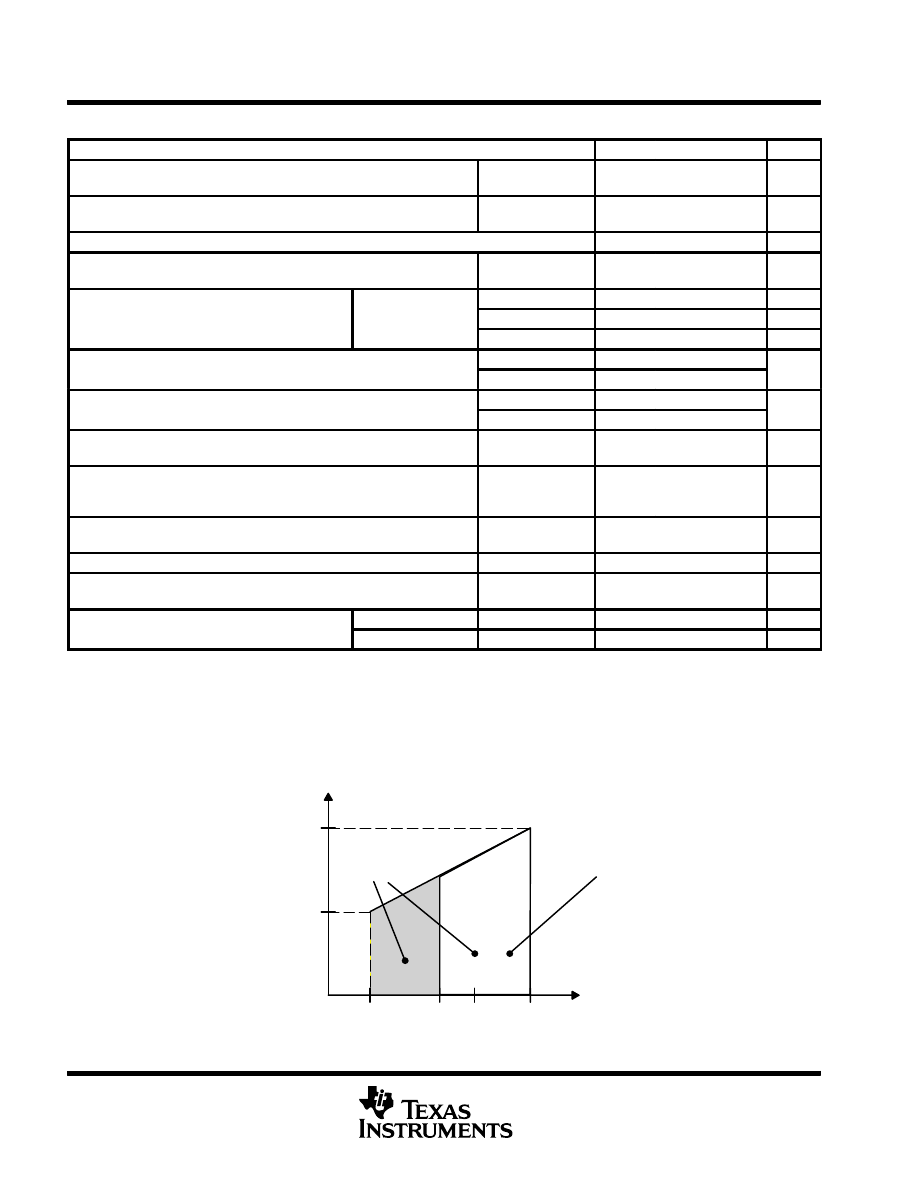
MSP430x13x, MSP430x14x
MIXED SIGNAL MICROCONTROLLER
SLAS272C – JULY 2000 – REVISED FEBRUARY 2001
38
POST OFFICE BOX 655303
•
DALLAS, TEXAS 75265
recommended operating conditions
PARAMETER
MIN
NOM
MAX
UNITS
Supply voltage during program execution, VCC (AVCC = DVCC = VCC)
MSP430F13x,
MSP430F14x
1.8
3.6
V
Supply voltage during flash memory programming, VCC
(AVCC = DVCC = VCC)
MSP430F13x,
MSP430F14x
2.7
3.6
V
Supply voltage, VSS
0.0
0.0
V
Operating free-air temperature range, TA
MSP430x13x
MSP430x14x
–40
85
°
C
LFXT1
t l f
f
LF selected, XTS=0
Watch crystal
32768
Hz
LFXT1 crystal frequency, f(LFXT1)
(see Notes 10 and 11)
XT1 selected, XTS=1
Ceramic resonator
450
8000
kHz
(see Notes 10 and 11)
XT1 selected, XTS=1
Crystal
1000
8000
kHz
XT2 crystal frequency f(XT2)
Ceramic resonator
450
8000
kHz
XT2 crystal frequency, f(XT2)
Crystal
1000
8000
kHz
Processor frequency (signal MCLK) f(S t
)
VCC = 1.8 V
DC
4.15
MHz
Processor frequency (signal MCLK), f(System)
VCC = 3.6 V
DC
8
MHz
Flash-timing-generator frequency, f(FTG)
MSP430F13x,
MSP430F14x
257
476
kHz
Cumulative program time, t(CPT) (see Note 13)
VCC = 2.7 V/3.6 V
MSP430F13x
MSP430F14x
3
ms
Mass erase time, t(MEras) (See also the flash memory, timing generator,
control register FCTL2 section, see Note 14)
VCC = 2.7 V/3.6 V
200
ms
Low-level input voltage (TCK, TMS, TDI, RST/NMI), VIL (excluding Xin, Xout) VCC = 2.2 V/3 V
VSS
VSS +0.6
V
High-level input voltage (TCK, TMS, TDI, RST/NMI), VIH
(excluding Xin, Xout)
VCC = 2.2 V/3 V
0.8VCC
VCC
V
Input levels at Xin and Xout
VIL(Xin, Xout)
VCC = 2.2 V/3 V
VSS
0.2
×
VSS
V
Input levels at Xin and Xout
VIH(Xin, Xout)
0.8
×
VCC
VCC
NOTES: 11. In LF mode, the LFXT1 oscillator requires a watch crystal and the LFXT1 oscillator requires a 5.1-M
Ω
resistor from XOUT to VSS
when VCC < 2.5 V. In XT1 mode, the LFXT1. and XT2 oscillators accept a ceramic resonator or a 4-MHz crystal frequency at
VCC
≥
2.2 V. In XT1 mode, the LFXT1 and XT2 oscillators accept a ceramic resonator or an 8-MHz crystal frequency at VCC
≥
2.8 V.
12. In LF mode, the LFXT1 oscillator requires a watch crystal. In XT1 mode, FXT1 accepts a ceramic resonator or a crystal.
13. The cumulative program time must not be exceeded during a segment-write operation. This parameter is only relevant if segment
write option is used.
14. The mass erase duration generated by the flash timing generator is at least 11.1 ms. The cummulative mass erase time needed
is 200 ms. This can be achieved by repeating the mass erase operation until the cumulative mass erase time is met (a minimum
of 19 cycles may be required).
f (MHz)
1.8 V
3.6 V
2.7 V 3 V
ÎÎÎÎÎ
ÎÎÎÎÎ
ÎÎÎÎÎ
ÎÎÎÎÎ
ÎÎÎÎÎ
ÎÎÎÎÎ
ÎÎÎÎÎ
ÎÎÎÎÎ
ÎÎÎÎÎ
4.15 MHz
8.0 MHz
Supply Voltage – V
Supply voltage range, ’F13x/’F14x,
during flash memory programming
Supply voltage range,
’F13x/’F14x, during
program execution
Figure 3. Frequency vs Supply Voltage, MSP430F13x or MSP430F14x
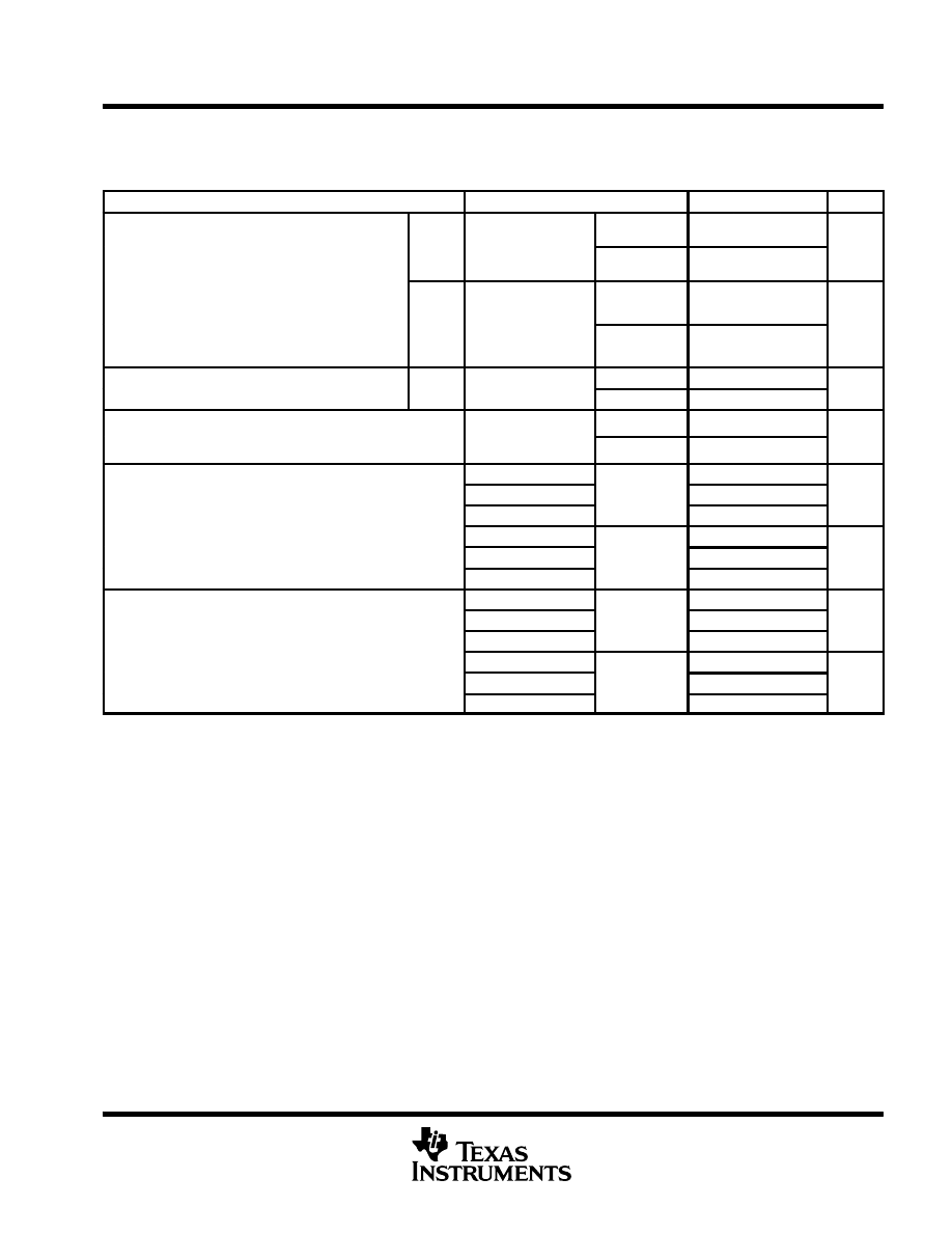
MSP430x13x, MSP430x14x
MIXED SIGNAL MICROCONTROLLER
SLAS272C – JULY 2000 – REVISED FEBRUARY 2001
39
POST OFFICE BOX 655303
•
DALLAS, TEXAS 75265
electrical characteristics over recommended operating free-air temperature (unless otherwise
noted)
supply current into AV
CC
+ DV
CC
excluding external current, f
(System)
= 1 MHz
PARAMETER
TEST CONDITIONS
MIN
NOM
MAX
UNIT
I(AM)
Active mode, (see Note 15)
f(MCLK) = f(SMCLK) = 1 MHz,
F13x,
TA = 40
°
C to 85
°
C
VCC = 2.2 V
280
350
µ
A
I(AM)
(MCLK)
(SMCLK)
,
f(ACLK) = 32,768 Hz
XTS=0, SELM=(0,1)
,
F14x
TA = –40
°
C to 85
°
C
VCC = 3 V
420
560
µ
A
I(AM)
Active mode, (see Note 15)
f(MCLK) = f(SMCLK) = 4 096 Hz,
f(ACLK) = 4 096 Hz
F13x,
TA = 40
°
C to 85
°
C
VCC = 2.2 V
2.5
7
µ
A
I(AM)
f(ACLK) = 4,096 Hz
XTS=0, SELM=(0,1)
XTS=0, SELM=3
,
F14x
TA = –40
°
C to 85
°
C
VCC = 3 V
9
20
µ
A
I(LPM0)
Low-power mode, (LPM0)
F13x,
TA = 40
°
C to 85
°
C
VCC = 2.2 V
32
45
µ
A
I(LPM0)
, (
)
(see Note 15)
,
F14x
TA = –40
°
C to 85
°
C
VCC = 3 V
55
70
µ
A
I(LPM2)
Low-power mode, (LPM2),
f(MCLK)
f (SMCLK)
0 MHz
TA = 40
°
C to 85
°
C
VCC = 2.2 V
11
14
µ
A
I(LPM2)
f(MCLK) = f (SMCLK) = 0 MHz,
f(ACLK) = 32.768 Hz, SCG0 = 0
TA = –40
°
C to 85
°
C
VCC = 3 V
17
22
µ
A
TA = –40
°
C
0.8
1.5
TA = 25
°
C
VCC = 2.2 V
0.9
1.5
µ
A
I(LPM3)
Low-power mode, (LPM3)
f(MCLK) f(SMCLK) 0 MHz
TA = 85
°
C
1.6
2.8
I(LPM3)
f(MCLK) = f(SMCLK) = 0 MHz,
f(ACLK) = 32,768 Hz, SCG0 = 1 (see Note 16)
TA = –40
°
C
1.8
2.2
f(ACLK) = 32,768 Hz, SCG0 = 1 (see Note 16)
TA = 25
°
C
VCC = 3 V
1.6
1.9
µ
A
TA = 85
°
C
2.3
3.9
TA = –40
°
C
0.1
0.5
TA = 25
°
C
VCC = 2.2 V
0.1
0.5
µ
A
I(LPM4)
Low-power mode, (LPM4)
f(MCLK) 0 MHz
f(SMCLK) 0 MHz
TA = 85
°
C
0.8
2.5
I(LPM4)
f(MCLK) = 0 MHz, f(SMCLK) = 0 MHz,
f(ACLK) = 0 Hz, SCG0 = 1
TA = –40
°
C
0.1
0.5
f(ACLK) = 0 Hz, SCG0 = 1
TA = 25
°
C
VCC = 3 V
0.1
0.5
µ
A
TA = 85
°
C
0.8
2.5
NOTES: 15. Timer_B is clocked by f(DCOCLK) = 1 MHz. All inputs are tied to 0 V or to VCC. Outputs do not source or sink any current.
16. Timer_B is clocked by f(ACLK) = 32,768 Hz. All inputs are tied to 0 V or to VCC. Outputs do not source or sink any current. The current
consumption in LPM2 and LPM3 are measured with ACLK selected.
MSP430x13x, MSP430x14x
MIXED SIGNAL MICROCONTROLLER
SLAS272C – JULY 2000 – REVISED FEBRUARY 2001
40
POST OFFICE BOX 655303
•
DALLAS, TEXAS 75265
electrical characteristics over recommended operating free-air temperature (unless otherwise
noted) (continued)
Current consumption of active mode versus system frequency, F-version
I(AM) = I(AM) [1 MHz]
×
f(System) [MHz]
Current consumption of active mode versus supply voltage, F-version
I
(AM)
= I
(AM) [3 V]
+ 175
µ
A/V
×
(V
CC
– 3 V)
SCHMITT-trigger inputs – Ports P1, P2, P3, P4, P5, and P6
PARAMETER
TEST CONDITIONS
MIN
TYP
MAX
UNIT
VIT
Positive going input threshold voltage
VCC = 2.2 V
1.1
1.5
V
VIT+
Positive-going input threshold voltage
VCC = 3 V
1.5
1.9
V
VIT
Negative going input threshold voltage
VCC = 2.2 V
0.4
0.9
V
VIT–
Negative-going input threshold voltage
VCC = 3 V
0.90
1.3
V
Vh
Input voltage hysteresis (VIT
VIT )
VCC = 2.2 V
0.3
1.1
V
Vhys
Input voltage hysteresis (VIT+ – VIT–)
VCC = 3 V
0.5
1
V
standard inputs – RST/NMI; JTAG: TCK, TMS, TDI, TDO/TDI
PARAMETER
TEST CONDITIONS
MIN
TYP
MAX
UNIT
VIL
Low-level input voltage
VCC = 2 2 V / 3 V
VSS
VSS+0.6
V
VIH
High-level input voltage
VCC = 2.2 V / 3 V
0.8
×
VCC
VCC
V
outputs – Ports P1, P2, P3, P4, P5, and P6
PARAMETER
TEST CONDITIONS
MIN
TYP
MAX
UNIT
IOH(max) = –1 mA,
VCC = 2.2 V,
See Note 17
VCC–0.25
VCC
VOH
High level output voltage
IOH(max) = –3.4 mA, VCC = 2.2 V,
See Note 18
VCC–0.6
VCC
V
VOH
High-level output voltage
IOH(max) = –1 mA,
VCC = 3 V,
See Note 17
VCC–0.25
VCC
V
IOH(max) = –3.4 mA, VCC = 3 V,
See Note 18
VCC–0.6
VCC
IOL(max) = 1.5 mA,
VCC = 2.2 V,
See Note 17
VSS
VSS+0.25
VOL
Low level output voltage
IOL(max) = 6 mA,
VCC = 2.2 V,
See Note 18
VSS
VSS+0.6
V
VOL
Low-level output voltage
IOL(max) = 1.5 mA,
VCC = 3 V,
See Note 17
VSS
VSS+0.25
V
IOL(max) = 6 mA,
VCC = 3 V,
See Note 18
VSS
VSS+0.6
NOTES: 17. The maximum total current, IOH(max) and IOL(max), for all outputs combined, should not exceed
±
6 mA to satisfy the maximum
specified voltage drop.
18. The maximum total current, IOH(max) and IOL(max), for all outputs combined, should not exceed
±
24 mA to satisfy the maximum
specified voltage drop.
MSP430x13x, MSP430x14x
MIXED SIGNAL MICROCONTROLLER
SLAS272C – JULY 2000 – REVISED FEBRUARY 2001
41
POST OFFICE BOX 655303
•
DALLAS, TEXAS 75265
outputs – Ports P1, P2, P3, P4, P5, and P6 (continued)
Figure 4
VOL – Low-Level Output Voltage – V
0
2
4
6
8
10
12
14
16
0
0.5
1.0
1.5
2.0
2.5
VCC = 2.2 V
P2.7
TYPICAL LOW-LEVEL OUTPUT CURRENT
vs
LOW-LEVEL OUTPUT VOLTAGE
TA = 25
°
C
TA = 85
°
C
OLI
–
Low-Level Output Current
–
mA
Figure 5
VOL – Low-Level Output Voltage – V
0
5
10
15
20
25
0
0.5
1.0
1.5
2.0
2.5
3.0
3.5
VCC = 3 V
P2.7
TYPICAL LOW-LEVEL OUTPUT CURRENT
vs
LOW-LEVEL OUTPUT VOLTAGE
TA = 25
°
C
TA = 85
°
C
OLI
–
Low-Level Output Current
–
mA
Figure 6
VOH – High-Level Output Voltage – V
–14
–12
–10
–8
–6
–4
–2
0
0
0.5
1.0
1.5
2.0
2.5
VCC = 2.2 V
P2.7
TYPICAL HIGH-LEVEL OUTPUT CURRENT
vs
HIGH-LEVEL OUTPUT VOLTAGE
TA = 25
°
C
TA = 85
°
C
OHI
–
High-Level Output Current
–
mA
Figure 7
VOH – High-Level Output Voltage – V
–30
–25
–20
–15
–10
–5
0
0
0.5
1.0
1.5
2.0
2.5
3.0
3.5
VCC = 3 V
P2.7
TYPICAL HIGH-LEVEL OUTPUT CURRENT
vs
HIGH-LEVEL OUTPUT VOLTAGE
TA = 25
°
C
TA = 85
°
C
OHI
–
High-Level Output Current
–
mA
MSP430x13x, MSP430x14x
MIXED SIGNAL MICROCONTROLLER
SLAS272C – JULY 2000 – REVISED FEBRUARY 2001
42
POST OFFICE BOX 655303
•
DALLAS, TEXAS 75265
electrical characteristics over recommended operating free-air temperature (unless otherwise
noted) (continued)
input frequency – Ports P1, P2, P3, P4, P5, and P6
PARAMETER
TEST CONDITIONS
MIN
TYP
MAX
UNIT
f(IN)
t(h) = t(L)
VCC = 2.2 V
8
MHz
t(h) = t(L)
VCC = 3 V
10
MHz
capture timing _ Timer_A3: TA0, TA1, TA2; Timer_B7: TB0 to TB6
PARAMETER
TEST CONDITIONS
MIN
TYP
MAX
UNIT
P t P2 P4
VCC = 2.2 V/3 V
1.5
Cycle
t(int)
Ports P2, P4:
External trigger signal for the interrupt flag (see Notes 19 and 20)
VCC = 2.2 V
62
ns
(
)
External trigger signal for the interru t flag (see Notes 19 and 20)
VCC = 3 V
50
ns
NOTES: 19. The external signal sets the interrupt flag every time t(int) is met. It may be set even with trigger signals shorter than t(int).
The conditions to set the flag must be met independently of this timing constraint. t(int) is defined in MCLK cycles.
20. The external signal needs additional timing because of the maximum input-frequency constraint.
output frequency
PARAMETER
TEST CONDITIONS
MIN
TYP
MAX
UNIT
fTAx
TA0..2, TB0–TB6,
Internal clock source, SMCLK signal
applied (see Note 21)
CL = 20 pF
DC
fSystem
MHz
fACLK,
fMCLK,
fSMCLK
P5.6/ACLK, P5.4/MCLK, P5.5/SMCLK
CL = 20 pF
fSystem
MHz
P2.0/ACLK
fACLK = fLFXT1 = fXT1
40%
60%
P2.0/ACLK
CL = 20 pF,
fACLK = fLFXT1 = fLF
30%
70%
VCC = 2.2 V / 3 V fACLK = fLFXT1/n
50%
fSMCLK = fLFXT1 = fXT1
40%
60%
tXdc
Duty cycle of output frequency,
P1 4/SMCLK
fSMCLK = fLFXT1 = fLF
35%
65%
P1.4/SMCLK,
CL = 20 pF,
VCC = 2.2 V / 3 V
fSMCLK = fLFXT1/n
50%–
15 ns
50%
50%–
15 ns
VCC = 2.2 V / 3 V
fSMCLK = fDCOCLK
50%–
15 ns
50%
50%–
15 ns
NOTE 21: The limits of the system clock MCLK has to be met; the system (MCLK) frequency should not exceed the limits. MCLK and SMCLK
frequencies can be different.
external interrupt timing
PARAMETER
TEST CONDITIONS
MIN
TYP
MAX
UNIT
P t P1 P2
VCC = 2.2 V/3 V
1.5
Cycle
t(int)
Ports P1, P2:
External trigger signal for the interrupt flag (see Notes 22 and 23)
VCC = 2.2 V
62
ns
(
)
External trigger signal for the interru t flag (see Notes 22 and 23)
VCC = 3 V
50
ns
NOTES: 22. The external signal sets the interrupt flag every time t(int) is met. It may be set even with trigger signals shorter than t(int).
The conditions to set the flag must be met independently of this timing constraint. t(int) is defined in MCLK cycles.
23. The external signal needs additional timing because of the maximum input-frequency constraint.
wake-up LPM3
PARAMETER
TEST CONDITIONS
MIN
TYP
MAX
UNIT
f = 1 MHz
6
t(LPM3) Delay time
f = 2 MHz
VCC = 2.2 V/3 V
6
µ
s
(
)
f = 3 MHz
6
MSP430x13x, MSP430x14x
MIXED SIGNAL MICROCONTROLLER
SLAS272C – JULY 2000 – REVISED FEBRUARY 2001
43
POST OFFICE BOX 655303
•
DALLAS, TEXAS 75265
electrical characteristics over recommended operating free-air temperature (unless otherwise
noted) (continued)
leakage current (see Note 24)
PARAMETER
TEST CONDITIONS
MIN
TYP
MAX
UNIT
Ilkg(P1.x)
L
k
Port P1
Port 1: V(P1.x) (see Note 25)
±
50
Ilkg(P2.x)
Leakage
current
Port P2
Port 2: V(P2.3) V(P2.4) (see Note 25)
VCC = 2.2 V/3 V
±
50
nA
Ilkg(P6.x)
current
Port P6
Port 6: V(P6.x) (see Note 25)
±
50
NOTES: 24. The leakage current is measured with VSS or VCC applied to the corresponding pin(s), unless otherwise noted.
25. The port pin must be selected as input and there must be no optional pullup or pulldown resistor.
RAM
PARAMETER
TEST CONDITIONS
MIN
TYP
MAX
UNIT
VRAMh
CPU HALTED (see Note 26)
1.6
V
NOTE 26: This parameter defines the minimum supply voltage when the data in program memory RAM remain unchanged. No program execution
should take place during this supply voltage condition.
Comparator_A (see Note 27)
PARAMETER
TEST CONDITIONS
MIN
TYP
MAX
UNIT
I(DD)
CAON=1
CARSEL=0
CAREF=0
VCC = 2.2 V
25
40
µ
A
I(DD)
CAON=1, CARSEL=0, CAREF=0
VCC = 3 V
45
60
µ
A
I(R fl dd /R fdi d )
CAON=1, CARSEL=0,
CAREF=1/2/3 no load at
VCC = 2.2 V
30
50
µ
A
I(Refladder/Refdiode)
CAREF=1/2/3, no load at
P2.3/CA0/TA1 and P2.4/CA1/TA2
VCC = 3 V
45
71
µ
A
V(IC)
Common-mode input
voltage
CAON =1
VCC = 2.2 V/3 V
0
VCC–1
V
V(Ref025)
See Figure 8
Voltage @ 0.25 V
CC
node
V
CC
PCA0=1, CARSEL=1, CAREF=1,
no load at P2.3/CA0/TA1 and
P2.4/CA1/TA2, See Figure 8
VCC = 2.2 V/3 V
0.23
0.24
0.25
V(Ref050)
See Figure 8
Voltage @ 0.5 V
CC
node
V
CC
PCA0=1, CARSEL=1, CAREF=2,
no load at P2.3/CA0/TA1 and
P2.4/CA1/TA2, See Figure 8
VCC = 2.2 V/3 V
0.47
0.48
0.5
V(R fVT)
PCA0=1, CARSEL=1, CAREF=3,
no load at P2 3/CA0/TA1 and
VCC = 2.2 V
390
480
540
mV
V(RefVT)
no load at P2.3/CA0/TA1 and
P2.4/CA1/TA2 TA = 85
°
C
VCC = 3 V
400
490
550
mV
V(offset)
Offset voltage
See Note 28
VCC = 2.2 V/3 V
–30
30
mV
Vhys
Input hysteresis
CAON=1
VCC = 2.2 V/3 V
0
0.7
1.4
mV
TA = 25
°
C, Overdrive 10 mV, With-
VCC = 2.2 V
130
210
300
ns
t(
LH)
A
out filter: CAF=0
VCC = 3 V
80
150
240
ns
t(response LH)
TA = 25
°
C, Overdrive 10 mV, With
VCC = 2.2 V
1.4
1.9
3.4
µ
s
A
filter: CAF=1
VCC = 3 V
0.9
1.5
2.6
µ
s
TA = 25
°
C,
Overdrive 10 mV without filter:
VCC = 2.2 V
130
210
300
ns
t(response HL)
Overdrive 10 mV, without filter:
CAF=0
VCC = 3 V
80
150
240
ns
(res onse HL)
TA = 25
°
C,
VCC = 2.2 V
1.4
1.9
3.4
µ
s
A
Overdrive 10 mV, with filter: CAF=1
VCC = 3 V
0.9
1.5
2.6
µ
s
NOTES: 27. The leakage current for the Comparator_A terminals is identical to Ilkg(Px.x) specification.
28. The input offset voltage can be cancelled by using the CAEX bit to invert the Comparator_A inputs on successive measurements.
The two successive measurements are then summed together.
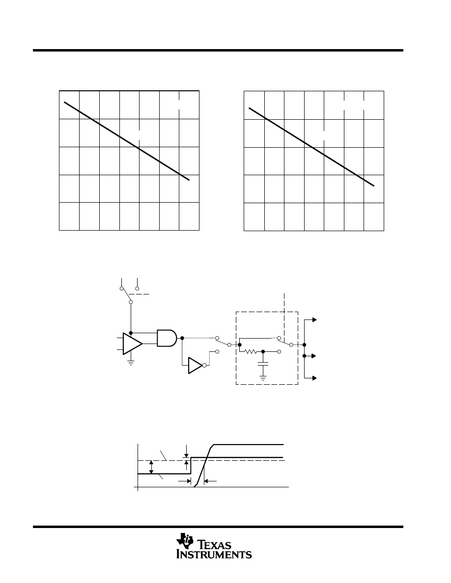
MSP430x13x, MSP430x14x
MIXED SIGNAL MICROCONTROLLER
SLAS272C – JULY 2000 – REVISED FEBRUARY 2001
44
POST OFFICE BOX 655303
•
DALLAS, TEXAS 75265
electrical characteristics over recommended operating free-air temperature (unless otherwise
noted) (continued)
TA – Free-Air Temperature –
°
C
400
450
500
550
600
650
–45
–25
–5
15
35
55
75
95
VCC = 3 V
Figure 8. V
(RefVT)
vs Temperature, V
CC
= 3 V
V
(REFVT)
–
Reference V
olts
–
mV
Typical
Figure 9. V
(RefVT)
vs Temperature, V
CC
= 2.2 V
TA – Free-Air Temperature –
°
C
400
450
500
550
600
650
–45
–25
–5
15
35
55
75
95
VCC = 2.2 V
V
(REFVT)
–
Reference V
olts
–
mV
Typical
_
+
CAON
0
1
V+
0
1
CAF
Low Pass Filter
τ
≈
2.0
µ
s
To Internal
Modules
Set CAIFG
Flag
CAOUT
V–
VCC
1
0 V
0
Figure 10. Block Diagram of Comparator_A Module
Overdrive
VCAOUT
t(response)
V+
V–
400 mV
Figure 11. Overdrive Definition
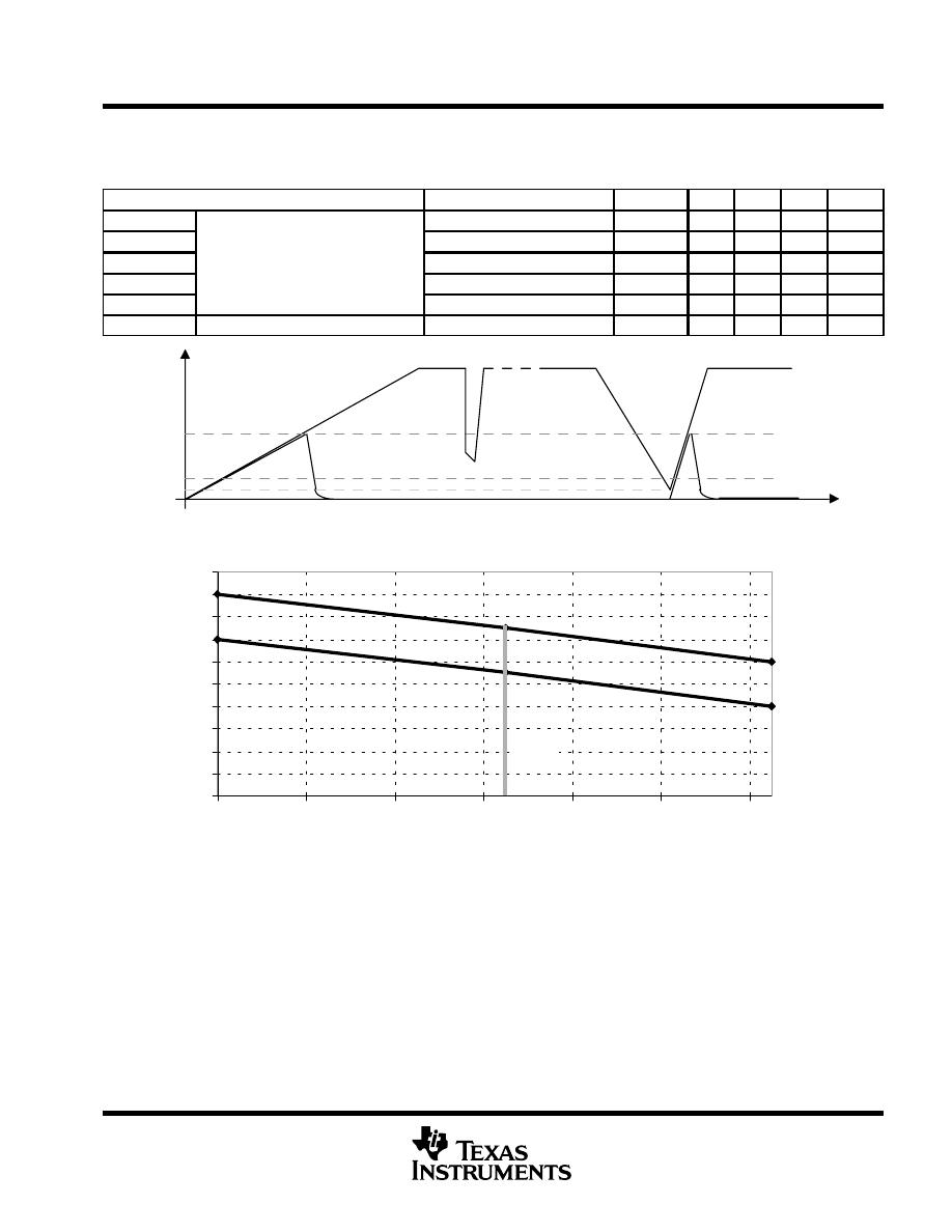
MSP430x13x, MSP430x14x
MIXED SIGNAL MICROCONTROLLER
SLAS272C – JULY 2000 – REVISED FEBRUARY 2001
45
POST OFFICE BOX 655303
•
DALLAS, TEXAS 75265
electrical characteristics over recommended operating free-air temperature (unless otherwise
noted) (continued)
POR
PARAMETER
CONDITIONS
VCC
MIN
NOM
MAX
UNIT
t(POR) Delay
2.2 V/3 V
150
250
µ
s
V(POR)
TA = –40
°
C
1.4
1.8
V
V(POR)
POR
TA = +25
°
C
1.1
1.5
V
V(POR)
TA = +85
°
C
0.8
1.2
V
V(min)
0
0.4
V
t(Reset)
PUC/POR
Reset is accepted internally
2.2 V/3 V
2
µ
s
VCC
POR
V
t
V
(POR)
V
(min)
POR
No POR
Figure 12. Power-On Reset (POR) vs Supply Voltage
1.2
1.5
1.8
0.8
1.2
1.4
0
0.2
0.4
0.6
0.8
1
1.2
1.4
1.6
1.8
2
–40
–20
0
20
40
60
80
25
°
C
TA – Temperature –
°
C
V
(POR)
–
V
Figure 13. V(POR) vs Temperature
MSP430x13x, MSP430x14x
MIXED SIGNAL MICROCONTROLLER
SLAS272C – JULY 2000 – REVISED FEBRUARY 2001
46
POST OFFICE BOX 655303
•
DALLAS, TEXAS 75265
electrical characteristics over recommended operating free-air temperature (unless otherwise
noted) (continued)
DCO (see Note 29)
PARAMETER
TEST CONDITIONS
MIN
NOM
MAX
UNIT
f(DCO03)
Rsel = 0, DCO = 3, MOD = 0, DCOR = 0, TA = 25
°
C
VCC = 2.2 V
0.08
0.12
0.15
MHz
f(DCO03)
VCC = 3 V
0.08
0.13
0.16
MHz
f(DCO13)
Rsel = 1, DCO = 3, MOD = 0, DCOR = 0, TA = 25
°
C
VCC = 2.2 V
0.14
0.19
0.23
MHz
f(DCO13)
VCC = 3 V
0.14
0.18
0.22
MHz
f(DCO23)
Rsel = 2, DCO = 3, MOD = 0, DCOR = 0, TA = 25
°
C
VCC = 2.2 V
0.22
0.30
0.36
MHz
f(DCO23)
VCC = 3 V
0.22
0.28
0.34
MHz
f(DCO33)
Rsel = 3, DCO = 3, MOD = 0, DCOR = 0, TA = 25
°
C
VCC = 2.2 V
0.37
0.49
0.59
MHz
f(DCO33)
VCC = 3 V
0.37
0.47
0.56
MHz
f(DCO43)
Rsel = 4, DCO = 3, MOD = 0, DCOR = 0, TA = 25
°
C
VCC = 2.2 V
0.61
0.77
0.93
MHz
f(DCO43)
VCC = 3 V
0.61
0.75
0.90
MHz
f(DCO53)
Rsel = 5, DCO = 3, MOD = 0, DCOR = 0, TA = 25
°
C
VCC = 2.2 V
1
1.2
1.5
MHz
f(DCO53)
VCC = 3 V
1
1.3
1.5
MHz
f(DCO63)
Rsel = 6, DCO = 3, MOD = 0, DCOR = 0, TA = 25
°
C
VCC = 2.2 V
1.6
1.9
2.2
MHz
f(DCO63)
VCC = 3 V
1.69
2.0
2.29
MHz
f(DCO73)
Rsel = 7, DCO = 3, MOD = 0, DCOR = 0, TA = 25
°
C
VCC = 2.2 V
2.4
2.9
3.4
MHz
f(DCO73)
VCC = 3 V
2.7
3.2
3.65
MHz
f(DCO47)
Rsel = 4, DCO = 7, MOD = 0, DCOR = 0, TA = 25
°
C
VCC = 2.2 V/3 V
fDCO40
×
1.7
fDCO40
×
2.1
fDCO40
×
2.5
MHz
f(DCO77)
R
l = 7 DCO = 7 MOD = 0 DCOR = 0 TA = 25
°
C
VCC = 2.2 V
4
4.5
4.9
MHz
f(DCO77)
Rsel = 7, DCO = 7, MOD = 0, DCOR = 0, TA = 25
°
C
VCC = 3 V
4.4
4.9
5.4
MHz
S(Rsel)
SR = fRsel+1 / fRsel
VCC = 2.2 V/3 V
1.35
1.65
2
S(DCO)
SDCO = fDCO+1 / fDCO
VCC = 2.2 V/3 V
1.07
1.12
1.16
Dt
Temperature drift, Rsel = 4, DCO = 3, MOD = 0
VCC = 2.2 V
–0.31
–0.36
–0.40
%/
°
C
Dt
,
sel
,
,
(see Note 30)
VCC = 3 V
–0.33
–0.38
–0.43
%/
°
C
DV
Drift with VCC variation, Rsel = 4, DCO = 3, MOD = 0
(see Note 30)
VCC = 2.2 V/3 V
0
5
10
%/V
NOTES: 29. The DCO frequency may not exceed the maximum system frequency defined by parameter processor frequency, f(System).
30. This parameter is not production tested.
3
5
f DCO_0
max.
min.
ÎÎÎÎÎÎÎ
ÎÎÎÎÎÎÎ
max.
min.
f DCO_7
DCO
0
1
2
3
4
5
6
7
f DCOCLK
1
ÎÎÎÎÎÎÎ
ÎÎÎÎÎÎÎ
VCC – V
Figure 14. DCO Characteristics
MSP430x13x, MSP430x14x
MIXED SIGNAL MICROCONTROLLER
SLAS272C – JULY 2000 – REVISED FEBRUARY 2001
47
POST OFFICE BOX 655303
•
DALLAS, TEXAS 75265
electrical characteristics over recommended operating free-air temperature (unless otherwise
noted) (continued)
main DCO characteristics
D
Individual devices have a minimum and maximum operation frequency. The specified parameters for
f
DCOx0
to f
DCOx7
are valid for all devices.
D
All ranges selected by Rsel(n) overlap with Rsel(n+1): Rsel0 overlaps with Rsel1, ... Rsel6 overlaps with
Rsel7.
D
DCO control bits DCO0, DCO1, and DCO2 have a step size as defined by parameter S
DCO
.
D
Modulation control bits MOD0 to MOD4 select how often f
DCO+1
is used within the period of 32 DCOCLK
cycles. The frequency f
(DCO)
is used for the remaining cycles. The frequency is an average equal to
f(DCO)
×
(2
MOD/32
).
crystal oscillator, LFXT1 oscillator (see Note 31)
PARAMETER
TEST CONDITIONS
MIN
NOM
MAX
UNIT
XCIN
Integrated input capacitance
XTS=0; LF oscillator selected
VCC = 2.2 V/3 V
12
pF
XCIN
Integrated input capacitance
XTS=1; XT1 oscillator selected
VCC = 2.2 V/3 V
2
pF
XCOUT
Integrated output capacitance
XTS=0; LF oscillator selected
VCC = 2.2 V/3 V
12
pF
XCOUT
Integrated output capacitance
XTS=1; XT1 oscillator selected
VCC = 2.2 V/3 V
2
pF
XINL
Input levels at XIN, XOUT
VCC = 2.2 V/3 V
VSS
0.2
×
VCC
V
XINH
VCC = 2.2 V/3 V
0.8
×
VCC
VCC
V
NOTE 31: The oscillator needs capacitors at both terminals, with values specified by the crystal manufacturer.
crystal oscillator, XT2 oscillator (see Note 32)
PARAMETER
TEST CONDITIONS
MIN
NOM
MAX
UNIT
XCIN
Integrated input capacitance
VCC = 2.2 V/3 V
2
pF
XCOUT
Integrated output capacitance
VCC = 2.2 V/3 V
2
pF
XINL
Input levels at XIN, XOUT
VCC = 2.2 V/3 V
VSS
0.2
×
VCC
V
XINH
VCC = 2.2 V/3 V
0.8
×
VCC
VCC
V
NOTE 32: The oscillator needs capacitors at both terminals, with values specified by the crystal manufacturer.
USART0, USART1 (see Note 33)
PARAMETER
TEST CONDITIONS
MIN
NOM
MAX
UNIT
t( )
USART0/1: deglitch time
VCC = 2.2 V
200
430
800
ns
t(
τ
)
USART0/1: deglitch time
VCC = 3 V
150
280
500
ns
NOTE 33: The signal applied to the USART0/1 receive signal/terminal (URXD0/1) should meet the timing requirements of t
(
t) to ensure that the
URXS flip-flop is set. The URXS flip-flop is set with negative pulses meeting the minimum-timing condition of t
(
t). The operating
conditions to set the flag must be met independently from this timing constraint. The deglitch circuitry is active only on negative
transitions on the URXD0/1 line.
MSP430x13x, MSP430x14x
MIXED SIGNAL MICROCONTROLLER
SLAS272C – JULY 2000 – REVISED FEBRUARY 2001
48
POST OFFICE BOX 655303
•
DALLAS, TEXAS 75265
electrical characteristics over recommended operating free-air temperature (unless otherwise
noted) (continued)
12-bit ADC, power supply and input range conditions (see Note 34)
PARAMETER
TEST CONDITIONS
MIN
NOM
MAX
UNIT
AVCC
Analog supply voltage
AVCC and DVCC are connected together
AVSS and DVSS are connected together
V(AVSS) = V(DVSS) = 0 V
2.2
3.6
V
VREF
Positive built-in reference
2_5 V = 1 for 2.5 V built-in reference
2 5 V
0 for 1 5 V built in reference
3 V
2.4
2.5
2.6
V
VREF+
voltage output
2_5 V = 0 for 1.5 V built-in reference
IV(REF+)
≤
I(VREF+)max
2.2 V/3 V
1.44
1.5
1.56
V
IVREF
Load current out of VREF+
2.2 V
0.01
–0.5
mA
IVREF+
REF+
terminal
3 V
–1
mA
†
IV(REF)+ = 500
µ
A +/– 100
µ
A
Analog input voltage 0 75 V;
2.2 V
±
2
LSB
IL(VREF) †
Load-current regulation
Analog input voltage ~0.75 V;
2_5 V = 0
3 V
±
2
IL(VREF)+ †
g
VREF+ terminal
IV(REF)+ = 500
µ
A
±
100
µ
A
Analog input voltage ~1.25 V;
2_5 V = 1
3 V
±
2
LSB
I
(
)
‡
Load current regulation
IV(REF)+ =100
µ
A
→
900
µ
A,
VCC 3 V ax 0 5 x VREF
CVREF =5
µ
F
20
ns
IDL(VREF) +‡
g
VREF+ terminal
VCC=3 V, ax ~0.5 x VREF+
Error of conversion result
≤
1 LSB
CVREF+=5
µ
F
20
ns
VeREF+
Positive external
reference voltage input
VeREF+ > VeREF–/VeREF– (see Note 35)
1.4
VAVCC
V
VREF– /VeREF–
Negative external
reference voltage input
VeREF+ > VeREF–/VeREF– (see Note 36)
0
1.2
V
(VeREF+ –
VREF–/VeREF–)
Differential external
reference voltage input
VeREF+ > VeREF–/VeREF– (see Note 37)
1.4
VAVCC
V
V(P6.x/Ax)
Analog input voltage
range (see Note 38)
All P6.0/A0 to P6.7/A7 terminals. Analog inputs
selected in ADC12MCTLx register and P6Sel.x=1
0
≤
x
≤
7; V(AVSS)
≤
VP6.x/Ax
≤
V(AVCC)
0
VAVCC
V
IADC12
Operating supply current
into AVCC terminal
fADC12CLK = 5.0 MHz
ADC12ON
1 REFON
0
2.2 V
0.65
1.3
mA
IADC12
into AVCC terminal
(see Note 39)
ADC12ON = 1, REFON = 0
SHT0=0, SHT1=0, ADC12DIV=0
3 V
0.8
1.6
mA
IREF+
Operating supply current
into AVCC terminal
(see Note 40)
fADC12CLK = 5.0 MHz
ADC12ON = 0,
REFON = 1, 2_5V = 1
3 V
0.5
0.8
mA
IREF
Operating supply current
fADC12CLK = 5.0 MHz
ADC12ON
0
2.2 V
0.5
0.8
mA
IREF+
g
y
(see Note 40)
ADC12ON = 0,
REFON = 1, 2_5V = 0
3 V
0.5
0.8
mA
† Not production tested, limits characterized
‡ Not production tested, limits verified by design
NOTES: 34. The leakage current is defined in the leakage current table with P6.x/Ax parameter.
35. The accuracy limits the minimum positive external reference voltage. Lower reference voltage levels may be applied with reduced
accuracy requirements.
36. The accuracy limits the maximum negative external reference voltage. Higher reference voltage levels may be applied with reduced
accuracy requirements.
37. The accuracy limits minimum external differential reference voltage. Lower differential reference voltage levels may be applied with
reduced accuracy requirements.
38. The analog input voltage range must be within the selected reference voltage range VR+ to VR– for valid conversion results.
39. The internal reference supply current is not included in current consumption parameter IADC12.
40. The internal reference current is supplied via terminal AVCC. Consumption is independent of the ADC12ON control bit, unless a
conversion is active. The REFON bit enables to settle the built-in reference before starting an A/D conversion.
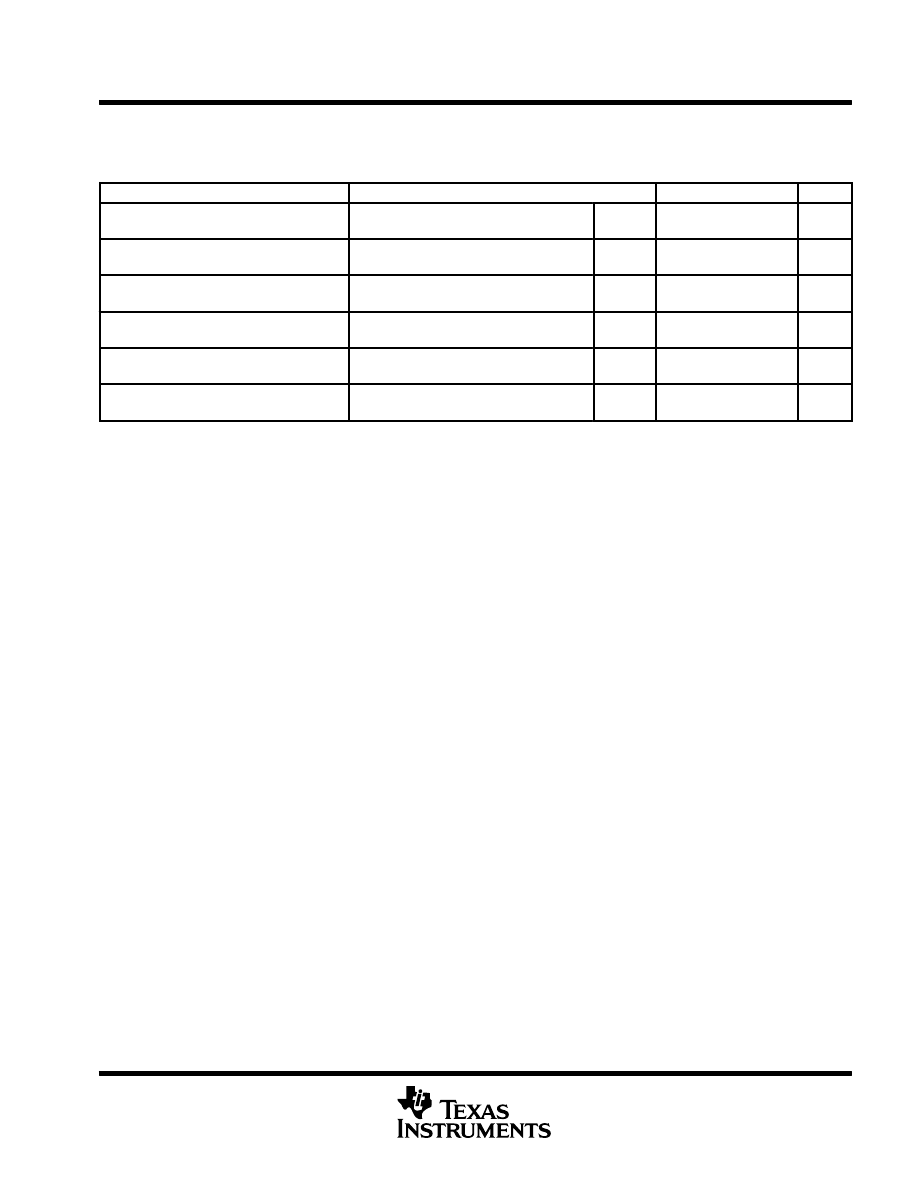
MSP430x13x, MSP430x14x
MIXED SIGNAL MICROCONTROLLER
SLAS272C – JULY 2000 – REVISED FEBRUARY 2001
49
POST OFFICE BOX 655303
•
DALLAS, TEXAS 75265
electrical characteristics over recommended operating free-air temperature (unless otherwise
noted) (continued)
12-bit ADC, built-in reference (see Note 41)
PARAMETER
TEST CONDITIONS
MIN
NOM
MAX
UNIT
IVeREF+
Static input current (see
Note 42)
0V
≤
VeREF+
≤
VAVCC
2.2 V/3 V
±
1
µ
A
IVREF–/VeREF–
Static input current (see
Note 42)
0V
≤
VeREF–
≤
VAVCC
2.2 V/3 V
±
1
µ
A
CVREF+
Capacitance at pin
VREF+ (see Note 43)
REFON =1,
0 mA
≤
IVREF+
≤
IV(REF)+(max)
2.2 V/3 V
5
10
µ
F
Ci ‡
Input capacitance (see
Note 44)
Only one terminal can be selected at one
time, P6.x/Ax
2.2 V
40
pF
Zi‡
Input MUX ON
resistance(see Note 44)
0V
≤
VAx
≤
VAVCC
3 V
2000
Ω
TREF+†
Temperature coefficient
of built-in reference
IV(REF)+ is a constant in the range of
0 mA
≤
IV(REF)+
≤
1 mA
2.2 V/3 V
±
100
ppm/
°
C
† Not production tested, limits characterized
‡ Not production tested, limits verified by design
NOTES: 41. The voltage source on VeREF+ and VREF–/VeREF–) needs to have low dynamic impedance for 12-bit accuracy to allow the charge
to settle for this accuracy (See Figures 12 and 13).
42. The external reference is used during conversion to charge and discharge the capacitance array. The dynamic impedance should
follow the recommendations on analog-source impedance to allow the charge to settle for 12-bit accuracy.
43. The internal buffer operational amplifier and the accuracy specifications require an external capacitor.
44. The input capacitance is also the dynamic load for an external reference during conversion. The dynamic impedance of the reference
supply should follow the recommendations on analog-source impedance to allow the charge to settle for 12-bit accuracy. All INL
and DNL tests uses two capacitors between pins V(REF+) and AVSS and V(REF–)/V(eREF–) and AVSS: 10
µ
F tantalum and 100 nF
ceramic.
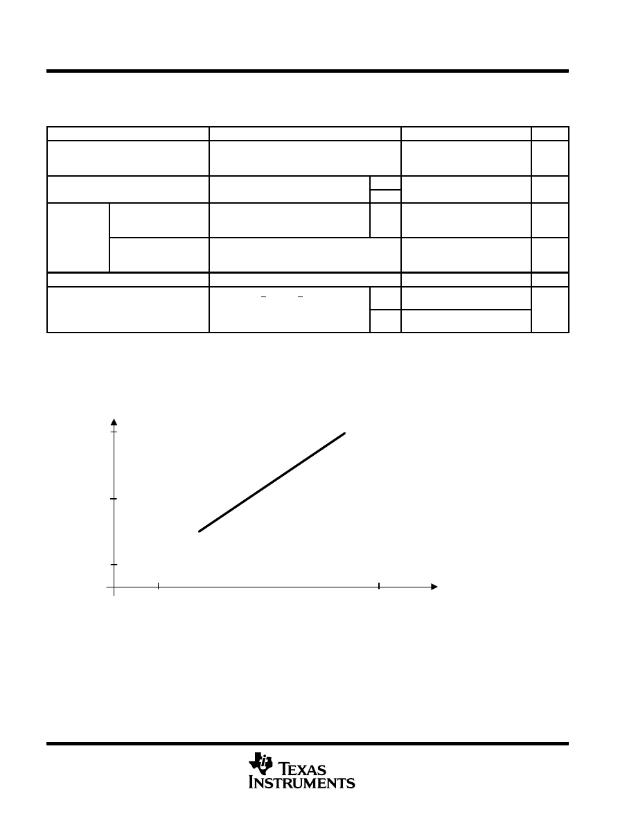
MSP430x13x, MSP430x14x
MIXED SIGNAL MICROCONTROLLER
SLAS272C – JULY 2000 – REVISED FEBRUARY 2001
50
POST OFFICE BOX 655303
•
DALLAS, TEXAS 75265
electrical characteristics over recommended operating free-air temperature (unless otherwise
noted) (continued)
12-bit ADC, timing parameters
PARAMETER
TEST CONDITIONS
MIN
NOM
MAX
UNIT
tREF(ON)†
Settle time of internal
reference voltage (see
Figure 15 and Note 45)
IV(REF)+ = 0.5 mA, CV(REF)+ = 10
µ
F,
VREF+ = 1.5 V, VAVCC = 2.2 V
17
ms
f(ADC12OSC)
ADC12DIV=0 [f(ADC12CLK)
2.2 V
3 7
6 3
MHz
f(ADC12OSC)
(
)
=f(ADC12OSC)]
3 V
3.7
6.3
MHz
tCONVERT
Conversion time
AVCC(min)
≤
VAVCC
≤
AVCC(max),
CVREF+
≥
5
µ
F, Internal oscillator,
fOSC = 3.7 MHz to 6.3 MHz
2.2 V/
3 V
2.06
3.51
µ
s
tCONVERT
Conversion time
AVCC(min)
≤
VAVCC
≤
AVCC(max),
External fADC12(CLK) from ACLK or MCLK or
SMCLK: ADC12SSEL
≠
0
13
×
ADC12DIV
×
1/fADC12(CLK)
µ
s
tADC12ON‡
Settle time of the ADC
AVCC(min)
≤
VAVCC
≤
AVCC(max) (see Note 46)
100
ns
tS
l
‡
Sampling time
VAVCC(min) < VAVCC < VAVCC(max)
Ri(source) = 400
Ω
, Zi = 1000
Ω
,
3 V
1220
ns
tSample‡
Sampling time
i(source)
i
Ci = 30 pF
τ
= [Ri(source) x+ Zi] x Ci;(see Note 47)
2.2 V
1400
ns
† Not production tested, limits characterized
‡ Not production tested, limits verified by design
NOTES: 45. The condition is that the error in a conversion started after tREF(ON) is less than
±
0.5 LSB. The settling time depends on the external
capacitive load.
46. The condition is that the error in a conversion started after tADC12ON is less than
±
0.5 LSB. The reference and input signal are already
settled.
47. Ten Tau (
τ
) are needed to get an error of less than
±
0.5 LSB. tSample = 10 x (Ri + Zi) x Ci+ 800 ns
CVREF+
1
µ
F
0
1 ms
10 ms
100 ms
tREF(ON)
t[REF(ON) ~ 0.66 x CVREF+ [ms] With C[VREF+] in
µ
F
100
µ
F
10
µ
F
Figure 15. Typical Settling Time of Internal Reference t
REF(ON)
vs External Capacitor on V
REF
+
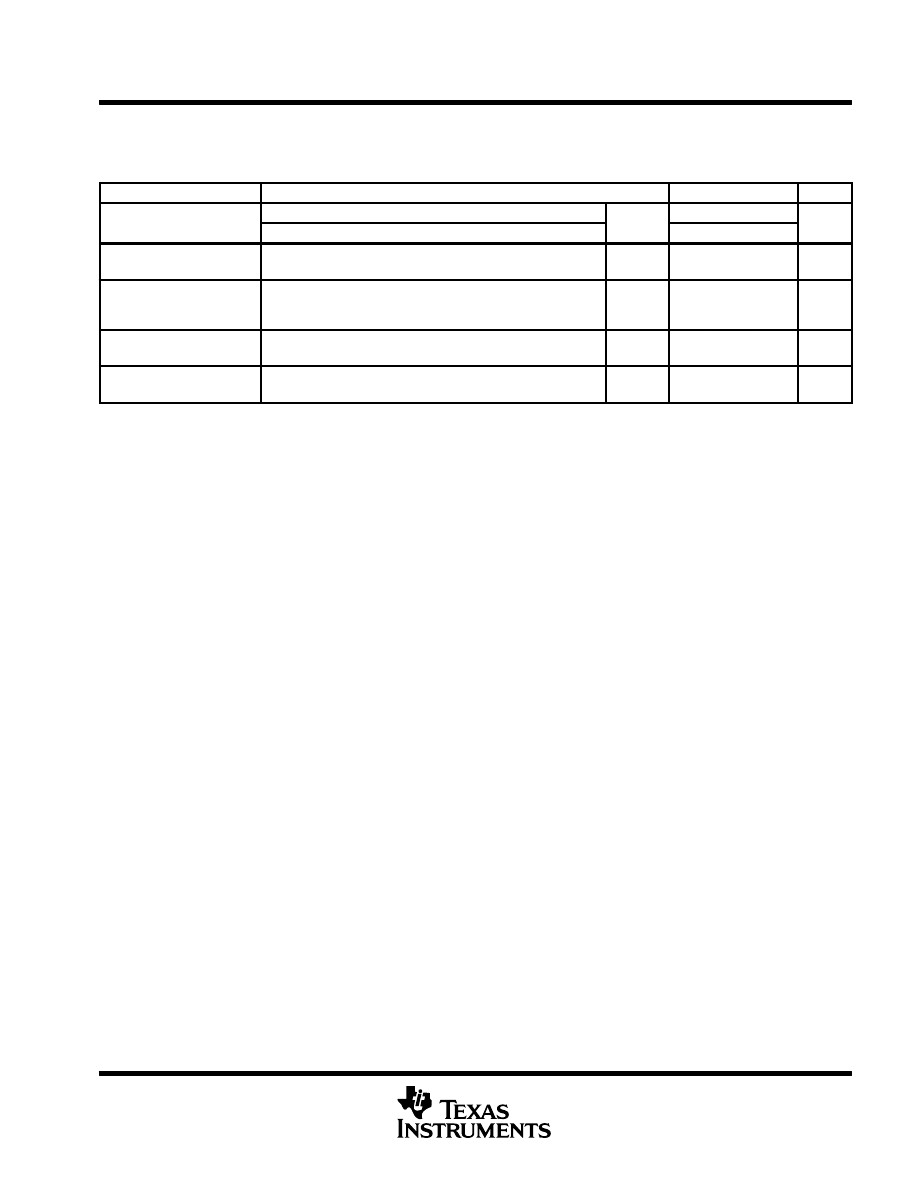
MSP430x13x, MSP430x14x
MIXED SIGNAL MICROCONTROLLER
SLAS272C – JULY 2000 – REVISED FEBRUARY 2001
51
POST OFFICE BOX 655303
•
DALLAS, TEXAS 75265
electrical characteristics over recommended operating free-air temperature (unless otherwise
noted) (continued)
12-bit ADC, linearity parameters
PARAMETER
TEST CONDITIONS
MIN
NOM
MAX
UNIT
E(I)
Integral linearity error
1.4 V
≤
(VeREF+ – VREF–/VeREF–) min
≤
1.6 V
2 2 V/3 V
±
2
LSB
E(I)
Integral linearity error
1.6 V < [V(eREF+) – V(REF–)/V(eREF–)] min
≤
[V(AVCC)]
2.2 V/3 V
±
1.7
LSB
ED
Differential linearity
error
(VeREF+ – VREF–/VeREF–)min
≤
(VeREF+ – VREF–/VeREF–),
C(VREF+) = 10
µ
F (tantalum) and 100 nF (ceramic)
2.2 V/3 V
±
1
LSB
EO
Offset error†
(VeREF+ – VREF–/VeREF–)min
≤
(VeREF+ – VREF–/VeREF–),
Internal impedance of source Ri < 100
Ω
,
C(VREF+) = 10
µ
F (tantalum) and 100 nF (ceramic)
2.2 V/3 V
±
2
±
4
LSB
EG
Gain error†
(VeREF+ – VREF–/VeREF–)min
≤
(VeREF+ – VREF–/VeREF–),
C(VREF+) = 10
µ
F (tantalum) and 100 nF (ceramic)
2.2 V/3 V
±
1.1
±
2
LSB
ET
Total unadjusted
error†
(VeREF+ – VREF–/VeREF–)min
≤
(VeREF+ – VREF–/VeREF–),
C(VREF+) = 10
µ
F (tantalum) and 100 nF (ceramic)
2.2 V/3 V
±
2
±
5
LSB
† Not production tested, limits characterized
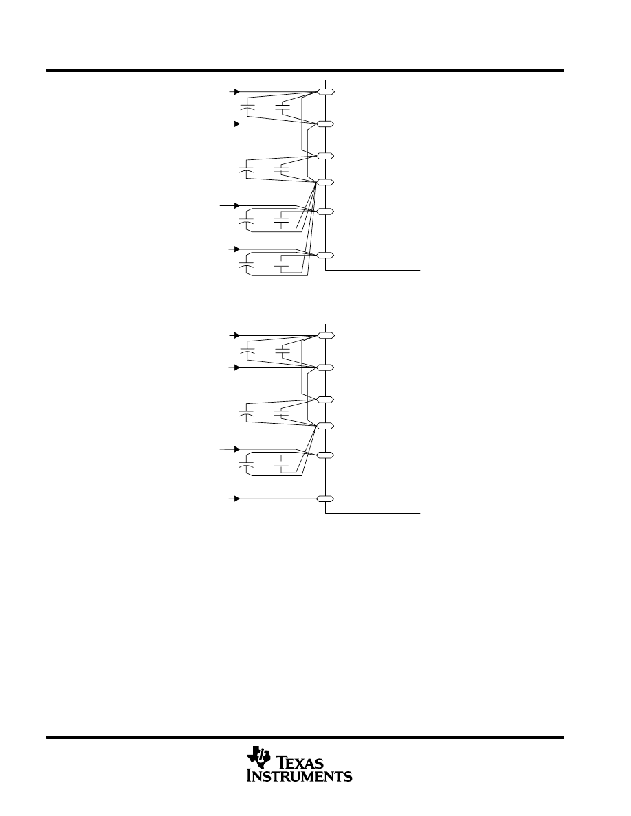
MSP430x13x, MSP430x14x
MIXED SIGNAL MICROCONTROLLER
SLAS272C – JULY 2000 – REVISED FEBRUARY 2001
52
POST OFFICE BOX 655303
•
DALLAS, TEXAS 75265
+
–
10
µ
F
100 nF
AVSS
MSP430F13x
MSP430F14x
+
–
+
–
10
µ
F
100 nF
10
µ
F
100 nF
AVCC
10
µ
F
100 nF
DVSS
DVCC
From
Power
Supply
Apply
External
Reference
+
–
Apply External Reference [V(eREF+)]
or Use Internal Reference [VREF+]
VREF+ or V(eREF+)
V(REF–)/V(eREF–)
Figure 16. Supply Voltage and Reference Voltage Design V
(REF–)/
V
(eREF–)
External Supply
+
–
10
µ
F
100 nF
AVSS
MSP430F13x
MSP430F14x
+
–
10
µ
F
100 nF
AVCC
10
µ
F
100 nF
DVSS
DVCC
From
Power
Supply
+
–
Apply External Reference [V(eREF+)]
or Use Internal Reference [VREF+]
VREF+ or V(eREF+)
V(REF–)/V(eREF–)
Reference Is Internally
Switched to AVSS
Figure 17. Supply Voltage and Reference Voltage Design V
(REF–)/
V
(eREF–)
=AV
SS
, Internally Connected
MSP430x13x, MSP430x14x
MIXED SIGNAL MICROCONTROLLER
SLAS272C – JULY 2000 – REVISED FEBRUARY 2001
53
POST OFFICE BOX 655303
•
DALLAS, TEXAS 75265
electrical characteristics over recommended operating free-air temperature (unless otherwise
noted) (continued)
12-bit ADC, temperature sensor and built-in Vmid
PARAMETER
TEST CONDITIONS
MIN
NOM
MAX
UNIT
ISENSOR
Operating supply current into
VREFON = 0, INCH = 0Ah,
2.2 V
40
120
µ
A
ISENSOR
g
y
AVCC terminal (see Note 48)
REFON
,
,
ADC12ON=NA, TA = 25
_
C
3 V
60
160
µ
A
VS
SO
†
ADC12ON = 1, INCH = 0Ah,
2.2 V
986
986
±
5%
mV
VSENSOR†
,
,
TA = 0
°
C
3 V
986
986
±
5%
mV
TCS
SO
†
ADC12ON = 1 INCH = 0Ah
2.2 V
3.55
3.55
±
3%
mV/
°
C
TCSENSOR†
ADC12ON = 1, INCH = 0Ah
3 V
3.55
3.55
±
3%
mV/
°
C
tS
SO (
)
†
Sample time required if channel
ADC12ON = 1, INCH = 0Ah,
2.2 V
30
µ
s
tSENSOR(sample)†
q
10 is selected (see Note 49)
,
,
Error of conversion result
≤
1 LSB
3 V
30
µ
s
IVMID
Current into divider at channel 11
ADC12ON = 1, INCH = 0Bh,
2.2 V
NA
µ
A
IVMID
Current into divider at channel 11
,
,
(see Note 50)
3 V
NA
µ
A
VMID
AVCC divider at channel 11
ADC12ON = 1, INCH = 0Bh,
2.2 V
1.1
1.1
±
0.04
V
VMID
AVCC divider at channel 11
,
,
VMID is ~0.5 x VAVCC
3 V
1.5
1.50
±
0.04
V
tON(VMID)
On-time if channel 11 is selected
ADC12ON = 1, INCH = 0Bh,
2.2 V
NA
ns
tON(VMID)
(see Note 51)
Error of conversion result
≤
1 LSB
3 V
NA
ns
† Not production tested, limits characterized
‡ Not production tested, limits verified by design
NOTES: 48. The sensor current ISENSOR is consumed if (ADC12ON = 1 and VREFON=1), or (ADC12ON=1 AND INCH=0Ah and sample signal
is high). Therefore it includes the constant current through the sensor and the reference.
49. The typical equivalent impedance of the sensor is 51 k
Ω
. The sample time needed is the sensor-on time tSENSOR(ON)
50. No additional current is needed. The VMID is used during sampling.
51. The on-time tON(VMID) is identical to sampling time tSample; no additional on time is needed.
JTAG, program memory and fuse
PARAMETER
TEST CONDITIONS
VCC
MIN
NOM
MAX
UNIT
f
JTAG/T
t
TCK frequency
2.2 V
DC
5
MHz
f(TCK)
JTAG/Test
(see Note 55)
TCK frequency
3 V
DC
10
MHz
(see Note 55)
Pullup resistors on TMS, TCK, TDI (see Note 52)
2.2 V/ 3V
25
60
90
k
Ω
VFB
JTAG/f
Fuse-blow voltage, F versions (see Note 54)
2.2 V/3 V
6.0
7.0
V
IFB
JTAG/fuse
(see Note 53)
Supply current on TDI with fuse blown
100
mA
IFB
(see Note 53)
Time to blow the fuse
1
ms
I(DD-PGM)
F-versions only
Current from DVCC when programming is active
2.7 V/3.6 V
3
5
mA
I(DD-Erase)
y
(see Note 55)
Current from DVCC when erase is active
2.7 V/3.6 V
3
5
mA
t( t ti )
F versions only
Write/erase cycles
104
105
cycles
t(retention)
F-versions only
Data retention TJ = 25
°
C
100
years
NOTES: 52. TMS, TDI, and TCK pull-up resistors are implemented in all F versions.
53. Once the fuse is blown, no further access to the MSP430 JTAG/test feature is possible. The JTAG block is switched to bypass mode.
54. The supply voltage to blow the fuse is applied to the TDI pin.
55. f(TCK) may be restricted to meet the timing requirements of the module selected. Duration of the program/erase cycle is determined
by f(FTG) applied to the flash timing controller. It can be calculated as follows:
t(word write) = 33 x 1/f(FTG)
t(segment write, byte 0) = 30 x
1/f(FTG)
t(segment write end sequence) =5 x 1/f(FTG)
t(mass erase) = 5296 x 1/f(FTG)
t(segment erase) = 4817 x 1/f(FTG)
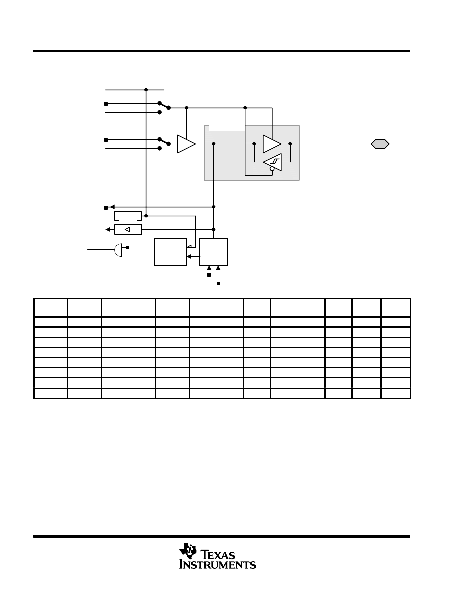
MSP430x13x, MSP430x14x
MIXED SIGNAL MICROCONTROLLER
SLAS272C – JULY 2000 – REVISED FEBRUARY 2001
54
POST OFFICE BOX 655303
•
DALLAS, TEXAS 75265
input/output schematic
port P1, P1.0 to P1.7, input/output with Schmitt-trigger
P1.0/TACLK ..
P1IN.x
Module X IN
Pad Logic
Interrupt
Flag
Edge
Select
Interrupt
P1SEL.x
P1IES.x
P1IFG.x
P1IE.x
P1IRQ.x
EN
D
Set
EN
Q
P1OUT.x
P1DIR.x
P1SEL.x
Module X OUT
Direction Control
From Module
0
1
0
1
P1.7/TA2
PnSel.x
PnDIR.x
Dir. CONTROL
FROM MODULE
PnOUT.x
MODULE X OUT
PnIN.x
MODULE X IN
PnIE.x
PnIFG.x
PnIES.x
P1Sel.0
P1DIR.0
P1DIR.0
P1OUT.0
DVSS
P1IN.0
TACLK†
P1IE.0
P1IFG.0
P1IES.0
P1Sel.1
P1DIR.1
P1DIR.1
P1OUT.1
Out0 signal†
P1IN.1
CCI0A†
P1IE.1
P1IFG.1
P1IES.1
P1Sel.2
P1DIR.2
P1DIR.2
P1OUT.2
Out1 signal†
P1IN.2
CCI1A†
P1IE.2
P1IFG.2
P1IES.2
P1Sel.3
P1DIR.3
P1DIR.3
P1OUT.3
Out2 signal†
P1IN.3
CCI2A†
P1IE.3
P1IFG.3
P1IES.3
P1Sel.4
P1DIR.4
P1DIR.4
P1OUT.4
SMCLK
P1IN.4
unused
P1IE.4
P1IFG.4
P1IES.4
P1Sel.5
P1DIR.5
P1DIR.5
P1OUT.5
Out0 signal†
P1IN.5
unused
P1IE.5
P1IFG.5
P1IES.5
P1Sel.6
P1DIR.6
P1DIR.6
P1OUT.6
Out1 signal†
P1IN.6
unused
P1IE.6
P1IFG.6
P1IES.6
P1Sel.7
P1DIR.7
P1DIR.7
P1OUT.7
Out2 signal†
P1IN.7
unused
P1IE.7
P1IFG.7
P1IES.7
† Signal from or to Timer_A
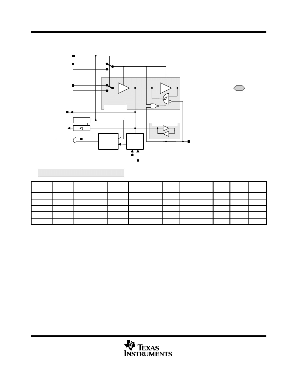
MSP430x13x, MSP430x14x
MIXED SIGNAL MICROCONTROLLER
SLAS272C – JULY 2000 – REVISED FEBRUARY 2001
55
POST OFFICE BOX 655303
•
DALLAS, TEXAS 75265
input/output schematic (continued)
port P2, P2.0 to P2.2, P2.6, and P2.7 input/output with Schmitt-trigger
P2IN.x
P2OUT.x
Pad Logic
P2DIR.x
P2SEL.x
Module X OUT
Edge
Select
Interrupt
P2SEL.x
P2IES.x
P2IFG.x
P2IE.x
P2IRQ.x
Direction Control
P2.0/ACLK
0
1
0
1
Interrupt
Flag
Set
EN
Q
Module X IN
EN
D
Bus Keeper
CAPD.X
P2.1/TAINCLK
P2.2/CAOUT/TA0
P2.6/ADC12CLK
P2.7/TA0
0: Input
1: Output
x: Bit Identifier 0 to 2, 6, and 7 for Port P2
From Module
PnSel.x
PnDIR.x
Dir. CONTROL
FROM MODULE
PnOUT.x
MODULE X OUT
PnIN.x
MODULE X IN
PnIE.x
PnIFG.x
PnIES.x
P2Sel.0
P2DIR.0
P2DIR.0
P2OUT.0
ACLK
P2IN.0
unused
P2IE.0
P2IFG.0
P2IES.0
P2Sel.1
P2DIR.1
P2DIR.1
P2OUT.1
DVSS
P2IN.1
INCLK‡
P2IE.1
P2IFG.1
P2IES.1
P2Sel.2
P2DIR.2
P2DIR.2
P2OUT.2
CAOUT†
P2IN.2
CCI0B‡
P2IE.2
P2IFG.2
P2IES.2
P2Sel.6
P2DIR.6
P2DIR.6
P2OUT.6
ADC12CLK¶
P2IN.6
unused
P2IE.6
P2IFG.6
P2IES.6
P2Sel.7
P2DIR.7
P2DIR.7
P2OUT.7
Out0 signal§
P2IN.7
unused
P2IE.7
P2IFG.7
P2IES.7
† Signal from Comparator_A
‡ Signal to Timer_A
§ Signal from Timer_A
¶ ADC12CLK signal is output of the 12-bit ADC module
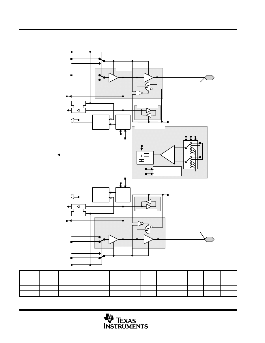
MSP430x13x, MSP430x14x
MIXED SIGNAL MICROCONTROLLER
SLAS272C – JULY 2000 – REVISED FEBRUARY 2001
56
POST OFFICE BOX 655303
•
DALLAS, TEXAS 75265
input/output schematic (continued)
port P2, P2.3 to P2.4, input/output with Schmitt-trigger
Bus Keeper
P2IN.3
P2OUT.3
Pad Logic
P2DIR.3
P2SEL.3
Module X OUT
Edge
Select
Interrupt
P2SEL.3
P2IES.3
P2IFG.3
P2IE.3
P2IRQ.3
Direction Control
From Module
P2.3/CA0/TA1
0
1
0
1
Interrupt
Flag
Set
EN
Q
Module X IN
EN
D
P2IN.4
P2OUT.4
Pad Logic
P2DIR.4
P2SEL.4
Module X OUT
Edge
Select
Interrupt
P2SEL.4
P2IES.4
P2IFG.4
P2IE.4
P2IRQ.4
Direction Control
From Module
P2.4/CA1/TA2
0
1
0
1
Interrupt
Flag
Set
EN
Q
Module X IN
EN
D
Comparator_A
–
+
Reference Block
CCI1B
CAF
CAREF
P2CA
CAEX
CAREF
Bus Keeper
CAPD.3
CAPD.4
To Timer_A3
0: Input
1: Output
0: Input
1: Output
PnSel.x
PnDIR.x
DIRECTION
CONTROL
FROM MODULE
PnOUT.x
MODULE X OUT
PnIN.x
MODULE X IN
PnIE.x
PnIFG.x
PnIES.x
P2Sel.3
P2DIR.3
P2DIR.3
P2OUT.3
Out1 signal†
P2IN.3
unused
P2IE.3
P2IFG.3
P2IES.3
P2Sel.4
P2DIR.4
P2DIR.4
P2OUT.4
Out2 signal†
P2IN.4
unused
P2IE.4
P2IFG.4
P2IES.4
† Signal from Timer_A
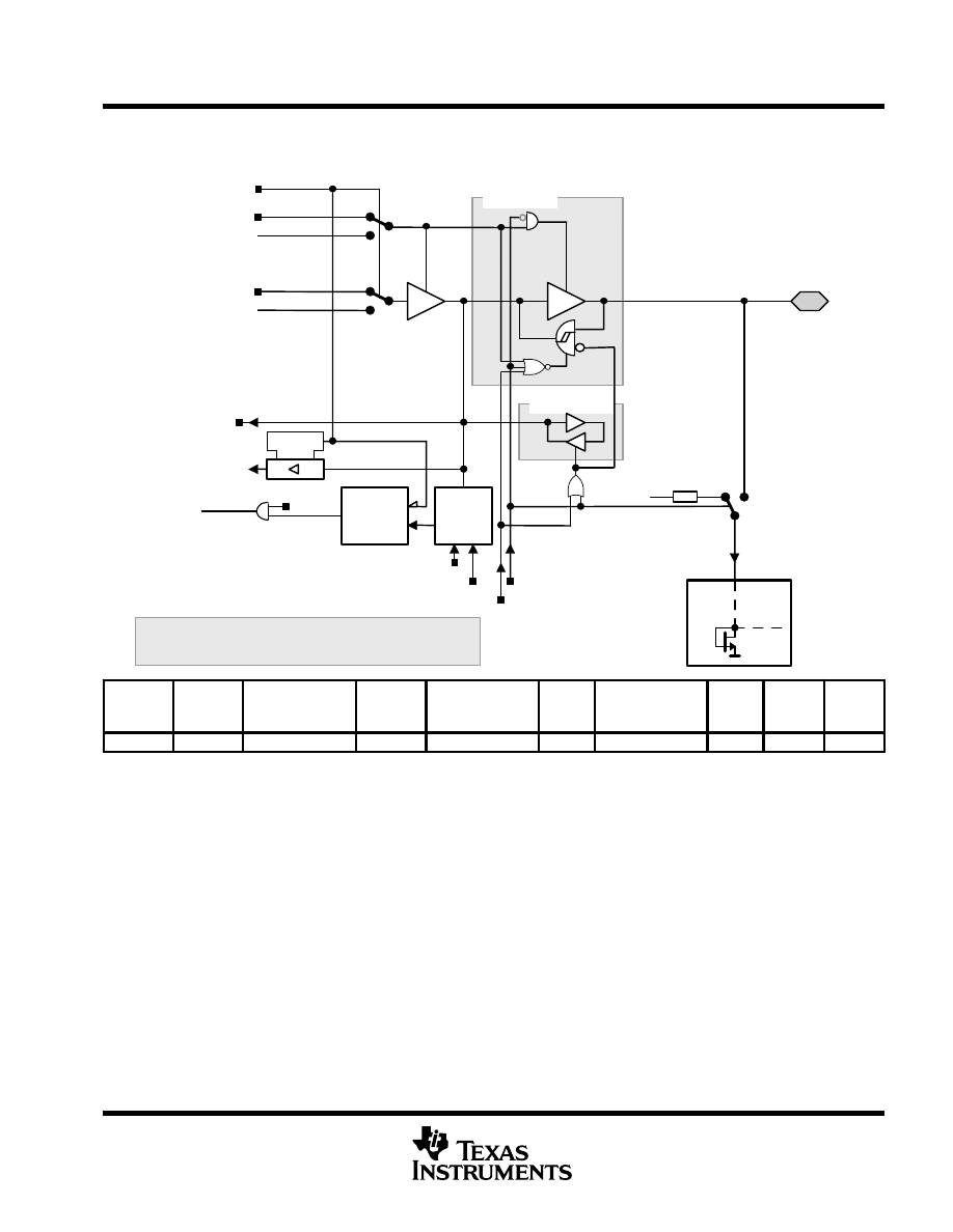
MSP430x13x, MSP430x14x
MIXED SIGNAL MICROCONTROLLER
SLAS272C – JULY 2000 – REVISED FEBRUARY 2001
57
POST OFFICE BOX 655303
•
DALLAS, TEXAS 75265
input/output schematic (continued)
port P2, P2.5, input/output with Schmitt-trigger and R
osc
function for the basic clock module
P2IN.5
P2OUT.5
Pad Logic
P2DIR.5
P2SEL.5
Module X OUT
Edge
Select
Interrupt
P2SEL.5
P2IES.5
P2IFG.5
P2IE.5
P2IRQ.5
Direction Control
P2.5/Rosc
0
1
0
1
Interrupt
Flag
Set
EN
Q
DCOR
Module X IN
EN
D
to
0
1
DC Generator
Bus Keeper
CAPD.5
DCOR: Control Bit From Basic Clock Module
If it Is Set, P2.5 Is Disconnected From P2.5 Pad
Internal to
Basic Clock
Module
VCC
0: Input
1: Output
From Module
PnSel.x
PnDIR.x
DIRECTION
CONTROL
FROM MODULE
PnOUT.x
MODULE X OUT
PnIN.x
MODULE X IN
PnIE.x
PnIFG.x
PnIES.x
P2Sel.5
P2DIR.5
P2DIR.5
P2OUT.5
DVSS
P2IN.5
unused
P2IE.5
P2IFG.5
P2IES.5
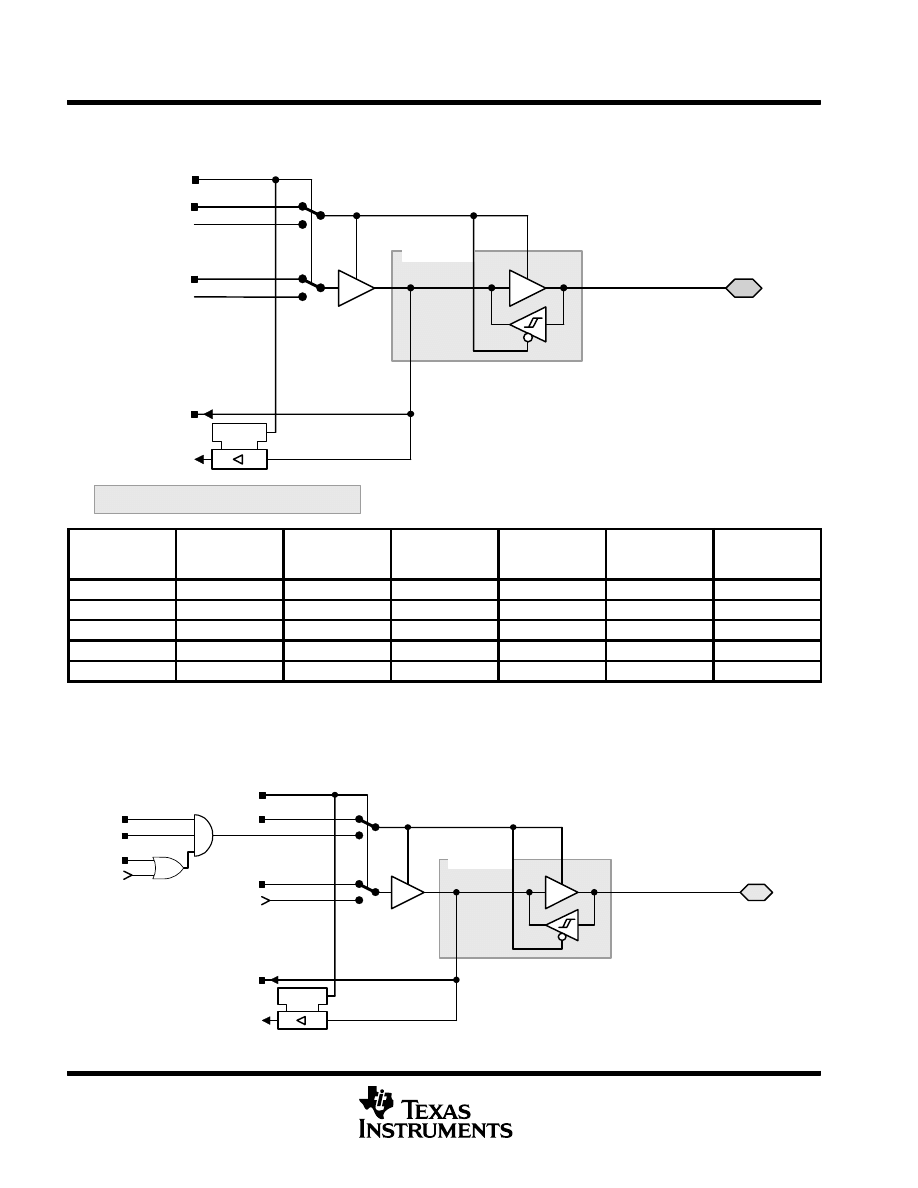
MSP430x13x, MSP430x14x
MIXED SIGNAL MICROCONTROLLER
SLAS272C – JULY 2000 – REVISED FEBRUARY 2001
58
POST OFFICE BOX 655303
•
DALLAS, TEXAS 75265
input/output schematic (continued)
port P3, P3.0 and P3.4 to P3.7, input/output with Schmitt-trigger
P3.0/STE0
P3IN.x
Module X IN
Pad Logic
EN
D
P3OUT.x
P3DIR.x
P3SEL.x
Module X OUT
Direction Control
From Module
0
1
0
1
P3.4/UTXD0
P3.5/URXD0
0: Input
1: Output
x: Bit Identifier, 0 and 4 to 7 for Port P3
P3.6/UTXD1‡
P3.7/URXD1¶
PnSel.x
PnDIR.x
DIRECTION
CONTROL
FROM MODULE
PnOUT.x
MODULE X OUT
PnIN.x
MODULE X IN
P3Sel.0
P3DIR.0
DVSS
P3OUT.0
DVSS
P3IN.0
STE0
P3Sel.4
P3DIR.4
DVCC
P3OUT.4
UTXD0†
P3IN.4
Unused
P3Sel.5
P3DIR.5
DVSS
P3OUT.5
DVSS
P3IN.5
URXD0§
P3Sel.6
P3DIR.6
DVCC
P3OUT.6
UTXD1‡
P3IN.6
Unused
P3Sel.7
P3DIR.7
DVSS
P3OUT.7
DVSS
P3IN.7
URXD1
¶
† Output from USART0 module
‡ Output from USART1 module in x14x configuration, DVSS in x13x configuration
§ Input to USART0 module
¶ Input to USART1 module in x14x configuration, unused in x13x configuration
port P3, P3.1, input/output with Schmitt-trigger
P3.1/SIMO0
P3IN.1
Pad Logic
EN
D
P3OUT1
P3DIR.1
P3SEL.1
(SI)MO0
0
1
0
1
DCM_SIMO
SYNC
MM
STE
STC
From USART0
SI(MO)0
To USART0
0: Input
1: Output
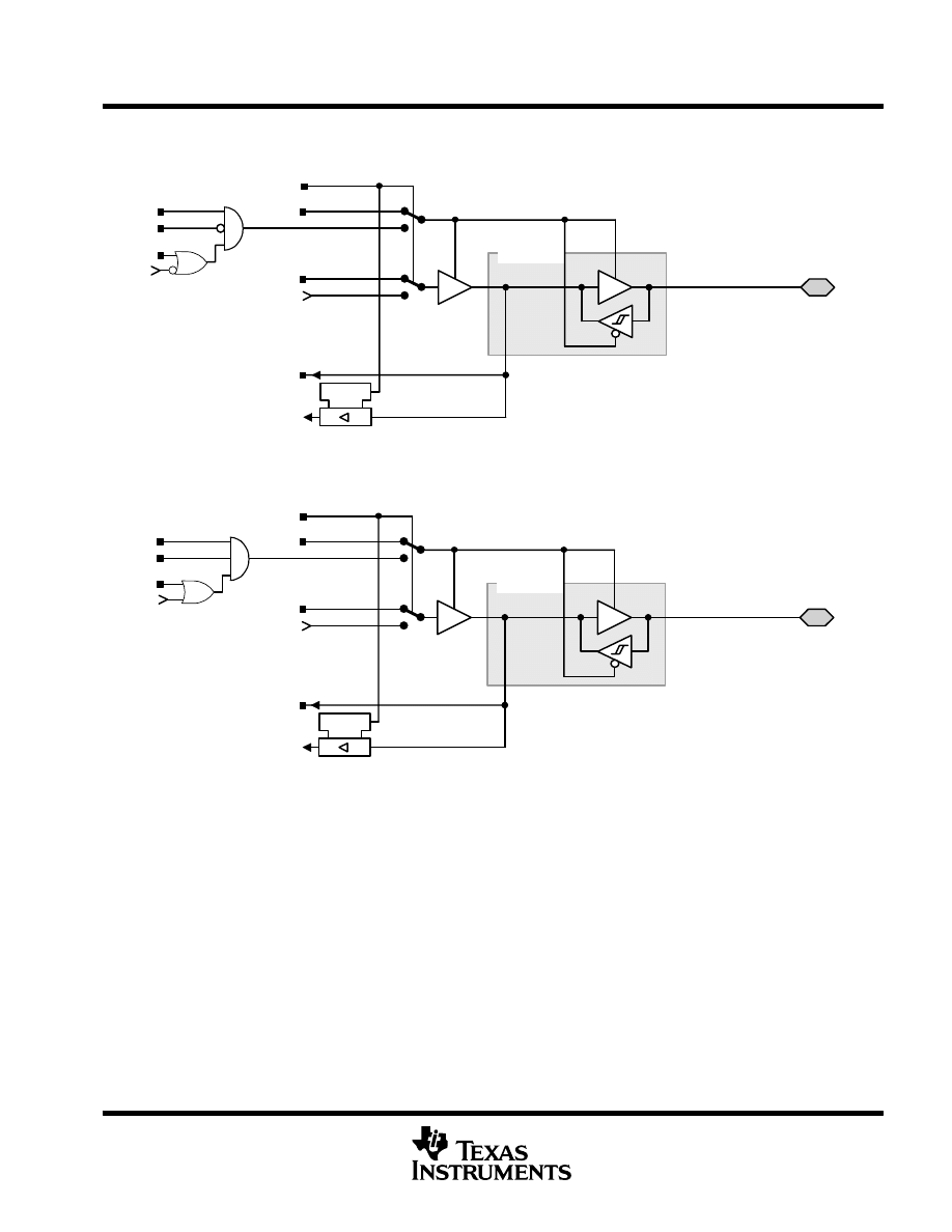
MSP430x13x, MSP430x14x
MIXED SIGNAL MICROCONTROLLER
SLAS272C – JULY 2000 – REVISED FEBRUARY 2001
59
POST OFFICE BOX 655303
•
DALLAS, TEXAS 75265
input/output schematic (continued)
port P3, P3.2, input/output with Schmitt-trigger
P3.2/SOMI0
P3IN.2
Pad Logic
EN
D
P3OUT.2
P3DIR.2
P3SEL.2
0
1
0
1
DCM_SOMI
SYNC
MM
STE
STC
SO(MI)0
From USART0
(SO)MI0
To USART0
0: Input
1: Output
port P3, P3.3, input/output with Schmitt-trigger
P3.3/UCLK0
P3IN.3
Pad Logic
EN
D
P3OUT.3
P3DIR.3
P3SEL.3
UCLK.0
0
1
0
1
DCM_UCLK
SYNC
MM
STE
STC
From USART0
UCLK0
To USART0
0: Input
1: Output
NOTE: UART mode:
The UART clock can only be an input. If UART mode and UART function are selected, the P3.3/UCLK0 is always
an input.
SPI, slave mode:
The clock applied to UCLK0 is used to shift data in and out.
SPI, master mode:
The clock to shift data in and out is supplied to connected devices on pin P3.3/UCLK0 (in slave mode).
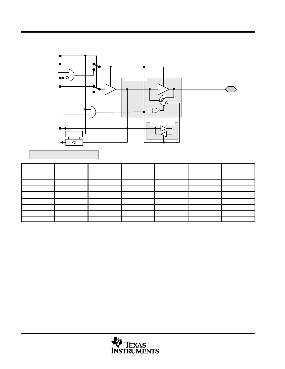
MSP430x13x, MSP430x14x
MIXED SIGNAL MICROCONTROLLER
SLAS272C – JULY 2000 – REVISED FEBRUARY 2001
60
POST OFFICE BOX 655303
•
DALLAS, TEXAS 75265
input/output schematic (continued)
port P4, P4.0 to P4.6, input/output with Schmitt-trigger
P4.0/TB0 ..
P4IN.x
Module X IN
Pad Logic
EN
D
x: bit identifier, 0 to 6 for Port P4
P4OUT.x
P4DIR.x
P4SEL.x
Module X OUT
Direction Control
From Module
0
1
0
1
Bus Keeper
TBoutHiZ
P4.6/TB6
0: Input
1: Output
PnSel.x
PnDIR.x
DIRECTION
CONTROL
FROM MODULE
PnOUT.x
MODULE X OUT
PnIN.x
MODULE X IN
P4Sel.0
P4DIR.0
P4DIR.0
P4OUT.0
Out0 signal†
P4IN.0
CCI0A / CCI0B‡
P4Sel.1
P4DIR.1
P4DIR.1
P4OUT.1
Out1 signal†
P4IN.1
CCI1A / CCI1B‡
P4Sel.2
P4DIR.2
P4DIR.2
P4OUT.2
Out2 signal†
P4IN.2
CCI2A / CCI2B‡
P4Sel.3
P4DIR.3
P4DIR.3
P4OUT.3
Out3 signal†
P4IN.3
CCI3A / CCI3B‡
P4Sel.4
P4DIR.4
P4DIR.4
P4OUT.4
Out4 signal†
P4IN.4
CCI4A / CCI4B‡
P4Sel.5
P4DIR.5
P4DIR.5
P4OUT.5
Out5 signal†
P4IN.5
CCI5A / CCI5B‡
P4Sel.6
P4DIR.6
P4DIR.6
P4OUT.6
Out6 signal†
P4IN.6
CCI6A / CCI6B‡
† Signal from Timer_B
‡ Signal to Timer_B
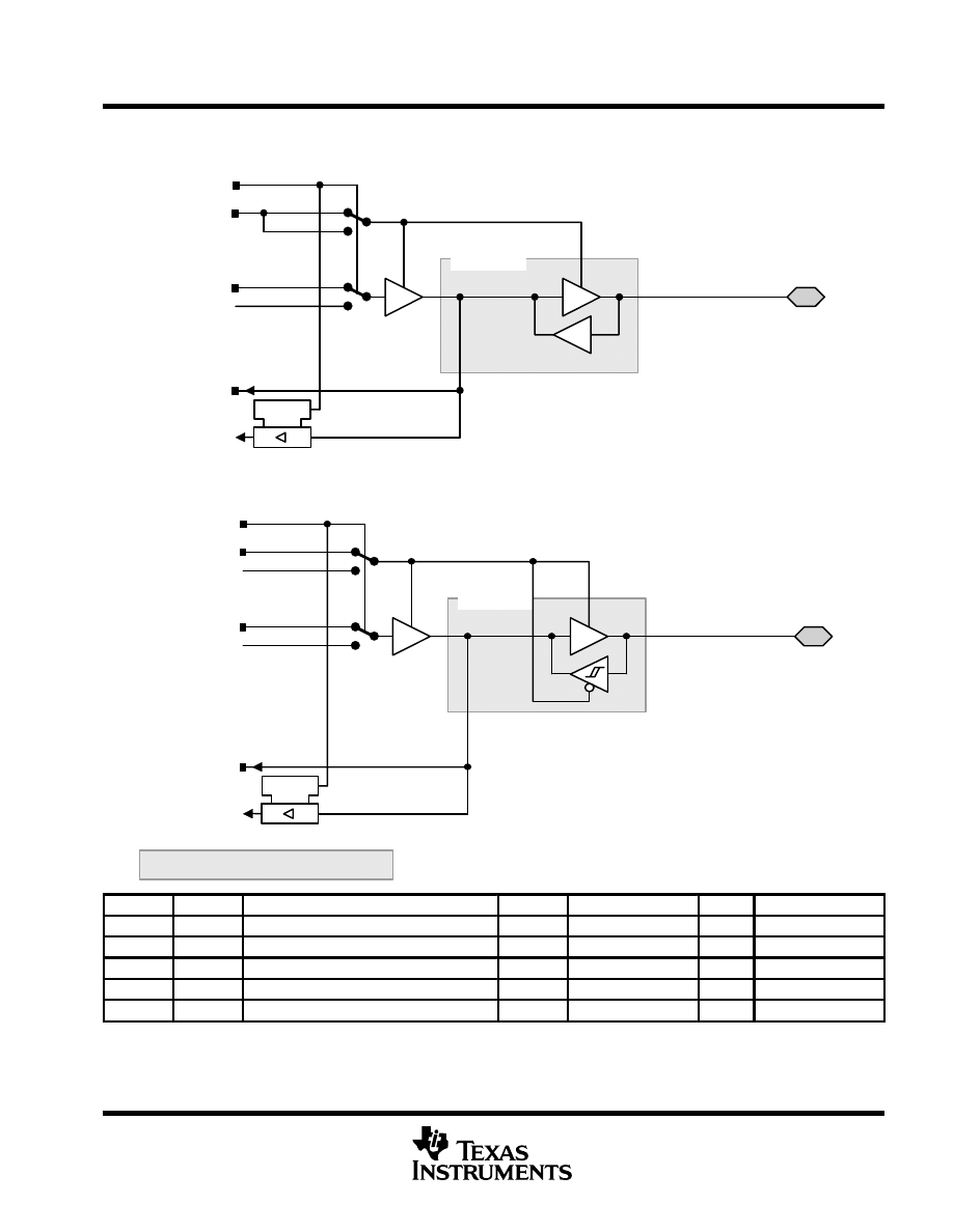
MSP430x13x, MSP430x14x
MIXED SIGNAL MICROCONTROLLER
SLAS272C – JULY 2000 – REVISED FEBRUARY 2001
61
POST OFFICE BOX 655303
•
DALLAS, TEXAS 75265
input/output schematic (continued)
port P4, P4.7, input/output with Schmitt-trigger
P4.7/TBCLK
P4IN.7
Timer_B,
Pad Logic
EN
D
P4OUT.7
P4DIR.7
P4SEL.7
0
1
0
1
TBCLK
0: Input
1: Output
DVSS
port P5, P5.0 and P5.4 to P5.7, input/output with Schmitt-trigger
P5.0/STE1
P5IN.x
Module X IN
Pad Logic
EN
D
P5OUT.x
P5DIR.x
P5SEL.x
Module X OUT
Direction Control
From Module
0
1
0
1
P5.4/MCLK
P5.5/SMCLK
P5.6/ACLK
P5.7/TBOutH
x: Bit Identifier, 0 and 4 to 7 for Port P5
0: Input
1: Output
PnSel.x
PnDIR.x
Dir. CONTROL FROM MODULE
PnOUT.x
MODULE X OUT
PnIN.x
MODULE X IN
P5Sel.0
P5DIR.0
DVSS
P5OUT.0
DVSS
P5IN.0
STE.1
P5Sel.4
P5DIR.4
DVCC
P5OUT.4
MCLK
P5IN.4
unused
P5Sel.5
P5DIR.5
DVCC
P5OUT.5
SMCLK
P5IN.5
unused
P5Sel.6
P5DIR.6
DVCC
P5OUT.6
ACLK
P5IN.6
unused
P5Sel.7
P5DIR.7
DVSS
P5OUT.7
DVSS
P5IN.7
TBoutHiZ
NOTE: TBoutHiZ signal is used by port module P4, pins P4.0 to P4.6. The function of TboutHiZ is mainly useful when used with Timer_B7.
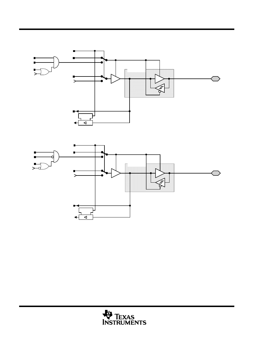
MSP430x13x, MSP430x14x
MIXED SIGNAL MICROCONTROLLER
SLAS272C – JULY 2000 – REVISED FEBRUARY 2001
62
POST OFFICE BOX 655303
•
DALLAS, TEXAS 75265
input/output schematic (continued)
port P5, P5.1, input/output with Schmitt-trigger
P5.1/SIMO1
P5IN.1
Pad Logic
EN
D
P5OUT.1
P5DIR.1
P5SEL.1
0
1
0
1
DCM_SIMO
SYNC
MM
STE
STC
(SI)MO1
From USART1
SI(MO)1
To USART1
0: Input
1: Output
port P5, P5.2, input/output with Schmitt-trigger
P5.2/SOMI1
P5IN.2
Pad Logic
EN
D
P5OUT.2
P5DIR.2
P5SEL.2
0
1
0
1
DCM_SOMI
SYNC
MM
STE
STC
SO(MI)1
From USART1
(SO)MI1
To USART1
0: Input
1: Output
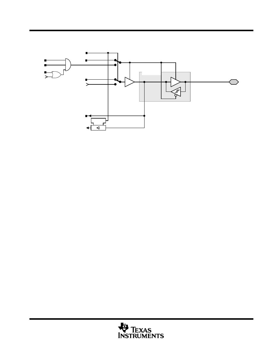
MSP430x13x, MSP430x14x
MIXED SIGNAL MICROCONTROLLER
SLAS272C – JULY 2000 – REVISED FEBRUARY 2001
63
POST OFFICE BOX 655303
•
DALLAS, TEXAS 75265
input/output schematic (continued)
port P5, P5.3, input/output with Schmitt-trigger
P5.3/UCLK1
P5IN.3
Pad Logic
EN
D
P5OUT.3
P5DIR.3
P5SEL.3
0
1
0
1
DCM_SIMO
SYNC
MM
STE
STC
UCLK1
From USART1
UCLK1
To USART1
0: Input
1: Output
NOTE: UART mode:
The UART clock can only be an input. If UART mode and UART function are selected, the P5.3/UCLK1 direction
is always input.
SPI, slave mode:
The clock applied to UCLK1 is used to shift data in and out.
SPI, master mode:
The clock to shift data in and out is supplied to connected devices on pin P5.3/UCLK1 (in slave mode).
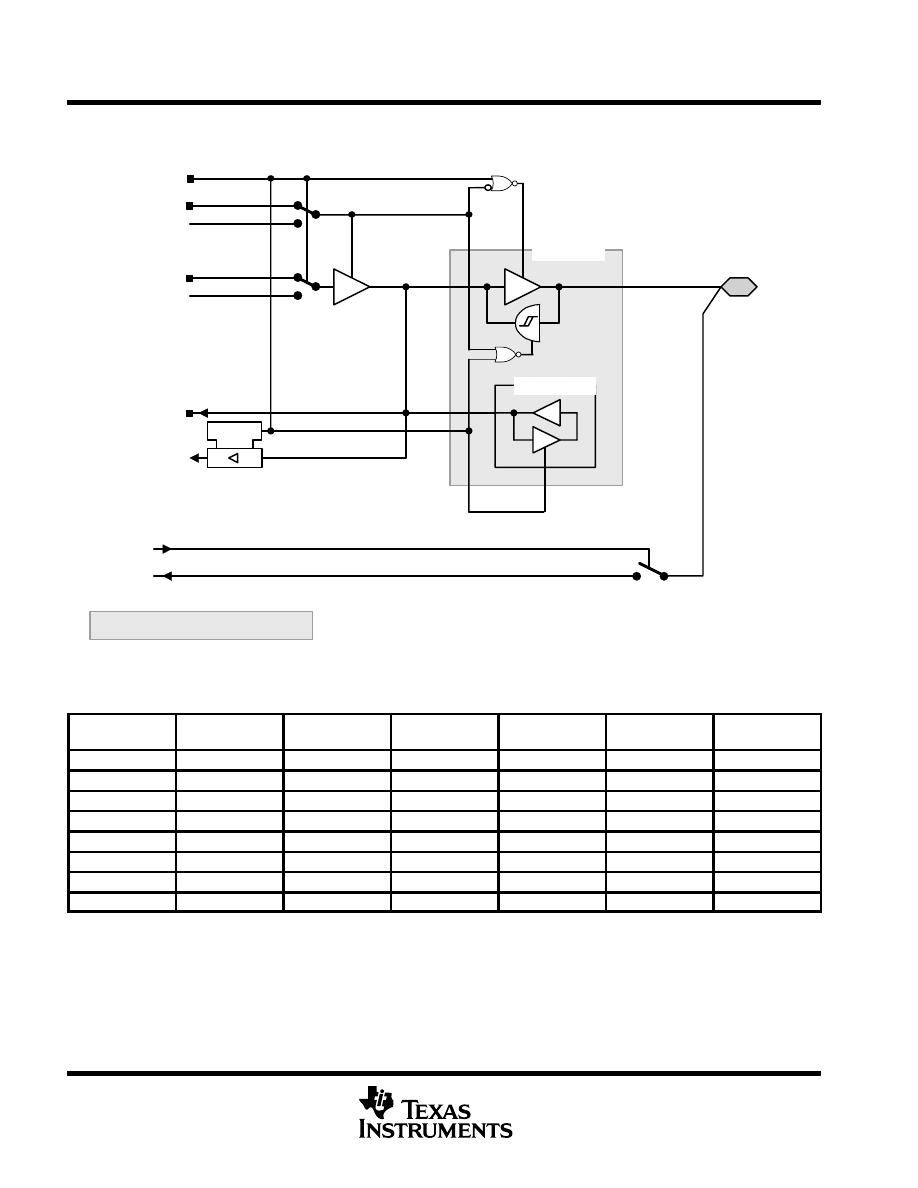
MSP430x13x, MSP430x14x
MIXED SIGNAL MICROCONTROLLER
SLAS272C – JULY 2000 – REVISED FEBRUARY 2001
64
POST OFFICE BOX 655303
•
DALLAS, TEXAS 75265
input/output schematic (continued)
port P6, P6.0 to P6.7, input/output with Schmitt-trigger
P6.0 .. P6.7
P6IN.x
Module X IN
Pad Logic
EN
D
P6OUT.x
P6DIR.x
P6SEL.x
Module X OUT
Direction Control
From Module
0
1
0
1
Bus Keeper
To ADC
From ADC
0: Input
1: Output
x: Bit Identifier, 0 to 7 for Port P6
NOTE: Analog signals applied to digital gates can cause current flow from the positive to the negative terminal. The throughput current flows if
the analog signal is in the range of transitions 0
→
1 or 1
←
0. The value of the throughput current depends on the driving capability of the
gate. For MSP430, it is approximately 100
µ
A.
Use P6SEL.x=1 to prevent throughput current. P6SEL.x should be set, even if the signal at the pin is not being used by the ADC12.
PnSel.x
PnDIR.x
DIR. CONTROL
FROM MODULE
PnOUT.x
MODULE X OUT
PnIN.x
MODULE X IN
P6Sel.0
P6DIR.0
P6DIR.0
P6OUT.0
DVSS
P6IN.0
unused
P6Sel.1
P6DIR.1
P6DIR.1
P6OUT.1
DVSS
P6IN.1
unused
P6Sel.2
P6DIR.2
P6DIR.2
P6OUT.2
DVSS
P6IN.2
unused
P6Sel.3
P6DIR.3
P6DIR.3
P6OUT.3
DVSS
P6IN.3
unused
P6Sel.4
P6DIR.4
P6DIR.4
P6OUT.4
DVSS
P6IN.4
unused
P6Sel.5
P6DIR.5
P6DIR.5
P6OUT.5
DVSS
P6IN.5
unused
P6Sel.6
P6DIR.6
P6DIR.6
P6OUT.6
DVSS
P6IN.6
unused
P6Sel.7
P6DIR.7
P6DIR.7
P6OUT.7
DVSS
P6IN.7
unused
NOTE: The signal at pins P6.x/Ax is used by the 12-bit ADC module.
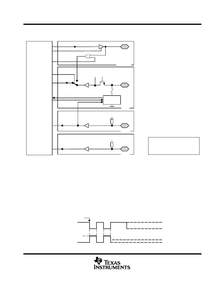
MSP430x13x, MSP430x14x
MIXED SIGNAL MICROCONTROLLER
SLAS272C – JULY 2000 – REVISED FEBRUARY 2001
65
POST OFFICE BOX 655303
•
DALLAS, TEXAS 75265
input/output schematic (continued)
JTAG pins TMS, TCK, TDI, TDO/TDI, input/output with Schmitt-trigger
TDI
TDO
TMS
TCK
Test
JTAG
see Note 1
&
Emulation
Module
Burn & Test
Fuse
Controlled by JTAG
Controlled by JTAG
Controlled
by JTAG
DVCC
DVCC
DVCC
During Programming Activity and
During Blowing of the Fuse, Pin
TDO/TDI Is Used to Apply the Test
Input Data for JTAG Circuitry
TDO/TDI
TDI
TMS
TCK
Fuse
DVCC
JTAG fuse check mode
MSP430 devices that have the fuse on the TDI terminal have a fuse check mode that tests the continuity of the
fuse the first time the JTAG port is accessed after a power-on reset (POR). When activated, a fuse check current,
I
TF
, of 1 mA at 3 V, 2.5 mA at 5 V can flow from the TDI pin to ground if the fuse is not burned. Care must be
taken to avoid accidentally activating the fuse check mode and increasing overall system power consumption.
Activation of the fuse check mode occurs with the first negative edge on the TMS pin after power up or if the
TMS is being held low during power up. The second positive edge on the TMS pin deactivates the fuse check
mode. After deactivation, the fuse check mode remains inactive until another POR occurs. After each POR the
fuse check mode has the potential to be activated.
The fuse check current will only flow when the fuse check mode is active and the TMS pin is in a low state (see
Figure 18). Therefore, the additional current flow can be prevented by holding the TMS pin high (default
condition).
Time TMS Goes Low After POR
TMS
ITF
ITDI
Figure 18. Fuse Check Mode Current, MSP430F13x, MSP430F14x
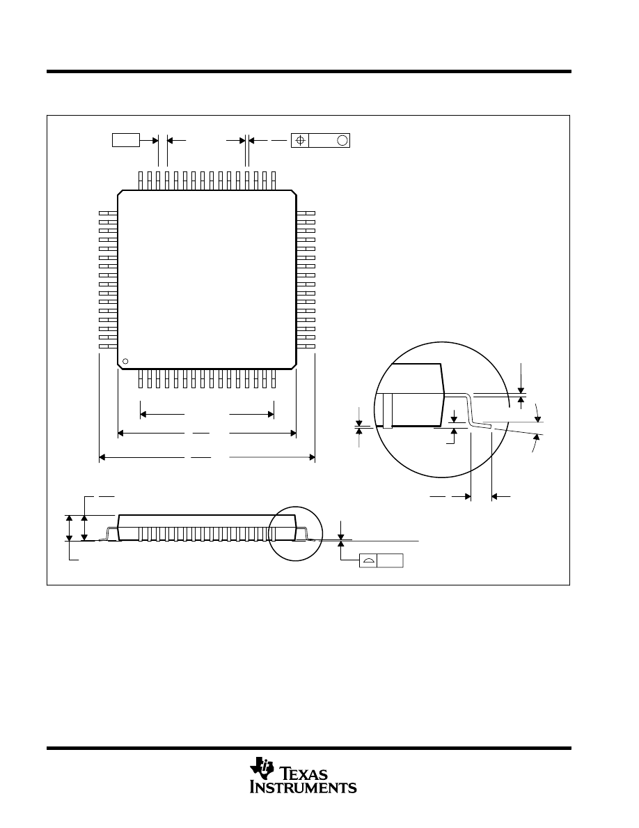
MSP430x13x, MSP430x14x
MIXED SIGNAL MICROCONTROLLER
SLAS272C – JULY 2000 – REVISED FEBRUARY 2001
66
POST OFFICE BOX 655303
•
DALLAS, TEXAS 75265
MECHANICAL DATA
PM (S-PQFP-G64)
PLASTIC QUAD FLATPACK
4040152 / C 11/96
32
17
0,13 NOM
0,25
0,45
0,75
Seating Plane
0,05 MIN
Gage Plane
0,27
33
16
48
1
0,17
49
64
SQ
SQ
10,20
11,80
12,20
9,80
7,50 TYP
1,60 MAX
1,45
1,35
0,08
0,50
M
0,08
0
°
– 7
°
NOTES: A. All linear dimensions are in millimeters.
B. This drawing is subject to change without notice.
C. Falls within JEDEC MS-026
D. May also be thermally enhanced plastic with leads connected to the die pads.

IMPORTANT NOTICE
Texas Instruments and its subsidiaries (TI) reserve the right to make changes to their products or to discontinue
any product or service without notice, and advise customers to obtain the latest version of relevant information
to verify, before placing orders, that information being relied on is current and complete. All products are sold
subject to the terms and conditions of sale supplied at the time of order acknowledgment, including those
pertaining to warranty, patent infringement, and limitation of liability.
TI warrants performance of its products to the specifications applicable at the time of sale in accordance with
TI’s standard warranty. Testing and other quality control techniques are utilized to the extent TI deems necessary
to support this warranty. Specific testing of all parameters of each device is not necessarily performed, except
those mandated by government requirements.
Customers are responsible for their applications using TI components.
In order to minimize risks associated with the customer’s applications, adequate design and operating
safeguards must be provided by the customer to minimize inherent or procedural hazards.
TI assumes no liability for applications assistance or customer product design. TI does not warrant or represent
that any license, either express or implied, is granted under any patent right, copyright, mask work right, or other
intellectual property right of TI covering or relating to any combination, machine, or process in which such
products or services might be or are used. TI’s publication of information regarding any third party’s products
or services does not constitute TI’s approval, license, warranty or endorsement thereof.
Reproduction of information in TI data books or data sheets is permissible only if reproduction is without
alteration and is accompanied by all associated warranties, conditions, limitations and notices. Representation
or reproduction of this information with alteration voids all warranties provided for an associated TI product or
service, is an unfair and deceptive business practice, and TI is not responsible nor liable for any such use.
Resale of TI’s products or services with
statements different from or beyond the parameters stated by TI for
that product or service voids all express and any implied warranties for the associated TI product or service,
is an unfair and deceptive business practice, and TI is not responsible nor liable for any such use.
Also see: Standard Terms and Conditions of Sale for Semiconductor Products. www.ti.com/sc/docs/stdterms.htm
Mailing Address:
Texas Instruments
Post Office Box 655303
Dallas, Texas 75265
Copyright
2001, Texas Instruments Incorporated
Wyszukiwarka
Podobne podstrony:
3 LCD LCD MSP430 id 755238 Nieznany (2)
msp430f1122
msp430g2553
MSP430 2005www
MSP430 wprzykładach cz2
msp430f123
MSP430X
MSP430 wprzykładach cz3
msp430f149 (2)
msp430fg4618
msp430 opis p ytki
MSP430 wprzykładach cz1
MSP430 wprzykładach cz8
msp430f110
msp430f1101a
msp430f149
MSP430 wprzykładach cz6
więcej podobnych podstron