MSP430F11x
MIXED SIGNAL MICROCONTROLLER
SLAS256B – NOVEMBER 1999 – REVISED JUNE 2000
1
POST OFFICE BOX 655303
•
DALLAS, TEXAS 75265
D
Low Supply Voltage Range 1.8 V – 3.6 V
D
Ultralow-Power Consumption
Low Operation Current,
1.6
µ
A at 4 kHz, 2.2 V
200
µ
A at 1 MHz, 2.2 V
D
Five Power Saving Modes:
(Standby Mode: 0.8
µ
A,
RAM Retention Off Mode: 0.1
µ
A)
D
Wake-Up From Standby Mode in 6
µ
s
D
16-Bit RISC Architecture, 125 ns
Instruction Cycle Time
D
Basic Clock Module Configurations:
– Various Internal Resistors
– Single External Resistor
– 32 kHz Crystal
– High Frequency Crystal
– Resonator
– External Clock Source
D
16-Bit Timer With Three Capture/Compare
Registers
D
Slope A/D Converter With External
Components
D
Serial Onboard Programming
D
Family Members Include:
MSP430F110:
1KB + 128B Flash Memory
128B RAM
MSP430F112:
4KB + 256B Flash Memory
256B RAM
D
Available in a 20-Pin Plastic Small-Outline
Wide Body (SOWB) Package and 20-Pin
Plastic Thin Shrink Small-Outline Package
(TSSOP)
description
The Texas Instruments MSP430 series is an ultralow-power microcontroller family consisting of several devices
featuring different sets of modules targeted to various applications. The microcontroller is designed to be battery
operated for an extended application lifetime. With 16-bit RISC architecture, 16 bit integrated registers on the
CPU, and the constant generator, the MSP430 achieves maximum code efficiency. The digitally-controlled
oscillator provides fast wake-up from all low-power modes to active mode in less than 6
m
s.
Typical applications include sensor systems that capture analog signals, convert them to digital values, and then
process the data and display them or transmit them to a host system. Stand alone RF sensor front end is another
area of application. The I/O port inputs provide single slope A/D conversion capability on resistive sensors. The
MSP430x11x series is an ultralow-power mixed signal microcontroller with a built in 16-bit timer and fourteen
I/O pins. The MSP430x11x1 family adds a versatile analog comparator.
The flash memory provides added flexibility of in-system programming and data storage without significantly
increasing the current consumption of the device. The programming voltage is generated on-chip, thereby
alleviating the need for an additional supply, and even allowing for reprogramming of battery-operated systems.
Copyright
2000, Texas Instruments Incorporated
PRODUCTION DATA information is current as of publication date.
Products conform to specifications per the terms of Texas Instruments
standard warranty. Production processing does not necessarily include
testing of all parameters.
1
2
3
4
5
6
7
8
9
10
20
19
18
17
16
15
14
13
12
11
TEST
V
CC
P2.5/R
osc
V
SS
XOUT/TCLK
XIN
RST/NMI
P2.0/ACLK
P2.1/INCLK
P2.2/TA0
P1.7/TA2/TDO/TDI
P1.6/TA1/TDI
P1.5/TA0/TMS
P1.4/SMCLK/TCK
P1.3/TA2
P1.2/TA1
P1.1/TA0
P1.0/TACLK
P2.4/TA2
P2.3/TA1
DW OR PW PACKAGE
(TOP VIEW)
Please be aware that an important notice concerning availability, standard warranty, and use in critical applications of
Texas Instruments semiconductor products and disclaimers thereto appears at the end of this data sheet.
MSP430F11x
MIXED SIGNAL MICROCONTROLLER
SLAS256B – NOVEMBER 1999 – REVISED JUNE 2000
2
POST OFFICE BOX 655303
•
DALLAS, TEXAS 75265
AVAILABLE OPTIONS
PACKAGED DEVICES
TA
PLASTIC
20-PIN SOWB
(DW)
PLASTIC
20-PIN TSSOP
(PW)
– 40
°
C to 85
°
C
MSP430F110IDW
MSP430F112IDW
MSP430F110IPW
MSP430F112IPW
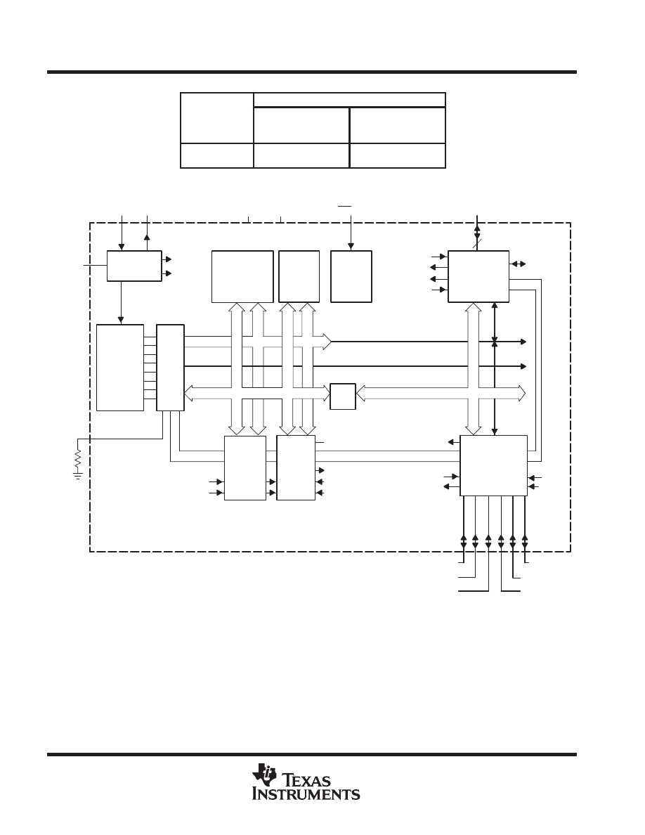
functional block diagram
Oscillator
System Clock
ACLK
SMCLK
1/4 KB Flash
128/256B
RAM
Power-on-
Reset
I/O Port P1
8 I/O’s, All With
Interrupt
CPU
Incl. 16 Reg.
Test
JTAG
Bus
Conv.
MAB, 16 Bit
MDB, 16 Bit
MAB, 4 Bit
MDB, 8 Bit
MCB
XIN
XOUT
VCC
VSS
RST/NMI
P1.0–7
DCOR
ACLK
P2.0 / ACLK
Rosc
TEST
Outx
Timer_A
3 CC
CCR0/1/2
Watchdog
Timer
15/16 Bit
MCLK
x = 0, 1, 2
ACLK
SMCLK
Outx
CCIxA
CCIxB
TACLK or
INCLK
INCLK
Out0
CCI1B
JTAG
CCIxA
TACLK
SMCLK
I/O Port P2
6 I/O’s All With
8
Capabililty
Interrupt
Capabililty
Register
P2.1 / INCLK
P2.5 / Rosc
P2.4 / TA2
P2.3 / TA1
Flash INFO
P2.2 / TA0
+126/256B
† A pulldown resistor of 30 k
Ω
is needed on F11x.
†
MSP430F11x
MIXED SIGNAL MICROCONTROLLER
SLAS256B – NOVEMBER 1999 – REVISED JUNE 2000
3
POST OFFICE BOX 655303
•
DALLAS, TEXAS 75265
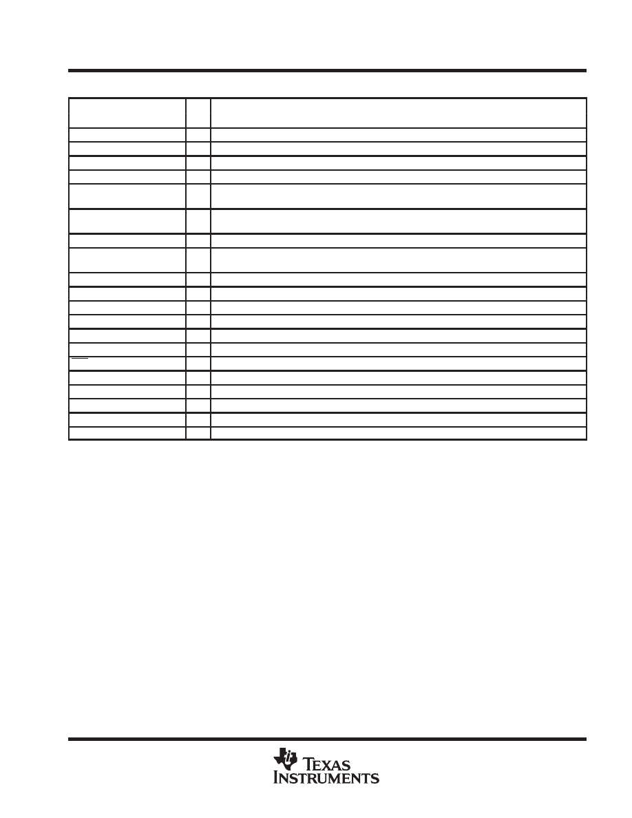
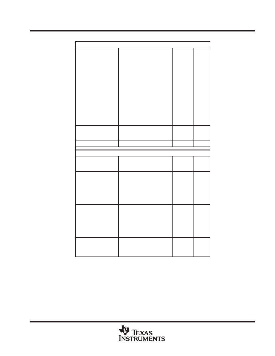
Terminal Functions
TERMINAL
TERMINAL
I/O
DESCRIPTION
NAME
NO.
I/O
DESCRIPTION
P1.0/TACLK
13
I/O
General-purpose digital I/O pin/Timer_A, clock signal TACLK input
P1.1/TA0
14
I/O
General-purpose digital I/O pin/Timer_A, capture: CCI0A input, compare: Out0 output
P1.2/TA1
15
I/O
General-purpose digital I/O pin/Timer_A, capture: CCI1A input, compare: Out1 output
P1.3/TA2
16
I/O
General-purpose digital I/O pin/Timer_A, capture: CCI2A input, compare: Out2 output
P1.4/SMCLK/TCK
17
I/O
General-purpose digital I/O pin/SMCLK signal output/test clock, input terminal for device programming
and test
P1.5/TA0/TMS
18
I/O
General-purpose digital I/O pin/Timer_A, compare: Out0 output/test mode select, input terminal for
device programming and test
P1.6/TA1/TDI
19
I/O
General-purpose digital I/O pin/Timer_A, compare: Out1 output/test data input terminal
P1.7/TA2/TDO/TDI†
20
I/O
General-purpose digital I/O pin/Timer_A, compare: Out2 output/test data output terminal or data input
during programming
P2.0/ACLK
8
I/O
General-purpose digital I/O pin/ACLK output
P2.1/INCLK
9
I/O
General-purpose digital I/O pin/Timer_A, clock signal at INCLK
P2.2/TA0
10
I/O
General-purpose digital I/O pin/Timer_A, capture: CCI0B input, compare: Out0 output
P2.3/TA1
11
I/O
General-purpose digital I/O pin/Timer_A, capture: CCI1B input, compare: Out1 output
P2.4/TA2
12
I/O
General-purpose digital I/O pin/Timer_A, compare: Out2 output
P2.5/Rosc
3
I/O
General-purpose digital I/O pin/Input for external resistor that defines the DCO nominal frequency
RST/NMI
7
I
Reset or nonmaskable interrupt input
TEST
1
I
Select of test mode for JTAG pins on Port1. Must be tied low with less than 30 k
Ω
.
VCC
2
Supply voltage
VSS
4
Ground reference
XIN
6
I
Input terminal of crystal oscillator
XOUT/TCLK
5
I/O
Output terminal of crystal oscillator or test clock input
† TDO or TDI is selected via JTAG instruction.
short-form description
processing unit
The processing unit is based on a consistent, and orthogonally-designed CPU and instruction set. This design
structure results in a RISC-like architecture, highly transparent to the application development, and noted for
its programming simplicity. All operations other than program-flow instructions are consequently performed as
register operations in conjunction with seven addressing modes for source and four modes for destination
operands.
MSP430F11x
MIXED SIGNAL MICROCONTROLLER
SLAS256B – NOVEMBER 1999 – REVISED JUNE 2000
4
POST OFFICE BOX 655303
•
DALLAS, TEXAS 75265
short-form description (continued)
CPU
All sixteen registers are located inside the CPU,
providing reduced instruction execution time. This
reduces a register-register operation execution
time to one cycle of the processor.
Four registers are reserved for special use as a
program counter, a stack pointer, a status register,
and a constant generator. The remaining twelve
registers are available as general-purpose
registers.
Peripherals are connected to the CPU using a
data address and control buses and can be
handled easily with all instructions for memory
manipulation.
instruction set
The instructions set for this register-register architecture provides a powerful and easy-to-use assembly
language. The instruction set consists of 51 instructions with three formats and seven addressing modes.
Table 1 provides a summation and example of the three types of instruction formats; the addressing modes are
listed in Table 2.
Table 1. Instruction Word Formats
Dual operands, source-destination
e.g. ADD R4, R5
R4 + R5
→
R5
Single operands, destination only
e.g. CALL R8
PC
→
(TOS), R8
→
PC
Relative jump, un-/conditional
e.g. JNE
Jump-on equal bit = 0
Most instructions can operate on both word and byte data. Byte operations are identified by the suffix B.
Examples:
Instructions for word operation
Instructions for byte operation
MOV
EDE,TONI
MOV.B
EDE,TONI
ADD
#235h,&MEM
ADD.B
#35h,&MEM
PUSH
R5
PUSH.B
R5
SWPB
R5
—
Table 2. Address Mode Descriptions
ADDRESS MODE
s
d
SYNTAX
EXAMPLE
OPERATION
Register
√
√
MOV Rs, Rd
MOV R10, R11
R10
→
R11
Indexed
√
√
MOV X(Rn), Y(Rm)
MOV 2(R5), 6(R6)
M(2 + R5)
→
M(6 + R6)
Symbolic (PC relative)
√
√
MOV EDE, TONI
M(EDE)
→
M(TONI)
Absolute
√
√
MOV &MEM, &TCDAT
M(MEM)
→
M(TCDAT)
Indirect
√
MOV @Rn, Y(Rm)
MOV @R10, Tab(R6)
M(R10)
→
M(Tab + R6)
Indirect autoincrement
√
MOV @Rn+, RM
MOV @R10+, R11
M(R10)
→
R11, R10 + 2
→
R10
Immediate
√
MOV #X, TONI
MOV #45, TONI
#45
→
M(TONI)
NOTE: s = source d = destination Rs/Rd = source register/destination register Rn = register number
Program Counter
General-Purpose Register
PC/R0
Stack Pointer
SP/R1
Status Register
SR/CG1/R2
Constant Generator
CG2/R3
R4
General-Purpose Register
R5
General-Purpose Register
R14
General-Purpose Register
R15
MSP430F11x
MIXED SIGNAL MICROCONTROLLER
SLAS256B – NOVEMBER 1999 – REVISED JUNE 2000
5
POST OFFICE BOX 655303
•
DALLAS, TEXAS 75265
instruction set (continued)
Computed branches (BR) and subroutine calls (CALL) instructions use the same addressing modes as the other
instructions. These addressing modes provide
indirect addressing, ideally suited for computed branches and
calls. The full use of this programming capability permits a program structure different from conventional 8- and
16-bit controllers. For example, numerous routines can easily be designed to deal with pointers and stacks
instead of using flag type programs for flow control.
operation modes and interrupts
The MSP430 operating modes support various advanced requirements for ultralow-power and ultralow energy
consumption. This is achieved by the intelligent management of the operations during the different module
operation modes and CPU states. The advanced requirements are fully supported during interrupt event
handling. An interrupt event awakens the system from each of the various operating modes and returns with
the
RETI instruction to the mode that was selected before the interrupt event. The different requirements of the
CPU and modules, which are driven by system cost and current consumption objectives, necessitate the use
of different clock signals:
D
Auxiliary clock ACLK (from LFXT1CLK/crystal’s frequency), used by the peripheral modules
D
Main system clock MCLK, used by the CPU and system
D
Subsystem clock SMCLK, used by the peripheral modules
low-power consumption capabilities
The various operating modes are controlled by the software through the operation of the internal clock system.
This clock system provides many combinations of hardware and software capabilities to run the application with
the lowest power consumption and with optimized system costs:
D
Use the internal clock (DCO) generator without any external components.
D
Select an external crystal or ceramic resonator for lowest frequency or cost.
D
Select and activate the proper clock signals (LFXT1CLK and/or DCOCLK) and clock pre-divider function.
D
Apply an external clock source.
Four of the control bits that influence the operation of the clock system and support fast turnon from low power
operating modes are located in the status register SR. The four bits that control the CPU and the system clock
generator are SCG1, SCG0, OscOff, and CPUOff:
status register R2
Reserved For Future
Enhancements
15
9
8
7
0
V
SCG1
SCG0
OscOff
CPUOff
GIE
N
Z
C
rw-0
rw-0
rw-0
rw-0
rw-0
rw-0
rw-0
rw-0
rw-0
rw-0
6
5
4
3
2
1
The bits CPUOff, SCG1, SCG0, and OscOff are the most important low-power control bits when the basic
function of the system clock generator is established. They are pushed onto the stack whenever an interrupt
is accepted and thereby saved so that the previous mode of operation can be retrieved after the interrupt
request. During execution of an interrupt handler routine, the bits can be manipulated via indirect access of the
data on the stack. That allows the program to resume execution in another power operating mode after the
return from interrupt (RETI).
SCG1:
The clock signal SMCLK, used for peripherals, is enabled when bit SCG1 is reset or disabled if
the bit is set.
MSP430F11x
MIXED SIGNAL MICROCONTROLLER
SLAS256B – NOVEMBER 1999 – REVISED JUNE 2000
6
POST OFFICE BOX 655303
•
DALLAS, TEXAS 75265
SCG0:
The dc-generator is active when SCG0 is reset. The dc-generator can be deactivated only if the
SCG0 bit is set and the DCOCLK signal is not used for MCLK or SMCLK. The current consumed
by the dc-generator defines the basic frequency of the DCOCLK. It is a dc current.
The clock signal DCOCLK is deactivated if it is not used for MCLK or SMCLK or if the SCG0 bit
is set. There are two situations when the SCG0 bit cannot switch off the DCOCLK signal:
1. DCOCLK frequency is used for MCLK (CPUOff=0 and SELM.1=0).
2. DCOCLK frequency is used for SMCLK (SCG1=0 and SELS=0).
NOTE:
When the current is switched off (SCG0=1) the start of the DCOCLK is delayed slightly. The delay
is in the
µ
s-range (see device parameters for details).
OscOff:
The LFXT1 crystal oscillator is active when the OscOff bit is reset. The LFXT1 oscillator can only
be deactivated if the OscOff bit is set and it is not used for MCLK or SMCLK. The setup time to
start a crystal oscillation needs consideration when the oscillator off option is used. Mask
programmable (ROM) devices can disable this feature so that the oscillator can never be switched
off by software.
CPUOff:
The clock signal MCLK, used for the CPU, is active when the CPUOff bit is reset or stopped if it
is set.
interrupt vector addresses
The interrupt vectors and the power-up starting address are located in the memory with an address range of
0FFFFh-0FFE0h. The vector contains the 16-bit address of the appropriate interrupt handler instruction
sequence.
INTERRUPT SOURCE
INTERRUPT FLAG
SYSTEM INTERRUPT
WORD ADDRESS
PRIORITY
Power-up, external reset,
watchdog
WDTIFG (Note1)
KEYV (Note 1)
Reset
0FFFEh
15, highest
NMI, oscillator fault, flash
memory access violation
NMIIFG (Notes 1 and 5)
OFIFG (Notes 1 and 5)
ACCVIFG (Notes 1 and 5)
(non)-maskable,
(non)-maskable,
(non)-maskable
0FFFCh
14
0FFFAh
13
0FFF8h
12
0FFF6h
11
Watchdog timer
WDTIFG
maskable
0FFF4h
10
Timer_A
CCIFG0 (Note 2)
maskable
0FFF2h
9
Timer_A
CCIFG1, CCIFG2, TAIFG (Notes 1 and 2)
maskable
0FFF0h
8
0FFEEh
7
0FFECh
6
0FFEAh
5
0FFE8h
4
I/O Port P2 (eight flags – see
Note 3)
P2IFG.0 to P2IFG.7 (Notes 1 and 2)
maskable
0FFE6h
3
I/O Port P1 (eight flags)
P1IFG.0 to P1IFG.7 (Notes 1 and 2)
maskable
0FFE4h
2
0FFE2h
1
0FFE0h
0, lowest
NOTES:
1. Multiple source flags
2. Interrupt flags are located in the module
3. There are eight Port P2 interrupt flags, but only six Port P2 I/O pins (P2.0–5) are implemented on the 11x devices.
4. Nonmaskable: neither the individual nor the general interrupt enable bit will disable an interrupt event.
5. (non)-maskable: the individual interrupt enable bit can disable an interrupt event, but the general interrupt enable cannot.
MSP430F11x
MIXED SIGNAL MICROCONTROLLER
SLAS256B – NOVEMBER 1999 – REVISED JUNE 2000
7
POST OFFICE BOX 655303
•
DALLAS, TEXAS 75265
special function registers
Most interrupt and module enable bits are collected into the lowest address space. Special function register bits
that are not allocated to a functional purpose are not physically present in the device. Simple software access
is provided with this arrangement.
interrupt enable 1 and 2
7
6
5
4
0
OFIE
WDTIE
3
2
1
rw-0
rw-0
rw-0
Address
0h
NMIIE
ACCVIE
rw-0
WDTIE:
Watchdog timer enable signal
OFIE:
Oscillator fault enable signal
NMIIE:
Nonmaskable interrupt enable signal
ACCVIE:
Access violation at flash memory
7
6
5
4
0
3
2
1
Address
01h
interrupt flag register 1 and 2
7
6
5
4
0
OFIFG
WDTIFG
3
2
1
rw-0
rw-1
rw-0
Address
02h
NMIIFG
WDTIFG:
Set on overflow or security key violation or
Reset on V
CC
power-on or reset condition at RST/NMI-pin
OFIFG:
Flag set on oscillator fault
NMIIFG:
Set via RST/NMI-pin
7
6
5
4
0
3
2
1
Address
03h
Legend
rw:
rw-0:
Bit can be read and written.
Bit can be read and written. It is reset by PUC.
SFR bit is not present in device.
MSP430F11x
MIXED SIGNAL MICROCONTROLLER
SLAS256B – NOVEMBER 1999 – REVISED JUNE 2000
8
POST OFFICE BOX 655303
•
DALLAS, TEXAS 75265
memory organization
01FFh
MSP430F112
Int. Vector
1 KB Flash
Segment0,1
128B RAM
16b Per.
8b Per.
SFR
FFDFh
FC00h
027Fh
0200h
0100h
00FFh
0010h
000Fh
0000h
MSP430F110
1 KB
Boot ROM
128B Flash
SegmentA
10FFh
1080h
0C00h
0FFFh
FFFFh
FFE0h
Int. Vector
4 KB
Flash
Segment0–7
256B RAM
16b Per.
8b Per.
SFR
FFFFh
FFE0h
FFDFh
02FFh
0200h
0100h
00FFh
0010h
000Fh
0000h
F000h
Main
Memory
10FFh
2
×
128B
Flash
SegmentA,B
Information
Memory
1000h
1 KB
Boot ROM
0FFFh
0C00h
01FFh
boot ROM containing bootstrap loader
The intention of the bootstrap loader is to download data into the flash memory module. Various write, read, and
erase operations are needed for a proper download environment. The bootstrap loader is only available on F
devices.
functions of the bootstrap loader:
Definition of read:
apply and transmit data of peripheral registers or memory to pin P1.1 (BSLTX)
write:
read data from pin P2.2 (BSLRX) and write them into flash memory
unprotected functions
Mass erase, erase of the main memory (Segment0 to Segment7)
Access to the MSP430 via the bootstrap loader is protected. It must be enabled before any protected function
can be performed. The 256 bits in 0FFE0h to 0FFFFh provide the access key.
protected functions
All protected functions can be executed only if the access is enabled.
D
Write/program byte into flash memory; parameters passed are start address and number of bytes (the
segment-write feature of the flash memory is not supported and not useful with the UART protocol).
D
Segment erase of Segment0 to Segment7 in the main memory and segment erase of SegmentA and
SegmentB in the information memory.
D
Read all data in main memory and information memory.
D
Read and write to all byte-peripheral modules and RAM.
D
Modify PC and start program execution immediately.
NOTE:
Unauthorized readout of code and data is prevented by the user’s definition of the data in the
interrupt memory locations.
MSP430F11x
MIXED SIGNAL MICROCONTROLLER
SLAS256B – NOVEMBER 1999 – REVISED JUNE 2000
9
POST OFFICE BOX 655303
•
DALLAS, TEXAS 75265
boot ROM containing bootstrap loader (continued)
features of the bootstrap loader are:
D
UART communication protocol, fixed to 9600 baud
D
Port pin P1.1 for transmit, P2.2 for receive
D
TI standard serial protocol definition
D
Implemented in flash memory version only
D
Program execution starts with the user vector at 0FFFEh or with the bootstrap loader (start vector is at
address 0C00h)
hardware resources used for serial input/output:
D
Pins P1.1 and P2.2 for serial data transmission
D
Test and RST/NMI to start program execution at the reset or bootstrap loader vector
D
Basic clock module:
Rsel=5, DCO=4, MOD=0, DCOCLK for MCLK and SMCLK, clock divider for MCLK
and SMCLK at default: dividing by 1
D
Timer_A: Timer_A operates in continuous mode with MCLK source selected, input divider set to 1, using
CCR0, and polling of CCIFG0.
D
WDT:
Watchdog timer is halted
D
Interrupt: GIE=0, NMIIE=0, OFIFG=0, ACCVIFG=0
D
Memory allocation and stack pointer:
If the stack pointer points to RAM addresses above 0220h, 6 bytes of the stack are allocated
plus RAM addresses 0200h to 0219h. Otherwise the stack pointer is set to 0220h and allocates
RAM from 0200h to 021Fh.
NOTE:
When writing RAM data via bootstrap loader, make sure that the stack is outside the range of the
data being written.
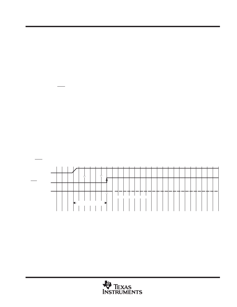
Program execution begins with the user’s reset vector at FFFEh (standard method) if TEST is held low while
RST/NMI goes from low to high:
RST/NMI PIN
TEST PIN
User Program Starts
VCC
Reset Condition
MSP430F11x
MIXED SIGNAL MICROCONTROLLER
SLAS256B – NOVEMBER 1999 – REVISED JUNE 2000
10
POST OFFICE BOX 655303
•
DALLAS, TEXAS 75265
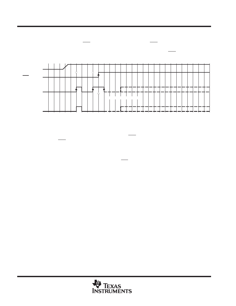
boot ROM containing bootstrap loader (continued)
Program execution begins with the bootstrap vector at 0C00h (boot ROM) if a minimum of two positive edges
have been applied to TEST while RST/NMI is low, and TEST is high when RST/NMI goes from low to high. The
TEST signal is normally used internally to switch pins P1.4, P1.5, P1.6, and P1.7 between their application
function and the JTAG function. If the second rising edge at TEST is applied while RST/NMI is held low, the
internal TEST signal is held low and the pins remain in the application mode:
RST/NMI PIN
TEST
(Internal)
TEST PIN
Bootstrap Loader Starts
VCC
Test mode can be entered again after TEST is taken low and then back high.
The bootstrap loader will not be started (via the vector in address 0C00h), if:
D
There were less than two positive edges at TEST while RST/NMI is low
D
TEST is low if RST/NMI goes from low to high
D
JTAG has control over the MSP430 resources
D
Supply voltage V
CC
drops and a POR is executed
WARNING:
The bootstrap loader starts correctly only if the RST/NMI pin is in reset mode. If it is switched
to the NMI function, unpredictable program execution may result. However, a
bootstrap-load may be started using software and the bootstrap vector, for example the
instruction BR &0C00h.
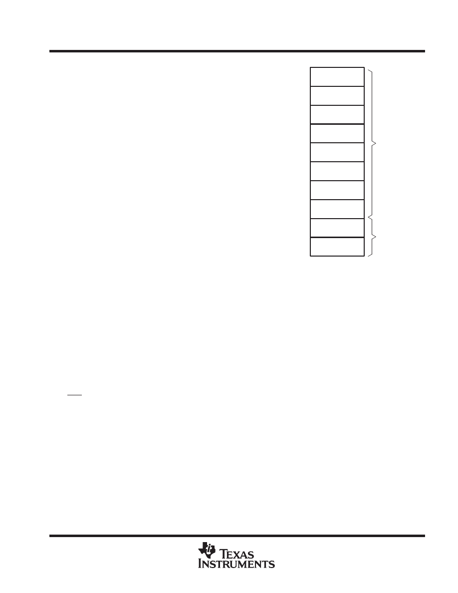
Segment0 w/
Interrupt Vectors
0FFFFh
0FE00h
Information
Memory
Flash Main Memory
Segment1
Segment2
Segment3
Segment4
Segment5
Segment6
Segment7
SegmentA
SegmentB
0FDFFh
0FC00h
0FBFFh
0FA00h
0F9FFh
0F800h
0F7FFh
0F600h
0F5FFh
0F400h
0F3FFh
0F200h
0F1FFh
0F000h
010FFh
01080h
0107Fh
01000h
NOTE: All segments not implemented on all devices.
MSP430F11x
MIXED SIGNAL MICROCONTROLLER
SLAS256B – NOVEMBER 1999 – REVISED JUNE 2000
11
POST OFFICE BOX 655303
•
DALLAS, TEXAS 75265
flash memory
The flash memory consists of 512-byte segments
in the main memory and 128-byte segments in the
information memory. See device memory maps
for specific device information.
Segment0 to Segment7 can be erased individual-
ly, or altogether as a group.
SegmentA and SegmentB can be erased
individually, or as a group with segments 0–7.
The memory in SegmentA and SegmentB is also
called
Information Memory.
V
PP
is generated internally. V
CC
current increases
during programming.
During program/erase cycles, V
CC
must not drop
below the minimum specified for program/erase
operation.
Program and erase timings are controlled by the
flash timing generator—no software intervention
is needed. The input frequency of the flash timing
generator should be in the proper range and must
be applied until the write/program or erase
operation is completed.
During program or erase, no code can be executed from flash memory and all interrupts must be disabled by
setting the GIE, NMIE, ACCVIE, and OFIE bits to zero. If a user program requires execution concurrent with
a flash program or erase operation, the program must be executed from memory other than the flash memory
(e.g., boot ROM, RAM). In the event a flash program or erase operation is initiated while the program counter
is pointing to the flash memory, the CPU will execute JMP $ instructions until the flash program or erase
operation is completed. Normal execution of the previously running software then resumes.
Unprogrammed, new devices may have some bytes programmed in the information memory (needed for test
during manufacturing). The user should perform an erase of the information memory prior to first use.
flash memory control register FCTL1
All control bits are reset during PUC. PUC is active after V
CC
is applied, a reset condition is applied to the
RST/NMI pin, the watchdog timer expires, a watchdog access violation occurs, or an improper flash operation
has been performed. A more detailed description of the control-bit functions is found in the flash memory module
description (refer to
MSP430x1xx User’s Guide, literature number SLAU049). Any write to control register
FCTL1 during erase, mass erase, or write (programming) will end in an access violation with ACCVIFG=1.
Special conditions apply for segment-write mode. Refer to
MSP430x1xx User’s Guide, literature number
SLAU049 for details.
MSP430F11x
MIXED SIGNAL MICROCONTROLLER
SLAS256B – NOVEMBER 1999 – REVISED JUNE 2000
12
POST OFFICE BOX 655303
•
DALLAS, TEXAS 75265
flash memory control register FCTL1 (continued)
Read access is possible at any time without restrictions.
The control bits of control register FCTL1 are:
SEG
WRT
FCTL1
0128h
MEras
Erase
res.
0
r0
rw-0
rw–0
7
rw–0
WRT
rw–0
res.
r0
res.
r0
res.
r0
8
15
FCTL1 read:
096h
FCTL1 write:
0A5h
Erase
0128h, bit1,
Erase a segment
0:
1:
No segment erase will be started.
Erase of one segment is enabled. The segment to be erased is defined by a
dummy write into any address within the segment. The erase bit is
automatically reset when the erase operation is completed.
MEras
0128h, bit2,
Mass Erase, main memory segments are erased together.
0:
1:
No segment erase will be started.
Erase of main memory segments is enabled. Erase starts when a dummy
write to any address in main memory is executed. The MEras bit is
automatically reset when the erase operation is completed.
WRT
0128h, bit6,
Bit WRT must be set for a successful write execution.
If bit WRT is reset and write access to the flash memory is attempted, an
access violation occurs and ACVIFG is set.
SEGWRT
0128h, bit7,
Bit SEGWRT may be used to reduce total programming time.
Refer to
MSP430x1xx User’s Guide, literature number SLAU049 for details.
0:
1:
No segment-write acceleration is selected.
Segment-write is used. This bit needs to be reset and set between segment
borders.
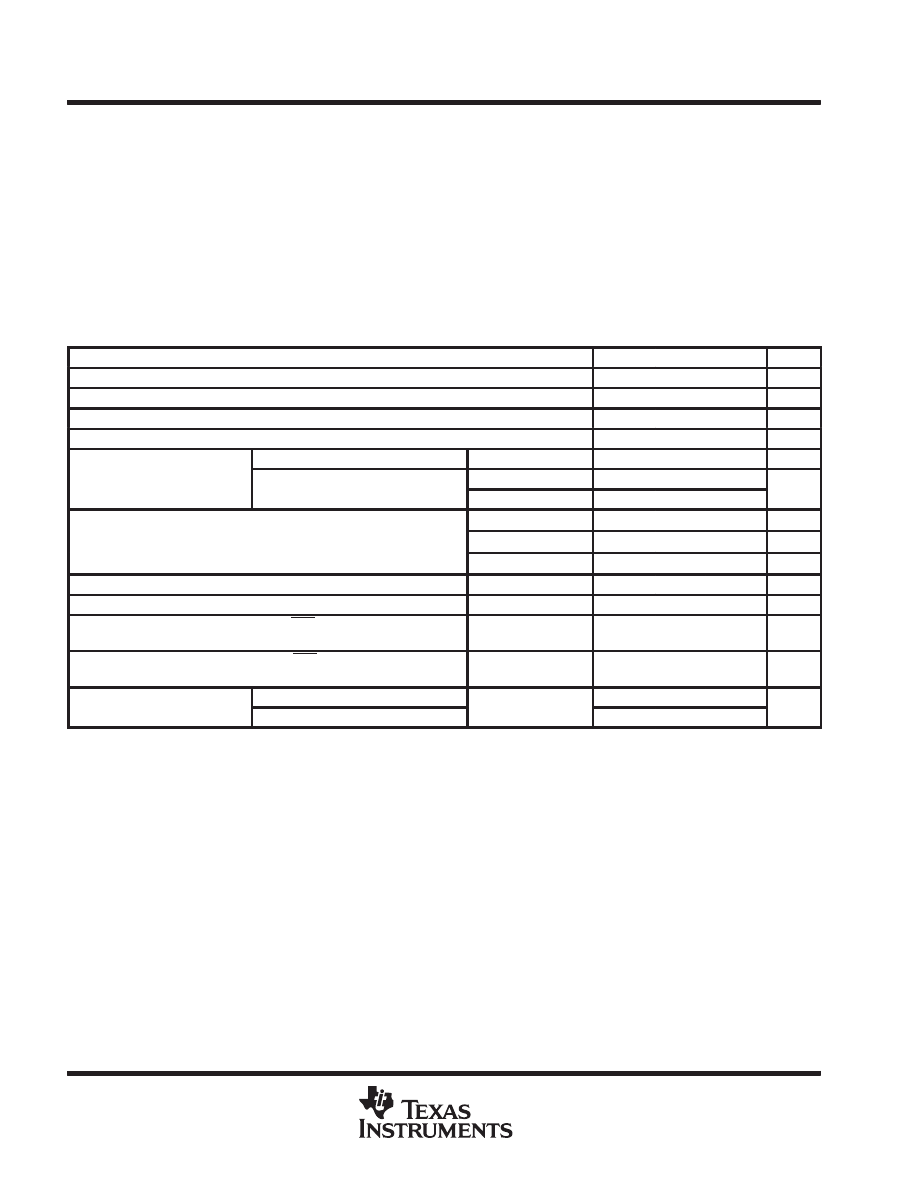
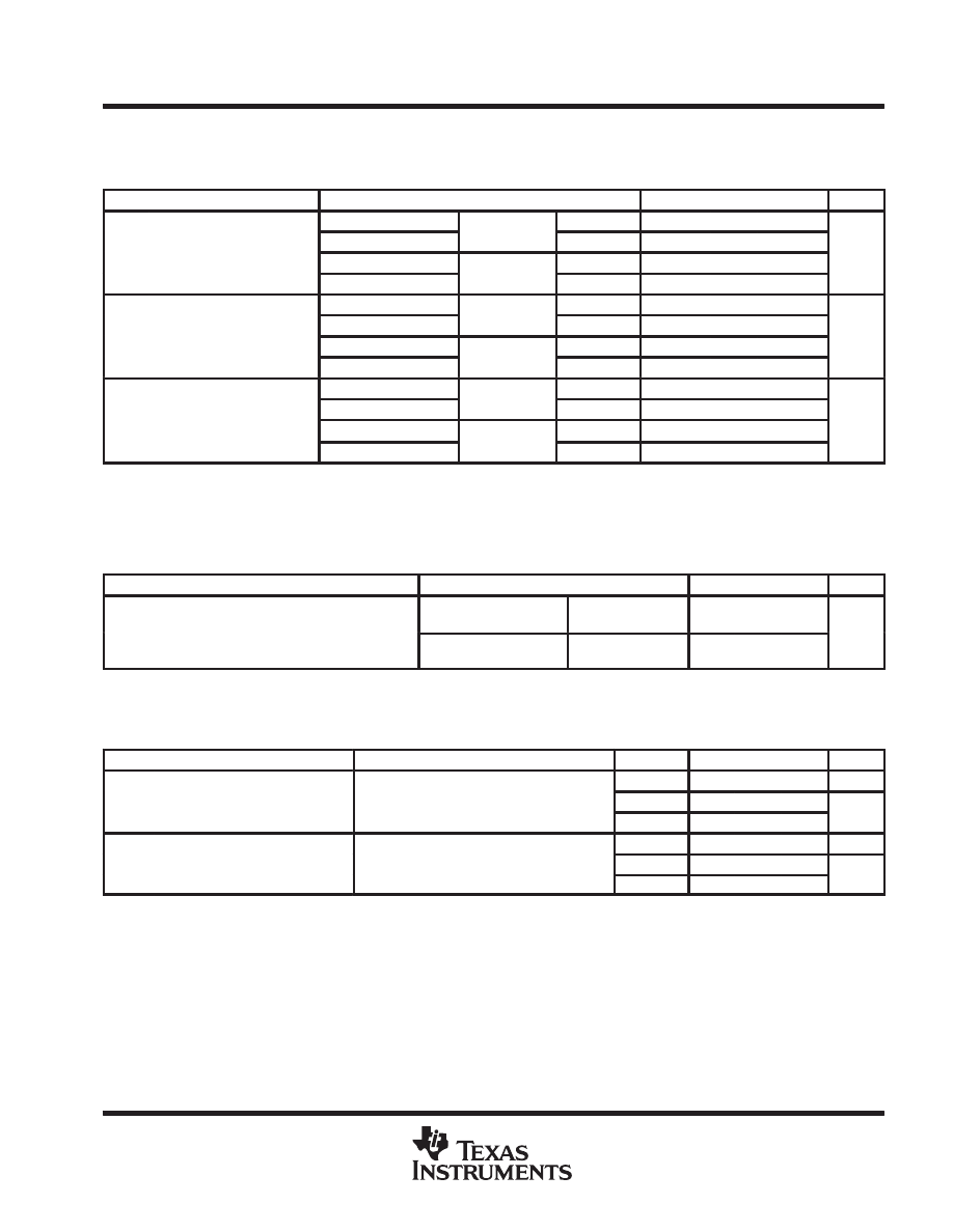
Table 3. Allowed Combinations of Control Bits Allowed for Flash Memory Access
FUNCTION PERFORMED
SEGWRT
WRT
MEras
Erase
BUSY
WAIT
Lock
Write word or byte
0
1
0
0
0
0
0
Write word or byte in same segment, segment write mode
1
1
0
0
0
→
1
0
→
1
0
Erase one segment by writing to any address in the target segment
0
0
0
1
0
0
0
Erase all segments (0 to 7) but not the information memory
(segments A and B)
0
0
1
0
0
0
0
Erase all segments (0 to 7 and A and B) by writing to any address in
the flash memory module
0
0
1
1
0
0
0
NOTE: The table shows all valid combinations. Any other combination will result in an access violation.
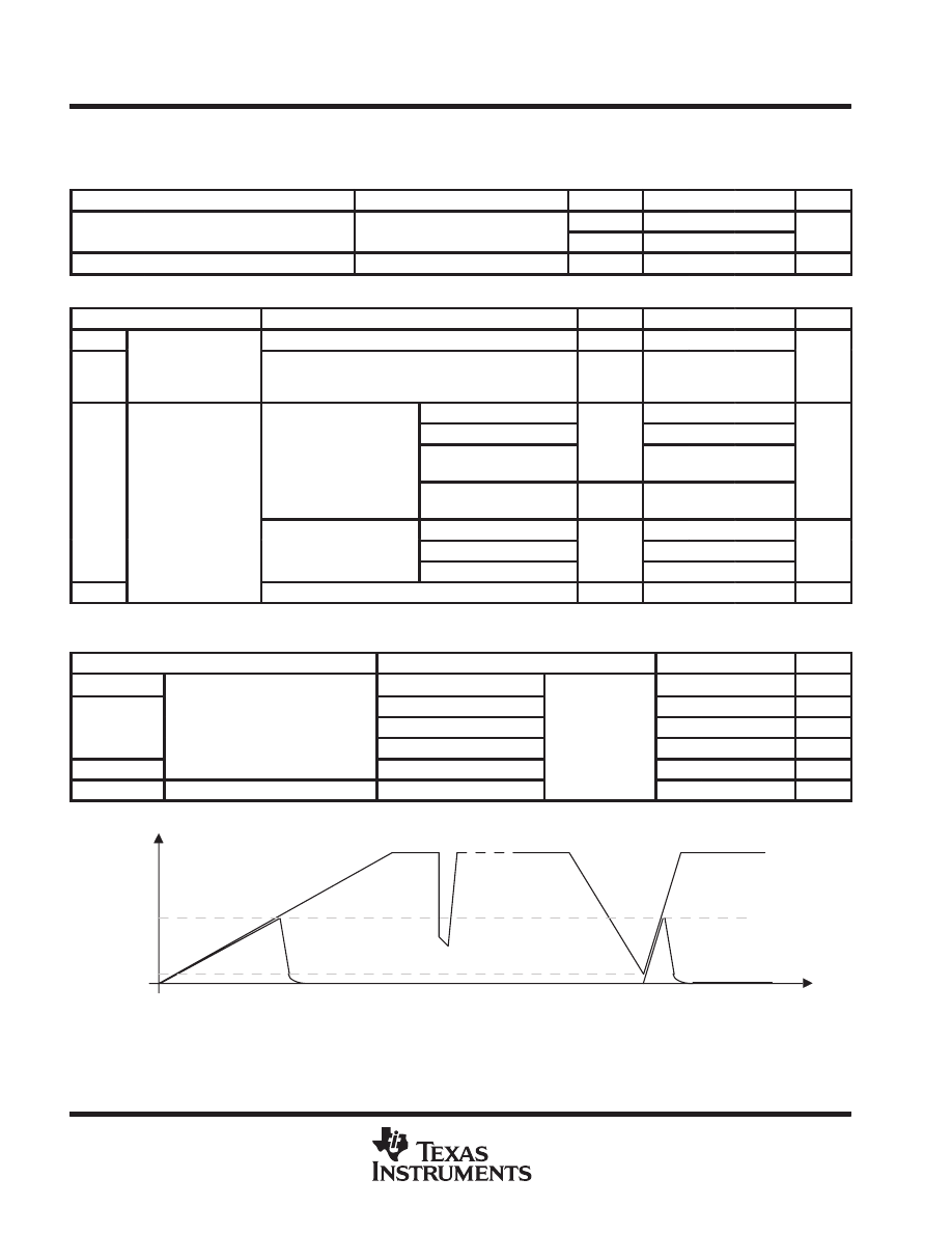
flash memory, timing generator, control register FCTL2
The timing generator (Figure 1) generates all the timing signals necessary for write, erase, and mass erase from
the selected clock source. One of three different clock sources may be selected by control bits SSEL0 and
SSEL1 in control register FCTL2. The selected clock source should be divided to meet the frequency
requirements specified in the recommended operating conditions.
MSP430F11x
MIXED SIGNAL MICROCONTROLLER
SLAS256B – NOVEMBER 1999 – REVISED JUNE 2000
13
POST OFFICE BOX 655303
•
DALLAS, TEXAS 75265
flash memory, timing generator, control register FCTL2 (continued)
The flash timing generator is reset with PUC. It is also reset if the emergency exit bit EMEX is set.
Control register FCTL2 may not be written to if the BUSY bit is set; otherwise, an access violation will occur
(ACCVIFG=1).
Read access is possible at any time without restrictions.
ACLK
0
1
2
3
SSEL1
MCLK
SMCLK
SMCLK
Divider,
1 .. 64
Reset
Flash Timing
Generator
SSEL0
FN5.......... FN0
fX
PUC
EMEX
BUSY
WAIT
Write ’1’ to
Figure 1. Flash Memory Timing Generator Diagram
FCTL2
012Ah
FN2
FN1
FN0
0
rw-0
rw-1
rw–0
7
rw–0
SSEL0
rw–1
FN5
FN4
FN3
15
FCTL2 read:
096h
FCTL2 write:
0A5h
rw-0
rw-0
rw-0
8
SSEL1
The control bits are:
FN0–FN5
012Ah, bit0–5
These six bits define the division rate of the clock signal. The division
rate is 1 to 64, according to the digital value of FN5 to FN0 plus one.
SSEL0, SSEL1
012Ah, bit6,7
Clock source select
0: ACLK
1: MCLK
2: SMCLK
3: SMCLK
The flash timing generator is reset with PUC. It is also reset if the EMEX bit is set.
flash memory control register FCTL3
There are no restrictions to modify this control register.
FCTL3
012Ch
KEYV
BUSY
0
r(w)-0
rw-(0)
rw–0
7
r0
res.
r0
EMEX
Lock
WAIT
15
FCTL3 read:
096h
FCTL3 write:
0A5h
rw-1
rw-1
rw-0
8
ACCV
IFG
res.

MSP430F11x
MIXED SIGNAL MICROCONTROLLER
SLAS256B – NOVEMBER 1999 – REVISED JUNE 2000
14
POST OFFICE BOX 655303
•
DALLAS, TEXAS 75265
flash memory control register FCTL3 (continued)
BUSY
012Ch, bit0,
The BUSY bit shows if an access to the flash memory is allowed (BUSY=0), or
if an access violation occurs. The BUSY bit is read-only, but a write operation is
allowed. The BUSY bit should be tested before each write and erase cycle. The
flash timing-generator hardware immediately sets the BUSY bit after start of a
write, segment-write, erase, or
mass erase operation. If the timing generator has
completed the operation, the BUSY bit is reset by the hardware.
No program code can be executed from the
busy flash memory during the entire
program or erase cycle.
0:
Flash memory is not busy.
1:
Flash memory is busy, and remains in busy state if segment write function
is in
wait mode.
KEYV,
012Ch, bit1
Key violation
0:
Key 0A5h (high byte) was not violated.
1:
Key 0A5h (high byte) was violated. Violation occurs when a write access to
registers FCTL1, FCTL2, or FCTL3 is executed and the
high byte is not
equal to 0A5h. If the security key is violated, bit KEYV is set and a PUC is
performed.
ACCVIFG,
012Ch, bit2
Access violation interrupt flag
The access-violation flag is set when any combination of control bits other than
those shown in Table 3 is attempted, or an instruction is fetched while a
segment-write operation is active.
Reading the control registers will not set the ACCVIFG bit.
NOTE: The respective interrupt-enable bit ACCVIE is located in the interrupt
enable register IE1 in the special function register. The software can set
the ACCVIFG bit. If set by software, an NMI is also executed.
WAIT,
012CH, bit3
In the segment-write mode, the WAIT bit indicates that data has been written and
the flash memory is prepared to receive the next data for programming. The
WAIT bit is read only, but a write to the WAIT bit is allowed.
0:
The segment-write operation has began and programming is in progress.
1:
The segment-write operation is active and data programming is complete.

MSP430F11x
MIXED SIGNAL MICROCONTROLLER
SLAS256B – NOVEMBER 1999 – REVISED JUNE 2000
15
POST OFFICE BOX 655303
•
DALLAS, TEXAS 75265
flash memory control register FCTL3 (continued)
LOCK
012Ch, bit4,
The lock bit may be set during any write, segment-erase, or
mass-erase request.
Any active sequence in progress is completed normally. In segment-write mode,
the SEGWRT bit is reset and the WAIT bit is set after the mode ends. The lock
bit is controlled by software or hardware. If an access violation occurs and the
ACCVIFG is set, the LOCK bit is set automatically.
0:
Flash memory may be read, programmed, erased, or
mass erased.
1:
Flash memory may be read but not programmed, erased, or
mass erased.
A current program, erase, or
mass-erase operation will complete normally.
The access-violation interrupt flag ACCVIFG is set when data are written to
the flash memory module while the lock bit is set.
EMEX,
012Ch, bit5,
Emergency exit. The emergency exit should only be used if the flash memory
write or erase operation is out of control.
0:
No function
1:
Stops the active operation immediately, and shuts down all internal parts in
the flash memory controller. Current consumption immediately drops back
to the active mode. All bits in control register FCTL1 are reset. Since the
EMEX bit is automatically reset by hardware, the software always reads
EMEX as 0.
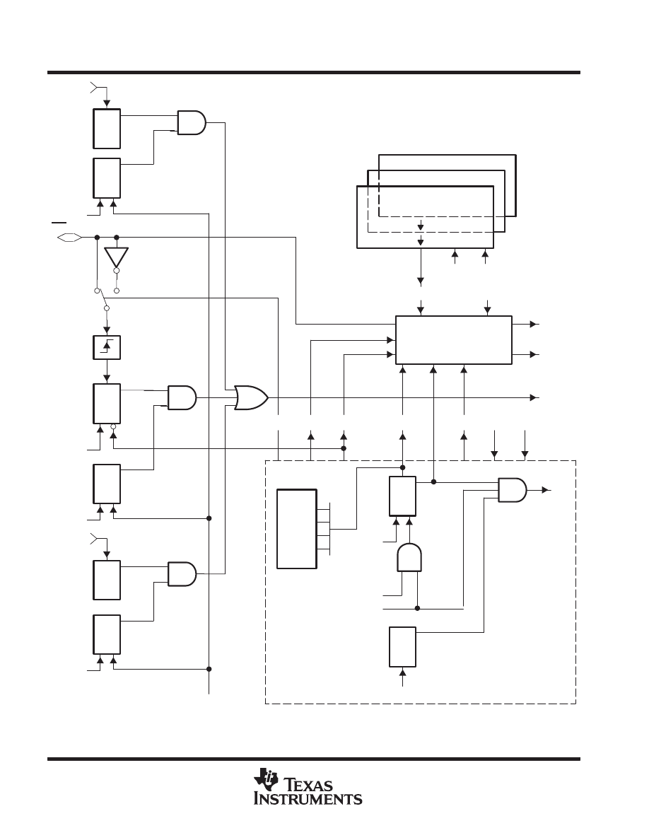
flash memory, interrupt and security key violation
One NMI vector is used for three NMI events: RST/NMI (NMIIFG), oscillator fault (OFIFG), and flash-memory
access violation (ACCVIFG). The software can determine the source of the interrupt request since all flags
remain set until they are reset by software. The enable flag(s) should be set simultaneously with one instruction
before the return-from-interrupt RETI instruction. This ensures that the stack remains under control. A pending
NMI interrupt request will not increase stack demand unnecessarily.
MSP430F11x
MIXED SIGNAL MICROCONTROLLER
SLAS256B – NOVEMBER 1999 – REVISED JUNE 2000
16
POST OFFICE BOX 655303
•
DALLAS, TEXAS 75265
Flash Module
Flash Module
Flash Module
KEYV
System Reset
Generator
VCC
POR
PUC
WDTQn
EQU
PUC
POR
PUC
POR
NMIRS
Clear
S
WDTIFG
IRQ
WDTIE
Clear
IE1.0
PUC
POR
IRQA
TIMSEL
Counter
IFG1.0
NMI
TMSEL
NMIES
Watchdog Timer Module
Clear
S
IFG1.4
PUC
Clear
IE1.4
PUC
NMIFG
NMIIE
S
IFG1.1
Clear
IE1.1
PUC
OFIFG
OFIF
OSCFault
NMI_IRQA
IRQA: Interrupt Request Accepted
RST/NMI
S
FCTL1.1
Clear
IE1.5
ACCVIFG
ACCVIE
PUC
ACCV
WDT
Figure 2. Block Diagram of NMI Interrupt Sources

MSP430F11x
MIXED SIGNAL MICROCONTROLLER
SLAS256B – NOVEMBER 1999 – REVISED JUNE 2000
17
POST OFFICE BOX 655303
•
DALLAS, TEXAS 75265
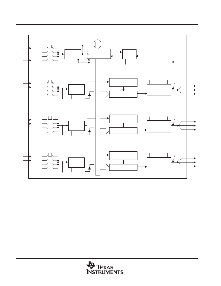
peripherals
Peripherals are connected to the CPU through data, address, and control buses, and they can be handled easily
with memory manipulation instructions.
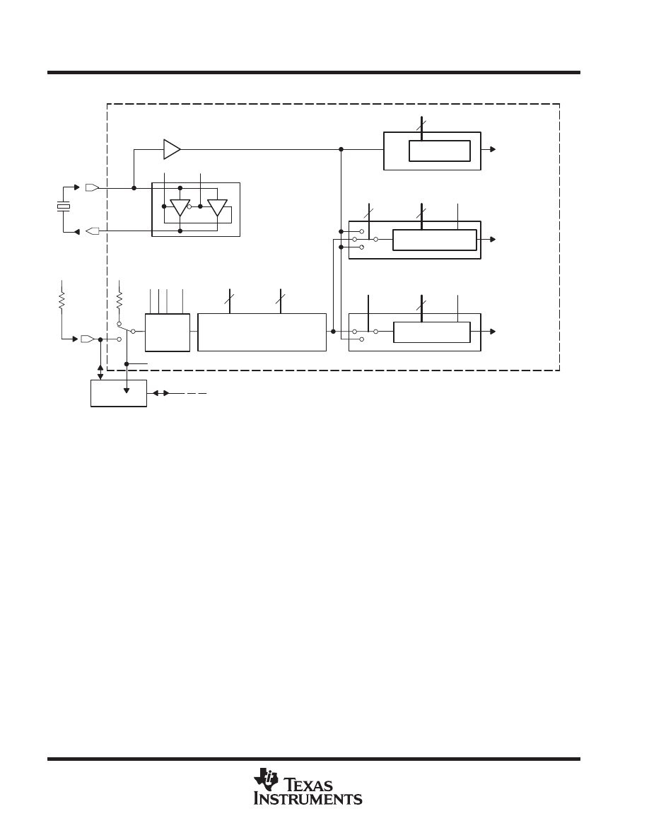
oscillator and system clock
Three clocks are used in the system—the system (master) clock MCLK, the subsystem (master) clock SMCLK,
and the auxiliary clock ACLK:
Main system clock MCLK, used by the CPU and the system
Subsystem clock SMCLK, used by the peripheral modules
Auxiliary clock ACLK, originated by LFXT1CLK (crystal frequency) and used by the peripheral modules
After a POR, the DCOCLK is used by default, the DCOR bit is reset, and the DCO is set to the nominal initial
frequency. Additionally, if LFXT1CLK fails as the source for MCLK, the DCOCLK is automatically selected to
ensure fail-safe operation.
SMCLK can be generated from LFXT1CLK or DCOCLK. ACLK is always generated from LFXT1CLK.
The crystal oscillator can be defined to operate with watch crystals (32768 Hz) or with higher-frequency ceramic
resonators or crystals. The crystal or ceramic resonator is connected across two terminals. No external
components are required for watch-crystal operation. If the high frequency XT1 mode is selected, external
capacitors from XIN to V
SS
and XOUT to V
SS
are required as specified by the crystal manufacturer.
The LFXT1 oscillator starts after applying V
CC
. If the OscOff bit is set to 1, the oscillator stops when it is not used
for MCLK. The clock signals ACLK and SMCLK may be used externally via port pins.
Different application requirements and system conditions dictate different system clock requirements, including:
High frequency for quick reaction to system hardware requests or events
Low frequency to minimize current consumption, EMI, etc.
Stable peripheral clock for timer applications, such as real-time clock (RTC)
Start-stop operation to be enabled with minimum delay
MSP430F11x
MIXED SIGNAL MICROCONTROLLER
SLAS256B – NOVEMBER 1999 – REVISED JUNE 2000
18
POST OFFICE BOX 655303
•
DALLAS, TEXAS 75265
oscillator and system clock (continued)
DIVA
XIN
LFXT1 OSCILLATOR
ACLK
OSCOff
XTS
/1, /2, /4, /8
2
DIVM
/1, /2, /4, /8, Off
2
2
SELM
CPUOff
Auxiliary Clock
MCLK
Main System Clock
DIVS
/1, /2, /4, /8, Off
2
SELS
SCG1
SMCLK
Subsystem Clock
XOUT
SMCLKGEN
LFXT1CLK
MCLKGEN
ACLKGEN
DCOMOD
DCOCLK
Digital Controlled Oscillator (DCO)
+
Modulator (MOD)
DC
Generator
5
3
DCO
MOD
Rsel SCG0
DCOR
The DCO-Generator is connected to pin P2.5/Rosc if DCOR control bit is set.
The port pin P2.5/Rosc is selected if DCOR control bit is reset (initial state).
P2.5
VCC
VCC
0
1
P2.5/Rosc
3
2
0
1
DCGEN
0,1
Figure 3. Clock Signals
Two clock sources, LFXT1CLK and DCOCLK, can be used to drive the MSP430 system. The LFXT1CLK is
generated from the LFXT1 crystal oscillator. The LFXT1 crystal oscillator can operate in three modes—low
frequency (LF), moderate frequency (XT1), and external input mode. The LFXT1 crystal oscillator may be
switched off when it is not in use.
DCOCLK is generated from the DCO. The nominal DCO frequency is defined by the dc generator and can be
set by one external resistor, or can be set to one of eight values with integrated resistors. Additional adjustments
and modulations of DCOCLK are possible by software manipulation of registers in the DCO module. DCOCLK
is stopped automatically when it is not used by the CPU or peripheral modules. The dc generator can be shut
down with the SCG0 bit to realize additional power savings when DCOCLK is not in use.
NOTE:
The system clock generator always starts with the DCOCLK selected for MCLK (CPU clock) to
ensure proper start of program execution. The software defines the final system clock generation
through control bit manipulation.
digital I/O
There are two eight-bit I/O ports, port P1 and port P2 – implemented (11x parts only have six port P2 I/O signals
available on external pins). Both ports, P1 and P2, have seven control registers to give maximum flexibility of
digital input/output to the application:
•
All individual I/O bits are programmable independently.
•
Any combination of input, output, and interrupt conditions is possible.
•
Interrupt processing of external events is fully implemented for all eight bits of port P1 and for six bits of
port P2.
•
Read/write access to all registers with all instructions

MSP430F11x
MIXED SIGNAL MICROCONTROLLER
SLAS256B – NOVEMBER 1999 – REVISED JUNE 2000
19
POST OFFICE BOX 655303
•
DALLAS, TEXAS 75265
digital I/O (continued)
The seven registers are:
•
Input register
8 bits at port P1/P2
contains information at the pins
•
Output register
8 bits at port P1/P2
contains output information
•
Direction register
8 bits at port P1/P2
controls direction
•
Interrupt edge select
8 bits at port P1/P2
input signal change necessary for interrupt
•
Interrupt flags
8 bits at port P1/P2
indicates if interrupt(s) are pending
•
Interrupt enable
8 bits at port P1/P2
contains interrupt enable bits
•
Selection (Port or Mod.) 8 bits at port P1/P2
determines if pin(s) have port or module function
All these registers contain eight bits. Two interrupt vectors are implemented: one commonly used for any
interrupt event on ports P1.0 to P1.7, and one commonly used for any interrupt event on ports P2.0 to P2.7.
NOTE:
Six bits of port P2, P2.0 to P2.5, are available on external pins – but all control and data bits for port
P2 are implemented.
Watchdog Timer
The primary function of the watchdog timer (WDT) module is to perform a controlled system restart after a
software problem has occurred. If the selected time interval expires, a system reset is generated. If this
watchdog function is not needed in an application, the module can work as an interval timer, which generates
an interrupt after the selected time interval.
The watchdog timer counter (WDTCNT) is a 16-bit up-counter which is not directly accessible by software. The
WDTCNT is controlled through the watchdog timer control register (WDTCTL), which is a 16-bit read/write
register. Writing to WDTCTL is, in both operating modes (watchdog or timer), only possible by using the correct
password in the high-byte. The low-byte stores data written to the WDTCTL. The high-byte must be the
password 05Ah. If any value other than 05Ah is written to the high-byte of the WDTCTL, a system reset PUC
is generated. When the password is read, its value is 069h. This minimizes accidental write operations to the
WDTCTL register. In addition to the watchdog timer control bits, there are two bits included in the WDTCTL
register that configure the NMI pin.
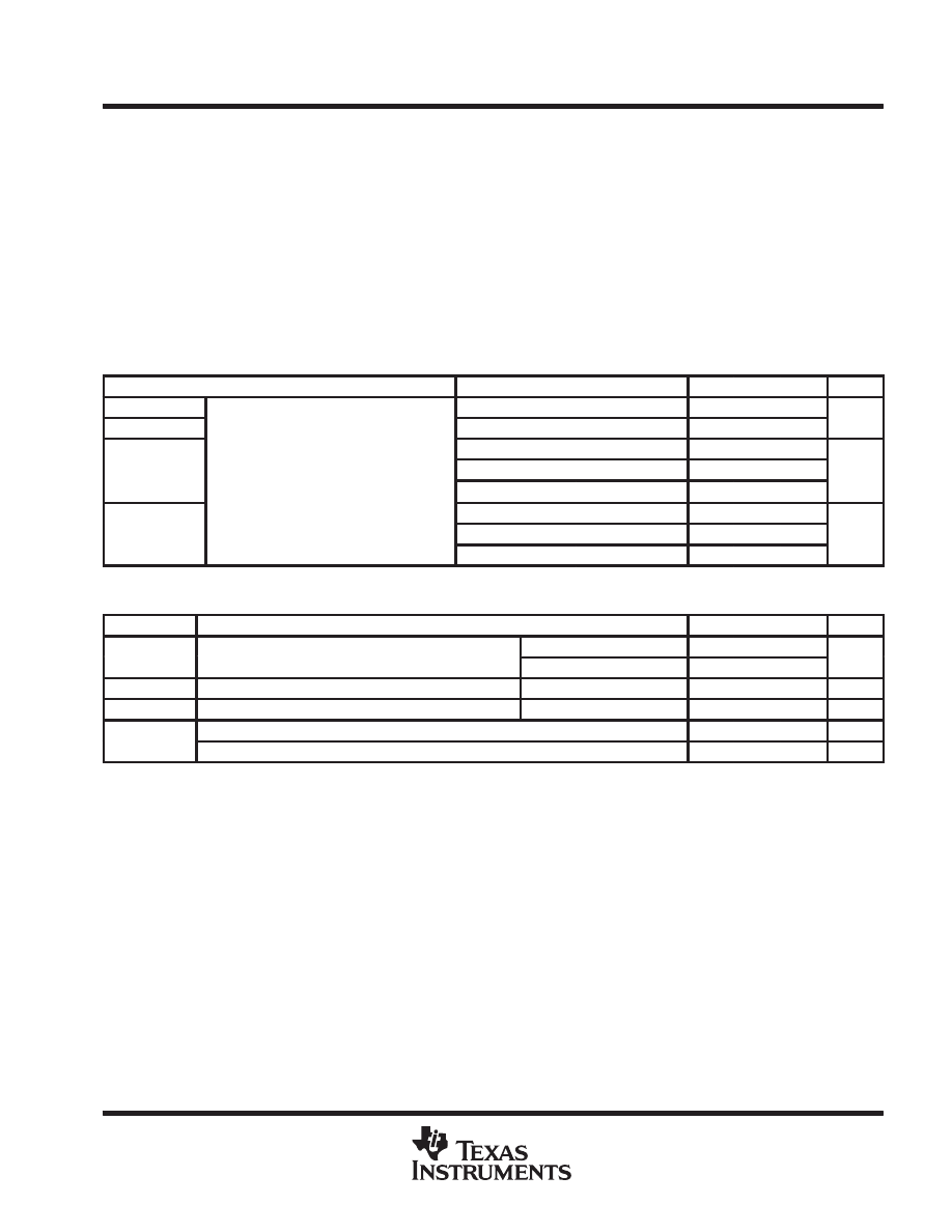
Timer_A (Three capture/compare registers)
The Timer_A module on 11x devices offers one sixteen bit counter and three capture/compare registers. The
timer clock source can be selected to come from two external sources TACLK (SSEL=0) or INCLK (SSEL=3),
or from two internal sources, the ACLK (SSEL=1) or SMCLK (SSEL=2). The clock source can be divided by
one, two, four, or eight. The timer can be fully controlled (in word mode) since it can be halted, read, and written.
It can be stopped, run continuously, counted up or up/down, using one compare block to determine the period.
The three capture/compare blocks are configured by the application to run in capture or compare mode.
The capture mode is primarily used to measure external or internal events using any combination of positive,
negative, or both edges of the signal. Capture mode can be started and stopped by software. Three different
external events TA0, TA1, and TA2 can be selected. At capture/compare register CCR2 the ACLK is the capture
signal if CCI2B is selected. Software capture is chosen if CCISx=2 or CCISx=3 (see Figure 4).
The compare mode is primarily used to generate timings for the software or application hardware, or to generate
pulse-width modulated output signals for various purposes like D/A conversion functions or motor control. An
individual output module is assigned to each of the three capture/compare registers. The output modules can
run independently of the compare function, or can be triggered in several ways.
MSP430F11x
MIXED SIGNAL MICROCONTROLLER
SLAS256B – NOVEMBER 1999 – REVISED JUNE 2000
20
POST OFFICE BOX 655303
•
DALLAS, TEXAS 75265
Timer_A (3 capture/compare registers) (continued)
P1.1
P1.5
P1.2
P1.6
P2.3
P1.3
P1.7
P2.4
Input
Divider
CLK
16-Bit Timer
SSEL0
SSEL1
TACLK
ACLK
SMCLK
0
1
2
3
RC
INCLK
ID1
ID0
15
0
Data
32 kHz to 8 MHz
Timer Clock
POR/CLR
Mode
Control
MC1
MC0
Equ0
Carry/Zero
Set_TAIFG
16-Bit Timer
Capture
Mode
CCIS00
CCIS01
CCI0A
CCI0B
GND
0
1
2
3
VCC
CCI0
CCM00
CCM01
Capture/Compare
Register CCR0
15
0
Comparator 0
15
0
Output Unit 0
OM02
OM00
OM01
Capture
EQU0
Capture/Compare Register CCR0
Timer Bus
Capture
Mode
CCIS10
CCIS11
CCI1A
CCI1B
GND
0
1
2
3
VCC
CCI1
CCM10
CCM11
Capture/Compare
Register CCR1
15
0
Comparator 1
15
0
Output Unit 1
OM12
OM10
OM11
Capture
EQU1
Capture/Compare Register CCR1
Capture
Mode
CCIS20
CCIS21
CCI2A
CCI2B
GND
0
1
2
3
VCC
CCI2
CCM20
CCM21
15
0
Comparator 2
15
0
Output Unit 2
OM22
OM20
OM21
Capture
EQU2
Capture/Compare Register CCR2
P1.0
P2.1
P1.1
P2.2
P1.2
P2.3
P1.3
ACLK
Out 0
Out 1
Out 2
Capture/Compare
Register CCR2
P2.2
Figure 4. Timer_A, MSP430x11x Configuration
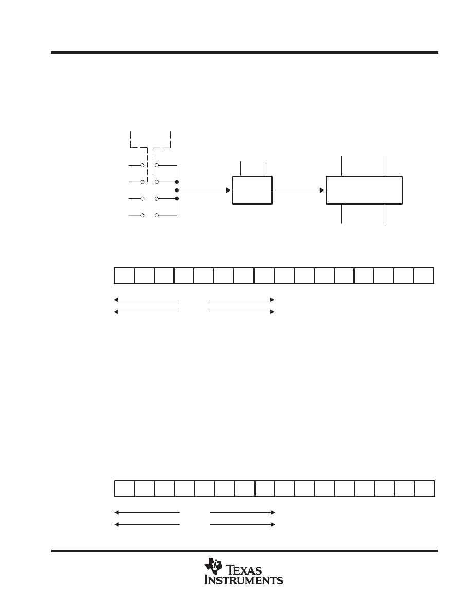
Two interrupt vectors are used by the Timer_A module. One individual vector is assigned to capture/compare
block CCR0, and one common interrupt vector is implemented for the timer and the other two capture/compare
blocks. The three interrupt events using the same vector are identified by an individual interrupt vector word.
The interrupt vector word is used to add an offset to the program counter to continue the interrupt handler
software at the corresponding program location. This simplifies the interrupt handler and gives each interrupt
event the same overhead of 5 cycles in the interrupt handler.
UART
Serial communication is implemented by using software and one capture/compare block. The hardware
supports the output of the serial-data stream, bit by bit, with the timing determined by the comparator/timer. The
data input uses the capture feature. The capture flag finds the start of a character, while the compare feature
latches the input-data stream, bit by bit. The software/hardware interface connects the mixed-signal controller
to external devices, systems, or networks.
MSP430F11x
MIXED SIGNAL MICROCONTROLLER
SLAS256B – NOVEMBER 1999 – REVISED JUNE 2000
21
POST OFFICE BOX 655303
•
DALLAS, TEXAS 75265
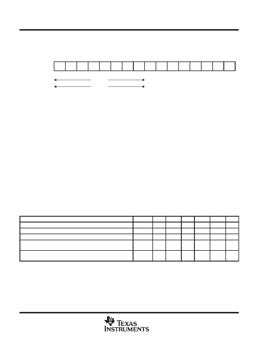
peripheral file map
PERIPHERALS WITH WORD ACCESS
Timer_A
Reserved
Reserved
Reserved
Reserved
Capture/compare register
Capture/compare register
Capture/compare register
Timer_A register
Reserved
Reserved
Reserved
Reserved
Capture/compare control
Capture/compare control
Capture/compare control
Timer_A control
Timer_A interrupt vector
CCR2
CCR1
CCR0
TAR
CCTL2
CCTL1
CCTL0
TACTL
TAIV
017Eh
017Ch
017Ah
0178h
0176h
0174h
0172h
0170h
016Eh
016Ch
016Ah
0168h
0166h
0164h
0162h
0160h
012Eh
Flash Memory
Flash control 3
Flash control 2
Flash control 1
FCTL3
FCTL2
FCTL1
012Ch
012Ah
0128h
Watchdog
Watchdog/timer control
WDTCTL
0120h
PERIPHERALS WITH BYTE ACCESS
System Clock
Basic clock sys. control2
Basic clock sys. control1
DCO clock freq. control
BCSCTL2
BCSCTL1
DCOCTL
058h
057h
056h
Port P2
Port P2 selection
Port P2 interrupt enable
Port P2 interrupt edge select
Port P2 interrupt flag
Port P2 direction
Port P2 output
Port P2 input
P2SEL
P2IE
P2IES
P2IFG
P2DIR
P2OUT
P2IN
02Eh
02Dh
02Ch
02Bh
02Ah
029h
028h
Port P1
Port P1 selection
Port P1 interrupt enable
Port P1 interrupt edge select
Port P1 interrupt flag
Port P1 direction
Port P1 output
Port P1 input
P1SEL
P1IE
P1IES
P1IFG
P1DIR
P1OUT
P1IN
026h
025h
024h
023h
022h
021h
020h
Special Function
SFR interrupt flag2
SFR interrupt flag1
SFR interrupt enable2
SFR interrupt enable1
IFG2
IFG1
IE2
IE1
003h
002h
001h
000h
MSP430F11x
MIXED SIGNAL MICROCONTROLLER
SLAS256B – NOVEMBER 1999 – REVISED JUNE 2000
22
POST OFFICE BOX 655303
•
DALLAS, TEXAS 75265
absolute maximum ratings
†
Voltage applied at V
CC
to V
SS
–0.3 V to 4.1 V
. . . . . . . . . . . . . . . . . . . . . . . . . . . . . . . . . . . . . . . . . . . . . . . . . . . . . .
Voltage applied to any pin (referenced to V
SS
)
–0.3 V to V
CC
+0.3 V
. . . . . . . . . . . . . . . . . . . . . . . . . . . . . . . . . . .
Diode current at any device terminal
±
2 mA
. . . . . . . . . . . . . . . . . . . . . . . . . . . . . . . . . . . . . . . . . . . . . . . . . . . . . . . .
Storage temperature, T
stg
(unprogrammed device)
–55
°
C to 150
°
C
. . . . . . . . . . . . . . . . . . . . . . . . . . . . . . . . . . .
Storage temperature, T
stg
(programmed device)
–40
°
C to 85
°
C
. . . . . . . . . . . . . . . . . . . . . . . . . . . . . . . . . . . . . .
† Stresses beyond those listed under “absolute maximum ratings” may cause permanent damage to the device. These are stress ratings only, and
functional operation of the device at these or any other conditions beyond those indicated under “recommended operating conditions” is not
implied. Exposure to absolute-maximum-rated conditions for extended periods may affect device reliability.
NOTE: All voltages referenced to VSS.
recommended operating conditions
MIN
NOM
MAX
UNITS
Supply voltage during program execution, VCC (see Note 6)
1.8
3.6
V
Supply voltage during program/erase flash memory, VCC
2.7
3.6
V
Supply voltage, VSS
0
V
Operating free-air temperature range, TA
–40
85
°
C
LFXT1
t l f
LF mode selected, XTS=0
Watch crystal
32 768
Hz
LFXT1 crystal frequency,
f(LFXT1) (see Note 7)
XT1 mode selected XTS=1
Ceramic resonator
450
8000
kHz
f(LFXT1) (see Note 7)
XT1 mode selected, XTS=1
Crystal
1000
8000
kHz
VCC = 1.8 V
dc
2
MHz
Processor frequency f(system) (MCLK signal)
VCC = 2.2 V
dc
5
MHz
( y
)
VCC = 3.6 V
dc
8
MHz
Flash timing generator frequency, f(FTG)
257
476
kHz
Cumulative program time, segment write, t(CPT) (see Note 8)
VCC = 2.7 V/3.6 V
3
ms
Low-level input voltage (TCK, TMS, TDI, RST/NMI), VIL
(excluding XIN, XOUT)
VCC = 2.2 V/3 V
VSS
VSS+0.6
V
High-level input voltage (TCK, TMS, TDI, RST/NMI), VIH
(excluding XIN, XOUT)
VCC = 2.2 V/3 V
0.8VCC
VCC
V
Input levels at XIN XOUT
VIL(XIN, XOUT)
VCC = 2 2 V/3 V
VSS
0.2
×
VCC
V
Input levels at XIN, XOUT
VIH(XIN, XOUT)
VCC = 2.2 V/3 V
0.8
×
VCC
VCC
V
NOTES:
6. The LFXT1 oscillator in LF-mode requires a resistor of 5.1 M
Ω
from XOUT to VSS when VCC <2.5 V.
The LFXT1 oscillator in XT1-mode accepts a ceramic resonator or a crystal frequency of 4 MHz at VCC
≥
2.2 V.
The LFXT1 oscillator in XT1-mode accepts a ceramic resonator or a crystal frequency of 8 MHz at VCC
≥
2.8 V.
7. The LFXT1 oscillator in LF-mode requires a watch crystal.
The LFXT1 oscillator in XT1-mode accepts a ceramic resonator or a crystal.
8. The cumulative program time must not be exceeded during a segment-write operation.
MSP430F11x
MIXED SIGNAL MICROCONTROLLER
SLAS256B – NOVEMBER 1999 – REVISED JUNE 2000
23
POST OFFICE BOX 655303
•
DALLAS, TEXAS 75265
recommended operating conditions (continued)
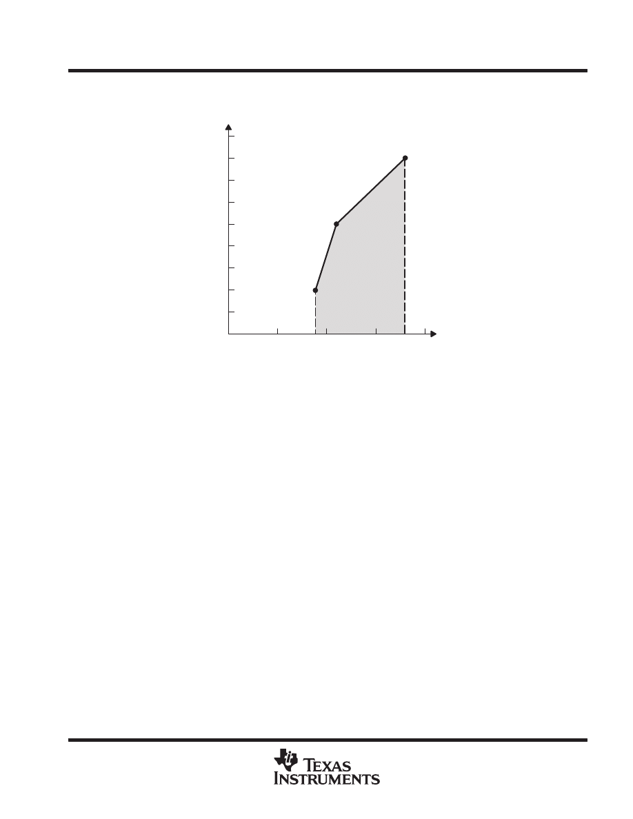
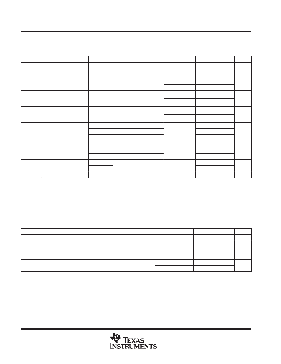
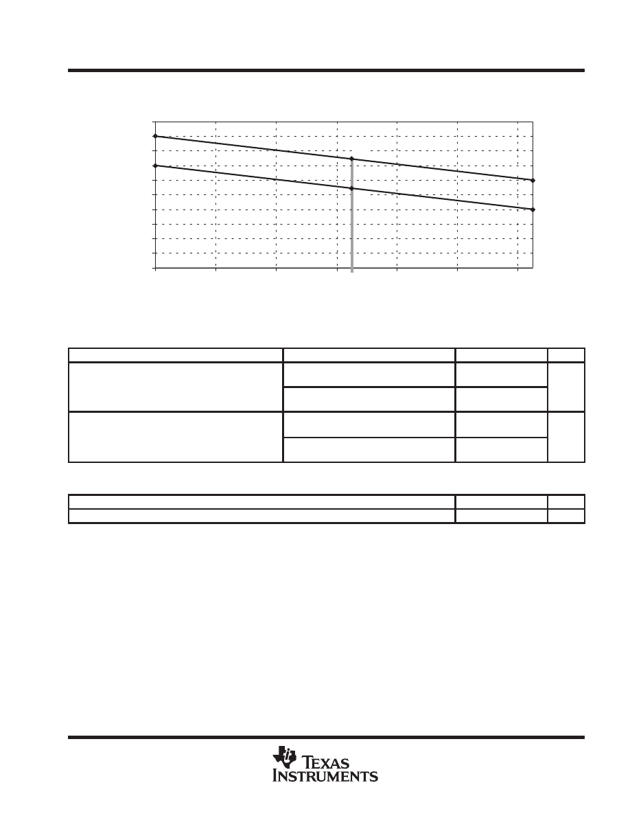
MSP430F11x Devices
NOTE: Minimum processor frequency is defined by system clock. Flash
program or erase operations require a minimum VCC of 2.7 V.
9
3
2
1
0
0
1
2
3
4
4
5 MHz at
2.2 V
VCC – Supply Voltage – V
8 MHz at
3.6 V
f (system)
– Maximum Processor
Frequency – MHz
5
6
7
8
2 MHz at
1.8 V
Figure 5. Frequency vs Supply Voltage
MSP430F11x
MIXED SIGNAL MICROCONTROLLER
SLAS256B – NOVEMBER 1999 – REVISED JUNE 2000
24
POST OFFICE BOX 655303
•
DALLAS, TEXAS 75265
electrical characteristics over recommended ranges of supply voltage and operating free-air
temperature (unless otherwise noted)
supply current (into V
CC
) excluding external current (f
(system)
= 1 MHz)
PARAMETER
TEST CONDITIONS
MIN
TYP
MAX
UNIT
TA = –40
°
C +85
°
C,
f(MCLK) = f(SMCLK) = 1 MHz
VCC = 2.2 V
200
250
µ
A
I(AM)
Active mode
f(MCLK) = f(SMCLK) = 1 MHz,
f(ACLK) = 32,768 Hz
VCC = 3 V
300
350
µ
A
I(AM)
Active mode
TA = –40
°
C +85
°
C,
VCC = 2.2 V
1.6
3
µ
A
A
f(MCLK) = f(SMCLK) = f(ACLK) = 4096 Hz
VCC = 3 V
3
4.3
µ
A
I(CPUOff)
Low power mode (LPM0)
TA = –40
°
C +85
°
C,
f(MCLK) = 0 f(SMCLK) = 1 MHz
VCC = 2.2 V
32
45
µ
A
I(CPUOff)
Low-power mode, (LPM0)
f(MCLK) = 0, f(SMCLK) = 1 MHz,
f(ACLK) = 32,768 Hz
VCC = 3 V
55
70
µ
A
I(LPM2)
Low power mode (LPM2)
TA = –40
°
C +85
°
C,
f(MCLK) = f(SMCLK) = 0 MHz
VCC = 2.2 V
11
14
µ
A
I(LPM2)
Low-power mode, (LPM2)
f(MCLK) = f(SMCLK) = 0 MHz,
f(ACLK) = 32,768 Hz, SCG0 = 0
VCC = 3 V
17
22
µ
A
TA = –40
°
C
0.8
1.2
TA = 25
°
C
VCC = 2.2 V
0.7
1
µ
A
I(LPM3)
Low power mode (LPM3)
TA = 85
°
C
1.6
2.3
I(LPM3)
Low-power mode, (LPM3)
TA = –40
°
C
1.8
2.2
TA = 25
°
C
VCC = 3 V
1.6
1.9
µ
A
TA = 85
°
C
2.3
3.4
TA = –40
°
C
f(MCLK) = 0 MHz
0.1
0.5
I(LPM4)
Low-power mode, (LPM4)
TA = 25
°
C
f(MCLK) 0 MHz
f(SMCLK) = 0 MHz,
0 H
SCG0
1
VCC = 2.2 V/3 V
0.1
0.5
µ
A
(
)
TA = 85
°
C
(
)
f(ACLK) = 0 Hz, SCG0 = 1
0.8
1.9
NOTE: All inputs are tied to 0 V or VCC. Outputs do not source or sink any current.
current consumption of active mode versus system frequency, F version
I
AM
= I
AM[1 MHz]
×
f
system
[MHz]
current consumption of active mode versus supply voltage, F version
I
AM
= I
AM[3 V]
+ 120
µ
A/V
×
(V
CC
–3 V)
Schmitt-trigger inputs Port 1 to Port P2; P1.0 to P1.7, P2.0 to P2.5
PARAMETER
TEST CONDITIONS
MIN
TYP
MAX
UNIT
VIT
Positive going input threshold voltage
VCC = 2.2 V
1.1
1.3
V
VIT+
Positive-going input threshold voltage
VCC = 3 V
1.5
1.8
V
VIT
Negative going input threshold voltage
VCC = 2.2 V
0.4
0.9
V
VIT–
Negative-going input threshold voltage
VCC = 3 V
.90
1.2
V
Vh
Input voltage hysteresis (VIT
VIT )
VCC = 2.2 V
0.3
1
V
Vhys
Input voltage hysteresis, (VIT+ – VIT–)
VCC = 3 V
0.5
1.4
V
MSP430F11x
MIXED SIGNAL MICROCONTROLLER
SLAS256B – NOVEMBER 1999 – REVISED JUNE 2000
25
POST OFFICE BOX 655303
•
DALLAS, TEXAS 75265
electrical characteristics over recommended ranges of supply voltage and operating free-air
temperature (unless otherwise noted)
outputs Port 1 to P2; P1.0 to P1.7, P2.0 to P2.5
PARAMETER
TEST CONDITIONS
MIN
TYP
MAX
UNIT
I(OHmax) = –1.5 mA
VCC = 2 2 V
See Note 9
VCC–0.25
VCC
VOH
High-level output voltage
I(OHmax) = –6 mA
VCC = 2.2 V
See Note 10
VCC–0.6
VCC
V
VOH
g
g
Port 1
I(OHmax) = –1.5 mA
VCC = 3 V
See Note 9
VCC–0.25
VCC
V
I(OHmax) = –6 mA
VCC = 3 V
See Note 10
VCC–0.6
VCC
I(OHmax) = –1 mA
VCC = 2 2 V
See Note 11
VCC–0.25
VCC
VOH
High-level output voltage
I(OHmax) = –3.4 mA
VCC = 2.2 V
See Note 11
VCC–0.6
VCC
V
VOH
g
g
Port 2
I(OHmax) = –1 mA
VCC = 3 V
See Note 11
VCC–0.25
VCC
V
I(OHmax) = –3.4 mA
VCC = 3 V
See Note 11
VCC–0.6
VCC
I(OLmax) = 1.5 mA
VCC = 2 2 V
See Note 9
VSS
VSS+0.25
VOL
Low-level output voltage
I(OLmax) = 6 mA
VCC = 2.2 V
See Note 10
VSS
VSS+0.6
V
VOL
g
Port 1 and Port 2
I(OLmax) = 1.5 mA
VCC = 3 V
See Note 9
VSS
VSS+0.25
V
I(OLmax) = 6 mA
VCC = 3 V
See Note 10
VSS
VSS+0.6
NOTES:
9. The maximum total current, IOHmax and IOLmax, for all outputs combined, should not exceed
±
12 mA to hold the maximum voltage
drop specified.
10. The maximum total current, IOHmax and IOLmax, for all outputs combined, should not exceed
±
48 mA to hold the maximum voltage
drop specified.
11. One output loaded at a time.
leakage current
PARAMETER
TEST CONDITIONS
MIN
TYP
MAX
UNIT
Ilk (P
)
High impedance leakage current
Port P1: P1.x, 0
≤
× ≤
7
(see Notes 12 and 13)
VCC = 2.2 V/3 V,
±
50
nA
Ilkg(Px.x)
High-impedance leakage current
Port P2: P2.x, 0
≤
× ≤
5
(see Notes 12 and 13)
VCC = 2.2 V/3 V,
±
50
nA
NOTES: 12. The leakage current is measured with VSS or VCC applied to the corresponding pin(s), unless otherwise noted.
13. The leakage of the digital port pins is measured individually. The port pin must be selected for input and there must be no optional
pullup or pulldown resistor.
inputs Px.x, TAx
PARAMETER
TEST CONDITIONS
VCC
MIN
TYP
MAX
UNIT
Port P1, P2: P1.x to P2.x,
2.2 V/3 V
1.5
cycle
t(int)
External interrupt timing
Port P1, P2: P1.x to P2.x,
External trigger signal for the interrupt flag,
2.2 V
62
ns
(
)
(see Note 14)
3 V
50
ns
2.2 V/3 V
1.5
cycle
t(cap)
Timer_A, capture timing
TA0, TA1, TA2. (see Note 15)
2.2 V
62
ns
(
)
3 V
50
ns
NOTES: 14. The external signal sets the interrupt flag every time the minimum tint cycle and time parameters are met. It may be set even with
trigger signals shorter than tint. Both the cycle and timing specifications must be met to ensure the flag is set. tint is measured in MCLK
cycles.
15. The external capture signal triggers the capture event every time when the minimum tcap cycles and time parameters are met. A
capture may be triggered with capture signals even shorter than tcap. Both the cycle and timing specifications must be met to ensure
a correct capture of the 16-bit timer value and to ensure the flag is set.
MSP430F11x
MIXED SIGNAL MICROCONTROLLER
SLAS256B – NOVEMBER 1999 – REVISED JUNE 2000
26
POST OFFICE BOX 655303
•
DALLAS, TEXAS 75265
electrical characteristics over recommended ranges of supply voltage and operating free-air
temperature (unless otherwise noted) (continued)
internal signals TAx, SMCLK at Timer_A
PARAMETER
TEST CONDITIONS
VCC
MIN
TYP
MAX
UNIT
f(IN)
Input frequency
Internal TA0 TA1 TA2 tH = tL
2.2 V
8
MHz
f(IN)
Input frequency
Internal TA0, TA1, TA2, tH = tL
3 V
10
MHz
f(TAint)
Timer_A clock frequency
Internally, SMCLK signal applied
2.2 V/3 V
dc
fSystem
outputs P1.x, P2.x, TAx
PARAMETER
TEST CONDITIONS
VCC
MIN
TYP
MAX
UNIT
f(P20)
P2.0/ACLK,
CL = 20 pF
2.2 V/3 V
fSystem
f(TAx)
Output frequency
TA0, TA1, TA2,
CL = 20 pF
Internal clock source, SMCLK signal applied
(See Note 16)
2.2 V/3 V
dc
fSystem
MHz
fSMCLK = fLFXT1 = fXT1
40%
60%
fSMCLK = fLFXT1 = fLF
2 2 V/3 V
35%
65%
P1.4/SMCLK, CL = 20 pF
fSMCLK = fLFXT1/n
2.2 V/3 V
50%–
15 ns
50%
50%+
15 ns
t(Xdc)
Duty cycle of O/P
frequency
fSMCLK = fDCOCLK
2.2 V/3 V
50%–
15 ns
50%
50%+
15 ns
fP20 = fLFXT1 = fXT1
40%
60%
P2.0/ACLK, CL = 20 pF
fP20 = fLFXT1 = fLF
2.2 V/3 V
30%
70%
fP20 = fLFXT1/n
50%
t(TAdc)
TA0, TA1, TA2, CL = 20 pF, Duty cycle = 50%
2.2 V/3 V
0
±
50
ns
NOTE 16: The limits of the system clock MCLK have to be met. MCLK and SMCLK can have different frequencies.
PUC/POR
PARAMETER
TEST CONDITIONS
MIN
TYP
MAX
UNIT
t(POR_delay)
150
250
µ
s
TA = –40
°
C
1.4
1.8
V
V(POR)
POR
TA = 25
°
C
VCC = 2 2 V/3 V
1.1
1.5
V
(
)
TA = 85
°
C
VCC = 2.2 V/3 V
0.8
1.2
V
V(min)
0
0.4
V
t(reset)
PUC/POR
Reset is accepted internally
2
µ
s
VCC
POR
V
t
V
(POR)
V
(min)
POR
No POR
Figure 6. Power-On Reset (POR) vs Supply Voltage
MSP430F11x
MIXED SIGNAL MICROCONTROLLER
SLAS256B – NOVEMBER 1999 – REVISED JUNE 2000
27
POST OFFICE BOX 655303
•
DALLAS, TEXAS 75265
electrical characteristics over recommended ranges of supply voltage and operating free-air
temperature (unless otherwise noted) (continued)
0
0.2
0.6
1.0
1.2
1.8
2.0
–40
–20
0
20
40
60
80
Temperature [
°
C]
V POR [V]
1.6
1.4
0.8
0.4
1.2
1.5
1.8
0.8
1.1
1.4
25
°
C
Max
Min
Figure 7. V
(POR)
vs Temperature
crystal oscillator,LFXT1
PARAMETER
TEST CONDITIONS
MIN
TYP
MAX
UNIT
C(XIN)
Input capacitance
XTS=0; LF mode selected.
VCC = 2.2 V / 3 V
12
pF
C(XIN)
Input capacitance
XTS=1; XT1 mode selected.
VCC = 2.2 V / 3 V (Note 17)
2
pF
C(XOUT)
Output capacitance
XTS=0; LF mode selected.
VCC = 2.2 V / 3 V
12
pF
C(XOUT)
Out ut ca acitance
XTS=1; XT1 mode selected.
VCC = 2.2 V / 3 V (Note 17)
2
F
NOTE 17: Requires external capacitors at both terminals. Values are specified by crystal manufacturers.
RAM
PARAMETER
MIN
TYP
MAX
UNIT
V(RAMh)
CPU halted (see Note 18)
1.6
V
NOTE 18: This parameter defines the minimum supply voltage VCC when the data in the program memory RAM remains unchanged. No program
execution should happen during this supply voltage condition.
MSP430F11x
MIXED SIGNAL MICROCONTROLLER
SLAS256B – NOVEMBER 1999 – REVISED JUNE 2000
28
POST OFFICE BOX 655303
•
DALLAS, TEXAS 75265
electrical characteristics over recommended ranges of supply voltage and operating free-air
temperature (unless otherwise noted) (continued)
DCO
PARAMETER
TEST CONDITIONS
MIN
TYP
MAX
UNIT
f(DCO03)
R
l = 0 DCO = 3 MOD = 0 DCOR = 0
TA = 25
°
C
VCC = 2.2 V
0.08
0.12
0.15
MHz
f(DCO03)
Rsel = 0, DCO = 3, MOD = 0, DCOR = 0, TA = 25
°
C
VCC = 3 V
0.08
0.13
0.16
MHz
f(DCO13)
R
l = 1 DCO = 3 MOD = 0 DCOR = 0
TA = 25
°
C
VCC = 2.2 V
0.14
0.19
0.23
MHz
f(DCO13)
Rsel = 1, DCO = 3, MOD = 0, DCOR = 0, TA = 25
°
C
VCC = 3 V
0.14
0.18
0.22
MHz
f(DCO23)
R
l = 2 DCO = 3 MOD = 0 DCOR = 0
TA = 25
°
C
VCC = 2.2 V
0.22
0.30
0.36
MHz
f(DCO23)
Rsel = 2, DCO = 3, MOD = 0, DCOR = 0, TA = 25
°
C
VCC = 3 V
0.22
0.28
0.34
MHz
f(DCO33)
R
l = 3 DCO = 3 MOD = 0 DCOR = 0
TA = 25
°
C
VCC = 2.2 V
0.37
0.49
0.59
MHz
f(DCO33)
Rsel = 3, DCO = 3, MOD = 0, DCOR = 0, TA = 25
°
C
VCC = 3 V
0.37
0.47
0.56
MHz
f(DCO43)
R
l = 4 DCO = 3 MOD = 0 DCOR = 0
TA = 25
°
C
VCC = 2.2 V
0.61
0.77
0.93
MHz
f(DCO43)
Rsel = 4, DCO = 3, MOD = 0, DCOR = 0, TA = 25
°
C
VCC = 3 V
0.61
0.75
0.9
MHz
f(DCO53)
R
l = 5 DCO = 3 MOD = 0 DCOR = 0
TA = 25
°
C
VCC = 2.2 V
1
1.2
1.5
MHz
f(DCO53)
Rsel = 5, DCO = 3, MOD = 0, DCOR = 0, TA = 25
°
C
VCC = 3 V
1
1.3
1.5
MHz
f(DCO63)
R
l = 6 DCO = 3 MOD = 0 DCOR = 0
TA = 25
°
C
VCC = 2.2 V
1.6
1.9
2.2
MHz
f(DCO63)
Rsel = 6, DCO = 3, MOD = 0, DCOR = 0, TA = 25
°
C
VCC = 3 V
1.69
2.0
2.29
MHz
f(DCO73)
R
l = 7 DCO = 3 MOD = 0 DCOR = 0
TA = 25
°
C
VCC = 2.2 V
2.4
2.9
3.4
MHz
f(DCO73)
Rsel = 7, DCO = 3, MOD = 0, DCOR = 0, TA = 25
°
C
VCC = 3 V
2.7
3.2
3.65
MHz
f(DCO77)
Rsel = 7 DCO = 7 MOD = 0 DCOR = 0
TA = 25
°
C
VCC = 2.2 V
4
4.5
4.9
MHz
f(DCO77)
Rsel = 7, DCO = 7, MOD = 0, DCOR = 0, TA = 25
°
C
VCC = 3 V
4.4
4.9
5.4
MHz
f(DCO47)
R
l = 4 DCO = 7 MOD = 0 DCOR = 0
TA = 25
°
C
VCC = 2 2 V/3 V
FDCO40 FDCO40 FDCO40
MHz
f(DCO47)
Rsel = 4, DCO = 7, MOD = 0, DCOR = 0, TA = 25
°
C
VCC = 2.2 V/3 V
DCO40
x1.7
DCO40
x2.1
DCO40
x2.5
MHz
S(Rsel)
SR = fRsel+1/fRsel
VCC = 2.2 V/3 V
1.35
1.65
2
ratio
S(DCO)
SDCO = fDCO+1/fDCO
VCC = 2.2 V/3 V
1.07
1.12
1.16
ratio
Dt
Temperature drift, Rsel = 4, DCO = 3, MOD = 0
VCC = 2.2 V
–0.31
–0.36
–0.40
%/
°
C
Dt
sel
(see Note 18)
VCC = 3 V
–0.33
–0.38
–0.43
%/
°
C
DV
Drift with VCC variation, Rsel = 4, DCO = 3, MOD = 0
(see Note 19)
VCC = 2.2 V/3 V
0
5
10
%/V
NOTE 19: These parameters are not production tested.
ÎÎÎÎÎÎ
ÎÎÎÎÎÎ
ÎÎÎÎÎÎ
ÎÎÎÎÎÎ
2.2 V
3 V
VCC
Max
Min
Max
Min
f(DCOx7)
f(DCOx0)
Frequency V
ariance
0
1
2
3
4
5
6
7
DCO Steps
1
f DCOCLK
Figure 8. DCO Characteristics
MSP430F11x
MIXED SIGNAL MICROCONTROLLER
SLAS256B – NOVEMBER 1999 – REVISED JUNE 2000
29
POST OFFICE BOX 655303
•
DALLAS, TEXAS 75265
electrical characteristics over recommended ranges of supply voltage and operating free-air
temperature (unless otherwise noted) (continued)
principle characteristics of the DCO
D
Individual devices have a minimum and maximum operation frequency. The specified parameters for
f
DCOx0
to f
DCOx7
are valid for all devices.
D
The DCO control bits DCO0, DCO1 and DCO2 have a step size as defined in parameter S
DCO
.
D
The modulation control bits MOD0 to MOD4 select how often f
DCO+1
is used within the period of 32 DCOCLK
cycles. f
DCO
is used for the remaining cycles. The frequency is an average = f
DCO
×
(2
MOD/32
).
D
The ranges selected by R
Sel4
to R
Sel5
, R
Sel5
to R
Sel6
, and R
Sel6
to R
Sel7
are overlapping.
wake-up from lower power modes (LPMx)
PARAMETER
TEST CONDITIONS
MIN
TYP
MAX
UNIT
t(LPM0)
VCC = 2.2 V/3 V
100
ns
t(LPM2)
VCC = 2.2 V/3 V
100
ns
f(MCLK) = 1 MHz,
VCC = 2.2 V/3 V
6
t(LPM3)
Delay time (see Note 20)
f(MCLK) = 2 MHz,
VCC = 2.2 V/3 V
6
µ
s
(
)
Delay time (see Note 20)
f(MCLK) = 3 MHz,
VCC = 2.2 V/3 V
6
f(MCLK) = 1 MHz,
VCC = 2.2 V/3 V
6
t(LPM4)
f(MCLK) = 2 MHz,
VCC = 2.2 V/3 V
6
µ
s
(
)
f(MCLK) = 3 MHz,
VCC = 2.2 V/3 V
6
NOTE 20: Parameter applicable only if DCOCLK is used for MCLK.
JTAG/programming
PARAMETER
TEST CONDITIONS
MIN
TYP
MAX
UNIT
f(TCK)
TCK frequency JTAG/test (see Note 21)
VCC = 2.2 V
dc
5
MHz
f(TCK)
TCK frequency, JTAG/test (see Note 21)
VCC = 3 V
dc
10
MHz
I(DD-PGM)
Current during program cycle (see Note 22)
VCC = 2.7 V/3.6 V
3
5
mA
I(DD-ERASE)
Current during erase cycle (see Note 22)
VCC = 2.7 V/3.6 V
3
5
mA
t( t ti )
Write/erase cycles
10
4
10
5
t(retention)
Data retention TA = 25
°
C
100
Year
NOTES: 21. f(TCK) may be restricted to meet the timing requirements of the module selected.
22. Duration of the program/erase cycle is determined by f(FTG) applied to the flash timing controller. It can be calculated as follows:
t(word write) = 35 x 1/f(FTG)
t(segment write, byte 0) = 30
×
1/f(FTG)
t(segment write, byte 1 – 63) = 20
×
1/f(FTG)
t(mass erase) = 5297 x 1/f(FTG)
t(page erase) = 4819 x 1/f(FTG)
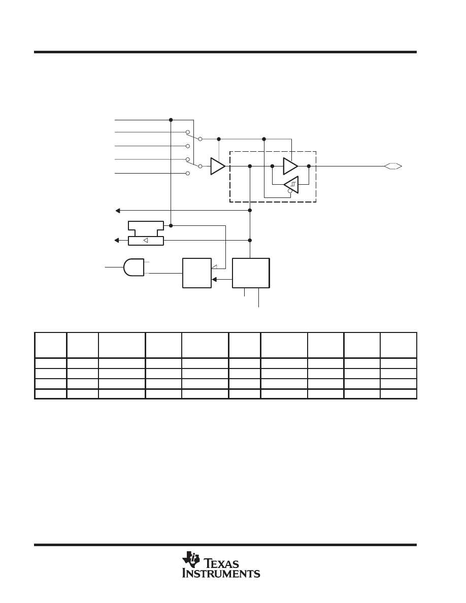
MSP430F11x
MIXED SIGNAL MICROCONTROLLER
SLAS256B – NOVEMBER 1999 – REVISED JUNE 2000
30
POST OFFICE BOX 655303
•
DALLAS, TEXAS 75265
APPLICATION INFORMATION
input/output schematic
Port P1, P1.0 to P1.3, input/output with Schmitt-trigger
EN
D
P1.0 – P1.3
0
1
0
1
Interrupt
Edge
Select
EN
Set
Q
P1IE.x
P1IFG.x
P1IRQ.x
Interrupt
Flag
P1IES.x
P1SEL.x
Module X IN
P1IN.x
P1OUT.x
Module X OUT
Direction Control
From Module
P1DIR.x
P1SEL.x
Pad Logic
NOTE: x = Bit/identifier, 0 to 3 for port P1
PnSel.x
PnDIR.x
Direction
control from
module
PnOUT.x
Module X OUT
PnIN.x
Module X IN
PnIE.x
PnIFG.x
PnIES.x
P1Sel.0
P1DIR.0
P1DIR.0
P1OUT.0
VSS
P1IN.0
TACLK†
P1IE.0
P1IFG.0
P1IES.0
P1Sel.1
P1DIR.1
P1DIR.1
P1OUT.1
Out0 signal†
P1IN.1
CCI0A†
P1IE.1
P1IFG.1
P1IES.1
P1Sel.2
P1DIR.2
P1DIR.2
P1OUT.2
Out1 signal†
P1IN.2
CCI1A†
P1IE.2
P1IFG.2
P1IES.2
P1Sel.3
P1DIR.3
P1DIR.3
P1OUT.3
Out2 signal†
P1IN.3
CCI2A†
P1IE.3
P1IFG.3
P1IES.3
† Signal from or to Timer_A
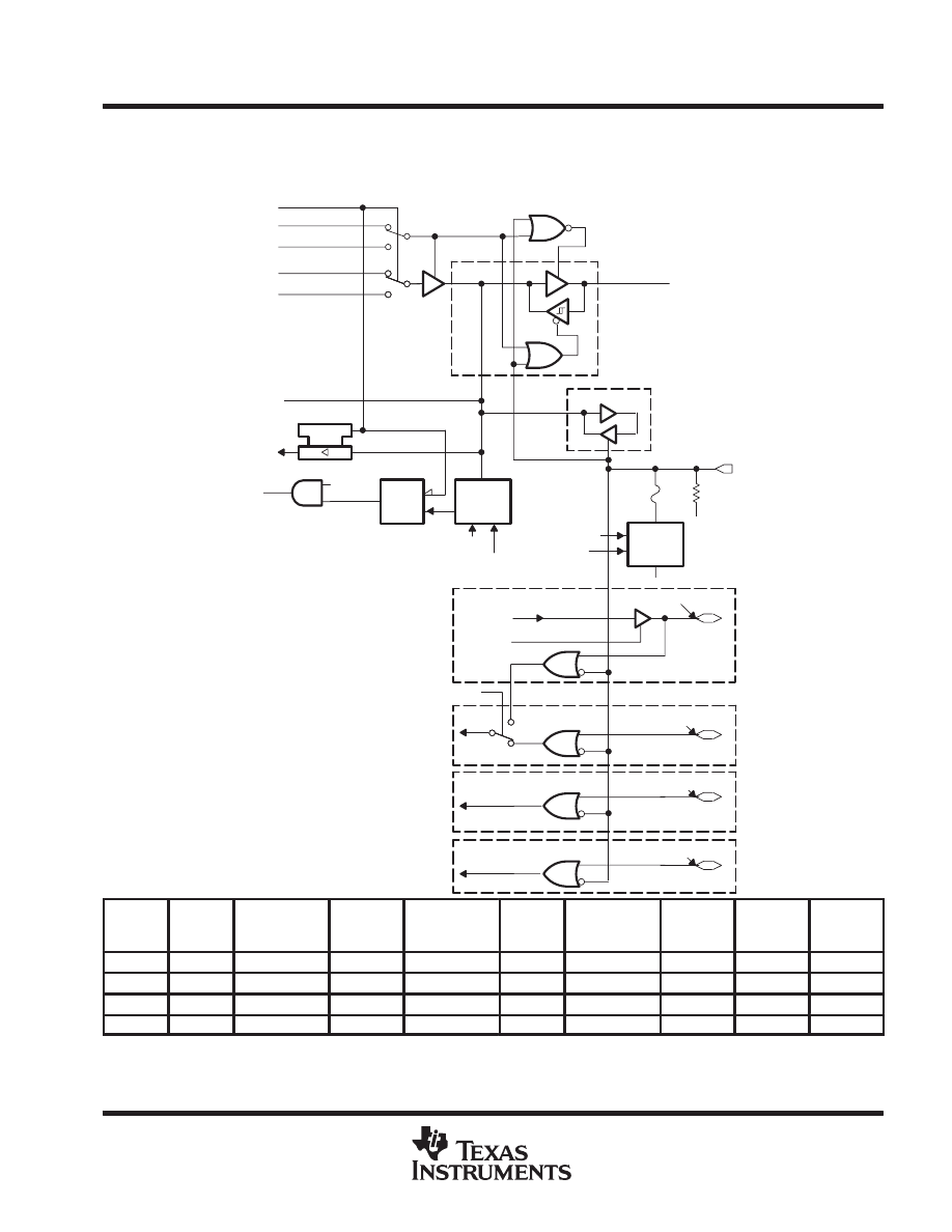
MSP430F11x
MIXED SIGNAL MICROCONTROLLER
SLAS256B – NOVEMBER 1999 – REVISED JUNE 2000
31
POST OFFICE BOX 655303
•
DALLAS, TEXAS 75265
APPLICATION INFORMATION
Port P1, P1.4 to P1.7, input/output with Schmitt-trigger and in-system access features
EN
D
P1.4–P1.7
0
1
0
1
Interrupt
Edge
Select
EN
Set
Q
P1IE.x
P1IFG.x
P1IRQ.x
Interrupt
Flag
P1IES.x
P1SEL.x
Module X IN
P1IN.x
P1OUT.x
Module X OUT
Direction Control
From Module
P1DIR.x
P1SEL.x
Pad Logic
Bus Keeper
TST
Fuse
60 k
Ω
Fuse
Blow
Control
Control By JTAG
0
1
TDO
Controlled By JTAG
P1.x
TDI
P1.x
TST
TST
TMS
TST
TCK
TST
Controlled by JTAG
TST
P1.x
P1.x
NOTE: The test pin should be protected from potential EMI
and ESD voltage spikes. This may require a smaller
external pulldown resistor in some applications.
x = Bit identifier, 4 to 7 for port P1
During programming activity and during blowing
the fuse, the pin TDO/TDI is used to apply the test
input for JTAG circuitry.
P1.7/TDI/TDO
P1.6/TDI
P1.5/TMS
P1.4/TCK
Typical
TEST
GND
NOTE: Fuse not implemented
in F11x
PnSel.x
PnDIR.x
Direction
control from
module
PnOUT.x
Module X OUT
PnIN.x
Module X IN
PnIE.x
PnIFG.x
PnIES.x
P1Sel.4
P1DIR.4
P1DIR.4
P1OUT.4
SMCLK
P1IN.4
unused
P1IE.4
P1IFG.4
P1IES.4
P1Sel.5
P1DIR.5
P1DIR.5
P1OUT.5
Out0 signal†
P1IN.5
unused
P1IE.5
P1IFG.5
P1IES.5
P1Sel.6
P1DIR.6
P1DIR.6
P1OUT.6
Out1 signal†
P1IN.6
unused
P1IE.6
P1IFG.6
P1IES.6
P1Sel.7
P1DIR.7
P1DIR.7
P1OUT.7
Out2 signal†
P1IN.7
unused
P1IE.7
P1IFG.7
P1IES.7
† Signal from or to Timer_A
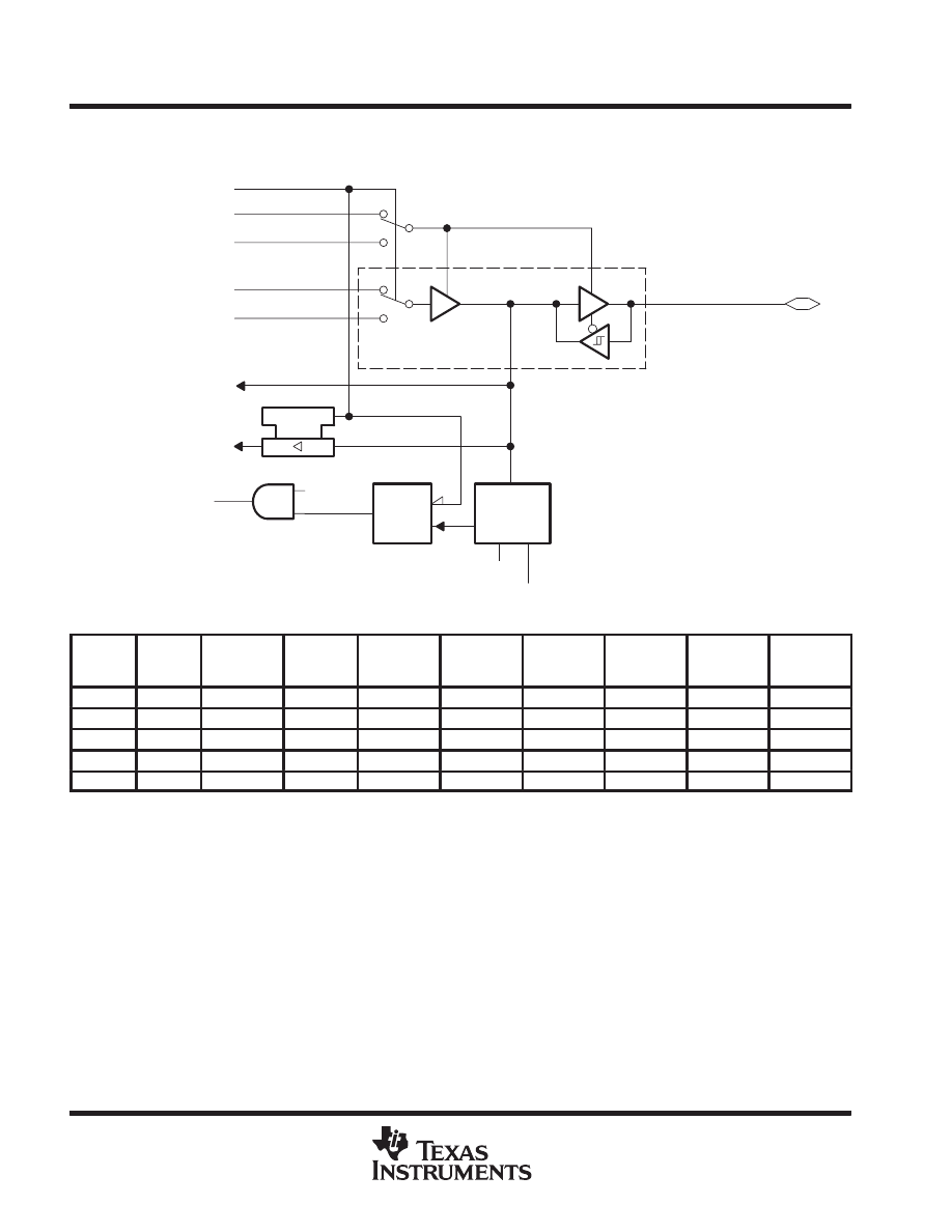
MSP430F11x
MIXED SIGNAL MICROCONTROLLER
SLAS256B – NOVEMBER 1999 – REVISED JUNE 2000
32
POST OFFICE BOX 655303
•
DALLAS, TEXAS 75265
APPLICATION INFORMATION
Port P2, P2.0 to P2.4, input/output with Schmitt-trigger
EN
D
P2.0 – P2.4
0
1
0
1
Interrupt
Edge
Select
EN
Set
Q
P2IE.x
P2IFG.x
P2IRQ.x
Interrupt
Flag
P2IES.x
P2SEL.x
Module X IN
P2IN.x
P2OUT.x
Module X OUT
Direction Control
From Module
P2DIR.x
P2SEL.x
Pad Logic
NOTE: x = Bit Identifier, 0 to 4 For Port P2
0: Input
1: Output
PnSel.x
PnDIR.x
Direction
control from
module
PnOUT.x
Module X
OUT
PnIN.x
Module X
IN
PnIE.x
PnIFG.x
PnIES.x
P2Sel.0
P2DIR.0
P2DIR.0
P2OUT.0
ACLK
P2IN.0
unused
P2IE.0
P2IFG.0
P1IES.0
P2Sel.1
P2DIR.1
P2DIR.1
P2OUT.1
VSS
P2IN.1
INCLK†
P2IE.1
P2IFG.1
P1IES.1
P2Sel.2
P2DIR.2
P2DIR.2
P2OUT.2
Out0 signal†
P2IN.2
CCI0B†
P2IE.2
P2IFG.2
P1IES.2
P2Sel.3
P2DIR.3
P2DIR.3
P2OUT.3
Out1 signal†
P2IN.3
CCI1B†
P2IE.3
P2IFG.3
P1IES.3
P2Sel.4
P2DIR.4
P2DIR.4
P2OUT.4
Out2 signal†
P2IN.4
unused
P2IE.4
P2IFG.4
P1IES.4
† Signal from or to Timer_A
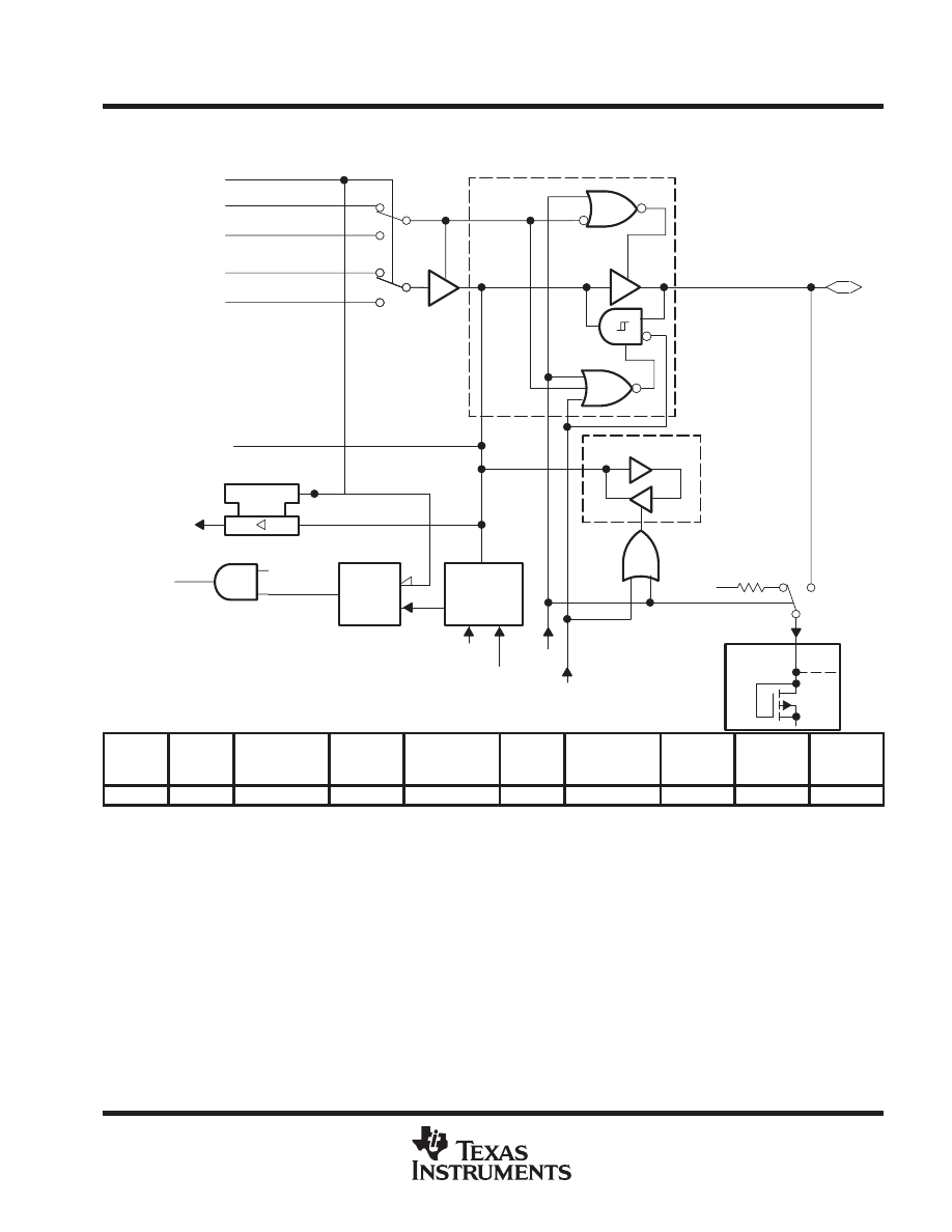
MSP430F11x
MIXED SIGNAL MICROCONTROLLER
SLAS256B – NOVEMBER 1999 – REVISED JUNE 2000
33
POST OFFICE BOX 655303
•
DALLAS, TEXAS 75265
Port P2, P2.5, input/output with Schmitt-trigger and R
OSC
function for the Basic Clock module
EN
D
P2.5
0
1
0
1
Interrupt
Edge
Select
EN
Set
Q
P2IE.5
P2IFG.5
P2IRQ.5
Interrupt
Flag
P2IES.5
P2SEL.5
Module X IN
P2IN.5
P2OUT.5
Module X OUT
Direction Control
From Module
P2DIR.5
P2SEL.5
Pad Logic
NOTE: DCOR: Control bit from basic clock module if it is set, P2.5 Is disconnected from P2.5 pad
Bus Keeper
0
1
0
1
VCC
Internal to
Basic Clock
Module
DCOR
DC
Generator
0: Input
1: Output
CAPD.5
PnSel.x
PnDIR.x
Direction
control from
module
PnOUT.x
Module X OUT
PnIN.x
Module X IN
PnIE.x
PnIFG.x
PnIES.x
P2Sel.5
P2DIR.5
P2DIR.5
P2OUT.5
VSS
P2IN.5
unused
P2IE.5
P2IFG.5
P2IES.5
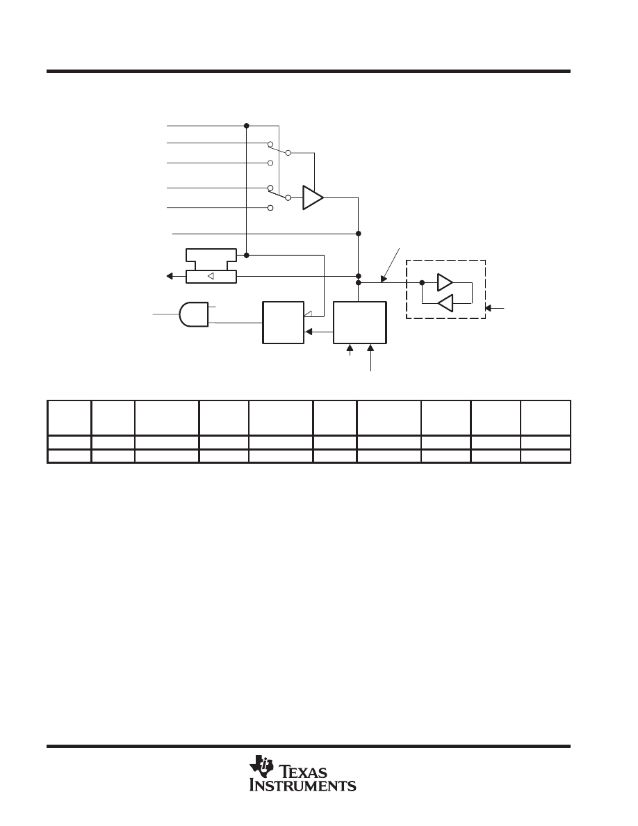
MSP430F11x
MIXED SIGNAL MICROCONTROLLER
SLAS256B – NOVEMBER 1999 – REVISED JUNE 2000
34
POST OFFICE BOX 655303
•
DALLAS, TEXAS 75265
APPLICATION INFORMATION
Port P2, unbonded bits P2.6 and P2.7
EN
D
0
1
0
1
Interrupt
Edge
Select
EN
Set
Q
P2IE.x
P2IFG.x
P2IRQ.x
Interrupt
Flag
P2IES.x
P2SEL.x
Module X IN
P2IN.x
P2OUT.x
Module X OUT
Direction Control
From Module
P2DIR.x
P2SEL.x
Bus Keeper
0
1
0: Input
1: Output
Node Is Reset With PUC
PUC
NOTE: x = Bit/identifier, 6 to 7 for port P2 without external pins
P2Sel.x
P2DIR.x
Direction
control from
module
P2OUT.x
Module X OUT
P2IN.x
Module X IN
P2IE.x
P2IFG.x
P2IES.x
P2Sel.6
P2DIR.6
P2DIR.6
P2OUT.6
VSS
P2IN.6
unused
P2IE.6
P2IFG.6
P2IES.6
P2Sel.7
P2DIR.7
P2DIR.7
P2OUT.7
VSS
P2IN.7
unused
P2IE.7
P2IFG.7
P2IES.7
NOTE: A good use of the unbonded bits 6 and 7 of port P2 is to use the interrupt flags. The interrupt flags can not be influenced from any signal
other than from software. They work then as a soft interrupt.
JTAG fuse check mode
MSP430 devices that have the fuse on the TEST terminal have a fuse check mode that tests the continuity of
the fuse the first time the JTAG port is accessed after a power-on reset (POR). When activated, a fuse check
current can flow from the TEST pin to ground if the fuse is not burned. Care must be taken to avoid accidentally
activating the fuse check mode and increasing overall system power consumption.
When the TEST pin is taken back low after a test or programming session, the fuse check mode and sense
currents are terminated.
MSP430F11x
MIXED SIGNAL MICROCONTROLLER
SLAS256B – NOVEMBER 1999 – REVISED JUNE 2000
35
POST OFFICE BOX 655303
•
DALLAS, TEXAS 75265
MECHANICAL DATA
DW (R-PDSO-G**)
PLASTIC SMALL-OUTLINE PACKAGE
16 PIN SHOWN
4040000 / D 02/98
Seating Plane
0.400 (10,15)
0.419 (10,65)
0.104 (2,65) MAX
1
0.012 (0,30)
0.004 (0,10)
A
8
16
0.020 (0,51)
0.014 (0,35)
0.293 (7,45)
0.299 (7,59)
9
0.010 (0,25)
0.050 (1,27)
0.016 (0,40)
(15,24)
(15,49)
PINS **
0.010 (0,25) NOM
A MAX
DIM
A MIN
Gage Plane
20
0.500
(12,70)
(12,95)
0.510
(10,16)
(10,41)
0.400
0.410
16
0.600
24
0.610
0.004 (0,10)
M
0.010 (0,25)
0.050 (1,27)
0
°
– 8
°
NOTES: A. All linear dimensions are in inches (millimeters).
B. This drawing is subject to change without notice.
C. Body dimensions do not include mold flash or protrusion not to exceed 0.006 (0,15).
D. Falls within JEDEC MS-013
MSP430F11x
MIXED SIGNAL MICROCONTROLLER
SLAS256B – NOVEMBER 1999 – REVISED JUNE 2000
36
POST OFFICE BOX 655303
•
DALLAS, TEXAS 75265
MECHANICAL DATA
PW (R-PDSO-G**)
PLASTIC SMALL-OUTLINE PACKAGE
14 PINS SHOWN
0,65
M
0,10
0,10
0,25
0,50
0,75
0,15 NOM
Gage Plane
28
9,80
9,60
24
7,90
7,70
20
16
6,60
6,40
4040064/F 01/97
0,30
6,60
6,20
8
0,19
4,30
4,50
7
0,15
14
A
1
1,20 MAX
14
5,10
4,90
8
3,10
2,90
A MAX
A MIN
DIM
PINS **
0,05
4,90
5,10
Seating Plane
0
°
– 8
°
NOTES: A. All linear dimensions are in millimeters.
B. This drawing is subject to change without notice.
C. Body dimensions do not include mold flash or protrusion not to exceed 0,15.
D. Falls within JEDEC MO-153

IMPORTANT NOTICE
Texas Instruments and its subsidiaries (TI) reserve the right to make changes to their products or to discontinue
any product or service without notice, and advise customers to obtain the latest version of relevant information
to verify, before placing orders, that information being relied on is current and complete. All products are sold
subject to the terms and conditions of sale supplied at the time of order acknowledgment, including those
pertaining to warranty, patent infringement, and limitation of liability.
TI warrants performance of its semiconductor products to the specifications applicable at the time of sale in
accordance with TI’s standard warranty. Testing and other quality control techniques are utilized to the extent
TI deems necessary to support this warranty. Specific testing of all parameters of each device is not necessarily
performed, except those mandated by government requirements.
Customers are responsible for their applications using TI components.
In order to minimize risks associated with the customer’s applications, adequate design and operating
safeguards must be provided by the customer to minimize inherent or procedural hazards.
TI assumes no liability for applications assistance or customer product design. TI does not warrant or represent
that any license, either express or implied, is granted under any patent right, copyright, mask work right, or other
intellectual property right of TI covering or relating to any combination, machine, or process in which such
semiconductor products or services might be or are used. TI’s publication of information regarding any third
party’s products or services does not constitute TI’s approval, warranty or endorsement thereof.
Copyright
2000, Texas Instruments Incorporated
Wyszukiwarka
Podobne podstrony:
3 LCD LCD MSP430 id 755238 Nieznany (2)
msp430f1122
msp430g2553
MSP430 2005www
MSP430 wprzykładach cz2
msp430f123
MSP430X
MSP430 wprzykładach cz3
msp430f149 (2)
msp430fg4618
msp430 opis p ytki
MSP430 wprzykładach cz1
msp430f133
MSP430 wprzykładach cz8
msp430f1101a
msp430f149
MSP430 wprzykładach cz6
więcej podobnych podstron