DS063 (v5.4) April 3, 2006
1
Product Specification
© 2006 Xilinx, Inc. All rights reserved. All Xilinx trademarks, registered trademarks, patents, and disclaimers are as listed at
http://www.xilinx.com/legal.htm
All other trademarks and registered trademarks are the property of their respective owners. All specifications are subject to change without notice.
k
Features
•
High-performance
-
5 ns pin-to-pin logic delays on all pins
-
f
CNT
to 125 MHz
•
Large density range
-
36 to 288 macrocells with 800 to 6,400 usable
gates
•
5V in-system programmable
-
Endurance of 10,000 program/erase cycles
-
Program/erase over full commercial voltage and
temperature range
•
Enhanced pin-locking architecture
•
Flexible 36V18 Function Block
-
90 product terms drive any or all of 18 macrocells
within Function Block
-
Global and product term clocks, output enables,
set and reset signals
-
Extensive IEEE Std 1149.1 boundary-scan (JTAG)
support
-
Programmable power reduction mode in each
macrocell
-
Slew rate control on individual outputs
-
User programmable ground pin capability
-
Extended pattern security features for design
protection
-
High-drive 24 mA outputs
-
3.3V or 5V I/O capability
-
Advanced CMOS 5V FastFLASH™ technology
-
Supports parallel programming of multiple XC9500
devices
Family Overview
The XC9500 CPLD family provides advanced in-system
programming and test capabilities for high performance,
general purpose logic integration. All devices are in-system
programmable for a minimum of 10,000 program/erase
cycles. Extensive IEEE 1149.1 (JTAG) boundary-scan sup-
port is also included on all family members.
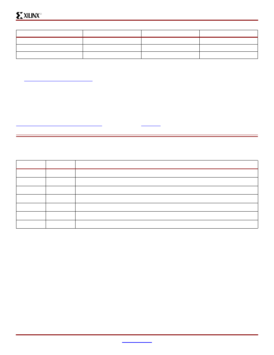
As shown in
, logic density of the XC9500 devices
ranges from 800 to over 6,400 usable gates with 36 to 288
registers, respectively. Multiple package options and asso-
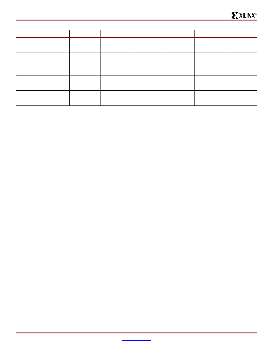
ciated I/O capacity are shown in
. The XC9500 fam-
ily is fully pin-compatible allowing easy design migration
across multiple density options in a given package footprint.
The XC9500 architectural features address the require-
ments of in-system programmability. Enhanced pin-locking
capability avoids costly board rework. An expanded JTAG
instruction set allows version control of programming pat-
terns and in-system debugging. In-system programming
throughout the full device operating range and a minimum
of 10,000 program/erase cycles provide worry-free recon-
figurations and system field upgrades.
Advanced system features include output slew rate control
and user-programmable ground pins to help reduce system
noise. I/Os may be configured for 3.3V or 5V operation. All
outputs provide 24 mA drive.
0
XC9500 In-System Programmable
CPLD Family
DS063 (v5.4) April 3, 2006
0
0
Product Specification
R
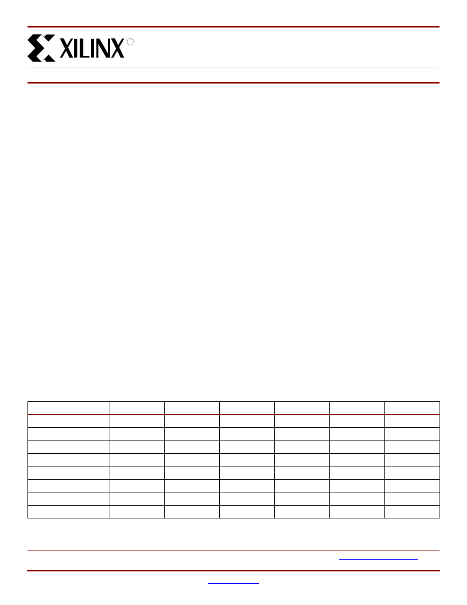
Table 1: XC9500 Device Family
XC9536
XC9572
XC95108
XC95144
XC95216
XC95288
Macrocells
36
72
108
144
216
288
Usable Gates
800
1,600
2,400
3,200
4,800
6,400
Registers
36
72
108
144
216
288
T
PD
(ns)
5
7.5
7.5
7.5
10
15
T
SU
(ns)
3.5
4.5
4.5
4.5
6.0
8.0
T
CO
(ns)
4.0
4.5
4.5
4.5
6.0
8.0
f
CNT
(MHz)
(1)
100
125
125
125
111.1
92.2
f
SYSTEM
(MHz)
(2)
100
83.3
83.3
83.3
66.7
56.6
1.
f
CNT
= Operating frequency for 16-bit counters.
2.
f
SYSTEM
= Internal operating frequency for general purpose system designs spanning multiple FBs.
XC9500 In-System Programmable CPLD Family
2
DS063 (v5.4) April 3, 2006
Product Specification
R
Architecture Description
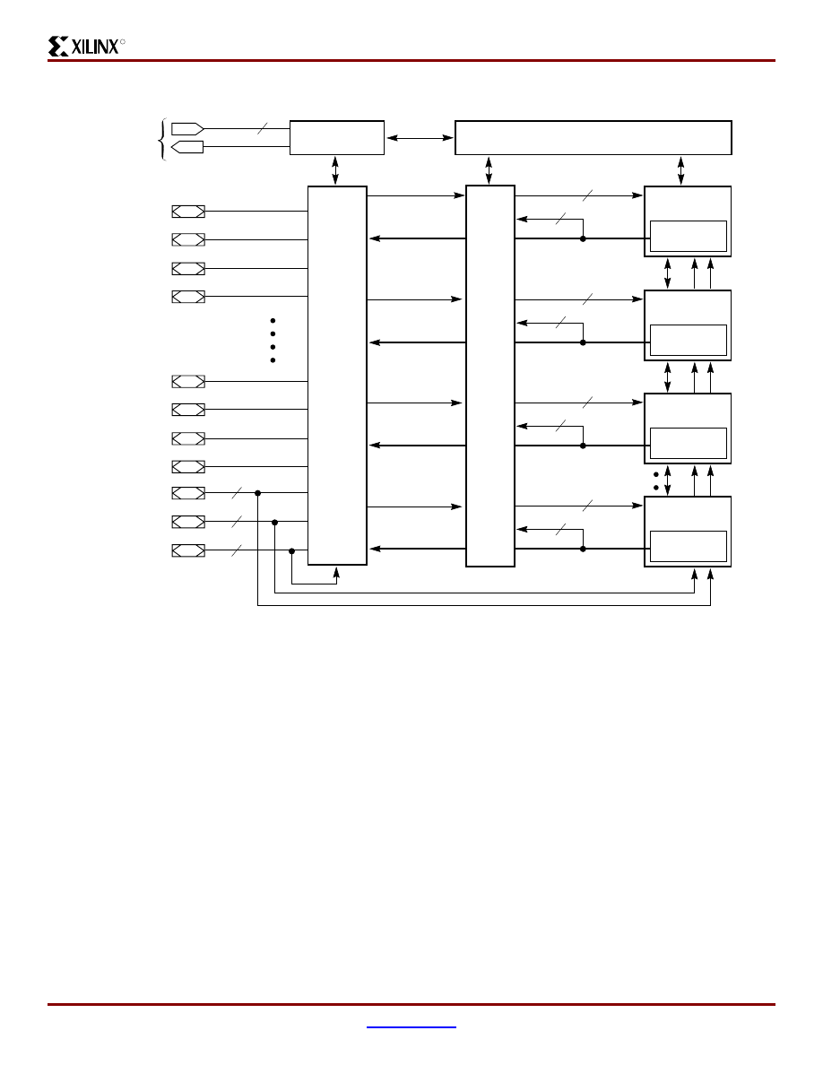
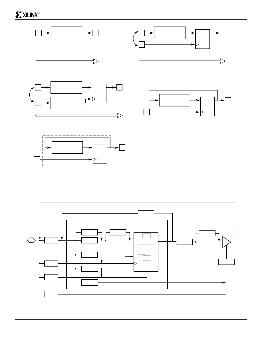
Each XC9500 device is a subsystem consisting of multiple
Function Blocks (FBs) and I/O Blocks (IOBs) fully intercon-
nected by the Fast CONNECT™ switch matrix. The IOB
provides buffering for device inputs and outputs. Each FB
provides programmable logic capability with 36 inputs and
18 outputs. The Fast CONNECT switch matrix connects all
FB outputs and input signals to the FB inputs. For each FB,
12 to 18 outputs (depending on package pin-count) and
Table 2: Available Packages and Device I/O Pins (not including dedicated JTAG pins)
XC9536
XC9572
XC95108
XC95144
XC95216
XC95288
44-Pin VQFP
34
-
-
-
-
-
44-Pin PLCC
34
34
-
-
-
-
48-Pin CSP
34
-
-
-
-
-
84-Pin PLCC
-
69
69
-
-
-
100-Pin TQFP
-
72
81
81
-
-
100-Pin PQFP
-
72
81
81
-
-
160-Pin PQFP
-
-
108
133
133
-
208-Pin HQFP
-
-
-
-
166
168
352-Pin BGA
-
-
-
-
166
192
1.
Most packages available in Pb-Free option. See individual data sheets for more details.
XC9500 In-System Programmable CPLD Family
DS063 (v5.4) April 3, 2006
3
Product Specification
R
associated output enable signals drive directly to the IOBs.
See
Function Block
Each Function Block, as shown in
, is comprised of
18 independent macrocells, each capable of implementing
a combinatorial or registered function. The FB also receives
global clock, output enable, and set/reset signals. The FB
generates 18 outputs that drive the Fast CONNECT switch
matrix. These 18 outputs and their corresponding output
enable signals also drive the IOB.
Logic within the FB is implemented using a sum-of-products
representation. Thirty-six inputs provide 72 true and com-
plement signals into the programmable AND-array to form
90 product terms. Any number of these product terms, up to
the 90 available, can be allocated to each macrocell by the
product term allocator.
Each FB (except for the XC9536) supports local feedback
paths that allow any number of FB outputs to drive into its
own programmable AND-array without going outside the
FB. These paths are used for creating very fast counters
and state machines where all state registers are within the
same FB.
Figure 1: XC9500 Architecture
Note: Function block outputs (indicated by the bold lines) drive the I/O blocks directly.
In-System Programming Controller
JTAG
Controller
I/O
Blocks
Function
Block 1
Macrocells
1 to 18
Macrocells
1 to 18
Macrocells
1 to 18
Macrocells
1 to 18
JTAG Port
3
36
I/O/GTS
I/O/GSR
I/O/GCK
I/O
I/O
I/O
I/O
2 or 4
1
I/O
I/O
I/O
I/O
3
DS063_01_110501
Function
Block 2
36
Function
Block 3
36
18
18
18
18
Function
Block N
36
Fast CONNECT II Switch Matrix
XC9500 In-System Programmable CPLD Family
4
DS063 (v5.4) April 3, 2006
Product Specification
R
Figure 2: XC9500 Function Block
Macrocell 18
Macrocell 1
Programmable
AND-Array
Product
Term
Allocators
From
Fast CONNECT II
Switch Matrix
DS063_02_110501
36
1
To Fast CONNECT II
Switch Matrix
To I/O Blocks
OUT
Global
Set/Reset
3
18
PTOE
18
18
Global
Clocks
XC9500 In-System Programmable CPLD Family
DS063 (v5.4) April 3, 2006
5
Product Specification
R
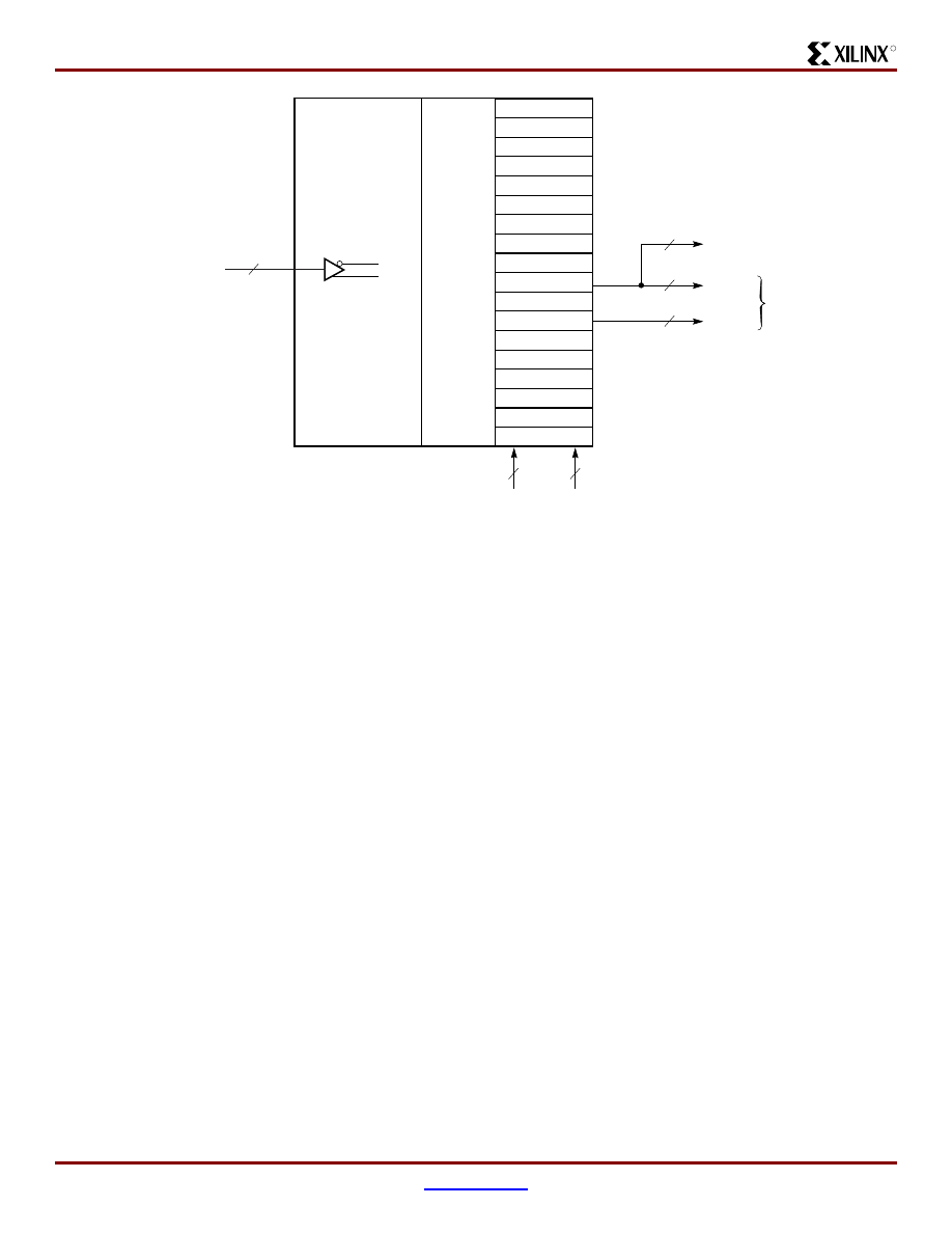
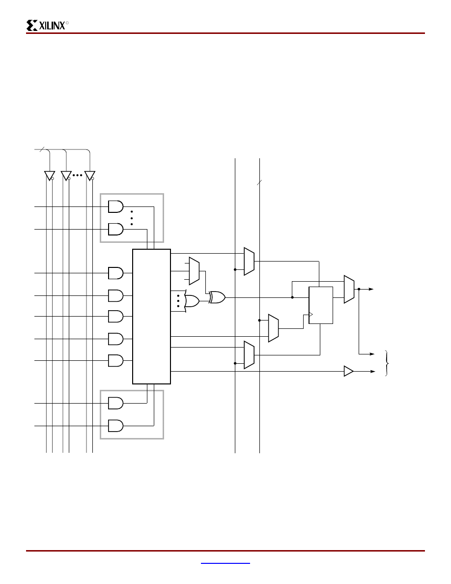
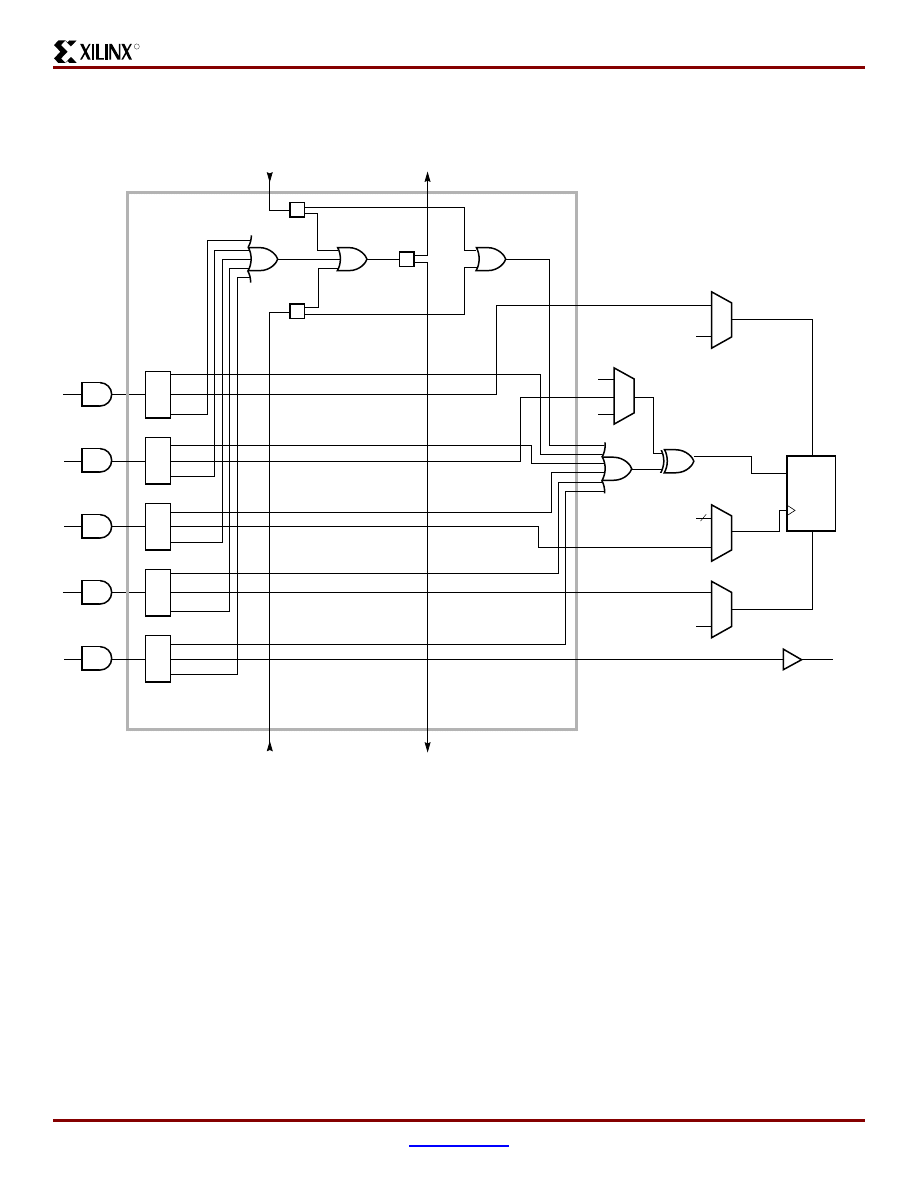
Macrocell
Each XC9500 macrocell may be individually configured for
a combinatorial or registered function. The macrocell and
associated FB logic is shown in
.
Five direct product terms from the AND-array are available
for use as primary data inputs (to the OR and XOR gates) to
implement combinatorial functions, or as control inputs
including clock, set/reset, and output enable. The product
term allocator associated with each macrocell selects how
the five direct terms are used.
The macrocell register can be configured as a D-type or
T-type flip-flop, or it may be bypassed for combinatorial
operation. Each register supports both asynchronous set
and reset operations. During power-up, all user registers
are initialized to the user-defined preload state (default to 0
if unspecified).
Figure 3: XC9500 Macrocell Within Function Block
DS063_03_110501
To
Fast CONNECTII
Switch Matrix
Additional
Product
Terms
(from other
macrocells)
Global
Set/Reset
Global
Clocks
Additional
Product
Terms
(from other
macrocells)
To
I/O Blocks
OUT
1
0
36
3
PTOE
D/T
Q
S
R
Product
Term
Allocator
Product Term Set
Product Term Clock
Product Term Reset
Product Term OE
XC9500 In-System Programmable CPLD Family
6
DS063 (v5.4) April 3, 2006
Product Specification
R
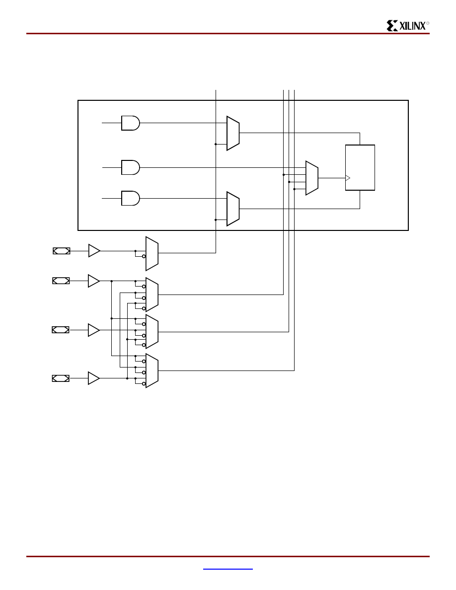
All global control signals are available to each individual
macrocell, including clock, set/reset, and output enable sig-
nals. As shown in
, the macrocell register clock
originates from either of three global clocks or a product
term clock. Both true and complement polarities of a GCK
pin can be used within the device. A GSR input is also pro-
vided to allow user registers to be set to a user-defined
state.
Figure 4: Macrocell Clock and Set/Reset Capability
D/T
S
R
Macrocell
DS063_04_110501
I/O/GSR
Product Term Set
Product Term Clock
Product Term Reset
Global Set/Reset
Global Clock 1
Global Clock 2
Global Clock 3
I/O/GCK3
I/O/GCK2
I/O/GCK1
XC9500 In-System Programmable CPLD Family
DS063 (v5.4) April 3, 2006
7
Product Specification
R
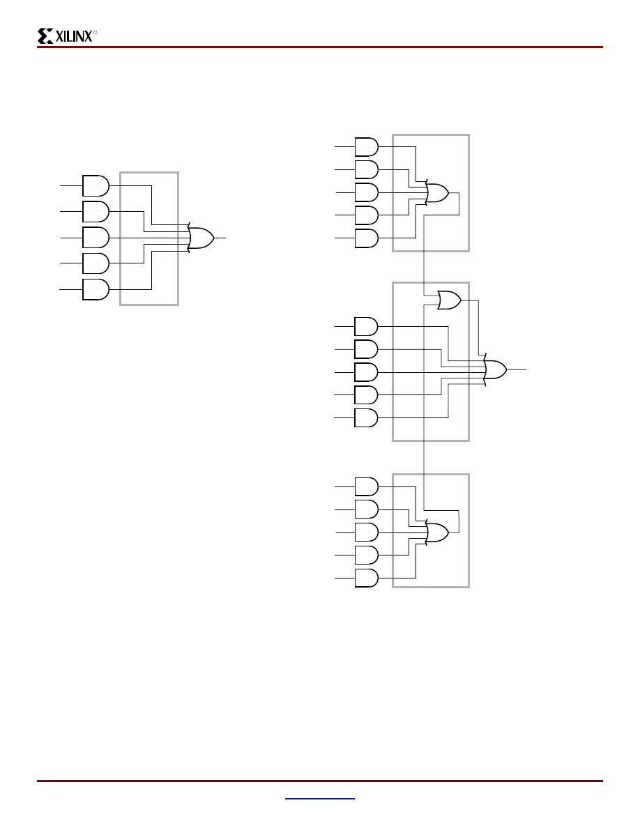
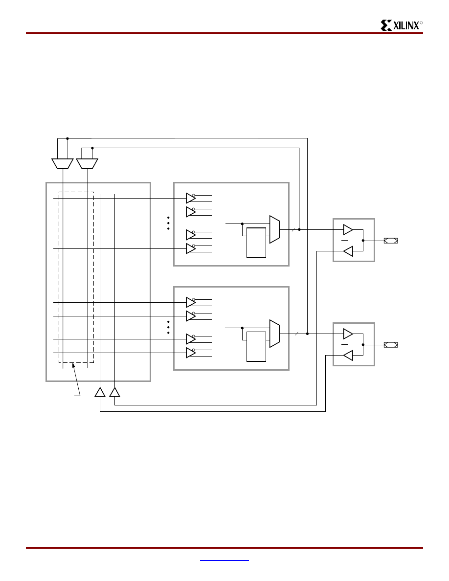
Product Term Allocator
The product term allocator controls how the five direct prod-
uct terms are assigned to each macrocell. For example, all
five direct terms can drive the OR function as shown in
The product term allocator can re-assign other product
terms within the FB to increase the logic capacity of a mac-
rocell beyond five direct terms. Any macrocell requiring
additional product terms can access uncommitted product
terms in other macrocells within the FB. Up to 15 product
terms can be available to a single macrocell with only a
small incremental delay of T
PTA,
as shown in
.
Note that the incremental delay affects only the product
terms in other macrocells. The timing of the direct product
terms is not changed.
Figure 5: Macrocell Logic Using Direct Product Term
Product Term
Allocator
Macrocell
Product Term
Logic
DS063_05_110501
Figure 6: Product Term Allocation With 15 Product
Terms
Macrocell Logic
With 15
Product Terms
Product Term
Allocator
Product Term
Allocator
DS063_06_110501
Product Term
Allocator
XC9500 In-System Programmable CPLD Family
8
DS063 (v5.4) April 3, 2006
Product Specification
R
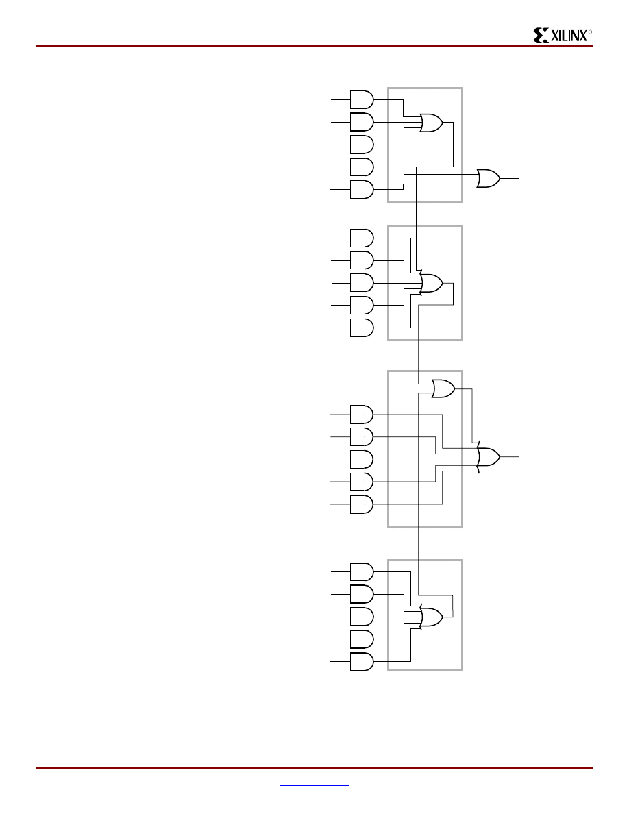
The product term allocator can re-assign product terms
from any macrocell within the FB by combining partial sums
of products over several macrocells, as shown in
.
In this example, the incremental delay is only 2
*
T
PTA
. All 90
product terms are available to any macrocell, with a maxi-
mum incremental delay of 8
*
T
PTA.
Figure 7: Product Term Allocation Over Several
Macrocells
Macrocell Logic
With 18
Product Terms
Macrocell Logic
With 2
Product Terms
Product Term
Allocator
Product Term
Allocator
DS063_07 _110501
Product Term
Allocator
Product Term
Allocator
XC9500 In-System Programmable CPLD Family
DS063 (v5.4) April 3, 2006
9
Product Specification
R
The internal logic of the product term allocator is shown in
Figure 8: Product Term Allocator Logic
D/T Q
S
R
From Upper
Macrocell
To Upper
Macrocell
Product Term Set
Product Term Clock
Product Term Reset
Global Set/Reset
Global Set/Reset
Global Clocks
Product Term OE
Product Term
Allocator
To Lower
Macrocell
From Lower
Macrocell
DS063_08_110501
1
0
XC9500 In-System Programmable CPLD Family
10
DS063 (v5.4) April 3, 2006
Product Specification
R
Fast CONNECT Switch Matrix
The Fast CONNECT switch matrix connects signals to the
FB inputs, as shown in
. All IOB outputs (corre-
sponding to user pin inputs) and all FB outputs drive the
Fast CONNECT matrix. Any of these (up to a FB fan-in limit
of 36) may be selected, through user programming, to drive
each FB with a uniform delay.
The Fast CONNECT switch matrix is capable of combining
multiple internal connections into a single wired-AND output
before driving the destination FB. This provides additional
logic capability and increases the effective logic fan-in of the
destination FB without any additional timing delay. This
capability is available for internal connections originating
from FB outputs only. It is automatically invoked by the
development software where applicable.
Figure 9: Fast CONNECT Switch Matrix
DS063_09_110501
Function Block
Fast CONNECT
Switch Matrix
(36)
I/O
Function Block
Wired-AND
Capability
I/O Block
18
18
I/O Block
(36)
I/O
D/T Q
D/T Q
XC9500 In-System Programmable CPLD Family
DS063 (v5.4) April 3, 2006
Product Specification
R
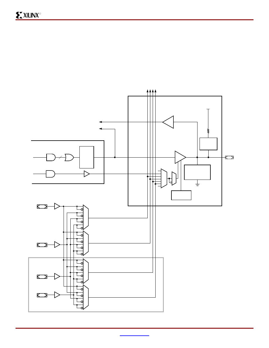
I/O Block
The I/O Block (IOB) interfaces between the internal logic
and the device user I/O pins. Each IOB includes an input
buffer, output driver, output enable selection multiplexer,
and user programmable ground control. See
details.
The input buffer is compatible with standard 5V CMOS, 5V
TTL, and 3.3V signal levels. The input buffer uses the internal
5V voltage supply (V
CCINT
) to ensure that the input thresh-
olds are constant and do not vary with the V
CCIO
voltage.
The output enable may be generated from one of four
options: a product term signal from the macrocell, any of the
global OE signals, always [1], or always [0]. There are two
global output enables for devices with up to 144 macrocells,
and four global output enables for the rest of the devices.
Both polarities of any of the global 3-state control (GTS)
pins may be used within the device..
Figure 10: I/O Block and Output Enable Capability
I/O Block
Macrocell
DS063_10_092203
Product Term OE
PTOE
Switch Matrix
OUT
(Inversion in
AND-array)
Global OE 1
1
To other
Macrocells
Slew Rate
Control
0
Global OE 2
Available in
XC95216
and XC95288
Global OE 3
Global OE 4
I/O/GTS1
I/O
I/O/GTS2
I/O/GTS3
I/O/GTS4
To Fast CONNECT
User-
Programmable
Ground
Pull-up
Resistor*
V
CCIO
XC9500 In-System Programmable CPLD Family
12
DS063 (v5.4) April 3, 2006
Product Specification
R
Each output has independent slew rate control. Output
edge rates may be slowed down to reduce system noise
(with an additional time delay of T
SLEW
) through program-
ming. See
Each IOB provides user programmable ground pin capabil-
ity. This allows device I/O pins to be configured as additional
ground pins. By tying strategically located programmable
ground pins to the external ground connection, system
noise generated from large numbers of simultaneous
switching outputs may be reduced.
A control pull-up resistor (typically 10K ohms) is attached to
each device I/O pin to prevent them from floating when the
device is not in normal user operation. This resistor is active
during device programming mode and system power-up. It
is also activated for an erased device. The resistor is deac-
tivated during normal operation.
The output driver is capable of supplying 24 mA output
drive. All output drivers in the device may be configured for
either 5V TTL levels or 3.3V levels by connecting the device
output voltage supply (V
CCIO
) to a 5V or 3.3V voltage sup-
ply.
shows how the XC9500 device can be used
in 5V only and mixed 3.3V/5V systems.
Pin-Locking Capability
The capability to lock the user defined pin assignments dur-
ing design changes depends on the ability of the architec-
ture to adapt to unexpected changes. The XC9500 devices
have architectural features that enhance the ability to
accept design changes while maintaining the same pinout.
The XC9500 architecture provides maximum routing within
the Fast CONNECT switch matrix, and incorporates a flexi-
ble Function Block that allows block-wide allocation of avail-
able product terms. This provides a high level of confidence
of maintaining both input and output pin assignments for
unexpected design changes.
For extensive design changes requiring higher logic capac-
ity than is available in the initially chosen device, the new
design may be able to fit into a larger pin-compatible device
using the same pin assignments. The same board may be
used with a higher density device without the expense of
board rework
Figure 11: Output slew-Rate for (a) Rising and (b) Falling Outputs
Figure 12: XC9500 Devices in (a) 5V Systems and (b) Mixed 5V/3.3V Systems
Time
0
0
1.5V
Standard
Output
Voltage
(a)
Slew-Rate Limited
Time
Output
Voltage
(b)
Standard
Slew-Rate Limited
T
SLEW
T
SLEW
1.5V
DS063_11_110501
IN
OUT
5V
GND
(b)
3.3V
XC9500
CPLD
V
CCINT
V
CCIO
5V
0V
3.3V
0V
3.6V
0V
3.3V
0V
3.3V
DS063_12_110501
3.3V
5V TTL or
5V CMOS or
IN
OUT
5V
GND
(a)
5V TTL
XC9500
CPLD
V
CCINT
V
CCIO
5V
0V
–4V
0V
3.6V
0V
3.3V
0V
3.3V
5V TTL or
5V CMOS or
XC9500 In-System Programmable CPLD Family
DS063 (v5.4) April 3, 2006
Product Specification
R
In-System Programming
XC9500 devices are programmed in-system via a standard
4-pin JTAG protocol, as shown in
. In-system pro-
gramming offers quick and efficient design iterations and
eliminates package handling. The Xilinx development sys-
tem provides the programming data sequence using a Xilinx
download cable, a third-party JTAG development system,
JTAG-compatible board tester, or a simple microprocessor
interface that emulates the JTAG instruction sequence.
All I/Os are 3-stated and pulled high by the IOB resistors
during in-system programming. If a particular signal must
remain Low during this time, then a pulldown resistor may
be added to the pin.
External Programming
XC9500 devices can also be programmed by the Xilinx
HW130 device programmer as well as third-party program-
mers. This provides the added flexibility of using pre-pro-
grammed devices during manufacturing, with an in-system
programmable option for future enhancements.
Endurance
All XC9500 CPLDs provide a minimum endurance level of
10,000 in-system program/erase cycles. Each device meets
all functional, performance, and data retention specifica-
tions within this endurance limit.
IEEE 1149.1 Boundary-Scan (JTAG)
XC9500 devices fully support IEEE 1149.1 boundary-scan
(JTAG). EXTEST, SAMPLE/PRELOAD, BYPASS, USER-
CODE, INTEST, IDCODE, and HIGHZ instructions are sup-
ported in each device. For ISP operations, five additional
instructions are added; the ISPEN, FERASE, FPGM, FVFY,
and ISPEX instructions are fully compliant extensions of the
1149.1 instruction set.
The TMS and TCK pins have dedicated pull-up resistors as
specified by the IEEE 1149.1 standard.
Boundary Scan Description Language (BSDL) files for the
XC9500 are included in the development system and are
available on the Xilinx FTP site.
Design Security
XC9500 devices incorporate advanced data security fea-
tures which fully protect the programming data against
unauthorized reading or inadvertent device erasure/repro-
gramming.
shows the four different security settings
available.
The read security bits can be set by the user to prevent the
internal programming pattern from being read or copied.
When set, they also inhibit further program operations but
allow device erase. Erasing the entire device is the only way
to reset the read security bit.
The write security bits provide added protection against
accidental device erasure or reprogramming when the
JTAG pins are subject to noise, such as during system
power-up. Once set, the write-protection may be deacti-
vated when the device needs to be reprogrammed with a
valid pattern.
Table 3: Data Security Options
Read Security
Default
Set
W
rite Security
Default
Read Allowed
Program/Erase
Allowed
Read Inhibited
Program Inhibited
Erase Allowed
Set
Read Allowed
Program/Erase
Inhibited
Read Inhibited
Program/Erase
Inhibited
XC9500 In-System Programmable CPLD Family
14
DS063 (v5.4) April 3, 2006
Product Specification
R
Low Power Mode
All XC9500 devices offer a low-power mode for individual
macrocells or across all macrocells. This feature allows the
device power to be significantly reduced.
Each individual macrocell may be programmed in
low-power mode by the user. Performance-critical parts of
the application can remain in standard power mode, while
other parts of the application may be programmed for
low-power operation to reduce the overall power dissipa-
tion. Macrocells programmed for low-power mode incur
additional delay (T
LP
) in pin-to-pin combinatorial delay as
well as register setup time. Product term clock to output and
product term output enable delays are unaffected by the
macrocell power-setting.
Timing Model
The uniformity of the XC9500 architecture allows a simpli-
fied timing model for the entire device. The basic timing
model, shown in
, is valid for macrocell functions
that use the direct product terms only, with standard power
setting, and standard slew rate setting.
shows how
each of the key timing parameters is affected by the product
term allocator (if needed), low-power setting, and slew-lim-
ited setting.
The product term allocation time depends on the logic span
of the macrocell function, which is defined as one less than
the maximum number of allocators in the product term path.
If only direct product terms are used, then the logic span is
0. The example in
shows that up to 15 product
terms are available with a span of 1. In the case of
the 18 product term function has a span of 2.
Detailed timing information may be derived from the full tim-
ing model shown in
. The values and explanations
for each parameter are given in the individual device data
sheets.
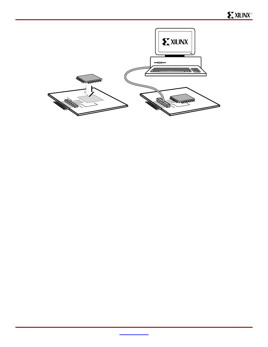
Figure 13: In-System Programming Operation (a) Solder Device to PCB and (b) Program Using Download Cable
X5902
GND
V
CC
(a)
(b)
XC9500 In-System Programmable CPLD Family
DS063 (v5.4) April 3, 2006
15
Product Specification
R
Figure 14: Basic Timing Model
Figure 15: Detailed Timing Model
Combinatorial
Logic
Propagation Delay = T
PD
(a)
Combinatorial
Logic
Setup Time = T
SU
T
CO
T
PSU
T
PCO
Clock to Out Time = T
CO
(b)
D/T Q
Combinatorial
Logic
Internal System Cycle Time = T
SYSTEM
DS063_14_110501
(d)
D/T Q
Combinatorial
Logic
Setup Time = T
PSU
Clock to Out Time = T
PCO
(c)
P-Term Clock
Path
D/T Q
Combinatorial
Logic
All resources within FB using local Feedback
Internal Cycle Time = T
CNT
(e)
D/T Q
D/T
Q
SR
T
IN
T
LOGILP
S*T
PTA
Pin Feedback
T
F
T
PDI
T
SUI
T
COI
T
HI
T
AOI
T
RAI
T
OUT
T
SLEW
T
EN
DS063_15_110501
T
LOGI
T
PTCK
T
PTSR
T
PTTS
T
GCK
T
GSR
T
GTS
Macrocell
EC
XC9500 In-System Programmable CPLD Family
16
DS063 (v5.4) April 3, 2006
Product Specification
R
Power-Up Characteristics
The XC9500 devices are well behaved under all operating
conditions. During power-up each XC9500 device employs
internal circuitry which keeps the device in the quiescent
state until the V
CCINT
supply voltage is at a safe level
(approximately 3.8V). During this time, all device pins and
JTAG pins are disabled and all device outputs are disabled
with the IOB pull-up resistors (~10K ohms) enabled, as
shown in
. When the supply voltage reaches a safe
level, all user registers become initialized (typically within
100
μs for 9536, 95144, 200 μs for 95216, and 300 μs for
95288), and the device is immediately available for opera-
tion, as shown in
.
If the device is in the erased state (before any user pattern
is programmed), the device outputs remain disabled with
the IOB pull-up resistors enabled. The JTAG pins are
enabled to allow the device to be programmed at any time.
If the device is programmed, the device inputs and outputs
take on their configured states for normal operation. The
JTAG pins are enabled to allow device erasure or bound-
ary-scan tests at any time.
Development System Support
The XC9500 CPLD family is fully supported by the develop-
ment systems available from Xilinx and the Xilinx Alliance
Program vendors.
The designer can create the design using ABEL, schemat-
ics, equations, VHDL, or Verilog in a variety of software
front-end tools. The development system can be used to
implement the design and generate a JEDEC bitmap which
can be used to program the XC9500 device. Each develop-
ment system includes JTAG download software that can be
used to program the devices via the standard JTAG inter-
face and a download cable.
FastFLASH Technology
An advanced CMOS Flash process is used to fabricate all
XC9500 devices. Specifically developed for Xilinx in-system
programmable CPLDs, the FastFLASH process provides
high performance logic capability, fast programming times,
and endurance of 10,000 program/erase cycles.
Figure 16: Device Behavior During Power-up
V
CCINT
No
Power
3.8 V
(Typ)
0V
No
Power
Quiescent
State
Quiescent
State
User Operation
Initialization of User Registers
DS063_16_110501
3.8V
(Typ)
Table 4: Timing Model Parameters
Parameter
Description
Product Term
Allocator
(1)
Macrocell
Low-Power Setting
Output
Slew-Limited
Setting
T
PD
Propagation Delay
+ T
PTA
*
S
+ T
LP
+ T
SLEW
T
SU
Global Clock Setup Time
+ T
PTA
*
S
+ T
LP
–
T
CO
Global Clock-to-output
-
-
+ T
SLEW
T
PSU
Product Term Clock Setup Time
+ T
PTA
*
S
+ T
LP
-
T
PCO
Product Term Clock-to-output
-
-
+ T
SLEW
T
SYSTEM
Internal System Cycle Period
+ T
PTA
*
S
+ T
LP
-
Notes:
1.
S = the logic span of the function, as defined in the text.
Table 5: XC9500 Device Characteristics
Device Circuitry
Quiescent State
Erased Device Operation
Valid User Operation
IOB Pull-up Resistors
Enabled
Enabled
Disabled
Device Outputs
Disabled
Disabled
As Configured
XC9500 In-System Programmable CPLD Family
DS063 (v5.4) April 3, 2006
17
Product Specification
R
Warranty Disclaimer
THESE PRODUCTS ARE SUBJECT TO THE TERMS OF THE XILINX LIMITED WARRANTY WHICH CAN BE VIEWED
AT
http://www.xilinx.com/warranty.htm
. THIS LIMITED WARRANTY DOES NOT EXTEND TO ANY USE OF THE
PRODUCTS IN AN APPLICATION OR ENVIRONMENT THAT IS NOT WITHIN THE SPECIFICATIONS STATED ON THE
THEN-CURRENT XILINX DATA SHEET FOR THE PRODUCTS. PRODUCTS ARE NOT DESIGNED TO BE FAIL-SAFE
AND ARE NOT WARRANTED FOR USE IN APPLICATIONS THAT POSE A RISK OF PHYSICAL HARM OR LOSS OF
LIFE. USE OF PRODUCTS IN SUCH APPLICATIONS IS FULLY AT THE RISK OF CUSTOMER SUBJECT TO
APPLICABLE LAWS AND REGULATIONS.
Additional Information
XC9500 Data sheets and application notes.
Revision History
The following table shows the revision history for this document.
Device Inputs and Clocks
Disabled
Disabled
As Configured
Function Block
Disabled
Disabled
As Configured
JTAG Controller
Disabled
Enabled
Enabled
Table 5: XC9500 Device Characteristics
Device Circuitry
Quiescent State
Erased Device Operation
Valid User Operation
Date
Version
Revision
3.0
12/14/98
Revised datasheet to reflect new AC characteristics and Internal Timing Parmeters.
4.0
02/10/99
Corrected Figure 3.
5.0
09/15/99
Added -10 speed grade to XC95288.
5.1
09/22/03
Minor edits.
5.2
02/16/04
Corrected statement on GTS inputs on page 10. Added links to additional information.
5.3
04/15/05
Update to PDF attributes only. No changes to documentation.
5.4
04/03/06
Added Warranty Disclaimer. Added note on Pb-Free packages.
Document Outline
- Features
- Family Overview
- Architecture Description
- Function Block
- Macrocell
- Pin-Locking Capability
- In-System Programming
- Endurance
- IEEE 1149.1 Boundary-Scan (JTAG)
- Design Security
- Low Power Mode
- Timing Model
- Power-Up Characteristics
- Development System Support
- FastFLASH Technology
- Warranty Disclaimer
- Additional Information
- Revision History
Wyszukiwarka
Podobne podstrony:
DS066 XC95108 In System Programmable CPLD
In System Programming T89C51RD2 Bootloader
AL2 system i programowanie pl
Botanika systematyczna program ćwiczeń 2014, biologia, Biologia I rok, Botanika systematyczna
zaawansowane systemy programowania grafiki
System programowego oddziaływania
William Weber From miscellany to homogenity in Concert Programming
SYSTEM PROGRAMOWANEGO ODDZIAŁYWANIA W OPINIACH WIĘŹNIÓW
Static Detection of Malicious Code in Executable Programs
Flora Polski systematyka i program do cwiczen(1)
Teffaha D Relevance of Water Gymnastics in Rehabilitation Programs in
O'Reilly Programming Embedded Systems in C and C
Self Study Programme 351 Common rail fuel injection system fitted in the 3 0l V6 TDI engine
zarzadzenie nr 97 prezesa rady ministrow w sprawie utworzenia zespolu ds realizacji rzadowego progra
alcatel support document for cable system in cuba
więcej podobnych podstron