L4: 6.111 Spring 2006
1
Introductory Digital Systems Laboratory
L4: Sequential Building Blocks
L4: Sequential Building Blocks
(Flip
(Flip
-
-
flops, Latches and Registers)
flops, Latches and Registers)
Acknowledgements:
J. Rabaey, A. Chandrakasan, B. Nikolic. Digital Integrated Circuits: A Design Perspective.
Prof. Randy Katz (Unified Microelectronics Corporation Distinguished Professor in
Electrical Engineering and Computer Science at the University of California, Berkeley)
and Prof. Gaetano Borriello (University of Washington Department of Computer
Science & Engineering) from Chapter 2 of R. Katz, G. Borriello. Contemporary Logic Design.
Materials in this lecture are courtesy of the following sources and are used with permission.
2nd ed. Prentice-Hall/Pearson Education, 2005.
Prentice Hall/Pearson, 2003.
L4: 6.111 Spring 2006
2
Introductory Digital Systems Laboratory
Combinational Logic Review
Combinational Logic Review
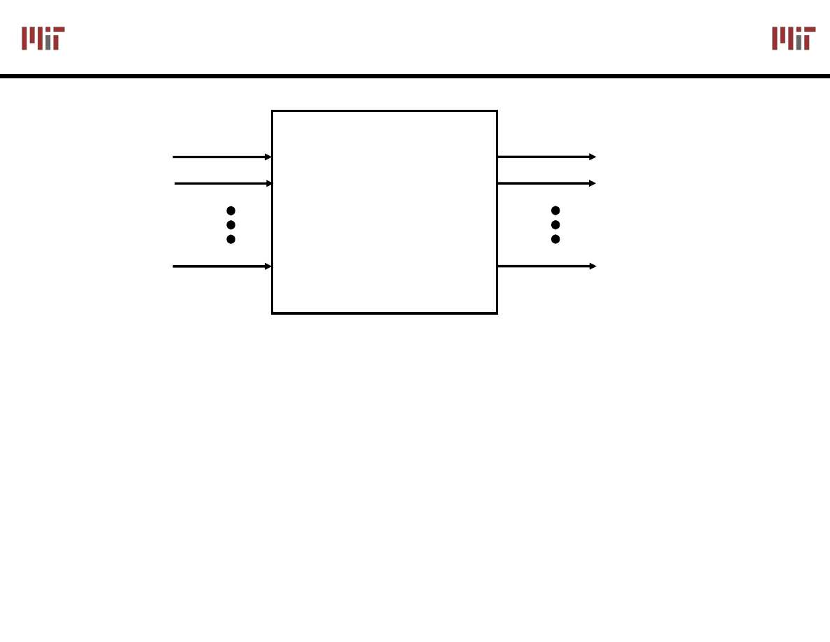
Combinational logic circuits are memoryless
No feedback in combinational logic circuits
Output assumes the function implemented by the
logic network, assuming that the switching
transients have settled
Outputs can have multiple logical transitions
before settling to the correct value
Combinational
Circuit
in
0
in
1
in
N-1
in
0
in
1
in
M-1
L4: 6.111 Spring 2006
3
Introductory Digital Systems Laboratory
A Sequential System
A Sequential System
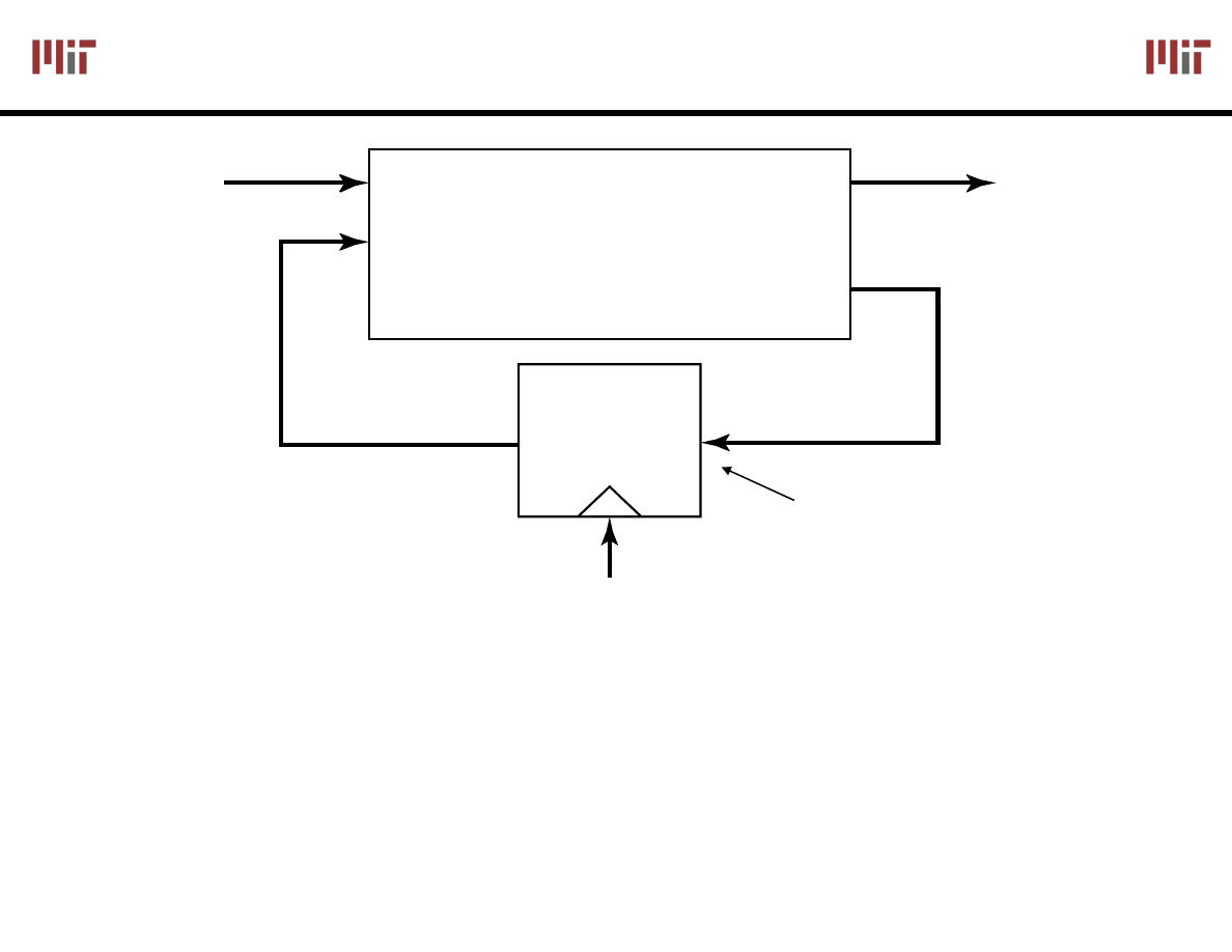
Sequential circuits have memory (i.e., remember the past)
The current state is “held” in memory and the next state is
computed based the current state and the current inputs
In a synchronous systems, the
clock signal
orchestrates the
sequence of events
COMBINATIONAL
LOGIC
Registers
Outputs
Next state
CLK
Q
D
Current State
Inputs
Memory element
L4: 6.111 Spring 2006
4
Introductory Digital Systems Laboratory
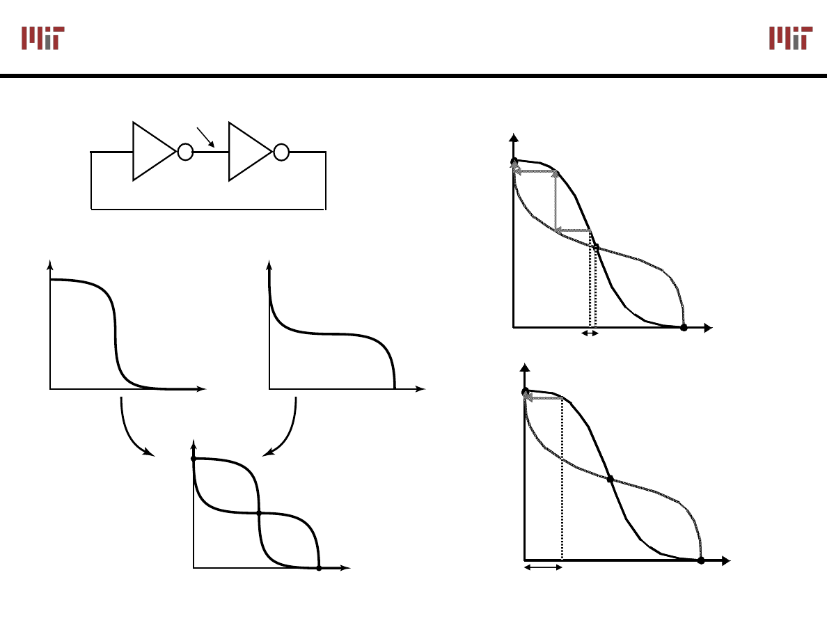
A Simple Example
A Simple Example
in
0
in
1
in
2
in
N-1
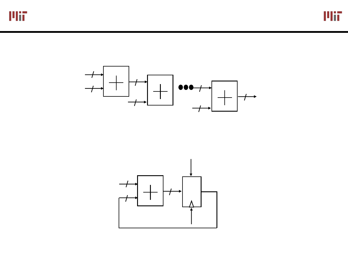
Adding N inputs (N-1 Adders)
in
D Q
reset
clk
Current_Sum
Using a sequential (serial) approach
L4: 6.111 Spring 2006
5
Introductory Digital Systems Laboratory
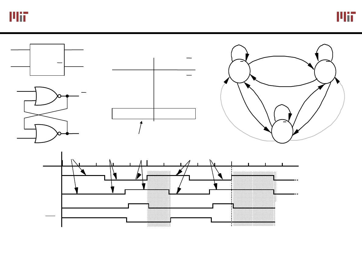
Implementing State: Bi
Implementing State: Bi
-
-
stability
stability
V
i1
A
C
B
V
o2
V
i 1
= V
o2
V
o1
V
i2
V
i 2
= V
o1
V
o1
= V
i2
V
o2
= V
i1
Point C is
Metastable
V
i2
=
V
o
V
i1
= V
o2
A
δ
V
i2
=
V
o
1
V
i1
= V
o2
C
δ
1
Points A and
B are stable
(represent 0 & 1)
B
L4: 6.111 Spring 2006
6
Introductory Digital Systems Laboratory
NOR
NOR
-
-
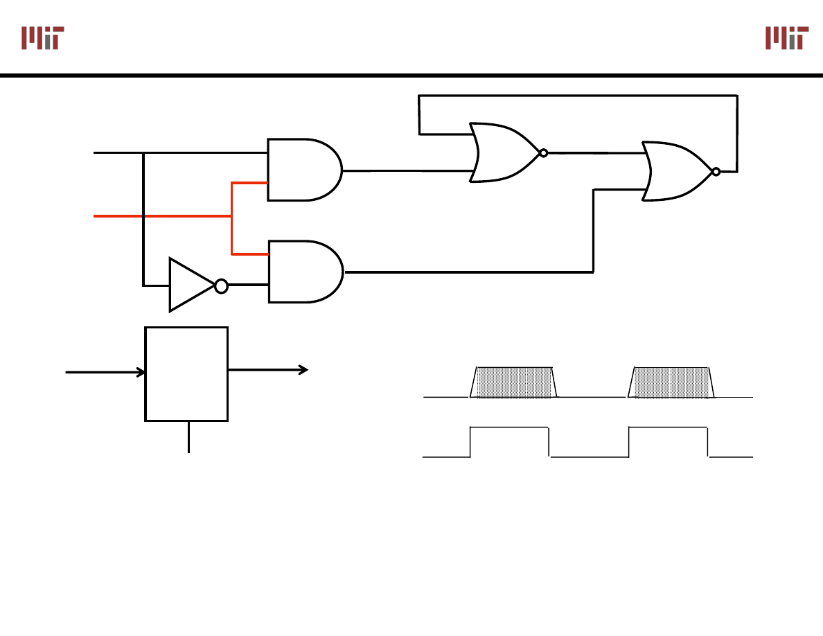
based Set
based Set
-
-
Reset (SR)
Reset (SR)
Flipflop
Flipflop
Flip-flop refers to a bi-stable element
(
edge-triggered registers are also
called flip-flops
) – this circuit is not clocked and outputs change
“asynchronously” with the inputs
Q Q
Q Q
Q Q
0 1
1 0
0 0
SR = 1 0
SR = 0 1
SR = 0 1
SR = 1 1
SR = 1 0
SR = 1 1
SR = 00, 01
SR = 00, 10
SR = 0 0
SR = 11
SR = 0 0
Reset
Hold
Set
Set
Reset
R
S
Q
Q
??
Forbidden State
S
S
R
Q
Q
Q
Q
R
S
Q
0
0
1
0
1
0
1
0
0
1
1
R
Q
Q
Q
0
1
0
L4: 6.111 Spring 2006
7
Introductory Digital Systems Laboratory
Making a Clocked Memory Element:
Making a Clocked Memory Element:
Positive D
Positive D
-
-
Latch
Latch
CLK
D
Q
D
Q
clk
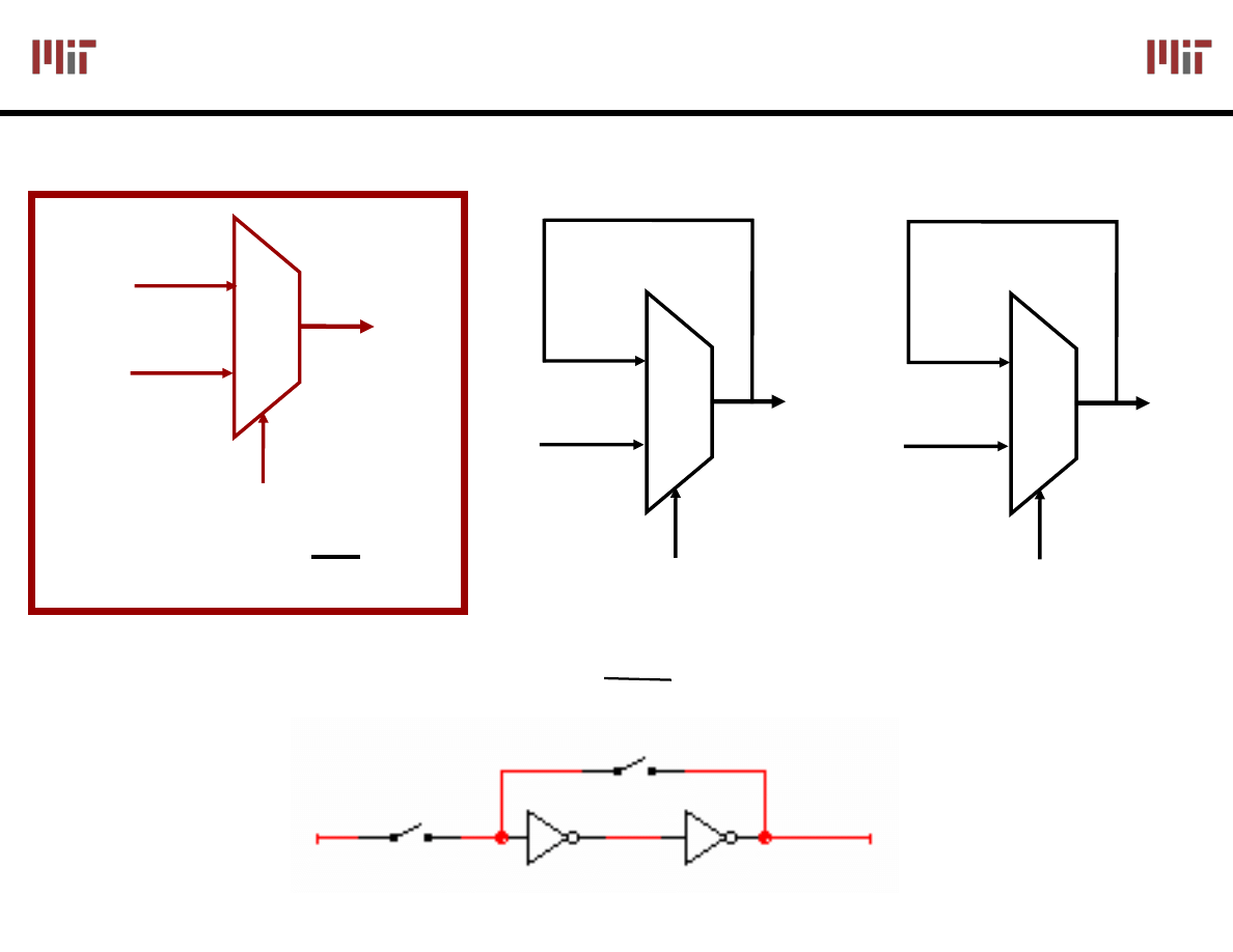
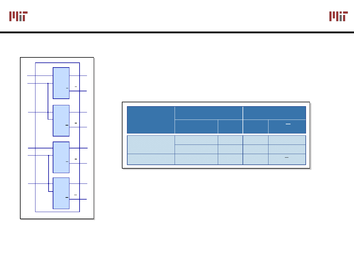
A Positive D-Latch
:
Passes input D to output Q when CLK is
high and holds state when clock is low (i.e., ignores input D)
A Latch is level-sensitive:
invert clock for a negative latch
S
R
clock
R and S
sample
hold
sample
hold
hold
G
L4: 6.111 Spring 2006
8
Introductory Digital Systems Laboratory
Multiplexor
Multiplexor
Based Positive & Negative Latch
Based Positive & Negative Latch
1
0
in
0
in
1
out
SEL
Out = sel * in
1
+ sel * in
0
2:1 multiplexor
1
0
D
Q
CLK
Positive Latch
0
1
D
Q
CLK
Negative Latch
"remember"
"load"
"data"
"stored value"
clk
clk
L4: 6.111 Spring 2006
9
Introductory Digital Systems Laboratory
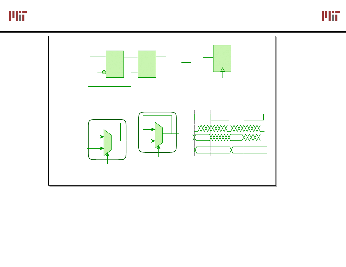
74HC75 (Positive Latch)
74HC75 (Positive Latch)
2
13
1D
1Q
2Q
3Q
4Q
16
LE
1-2
LE
3-4
1Q
2Q
3Q
4Q
1
D
CP
CP
CP
CP
L2
L1
L3
L4
Q
Q
Q
Q
3
2D
3D
15
14
6
4
7
4D
10
11
9
8
Q
D
Q
D
Q
D
Q
Operating Modes
Inputs
Outputs
LE
n-n
nD
nQ
nQ
Data Enabled
Data Latched
H
H
H
L
L
X
q
q
L
H
L
H
Figures by MIT OpenCourseWare.
L4: 6.111 Spring 2006
10
Introductory Digital Systems Laboratory
Building an Edge
Building an Edge
-
-
Triggered Register
Triggered Register
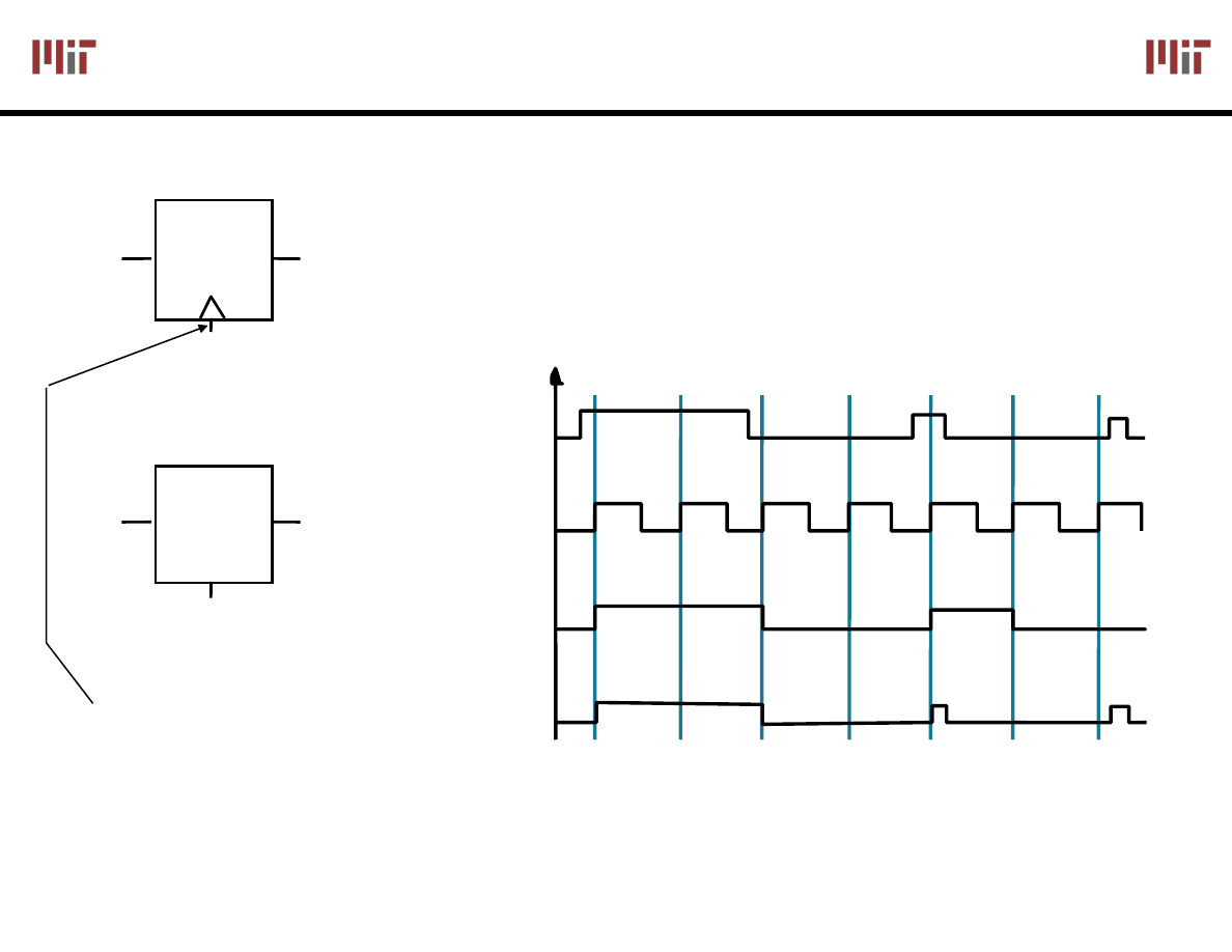
Master-Slave Register
Use negative clock phase to latch inputs into first latch
Use positive clock to change outputs with second latch
View pair as one basic unit
master-slave flip-flop twice as much logic
1
0
D
Master
0
1
Q
Slave
Q
M
Q
M
Q
D
CLK
D
G
Q
D
G
Q
CLK
CLK
CLK
CLK
D
Q
D Q
Q
D
Q
M
Negative latch
Positive latch
Image by MIT OpenCourseWare.
L4: 6.111 Spring 2006
11
Introductory Digital Systems Laboratory
Latches vs. Edge
Latches vs. Edge
-
-
Triggered Register
Triggered Register
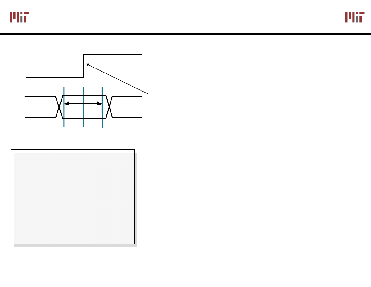
Edge triggered device sample inputs on the event edge
Transparent latches sample inputs as long as the clock is
asserted
Timing Diagram:
Behavior the same unless input changes
while the clock is high
7474
7475
Bubble here
for negative
edge triggered
register
Positive edge-triggered
register
Level-sensitive
latch
D Q
D Q
C
Clk
Clk
D
Clk
Q
Q
7474
7475
L4: 6.111 Spring 2006
12
Introductory Digital Systems Laboratory
Important Timing Parameters
Important Timing Parameters
Setup Time (T
su
)
Clock:
Periodic Event, causes state of memory
element to change
memory element can be updated on the:
rising edge, falling edge, high level, low level
There is a timing
"window" around the
clocking event
during which the
input must remain
stable and
unchanged in order
to be recognized
There is a timing
"window" around the
clocking event
during which the
input must remain
stable and
unchanged in order
to be recognized
Minimum time before the clocking event by
which the input must be stable
Hold Time (T
h
)
Minimum time after the clocking event during
which the input must remain stable
Input
Clock
T
su
T
h
Propagation Delay (T
cq
for an edge-triggered
register and T
dq
for a latch)
Delay overhead of the memory element
L4: 6.111 Spring 2006
13
Introductory Digital Systems Laboratory
The J
The J
-
-
K Flip
K Flip
-
-
Flop
Flop
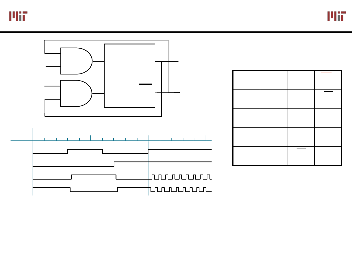
Eliminate the forbidden state of the SR Flip-flop
Use output feedback to guarantee that R and S are
never both one
J
K
Q+
Q+
0
1
0
1
Q
0
1
Q
0
Q
0
1
1
0
1
Q
J
K
Q
\ Q
100
S
R
Q
Q
J
K
L4: 6.111 Spring 2006
14
Introductory Digital Systems Laboratory
J
J
-
-
K Master
K Master
-
-
Slave Register
Slave Register
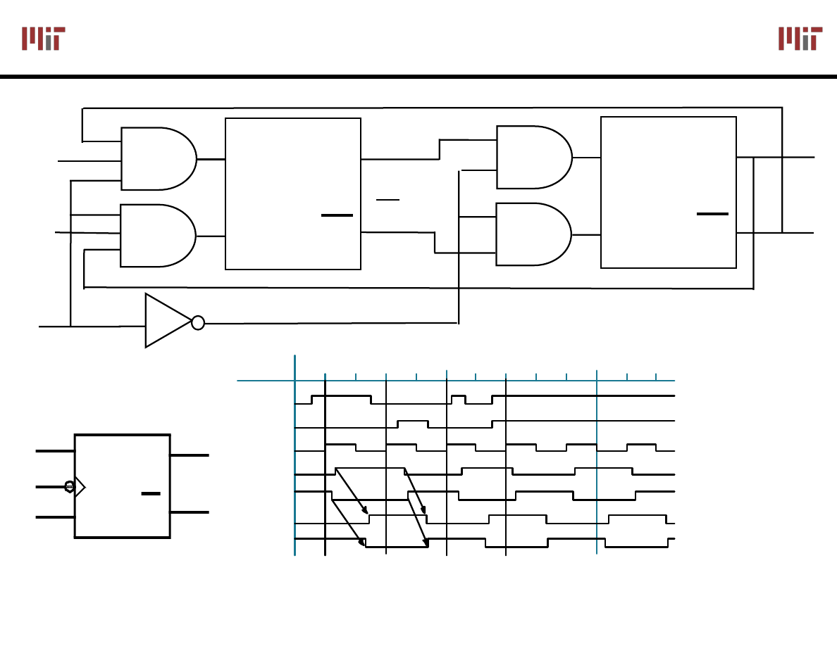
Correct Toggle
Operation
Master
outputs
Slave
outputs
Set Reset
T
oggle
1's
S
R
Q
Q
J
K
S
R
Q
Q
Sample inputs while clock high
Sample inputs while clock low
P
P
Catch
100
J
K
Clk
P
\ P
Q
\ Q
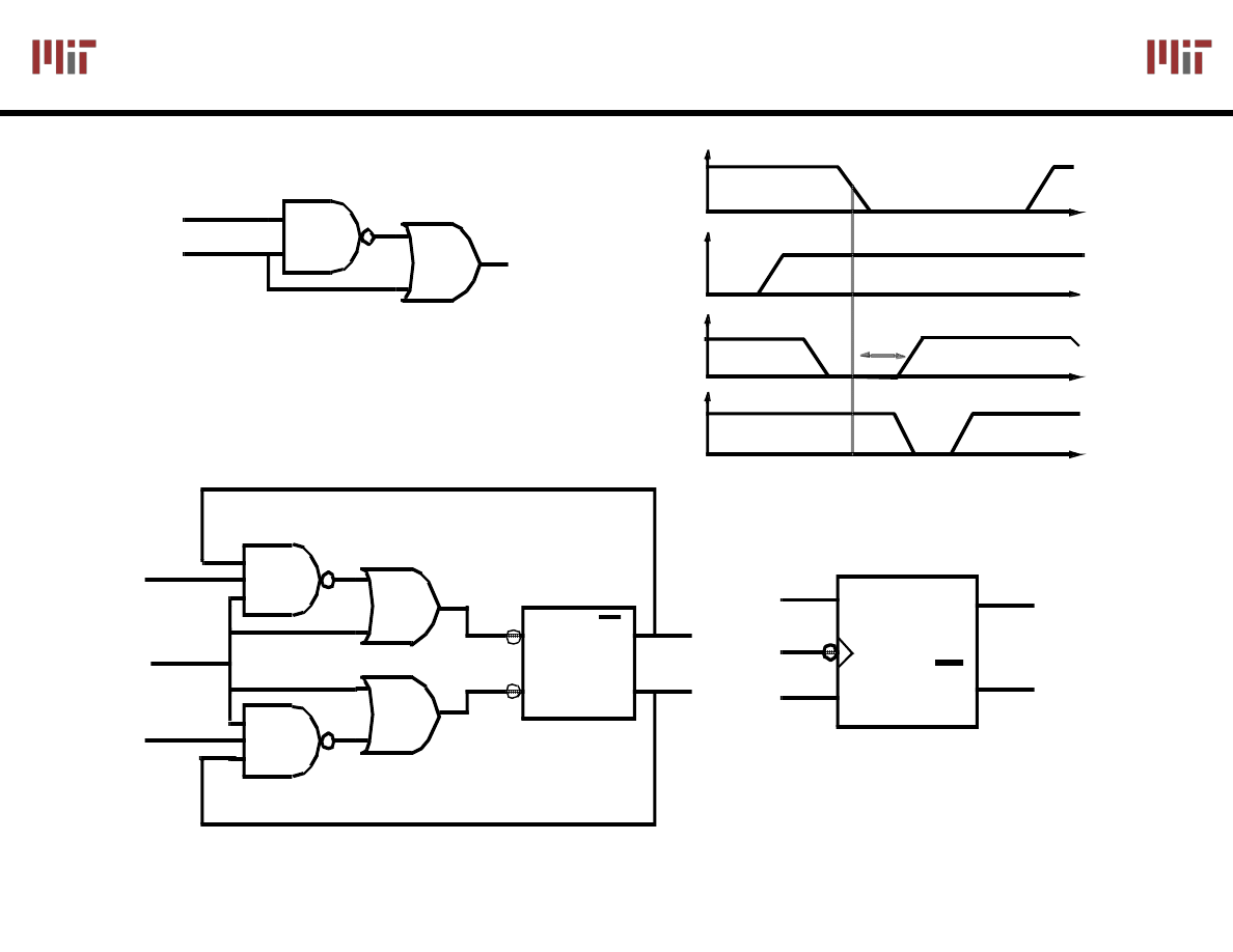
Is there a problem with this circuit?
CLK
J
K
Q
Q
φ
L4: 6.111 Spring 2006
15
Introductory Digital Systems Laboratory
Pulse Based Edge
Pulse Based Edge
-
-
Triggered J
Triggered J
-
-
K Register
K Register
S
R
Q
Q
J
K
φ
J
K
Q
Q
φ
JK Register Schematic
JK Register Logic Symbol
Input
φ
Output
Input
X
Output
t
pLH
X
φ
Schematic
L4: 6.111 Spring 2006
17
Introductory Digital Systems Laboratory
Pulse
Pulse
-
-
Triggered Registers
Triggered Registers
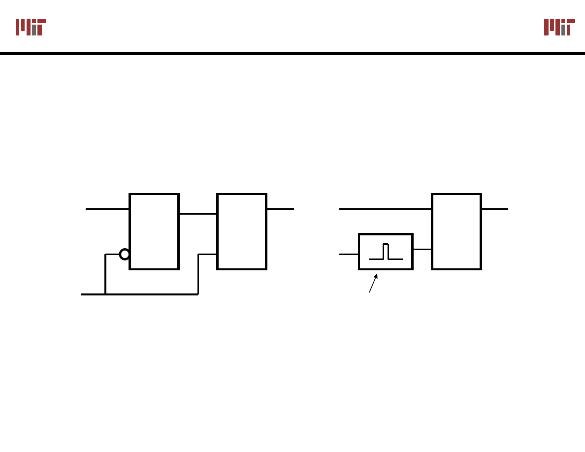
Ways to design an edge-triggered sequential cell:
Pulse-Based Register
Master-Slave Latches
D
Clk
Q
D
Clk
Q
L1
L2
Clk
Data
D
Clk
Q
Latch
Data
Clk
Short pulse around clock edge
Pulse registers are widely used in high-performance
microprocessor chips (Sun Microsystems, AMD, Intel, etc.)
The can have a negative setup time!
L4: 6.111 Spring 2006
16
Introductory Digital Systems Laboratory
D Flip
D Flip
-
-
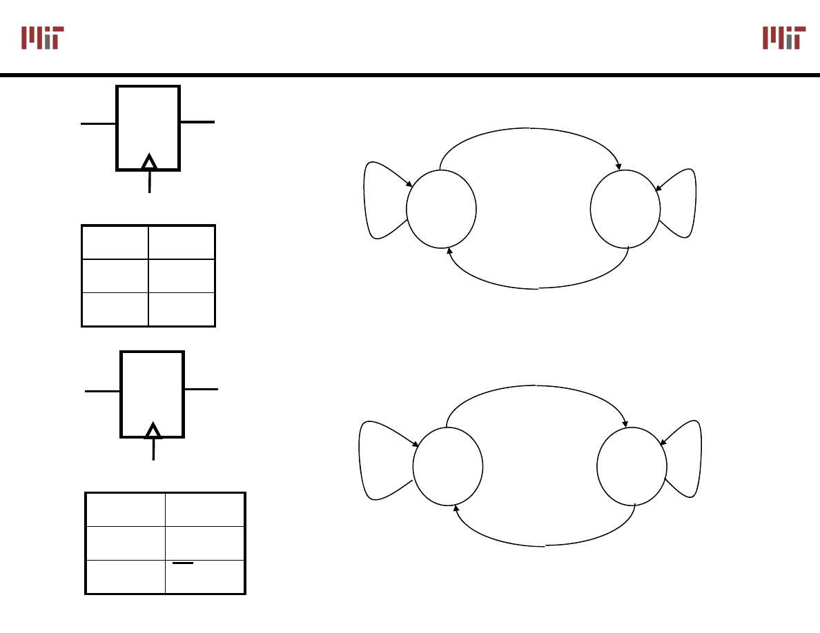
Flop vs. Toggle Flip
Flop vs. Toggle Flip
-
-
Flop
Flop
T
Clk
Q
T (Toggle)
Flip-Flop
0
1
1
1
0
T
Q
N
0
Q
N-1
1
Q
N-1
0
D
Clk
Q
D Flip-Flop
0
1
0
1
0
D
Q
N
0
0
1
1
1
L4: 6.111 Spring 2006
17
Introductory Digital Systems Laboratory
Realizing Different Types of Memory
Realizing Different Types of Memory
Elements
Elements
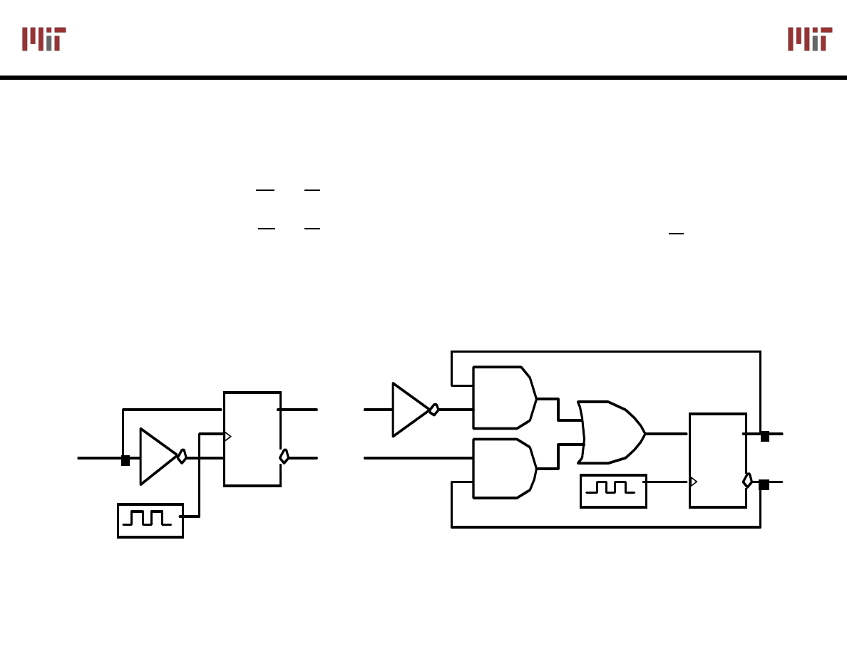
Characteristic Equations
D:
J-K:
T:
Q+ = D
Q+ = J Q + K Q
Q+ = T Q + T Q
E.g., J=K=0, then Q+ = Q
J=1, K=0, then Q+ = 1
J=0, K=1, then Q+ = 0
J=1, K=1, then Q+ = Q
Implementing One FF in Terms of Another
D implemented with J-K
J-K implemented with D
D
J
K
J
K
C
Q
Q
C
D Q
Q
Q
L4: 6.111 Spring 2006
18
Introductory Digital Systems Laboratory
Design Procedure
Design Procedure
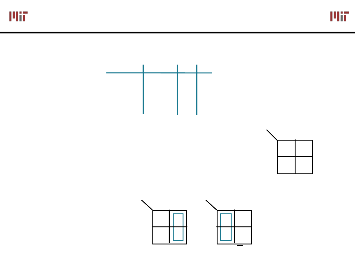
Excitation Tables: What are the necessary inputs to cause a particular kind of
change in state?
Implementing D FF with a J-K FF:
1) Start with K-map of Q+ = ƒ(D, Q)
2) Create K-maps for J and K with same inputs (D, Q)
3) Fill in K-maps with appropriate values for J and K
to cause the same state changes as in the original K-map
E.g., D = Q= 0, Q+ = 0
then J = 0, K = X
D
0 1
0 1
Q + = D
0 1
0
1
Q
D
X X
1 0
K = D
0 1
0
1
Q
D
0 1
X X
J = D
0 1
0
1
Q
D
0
1
0
1
T
0
1
1
0
Q
+
0
1
0
1
Q
0
0
1
1
K
X
X
1
0
J
0
1
X
X
L4: 6.111 Spring 2006
19
Introductory Digital Systems Laboratory
Design Procedure (cont.)
Design Procedure (cont.)
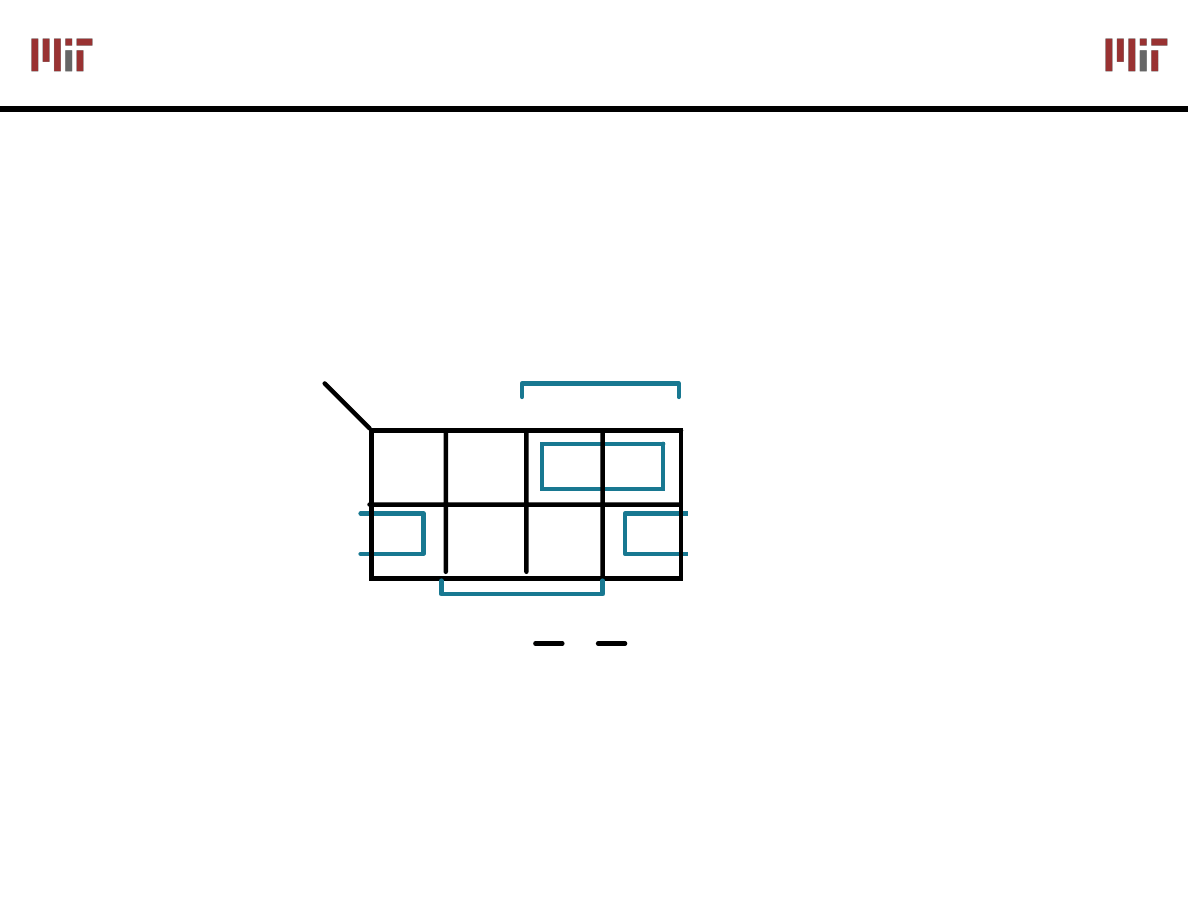
Implementing J-K FF with a D FF:
1) K-Map of Q+ = F(J, K, Q)
2,3) Revised K-map using D's excitation table
its the same! that is why design procedure with D FF is simple!
Resulting equation is the combinational logic input to D
to cause same behavior as J-K FF. Of course it is identical
to the characteristic equation for a J-K FF.
0
0 1 1
1 0 0 1
00 01 11 10
J
K
JK
Q
Q
+
= D = JQ + KQ
0
1
L4: 6.111 Spring 2006
20
Introductory Digital Systems Laboratory
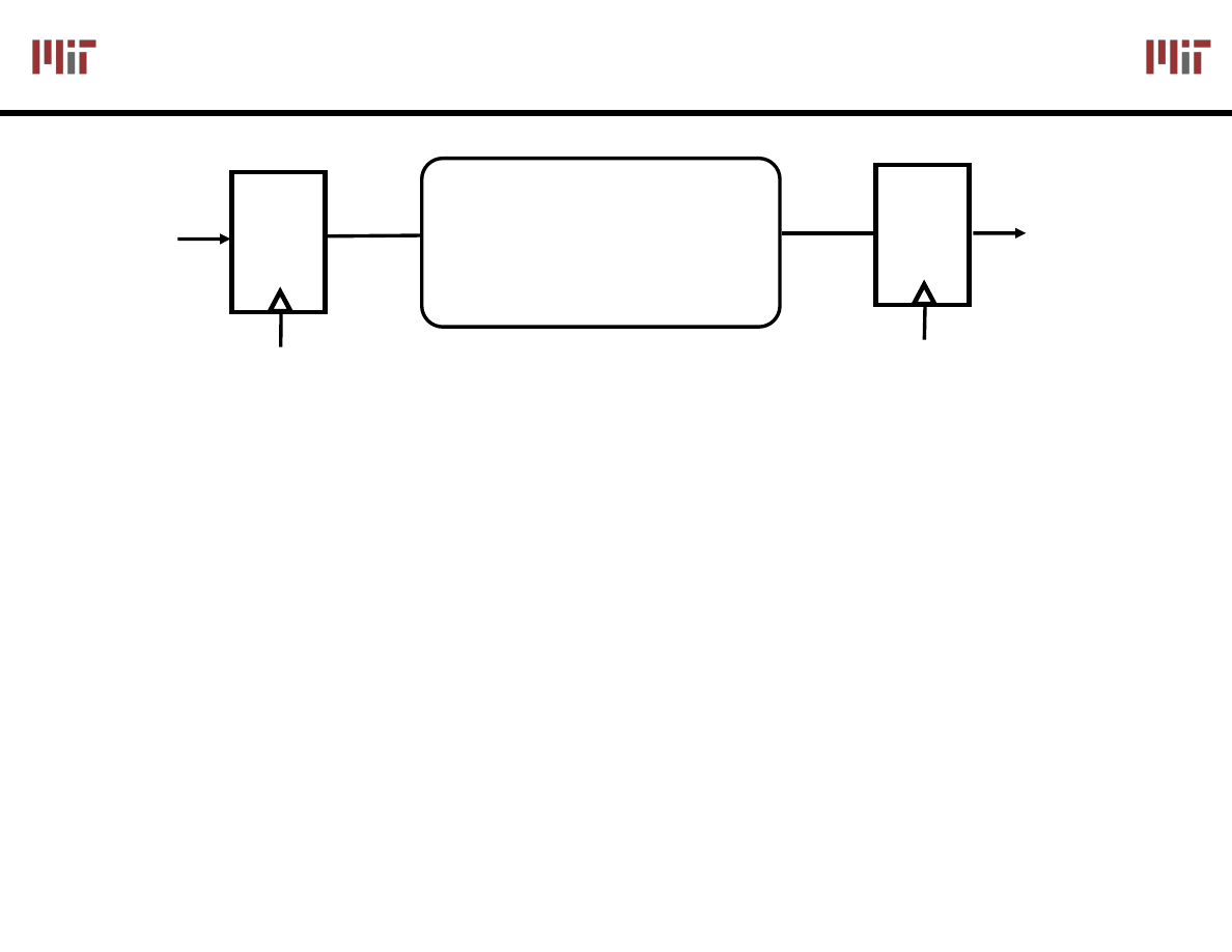
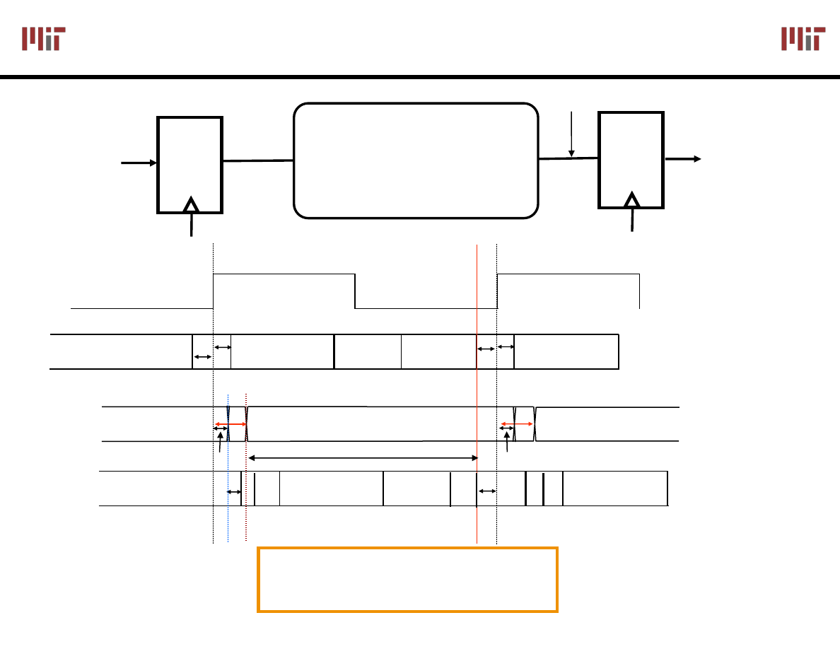
System Timing Parameters
System Timing Parameters
D
Clk
Q
In
Combinational
Logic
D
Clk
Q
Register Timing Parameters
T
cq
: worst case rising edge
clock to q delay
T
cq, cd
: contamination or
minimum delay from
clock to q
T
su
: setup time
T
h
: hold time
Logic Timing Parameters
T
logic
: worst case delay
through the combinational
logic network
T
logic,cd
: contamination or
minimum delay
through logic network
L4: 6.111 Spring 2006
21
Introductory Digital Systems Laboratory
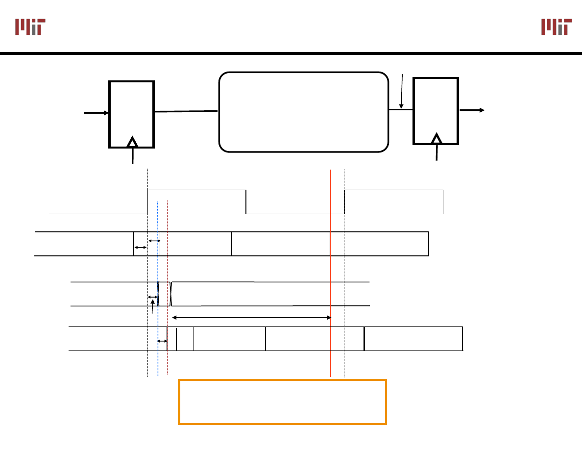
System Timing (I): Minimum Period
System Timing (I): Minimum Period
D
Clk
Q
In
Combinational
Logic
D
Clk
Q
CLK
T
su
T
h
T
su
T
h
T
cq
T
cq,cd
T
cq
T
cq,cd
FF1
IN
CLout
CLout
T
l,cd
T
su2
T
logic
T > T
cq
+ T
logic
+ T
su
L4: 6.111 Spring 2006
22
Introductory Digital Systems Laboratory
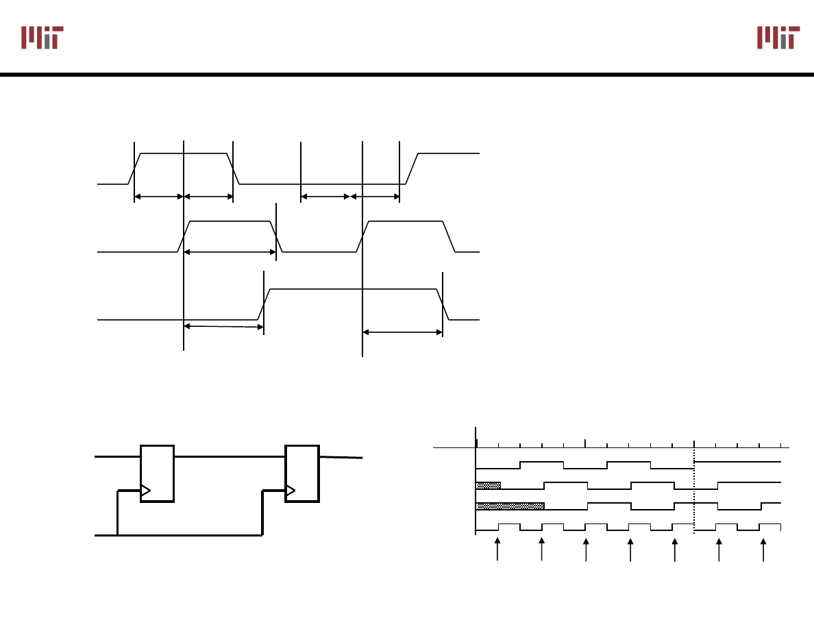
System Timing (II): Minimum Delay
System Timing (II): Minimum Delay
D
Clk
Q
In
Combinational
Logic
D
Clk
Q
CLK
T
su
T
h
T
h
T
cq,cd
FF1
IN
CLout
T
l,cd
T
cq,cd
+ T
logic,cd
> T
hold
CLout
L4: 6.111 Spring 2006
23
Introductory Digital Systems Laboratory
Shift
Shift
-
-
Register
Register
all measurements are made
from the clocking event that is,
the rising edge of the clock
Typical parameters for Positive edge-triggered D Register
Th
5ns
Tw 25ns
Tplh
25ns
13ns
Tphl
40ns
25ns
Tsu
20ns
D
CLK
Q
Tsu
20ns
Th
5ns
IN
Q0
Q1
CLK
100
CLK
IN
Q0
Q1
DQ
DQ
OUT
Shift-register
Document Outline
- L4: Sequential Building Blocks (Flip-flops, Latches and Registers)
- Combinational Logic Review
- A Sequential System
- A Simple Example
- Implementing State: Bi-stability
- NOR-based Set-Reset (SR) Flipflop
- Making a Clocked Memory Element: Positive D-Latch
- Multiplexor Based Positive & Negative Latch
- 74HC75 (Positive Latch)
- Building an Edge-Triggered Register
- Latches vs. Edge-Triggered Register
- Important Timing Parameters
- The J-K Flip-Flop
- J-K Master-Slave Register
- Pulse Based Edge-Triggered J-K Register
- D Flip-Flop vs. Toggle Flip-Flop
- Realizing Different Types of Memory Elements
- Design Procedure
- Design Procedure (cont.)
- System Timing Parameters
- System Timing (I): Minimum Period
- System Timing (II): Minimum Delay
- Shift-Register
Wyszukiwarka
Podobne podstrony:
7050 astatotilapia nubila 7 l4
7018 pyszczak moora delfinek 123 l4
L4
L4 (3)
1 LIST L4
1 3 m5 L4
L4 regresja liniowa klucz (2)
6501 zbrojnik czerwony 59 l4
L4 - pytania, Studia, Wytrzymałość materiałów II, lab4 wm2 studek
3717 zwinnik ogonopregi 188 l4
L4 5 Warstwy i napisy
l4 zbiory i funkcje wypukle
l4
FiR matma L4
7655 welon teleskop czarny 39 l4
M gr L4, PWR, PWR, 4 semestr, Grunty, Laboratorium
więcej podobnych podstron