BYV27-50, BYV27-100, BYV27-150, BYV27-200
www.vishay.com
Vishay Semiconductors
Rev. 1.8, 04-Sep-12
1
Document Number: 86042
For technical questions within your region:
DiodesAmericas@vishay.com
,
DiodesAsia@vishay.com
,
DiodesEurope@vishay.com
THIS DOCUMENT IS SUBJECT TO CHANGE WITHOUT NOTICE. THE PRODUCTS DESCRIBED HEREIN AND THIS DOCUMENT
ARE SUBJECT TO SPECIFIC DISCLAIMERS, SET FORTH AT
www.vishay.com/doc?91000
Ultra-Fast Avalanche Sinterglass Diode
MECHANICAL DATA
Case: SOD-57
Terminals: plated axial leads, solderable per MIL-STD-750,
method 2026
Polarity: color band denotes cathode end
Mounting position: any
Weight: approx. 369 mg
FEATURES
• Controlled avalanche characteristic
• Low forward voltage
• Ultra fast recovery time
• Glass passivated junction
• Hermetically sealed package
• Material categorization:
For definitions of compliance please see
www.vishay.com/doc?99912
APPLICATIONS
• Very fast rectification diode e.g. for switch mode power
supply
949539
ORDERING INFORMATION (Example)
DEVICE NAME
ORDERING CODE
TAPED UNITS
MINIMUM ORDER QUANTITY
BYV27-200
BYV27-200-TR
5000 per 10" tape and reel
25 000
BYV27-200
BYV27-200-TAP
5000 per ammopack
25 000
PARTS TABLE
PART
TYPE DIFFERENTIATION
PACKAGE
BYV27-50
V
R
= 50 V; I
F(AV)
= 2 A
SOD-57
BYV27-100
V
R
= 100 V; I
F(AV)
= 2 A
SOD-57
BYV27-150
V
R
= 150 V; I
F(AV)
= 2 A
SOD-57
BYV27-200
V
R
= 200 V; I
F(AV)
= 2 A
SOD-57
ABSOLUTE MAXIMUM RATINGS (T
amb
= 25 °C, unless otherwise specified)
PARAMETER
TEST CONDITION
PART
SYMBOL
VALUE
UNIT
Peak reverse voltage, non repetitive
See electrical characteristics
BYV27-50
V
RSM
55
V
BYV27-100
V
RSM
110
V
BYV27-150
V
RSM
165
V
BYV27-200
V
RSM
220
V
Reverse voltage = repetitive peak reverse
voltage
See electrical characteristics
BYV27-50
V
R
= V
RRM
50
V
BYV27-100
V
R
= V
RRM
100
V
BYV27-150
V
R
= V
RRM
150
V
BYV27-200
V
R
= V
RRM
200
V
Peak forward surge current
t
p
= 10 ms, half sine wave
I
FSM
50
A
Repetitive peak forward current
I
FRM
15
A
Average forward current
I
F(AV)
2
A
Pulse energy in avalanche
mode, non repetitive (inductive
load switch off)
I
(BR)R
= 1 A, T
j
= 175 °C
E
R
20
mJ
Junction and storage temperature range
T
j
= T
stg
- 55 to + 175
°C
MAXIMUM THERMAL RESISTANCE (T
amb
= 25 °C, unless otherwise specified)
PARAMETER
TEST CONDITION
SYMBOL
VALUE
UNIT
Junction ambient
l = 10 mm, T
L
= constant
R
thJA
45
K/W
On PC board with spacing 25 mm
R
thJA
100
K/W
BYV27-50, BYV27-100, BYV27-150, BYV27-200
www.vishay.com
Vishay Semiconductors
Rev. 1.8, 04-Sep-12
2
Document Number: 86042
For technical questions within your region:
DiodesAmericas@vishay.com
,
DiodesAsia@vishay.com
,
DiodesEurope@vishay.com
THIS DOCUMENT IS SUBJECT TO CHANGE WITHOUT NOTICE. THE PRODUCTS DESCRIBED HEREIN AND THIS DOCUMENT
ARE SUBJECT TO SPECIFIC DISCLAIMERS, SET FORTH AT
www.vishay.com/doc?91000
TYPICAL CHARACTERISTICS (T
amb
= 25
C, unless otherwise specified)
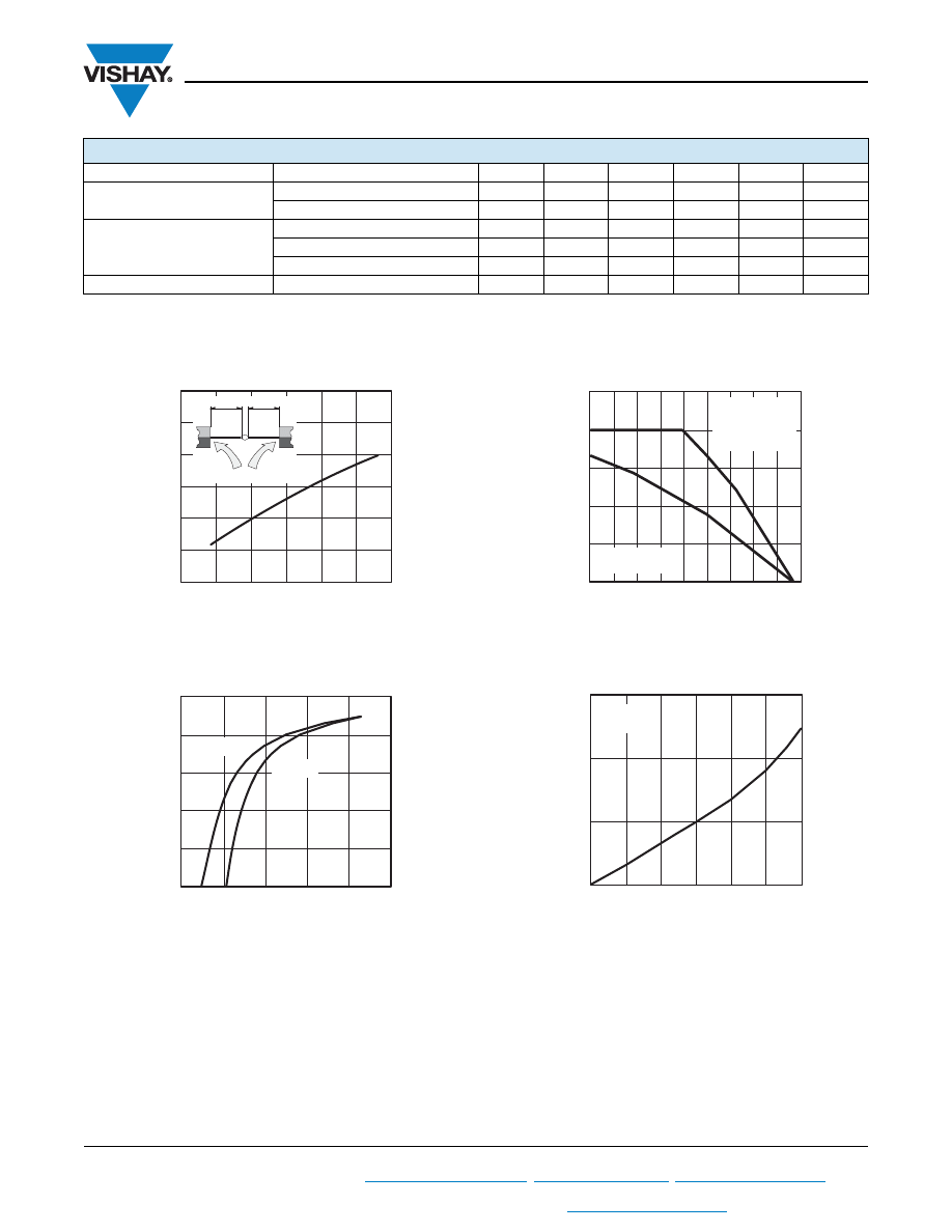
Fig. 1 - Typ. Thermal Resistance vs. Lead Length
Fig. 2 - Forward Current vs. Forward Voltage
Fig. 3 - Max. Average Forward Current vs. Ambient Temperature
Fig. 4 - Reverse Current vs. Junction Temperature
ELECTRICAL CHARACTERISTICS (T
amb
= 25 °C, unless otherwise specified)
PARAMETER
TEST CONDITION
PART
SYMBOL
MIN.
TYP.
MAX.
UNIT
Forward voltage
I
F
= 3A
V
F
-
-
1.07
V
I
F
= 3 A, T
j
= 175 °C
V
F
-
-
0.88
V
Reverse current
V
R
= V
RRM
I
R
-
-
1
μA
V
RSM
I
R
-
-
100
μA
V
R
= V
RRM
, T
j
= 165 °C
I
R
-
-
150
μA
Reverse recovery time
I
F
= 0.5 A, I
R
= 1 A, i
R
= 0.25 A
t
rr
-
-
25
ns
0
5
10
15
20
25
30
0
20
40
60
80
120
R
thJA
- Therm.Re
s
is
t.Junction/Ambient (K/W)
l - Lead Length (mm)
949526
100
l
l
T
L
= constant
I
F
- Forward Current (A)
0.001
0.01
0.1
1
10
100
0.0
0.5
1.0
1.5
2.0
2.5
V
F
- Forward Voltage (V)
16382
T
j
= 175 °C
T
j
= 25 °C
0.0
0.5
1.0
1.5
2.0
2.5
0
20
40
60
80
100 120 140 160 180
T
amb
- Ambient Temperature (°C)
16383
I
FAV
- Average Forward Current (A)
V
R
= V
RRM
half sine wave
R
thJA
= 45 K/W
l = 10 mm
R
thJA
= 100 K/W
PCB: d = 25 mm
1
10
100
1000
25
50
75
100
125
150
175
T
j
- Junction Temperature (°C)
16384
V
R
= V
RRM
I
R
- Rever
s
e Current (A)
BYV27-50, BYV27-100, BYV27-150, BYV27-200
www.vishay.com
Vishay Semiconductors
Rev. 1.8, 04-Sep-12
3
Document Number: 86042
For technical questions within your region:
DiodesAmericas@vishay.com
,
DiodesAsia@vishay.com
,
DiodesEurope@vishay.com
THIS DOCUMENT IS SUBJECT TO CHANGE WITHOUT NOTICE. THE PRODUCTS DESCRIBED HEREIN AND THIS DOCUMENT
ARE SUBJECT TO SPECIFIC DISCLAIMERS, SET FORTH AT
www.vishay.com/doc?91000
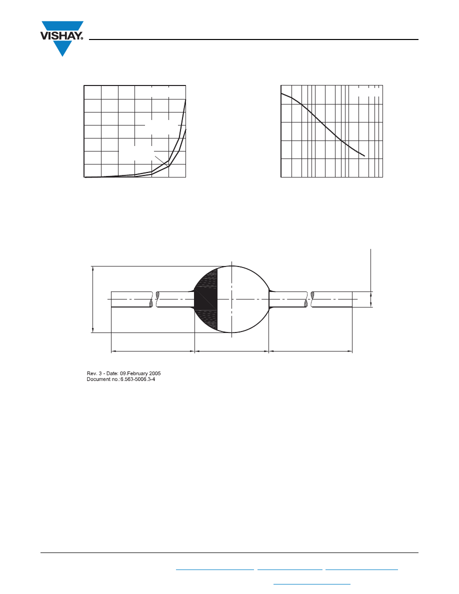
Fig. 5 - Max. Reverse Power Dissipation vs. Junction Temperature
Fig. 6 - Diode Capacitance vs. Reverse Voltage
PACKAGE DIMENSIONS in millimeters (inches): SOD-57
0
10
20
30
40
50
60
70
25
50
75
100
125
150
175
16385
P
R
- Rever
s
e Power Di
ss
ipation (mW)
T
j
- Junction Temperature (°C)
V
R
= V
RRM
P
R
- Limit
at 100 % V
R
P
R
- Limit
at 80 % V
R
0
20
40
60
80
100
0.1
1
10
100
V
R
- Reverse Voltage (V)
16386
C
D
- Diode Capacitance (pF)
f = 1 MHz
20543
3.6 (0.142) max.
26 (1.024) min.
4 (0.157) max.
26 (1.024) min.
0.82 (0.032) max.

Legal Disclaimer Notice
www.vishay.com
Vishay
Revision: 02-Oct-12
1
Document Number: 91000
Disclaimer
ALL PRODUCT, PRODUCT SPECIFICATIONS AND DATA ARE SUBJECT TO CHANGE WITHOUT NOTICE TO IMPROVE
RELIABILITY, FUNCTION OR DESIGN OR OTHERWISE.
Vishay Intertechnology, Inc., its affiliates, agents, and employees, and all persons acting on its or their behalf (collectively,
“Vishay”), disclaim any and all liability for any errors, inaccuracies or incompleteness contained in any datasheet or in any other
disclosure relating to any product.
Vishay makes no warranty, representation or guarantee regarding the suitability of the products for any particular purpose or
the continuing production of any product. To the maximum extent permitted by applicable law, Vishay disclaims (i) any and all
liability arising out of the application or use of any product, (ii) any and all liability, including without limitation special,
consequential or incidental damages, and (iii) any and all implied warranties, including warranties of fitness for particular
purpose, non-infringement and merchantability.
Statements regarding the suitability of products for certain types of applications are based on Vishay’s knowledge of typical
requirements that are often placed on Vishay products in generic applications. Such statements are not binding statements
about the suitability of products for a particular application. It is the customer’s responsibility to validate that a particular
product with the properties described in the product specification is suitable for use in a particular application. Parameters
provided in datasheets and/or specifications may vary in different applications and performance may vary over time. All
operating parameters, including typical parameters, must be validated for each customer application by the customer’s
technical experts. Product specifications do not expand or otherwise modify Vishay’s terms and conditions of purchase,
including but not limited to the warranty expressed therein.
Except as expressly indicated in writing, Vishay products are not designed for use in medical, life-saving, or life-sustaining
applications or for any other application in which the failure of the Vishay product could result in personal injury or death.
Customers using or selling Vishay products not expressly indicated for use in such applications do so at their own risk. Please
contact authorized Vishay personnel to obtain written terms and conditions regarding products designed for such applications.
No license, express or implied, by estoppel or otherwise, to any intellectual property rights is granted by this document or by
any conduct of Vishay. Product names and markings noted herein may be trademarks of their respective owners.
Material Category Policy
Vishay Intertechnology, Inc. hereby certifies that all its products that are identified as RoHS-Compliant fulfill the
definitions and restrictions defined under Directive 2011/65/EU of The European Parliament and of the Council
of June 8, 2011 on the restriction of the use of certain hazardous substances in electrical and electronic equipment
(EEE) - recast, unless otherwise specified as non-compliant.
Please note that some Vishay documentation may still make reference to RoHS Directive 2002/95/EC. We confirm that
all the products identified as being compliant to Directive 2002/95/EC conform to Directive 2011/65/EU.
Vishay Intertechnology, Inc. hereby certifies that all its products that are identified as Halogen-Free follow Halogen-Free
requirements as per JEDEC JS709A standards. Please note that some Vishay documentation may still make reference
to the IEC 61249-2-21 definition. We confirm that all the products identified as being compliant to IEC 61249-2-21
conform to JEDEC JS709A standards.
Wyszukiwarka
Podobne podstrony:
BYV27 series 50 600
200 Megapikseli w 50 megapikselowej lustrzance Hasselblada
Dane techniczne MOS 150 50, 150 65, 200 80, 250 100
200 Megapikseli w 50 megapikselowej lustrzance Hasselblada
Vishay LTO 50
(50) Środki przeczyszczająceid 1089 ppt
200 Faszyzm 2id 21545 ppt
09 1993 46 50
50 104 id 40827 Nieznany (2)
50 Common Birds An Illistrated Guide to 50 of the Most Common North American Birds
C++ 50 efektywnych sposobów na udoskonalenie Twoich programów
Perswazyjny telemarketing 50 narzedzi sprzedazy i obslugi klienta przez telefon do zastosowania od z
43 Appl Phys Lett 88 013901 200 Nieznany (2)
50 55
więcej podobnych podstron