
DOE-HDBK-1016/2-93
JANUARY 1993
DOE FUNDAMENTALS HANDBOOK
ENGINEERING SYMBOLOGY,
PRINTS, AND DRAWINGS
Volume 2 of 2
U.S. Department of Energy
FSC-6910
Washington, D.C. 20585
Distribution Statement A. Approved for public release; distribution is unlimited.

This document has been reproduced directly from the best available copy.
Available to DOE and DOE contractors from the Office of Scientific and
Technical Information, P.O. Box 62, Oak Ridge, TN 37831.
Available to the public from the National Technical Information Services, U.S.
Department of Commerce, 5285 Port Royal., Springfield, VA 22161.
Order No. DE93012181

DOE-HDBK-1016/2-93
ENGINEERING SYMBOLOGY, PRINTS, AND DRAWINGS
ABSTRACT
The
Engineering S ym bology, Prints, and Draw ings
Handbook was developed to assist
nuclear facility operating contractors in providing operators, maintenance personnel, and technical
staff with the necessary fundamentals training to ensure a basic understanding of engineering
prints, their use, and their function. The handbook includes information on engineering fluid
drawings and prints; piping and instrument drawings; major symbols and conventions; electronic
diagrams and schematics; logic circuits and diagrams; and fabrication, construction, and
architectural drawings. This information will provide personnel with a foundation for reading,
interpreting, and using the engineering prints and drawings that are associated with various DOE
nuclear facility operations and maintenance.
Key Words:
Training Material, Print Reading, Piping and Instrument Drawings, Schematics,
Electrical Diagrams, Block Diagrams, Logic Diagrams, Fabrication Drawings, Construction
Drawings, Architectural Drawings
Rev. 0
PR


DOE-HDBK-1016/2-93
ENGINEERING SYMBOLOGY, PRINTS, AND DRAWINGS
FOREWORD
The
Departm ent of Energy (DOE) Fundam entals Handbooks
consist of ten academic
subjects, which include Mathematics; Classical Physics; Thermodynamics, Heat Transfer, and
Fluid Flow; Instrumentation and Control; Electrical Science; Material Science; Mechanical
Science; Chemistry; Engineering Symbology, Prints, and Drawings; and Nuclear Physics and
Reactor Theory. The handbooks are provided as an aid to DOE nuclear facility contractors.
These handbooks were first published as Reactor Operator Fundamentals Manuals in 1985
for use by DOE category A reactors. The subject areas, subject matter content, and level of
detail of the Reactor Operator Fundamentals Manuals were determined from several sources.
DOE Category A reactor training managers determined which materials should be included, and
served as a primary reference in the initial development phase. Training guidelines from the
commercial nuclear power industry, results of job and task analyses, and independent input from
contractors and operations-oriented personnel were all considered and included to some degree
in developing the text material and learning objectives.
The
DOE Fundam entals Handbooks
represent the needs of various DOE nuclear facilities'
fundamental training requirements. To increase their applicability to nonreactor nuclear facilities,
the Reactor Operator Fundamentals Manual learning objectives were distributed to the Nuclear
Facility Training Coordination Program Steering Committee for review and comment. To update
their reactor-specific content, DOE Category A reactor training managers also reviewed and
commented on the content. On the basis of feedback from these sources, information that applied
to two or more DOE nuclear facilities was considered generic and was included. The final draft
of each of the handbooks was then reviewed by these two groups. This approach has resulted
in revised modular handbooks that contain sufficient detail such that each facility may adjust the
content to fit their specific needs.
Each handbook contains an abstract, a foreword, an overview, learning objectives, and text
material, and is divided into modules so that content and order may be modified by individual
DOE contractors to suit their specific training needs. Each handbook is supported by a separate
examination bank with an answer key.
The
DOE Fundam entals Handbooks
have been prepared for the Assistant Secretary for
Nuclear Energy, Office of Nuclear Safety Policy and Standards, by the DOE Training
Coordination Program. This program is managed by EG&G Idaho, Inc.
Rev. 0
PR


DOE-HDBK-1016/2-93
ENGINEERING SYMBOLOGY, PRINTS, AND DRAWINGS
OVERVIEW
The
Departm ent of Energy Fundam entals Handbook
entitled
Engineering S ym bology,
Prints, and Draw ings
was prepared as an information resource for personnel who are responsible
for the operation of the Department's nuclear facilities. A basic understanding of engineering
prints and drawings is necessary for DOE nuclear facility operators, maintenance personnel, and
the technical staff to safely operate and maintain the facility and facility support systems. The
information in the handbook is presented to provide a foundation for applying engineering
concepts to the job. This knowledge will improve personnel understanding of the impact that
their actions may have on the safe and reliable operation of facility components and systems.
The
Engineering Sym bology, Prints, and Draw ings
handbook consists of six modules that
are contained in two volumes. The following is a brief description of the information presented
in each module of the handbook.
Module 1 - Introduction to Print Reading
This module introduces each type of drawing and its various formats. It also
reviews the information contained in the non-drawing areas of a drawing.
Module 2 - Engineering Fluid Diagrams and Prints
This module introduces engineering fluid diagrams and prints (P&IDs); reviews
the common symbols and conventions used on P&IDs; and provides several
examples of how to read a P&ID.
Module 3 - Electrical Diagrams and Schematics
This module reviews the major symbols and conventions used on electrical
schematics and single line drawings and provides several examples of reading
electrical prints.
Rev. 0
PR


DOE-HDBK-1016/2-93
ENGINEERING SYMBOLOGY, PRINTS, AND DRAWINGS
OVERVIEW (Cont.)
Volume 2 of 2
Module 4 - Electronic Diagrams and Schematics
This module reviews electronic schematics and block diagrams. It covers the
major symbols used and provides several examples of reading these types of
drawings.
This module introduces the basic symbols and common conventions used on logic
diagrams. It explains how logic prints are used to represent a component's control
circuits. Truth tables are also briefly discusses and several examples of reading
logic diagrams are provided.
Module 6 - Engineering Fabrication, Construction, and Architectural Drawings
This module reviews fabrication, construction, and architectural drawings and
introduces the symbols and conventions used to dimension and tolerance these
types of drawings.
The information contained in this handbook is by no means all encompassing. An attempt
to present the entire subject of engineering drawings would be impractical. However, the
Engineering S ym bology, Prints, and Draw ings
handbook does present enough information to
provide the reader with a fundamental knowledge level sufficient to understand the advanced
theoretical concepts presented in other subject areas, and to improve understanding of basic
system operation and equipment operations.
Rev. 0
PR


Electronic Diagrams and Schematics
DOE-HDBK-1016/2-93
TABLE OF CONTENTS
TABLE OF CONTENTS
ELECTRONIC DIAGRAMS AND SCHEMATICS
Introduction
Electronic Schematic Drawing Symbology
Examples of Electronic Schematic Diagrams
Reading Electronic Prints, Diagrams, and Schematics
Block Drawing Symbology
Examples of Block Diagrams
Summary
Rev. 0
Page i
P R - 0 4

LIST OF FIGURES
DOE-HDBK-1016/2-93
Electronic Diagrams and Schematics
Figure
Figure
Figure
Figure
Figure
Figure
Figure
Figure
Figure
Figure
Figure
Figure
Figure
Figure
Figure
Figure
Figure
1
2
3
4
5
6
7
8
9
10
11
1 2
1 3
14
1 5
1 6
1 7
Electronic Symbols
Electronic Symbols (Continued)
Example of an Electronic Schematic Diagram
Comparison of an Electronic Schematic Diagram
and its Pictorial Layout Diagram
Transformer Polarity Markings
Schematic Showing Power Supply Connections
NPN Transistor-Conducting
NPN Transistor-Nonconducting
PNP Transistor
Diode
Bistable Symbols
Example Blocks
Example Block Diagram
Example of a Combined Drawing, P&ID, Electrical Single Line,
and Electronic Block Diagram
.
Combination
Example
Example
Example
Diagram of Electrical Single Line, and Block Diagram
1
2
PR-04
Page ii
Rev. 0

Electronic Diagrams and Schematics
DOE-HDBK-1016/2-93
LIST OF TABLES
NONE
Rev. 0
Page iii
P R - 0 4
REFERENCES
DOE-HDBK-1016/2-93
Electronic Diagrams and Schematics
ANSI Y14.5M - 1982, Dimensioning and Tolerancing, American National Standards
Institute.
ANSI Y32.2 -1975, Graphic Symbols for Electrical and Electronic Diagrams, American
National Standards Institute.
Gasperini, Richard E., Digital Troubleshooting, Movonics Company; Los Altos,
California, 1976.
Jensen - Helsel, Engineering Drawing and Design, Second Ed., McGraw-Hill Book
Company, New York, 1979.
Lenk, John D., Handbook of Logic Circuits, Reston Publishing Company, Reston,
Virginia, 1972.
Wickes, William E., Logic Design with Integrated Circuits, John Wiley & Sons Inc,
1968.
Naval Auxiliary Machinery, United States Naval Institute, Annapolis, Maryland, 1951.
TPC Training Systems,
Reading Schematics and Symbols, Technical Publishing
Company, Barrington, Illinois, 1974.
Arnell, Alvin, Standard Graphica1 Symbols, McGraw-Hill Book Company, 1963.
George Mashe, Systems Summary of a Westinghouse Pressurized Water Reactor,
Westinghouse Electric Corporation, 1971.
Zappe, R. W., Valve Selection Handbook, Gulf Publishing Company, Houston, Texas,
1968.
.
PR-04
Page iv
Rev. 0

Electronic Diagrams and Schematics
DOE-HDBK-1016/2-93
OBJECTIVES
a.
p.
q.
g.
j.
y.
aa.
.
1.0
Given a block diagram, print, or schematic, IDENTIFY the basic component symbols
as presented in this module.
1.1
IDENTIFY the symbols used on engineering electronic block diagrams, prints, and
schematics, for the following components.
b.
c.
d.
e.
f.
h .
i .
k.
1.
m.
n.
Fixed resistor
Variable resistor
Tapped resistor
Fixed capacitor
Variable capacitor
Fixed inductor
Variable inductor
Diode
Light emitting diode (LED)
Ammeter
Voltmeter
Wattmeter
Chassis ground
Circuit ground
o.
r.
s .
t .
u.
v.
w.
x.
z.
bb.
Fuse
Plug
Headset
Light bulb
Silicon controlled rectifier (SCR)
Half wave rectifier
Full wave rectifier
Oscillator
Potentiometer
Rheostat
Antenna
Amplifier
PNP and NPN transistors
Junction
1.2
STATE the purpose of a block diagram and an electronic schematic diagram.
Rev. 0
Page v
PR-04
.
.

DOE-HDBK-1016/2-93
Electronic Diagrams and Schematics
Intentionally Left Blank.
PR-04
Page vi
Rev. 0

DOE-HDBK-1016/2-93
Electronic Diagrams and Schematics
ELECTRONIC DIAGRAMS, PRINTS, AND SCHEMATICS
Rev. 0
Page 1
PR-04
To read and understand an electronic diagram or electronic schematic,
the basic symbols and conventions must be understood.
EO 1.1
IDENTIFY the symbols used on engineering
electronic block diagrams, prints, and schematics, for
the following components.
a.
Fixed resistor
n.
Circuit ground
b.
Variable
o.
Fuse
resistor
p.
Plug
c.
Tapped resistor
q.
Headset
d.
Fixed capacitor
r.
Light bulb
e.
Variable
s.
Silicon controlled rectifier
capacitor
(SCR)
f.
Fixed inductor
t.
Half wave bridge rectifier
g.
Variable
u.
Full wave rectifier
inductor
v.
Oscillator
h.
Diode
w.
Potentiometer
i.
Light emitting
x.
Rheostat
diode (LED)
y.
Antenna
j.
Ammeter
z.
Amplifier
k.
Voltmeter
aa.
PNP and NPN transistors
l.
Wattmeter
bb.
Junction
m. Chassis ground
EO 1.2
STATE the purpose of a block diagram and an
electronic schematic diagram.
Electronic prints fall into two basic categories, electronic schematics and block diagrams.
Electronic schematics represent the most detailed category of electronic drawings. They depict
every component in a circuit, the component's technical information (such as its ratings), and
how each component is wired into the circuit. Block diagrams are the simplest type of drawing.
As the name implies, block diagrams represent any part, component, or system as a simple
geometric shape, with each block capable of representing a single component (such as a relay)
or an entire system. The intended use of the drawing dictates the level of detail provided by

DOE-HDBK-1016/2-93
ELECTRONIC DIAGRAMS, PRINTS, AND SCHEMATICS
Electronic Diagrams and Schematics
PR-04
Page 2
Rev. 0
each block. This chapter will review the basic symbols and conventions used in both types of
drawings.
Electronic Schematic Drawing Symbology
Of all the different types of electronic drawings, electronic schematics provide the most detail
and information about a circuit. Each electronic component in a given circuit will be depicted
and in most cases its rating or other applicable component information will be provided. This
type of drawing provides the level of information needed to troubleshoot electronic circuits.
Electronic schematics are the most difficult type of drawing to read, because they require a very
high level of knowledge as to how each of the electronic components affects, or is affected by,
an electrical current. This chapter reviews only the symbols commonly used in depicting the
many components in electronic systems. Once mastered, this knowledge should enable the
reader to obtain a functional understanding of most electronic prints and schematics.
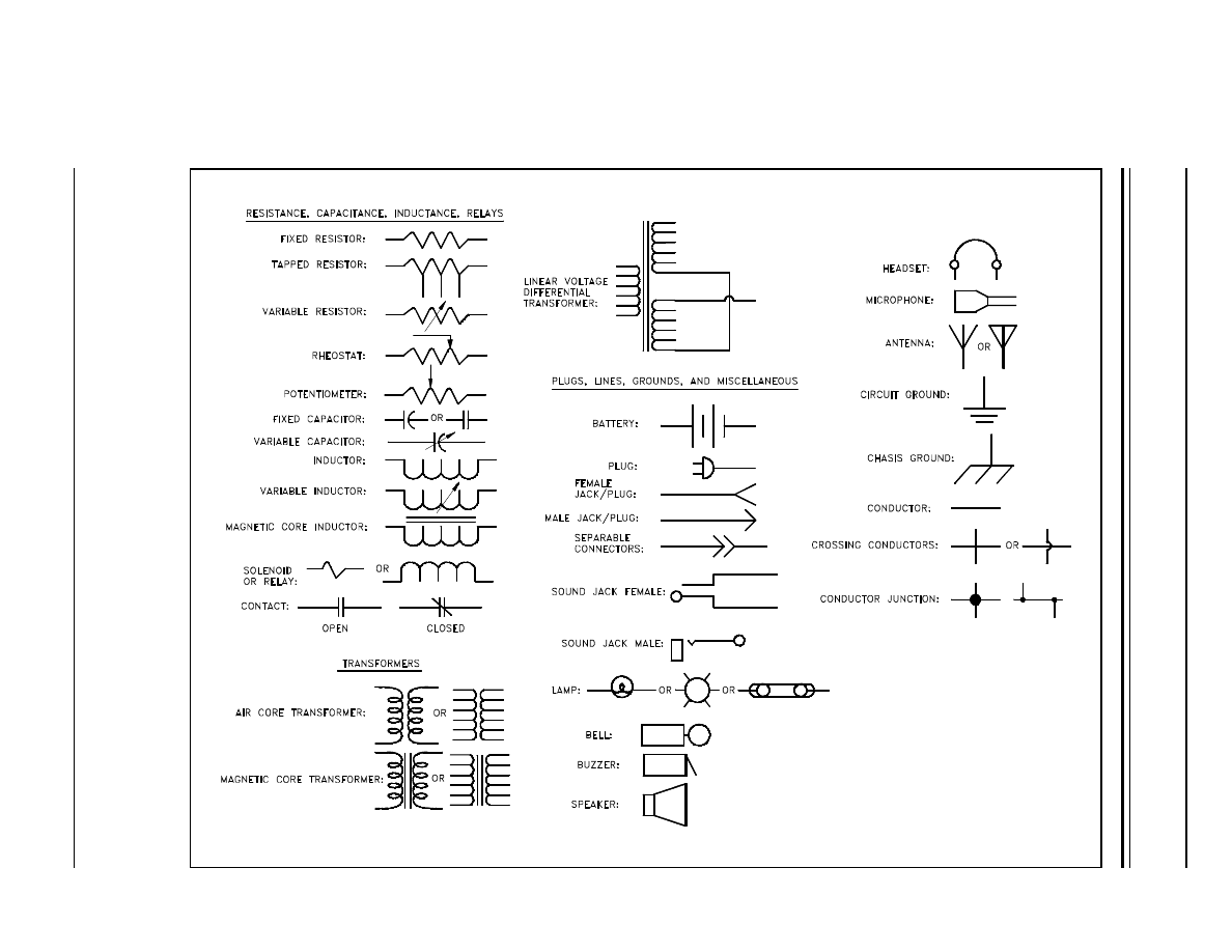
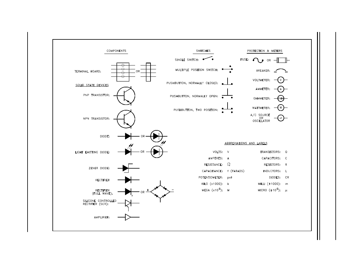
Figure 1 and Figure 2 illustrate the most common electronic symbols used on electronic
schematics.
DOE-HDBK-1016/2-93
Electronic Diagrams and Schematics
ELECTRONIC DIAGRAMS, PRINTS, AND SCHEMATICS
Rev. 0
Page 3
PR-04
DOE-HDBK-1016/2-93
ELECTRONIC DIAGRAMS, PRINTS, AND SCHEMATICS
Electronic Diagrams and Schematics
PR-04
Page 4
Rev. 0
DOE-HDBK-1016/2-93
Electronic Diagrams and Schematics
ELECTRONIC DIAGRAMS, PRINTS, AND SCHEMATICS
Rev. 0
Page 5
PR-04
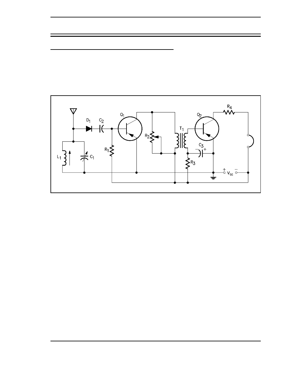
Figure 3 Example of an Electronic Schematic Diagram
Examples of Electronic Schematic Diagrams
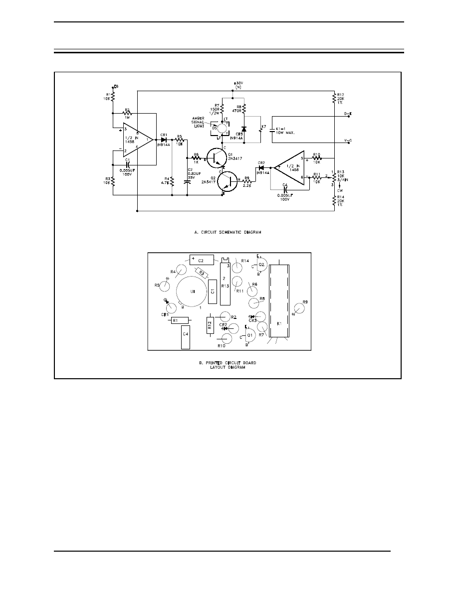
Electronic schematics use symbols for each component found in an electrical circuit, no matter
how small. The schematics do not show placement or scale, merely function and flow. From this,
the actual workings of a piece of electronic equipment can be determined. Figure 3 is an example
of an electronic schematic diagram.
A second type of electronic schematic diagram, the pictorial layout diagram, is actually not so
much an electronic schematic as a pictorial of how the electronic circuit actually looks. These
drawings show the actual layout of the components on the circuit board. This provides a
two-dimensional drawing, usually looking down from the top, detailing the components in their
location. Shown in Figure 4 is the schematic for a circuit and the same circuit drawn in pictorial
or layout format for comparison. Normally the pictorial layout would be accompanied by a parts
list.
DOE-HDBK-1016/2-93
ELECTRONIC DIAGRAMS, PRINTS, AND SCHEMATICS
Electronic Diagrams and Schematics
PR-04
Page 6
Rev. 0
Figure 4 Comparison of an Electronic Schematic Diagram and its Pictorial Layout Diagram
SECONDARY
PRIMARY
DOE-HDBK-1016/2-93
Electronic Diagrams and Schematics
ELECTRONIC DIAGRAMS, PRINTS, AND SCHEMATICS
Rev. 0
Page 7
PR-04
Figure 5 Transformer Polarity Markings
Reading Electronic Prints, Diagrams and Schematics
To properly read prints and schematics, the reader must identify the condition of the components
shown and also follow the events that occur as the circuit functions. As with electrical systems,
the relays and contacts shown are always in the de-energized condition. Modern electronic
systems usually contain few, if any, relays or contacts, so these will normally play a minor role.
Electronic schematics are more difficult to read than electrical schematics, especially when solid
state devices are used (The Electronic Science Fundamental Handbook discusses electrical
schematics in detail). Knowledge of the workings of these devices is necessary to determine
current flow. In this section, only the basics will be covered to assist in reading skills.
The first observation in dealing with a detailed electronic schematic is the source and polarity of
power. Generally, power will be shown one of two ways, either as an input transformer, or as
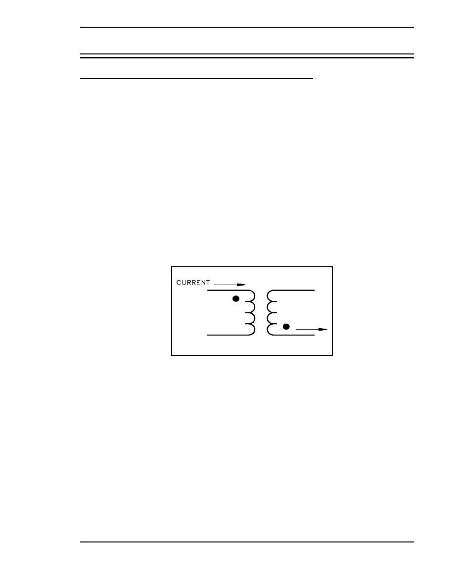
a numerical value. When power is supplied by a transformer, polarity marks will aid in
determining current flow. In this convention, dots on the primary and secondary indicate current
flow into the primary and out of the secondary at a given instant of time. In Figure 5, the current
is into the top of the primary and out of the bottom of the secondary.
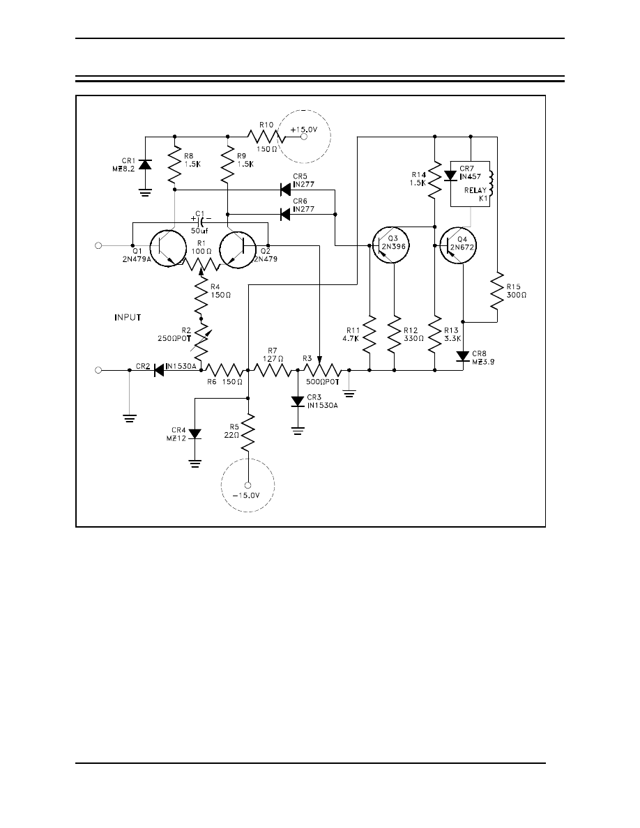
Generally, the electrical power source is indicated at the point where it enters a particular
schematic. These values are stated numerically with polarity assigned (+15 volts, -15 volts).
These markings are usually at the top and bottom of schematics, but not always. In the example
shown in Figure 6, power is shown at both the top and bottom in a circuit using two power
sources. Unless specified as an Alternating Current (AC) power source, the voltages can
normally be assumed to be Direct Current (DC).
DOE-HDBK-1016/2-93
ELECTRONIC DIAGRAMS, PRINTS, AND SCHEMATICS
Electronic Diagrams and Schematics
PR-04
Page 8
Rev. 0
Figure 6 Schematic Showing Power Supply Connections
In any circuit, a ground must be established to create a complete current path. Ground is usually
depicted by the use of the ground symbol that was shown previously. The direction of current
flow can be determined by observing the polarity of the power supplies. When polarities are
shown, current flow can be established and ground may not always be shown.
With the power sources located and the ground point established, operation of the devices can
be determined.
The most common semiconductor devices are the transistor and the diode. They are made from
materials like silicone and germanium, and have electrical properties intermediate between
conductors and insulators. The semiconductor will be one of two varieties, the PNP or NPN.
The designation indicates the direction the electrons move through the device. The direction of
DOE-HDBK-1016/2-93
Electronic Diagrams and Schematics
ELECTRONIC DIAGRAMS, PRINTS, AND SCHEMATICS
Rev. 0
Page 9
PR-04
Figure 7 NPN Transistor-Conducting
Figure 8 NPN Transistor-Nonconducting
the arrow indicates type, as shown in Figure 2. There are, however, many different ways to install
a transistor to achieve different operational characteristics. These are too numerous to cover here,
so only the most common and basic configuration (the common emitter) will be shown.
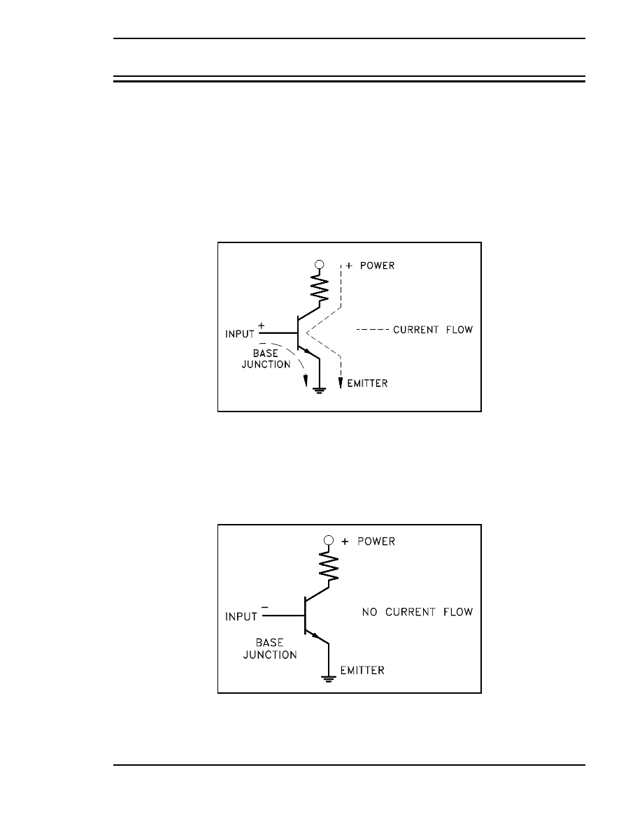
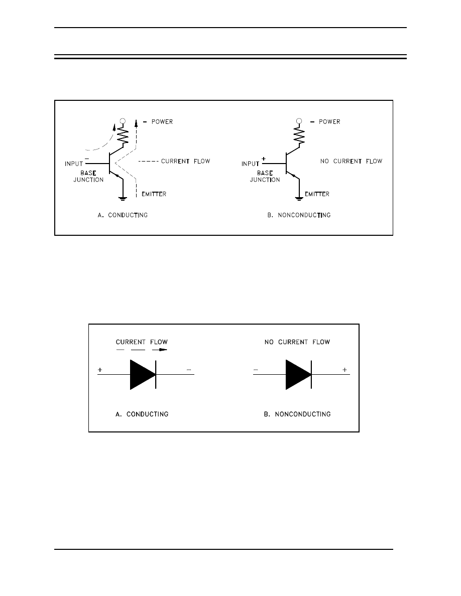
Even though transistors contain multiple junctions of p- or n-type material, current flow is
generally in the same direction. Using conventional current flow (i.e. from + to -), current will
travel through the transistor from most positive to least positive and in the direction of the arrow
on the emitter. In Figure 7, the transistor has a positive power supply with ground on the emitter.
If the input is also positive, the transistor will conduct.
If the input goes negative, as in Figure 8, the conduction of the device stops because the input,
or in this case the base junction, controls the transistor condition. Notice that when current flows,
it does so in the direction of the arrow.
DOE-HDBK-1016/2-93
ELECTRONIC DIAGRAMS, PRINTS, AND SCHEMATICS
Electronic Diagrams and Schematics
PR-04
Page 10
Rev. 0
Figure 9 uses a PNP transistor. The same rules apply as above except that this time polarities of
power must change to allow current flow.
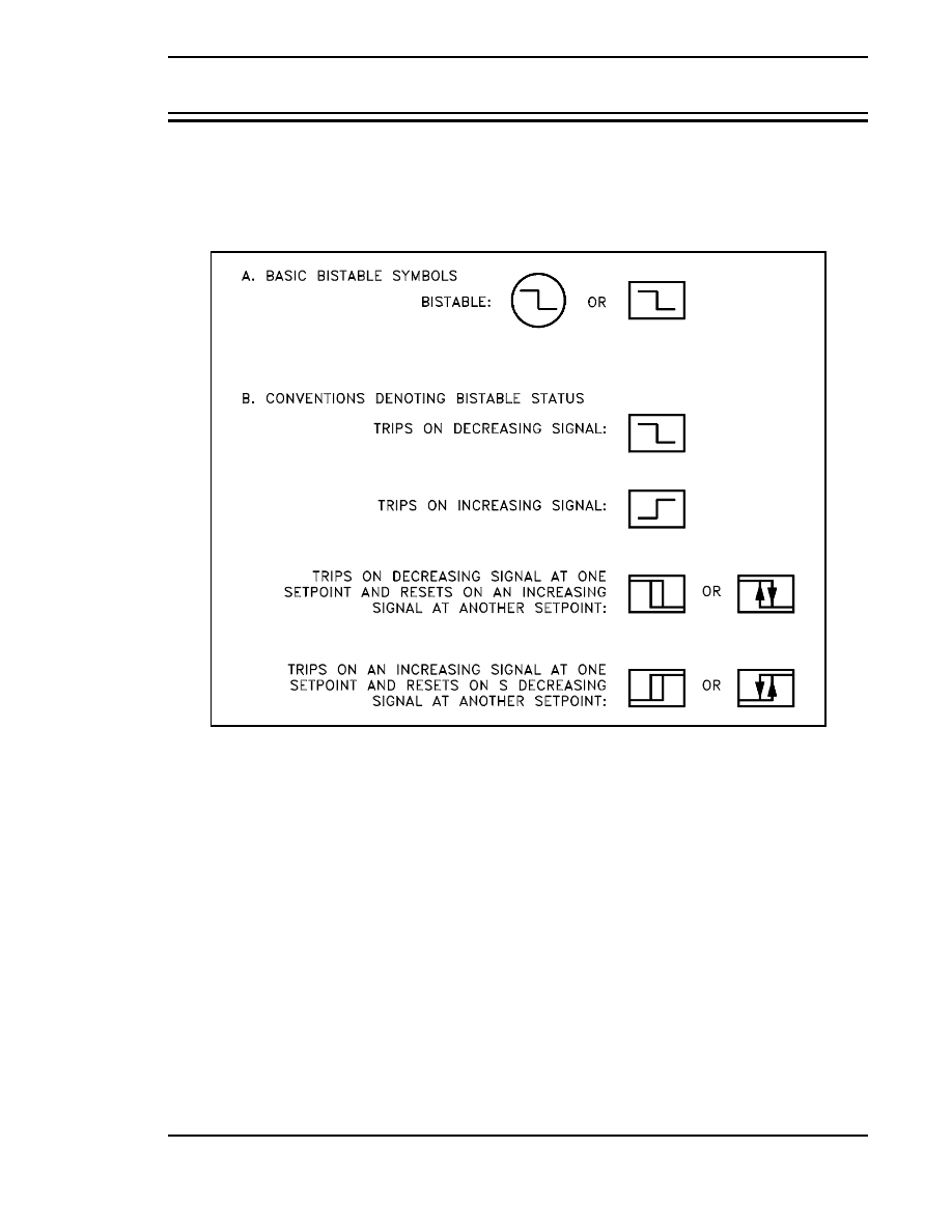
The same rules that apply to transistors hold true with diodes. However, diodes are simpler than
transistors because they have only one junction and conduct in only one direction, as indicated
in Figure 10. The diode symbol, like the transistor symbol, shows the direction of conduction by
the direction of the arrow, which is from positive to negative.
Although these simple rules will not allow you to read all electronic schematics, they will aid in
understanding some of the basic concepts.
DOE-HDBK-1016/2-93
Electronic Diagrams and Schematics
ELECTRONIC DIAGRAMS, PRINTS, AND SCHEMATICS
Rev. 0
Page 11
PR-04
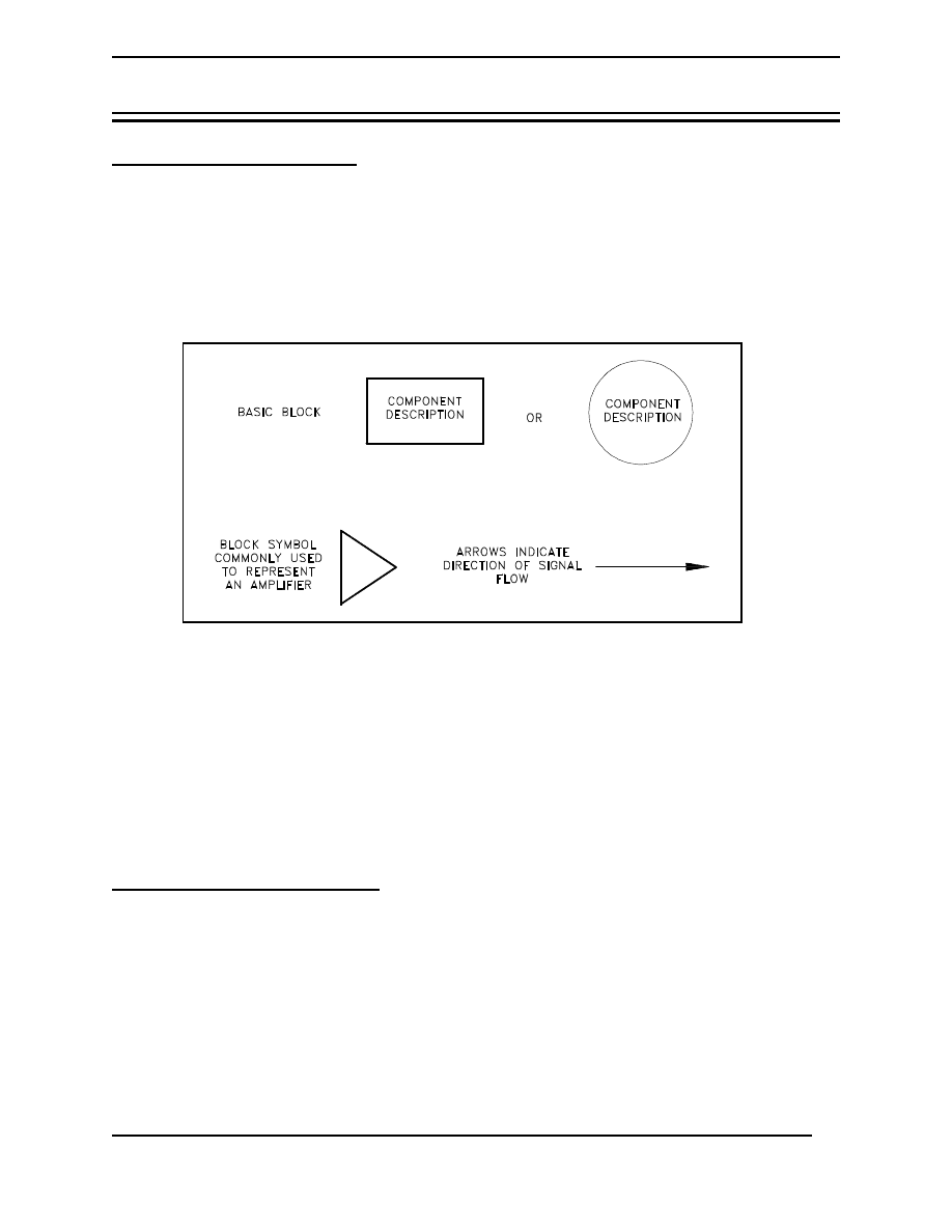
An item that may cause confusion when reading electronic prints or schematics is the markings
used to show bistable operation. In most cases, bistables will be indicated by a box or circle, as
shown in Figure 11 (A). The lines in or around these bistables not only mark them as bistables,
but also indicate how they function.
Figure 11 (B) shows the various conventions used to indicate bistable operation. Commonly,
one circuit will interface with other circuits, which requires a method that allows the reader to
follow one wire or signal path from the first drawing to the second. This may be done in many
ways, but generally the line or conductor to be continued will end at a terminal board. This
board will be labeled and numbered with the continuation drawing indicated (a separate drawing
may exist for each line). With the next drawing in hand, only the terminal board that matches
the previous number needs to be found to continue. In cases where terminal boards are not
used, the conductor should end with a number (usually a single digit) and also the next drawing
number. To assist in locating the continuation, coordinates are provided on some drawings that
indicate the location of the continuation on the second drawing. The continuation point on the
second drawing will also reference back to the first drawing and the coordinates of the
continuation.
DOE-HDBK-1016/2-93
ELECTRONIC DIAGRAMS, PRINTS, AND SCHEMATICS
Electronic Diagrams and Schematics
PR-04
Page 12
Rev. 0
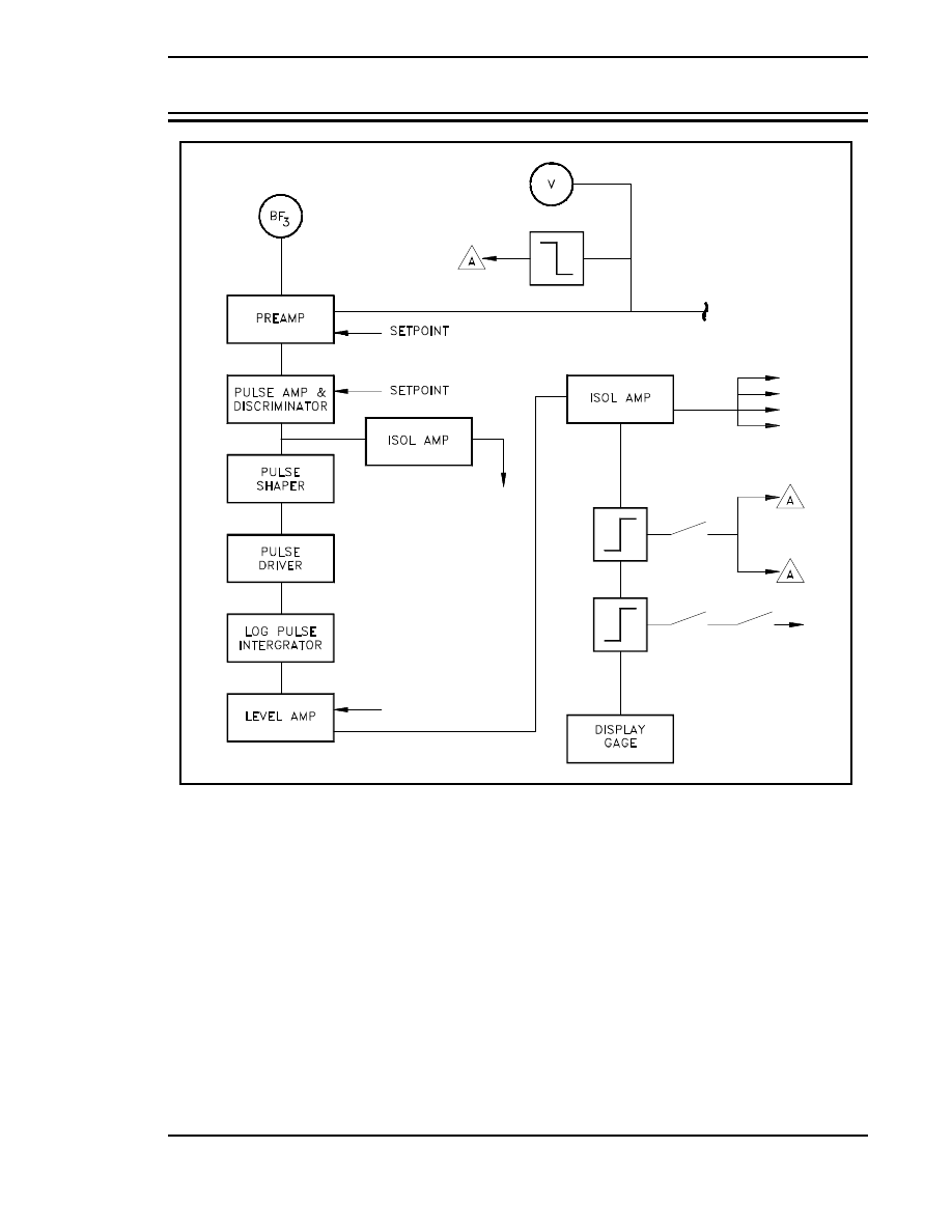
Not all electronics prints are drawn to the level of detail depicting the individual resistors and
capacitors, nor is this level of information always necessary. These simpler drawings are called
block diagrams. Block diagrams provide a means of representing any type of electronic circuit
or system in a simple graphic format. Block diagrams are designed to present flow or functional
information about the circuit or system, not detailed component data. The symbols shown in
Figure 12 are used in block diagrams.
When block diagrams are used, the basic blocks shown above (Figure 12) can be used for
almost anything. Whatever the block represents will be written inside. Note that block
diagrams are presented in this chapter with electronic schematics because block diagrams are
commonly found with complex schematic diagrams to help present or summarize their flow or
functional information. The use of block diagrams is not restricted to electronic circuits. Block
diagrams are used extensively to show complex instrument channels and other complex systems
when only the flowpath of the signal is important.
The block diagram is the most basic and easiest to understand of all the types of engineering
prints. It consists of simple blocks that can represent as much, or as little, as desired. An
example of a block diagram is shown in Figure 13.
This particular block diagram represents an instrumentation channel used to measure the
neutron flux, indicate the measured flux, and generate output signals for use by other systems.
DOE-HDBK-1016/2-93
Electronic Diagrams and Schematics
ELECTRONIC DIAGRAMS, PRINTS, AND SCHEMATICS
Rev. 0
Page 13
PR-04
Figure 13 Example Block Diagram
Each block represents a stage in the development of a signal that is used to display on the meter
at the bottom or to send to systems outside the bounds of the drawing. Notice that not all blocks
are equal. Some represent multiple functions, while others represent only a simple stage or single
bistable circuit in a larger component. The creator of the block diagram decides the content of
each block based on the intended use of the drawing.
Each of the type of drawing reviewed in this and previous modules is not always distinct and
separate. In many cases, two or more types of drawings will be combined into a single print.
This allows the necessary information to be presented in a clear and concise format.

DOE-HDBK-1016/2-93
ELECTRONIC DIAGRAMS, PRINTS, AND SCHEMATICS
Electronic Diagrams and Schematics
PR-04
Page 14
Rev. 0
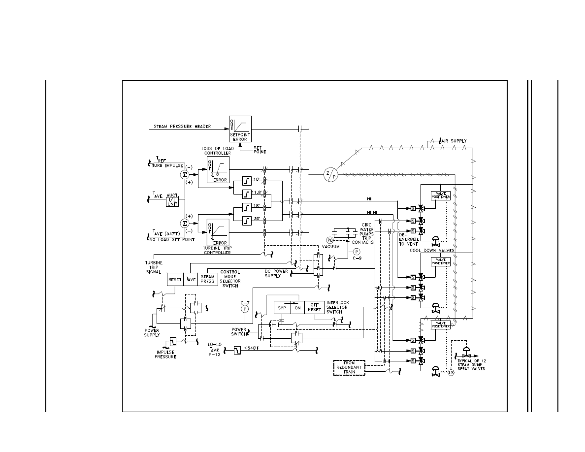
Figure 14 provides a sample illustration of how the various types of drawings can be combined.
In this example, mechanical symbols are used to represent the process system and the valves
controlled by the electrical circuit; electrical single line symbols are used to show the solenoid
relays and contacts used in the system; and electronic block symbols are used for the controllers,
summers, I/P converter, and bistables.
DOE-HDBK-1016/2-93
Electronic Diagrams and Schematics
ELECTRONIC DIAGRAMS, PRINTS, AND SCHEMATICS
Rev. 0
Page 15
PR-04
Figure 14 Example of a Combined Drawing, P&ID, Electrical Single Line, and Electronic Block Diagram
DOE-HDBK-1016/2-93
ELECTRONIC DIAGRAMS, PRINTS, AND SCHEMATICS
Electronic Diagrams and Schematics
PR-04
Page 16
Rev. 0
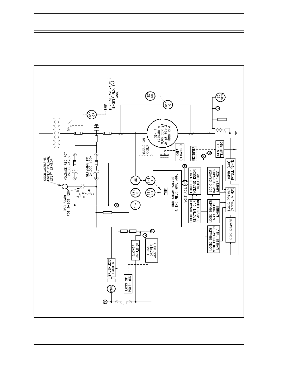
Figure 15 Example Combination Diagram of Electrical Single Line, and Block Diagram
Figure 15 illustrates the use of an electronic block diagram combined with an electrical single line
diagram. This drawing represents a portion of the generator protection circuitry of a nuclear
power generating plant.
DOE-HDBK-1016/2-93
Electronic Diagrams and Schematics
ELECTRONIC DIAGRAMS, PRINTS, AND SCHEMATICS
Rev. 0
Page 17
PR-04
Electronic Diagrams, Prints, and Schematics Summary
This chapter covered the common symbols used to represent the basic electronic
components used on electronic diagrams, prints, and schematics.
A block diagram presents the flow or functional information about a circuit, but it
is not a detailed depiction of the circuit.
An electronic schematic diagram presents the detailed information about the circuit,
each of its components, and how they are wired into the circuit.
The important information in this chapter is summarized below.

EXAMPLES
DOE-HDBK-1016/2-93
Electronic Diagrams and Schematics
This chapter provides
module.
several exercises to reinforce the material presented in this
To assist in your understanding of reading symbols and schematics, answer the following
following figures. The answers to each example are given on the page
questions concerning the
following the questions.
PR-04
Page 18
Rev. 0
Electronic Diagrams and Schematics
DOE-HDBK-1016/2-93
EXAMPLES
Rev. 0
Page 19
P R - 0 4

EXAMPLES
DOE-HDBK-1016/2-93
Electronic Diagrams and Schematics
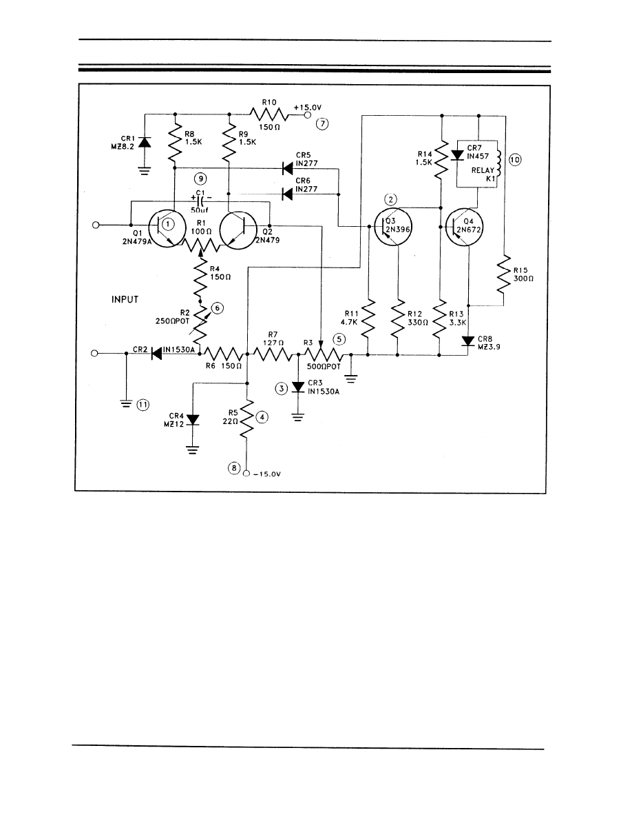
Refer to Figure 16 to answer the following:
1.
List the number which corresponds to
c .
a.
b.
d.
e.
f.
h.
g.
.
j.
i.
k.
coil or inductor
PNP transistor
diode
positive power supply
fixed resistor
capacitor
NPN transistor
variable resistor
negative power supply
circuit ground
potentiometer
the listed component.
2.
What is the value of R13? (Include units)
3.
With the input to Q1 at -15 volts, will the transistor be conducting or nonconducting?
Why?
4.
What is the value of C1? (Include units)
PR-04
Page 20
Rev. 0

Electronic Diagrams and Schematics
DOE-HDBK-1016/2-93
EXAMPLES
Answers to questions
1.
a.10 d. 7
b . 2 e . 4
c . 3 f . 9
on Figure 16
g.1
j. 11
h.6 k. 5
i . 8
2.
3.3 kilo-ohm, or 3300 ohms.
3.
Nonconducting, because the potential of the base (-15 v) is not positive relative to the
emitter (-15 v).
4.
50 microfarads or 0.000050 farads.
Rev. 0
Page 21
PR-04
EXAMPLES
DOE-HDBK-1016/2-93
Electronic Diagrams and Schematics
b.
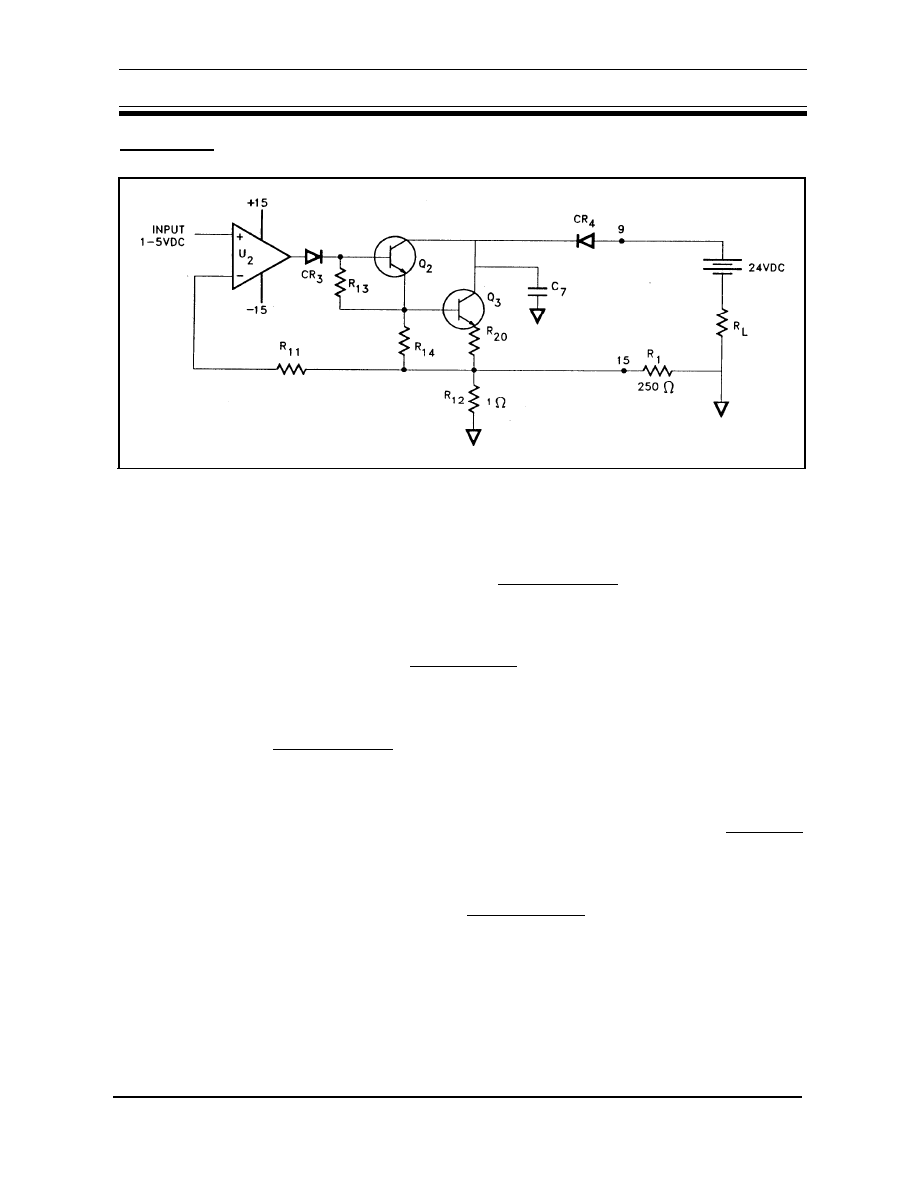
Refer to Figure 17 to answer the following:
a.
How many resistors are there in the circuit?
How many transistors are there?
, and are they PNP or NPN transistors?
c.
d.
e.
f.
What is CR
4
?
How many power supplies are there feeding the circuit and its components?
How many capacitors are in the circuit?
Q
2
will conduct when the output of U
2
is a positive or negative voltage?
PR-04
Page 22
Rev. 0

Electronic Diagram and Schematics
DOE-HDBK-1016/2-93
EXAMPLES
Answers to questions on Figure 17
a .
Seven resistors, R11, R13, R14, R20,
b.
Two, both are NPN type transistors.
c.
Diode
R12, Rl, RL
d.
Two power supplies, a 1-5 VDC to the U
2
amplifier and 24 VDC battery in the circuit.
e.
One, C
7
f.
NPN transistors conduct when their base junction is positive
The important information in this chapter is summarized below.
Exercise Summary
This chapter reviewed the material presented in this module through
practice print reading exercises.
Rev. 0
Page 23
PR-04

EXAMPLES
DOE-HDBK-1016/2-93
Electronic Diagrams and Schematics
Intentionally Left Blank
PR-04
Page 24
Rev. 0


Logic Diagrams
DOE-HDBK-1016/2-93
TABLE OF CONTENTS
TABLE OF CONTENTS
LIST OF FIGURES . . . . . . . . . . . . . . . . . . . . . . . . . . . . . . . . . . . . . . . . . . . . . . . . . . ii
LIST OF TABLES . . . . . . . . . . . . . . . . . . . . . . . . . . . . . . . . . . . . . . . . . . . . . . . . . . . iii
REFERENCES . . . . . . . . . . . . . . . . . . . . . . . . . . . . . . . . . . . . . . . . . . . . . . . . . . . .
OBJECTIVES . . . . . . . . . . . . . . . . . . . . . . . . . . . . . . . . . . . . . . . . . . . . . . . . . . . . .
ENGINEERING LOGIC DIAGRAMS . . . . . . . . . . . . . . . . . . . . . . . . . . . . . . . . . . . .
Introduction . . . . . . . . . . . . . . . . . . . . . . . . . . . . . . . . . . . . . . . . . . . . . . . . .
Symbology . . . . . . . . . . . . . . . . . . . . . . . . . . . . . . . . . . . . . . . . . . . . . . . . . .
Time Delays . . . . . . . . . . . . . . . . . . . . . . . . . . . . . . . . . . . . . . . . . . . . . . . . .
Complex Logic Devices . . . . . . . . . . . . . . . . . . . . . . . . . . . . . . . . . . . . . . . . .
Summary . . . . . . . . . . . . . . . . . . . . . . . . . . . . . . . . . . . . . . . . . . . . . . . . . . . 10
TRUTH TABLES AND EXERCISES . . . . . . . . . . . . . . . . . . . . . . . . . . . . . . . . . . . . 11
Truth Tables . . . . . . . . . . . . . . . . . . . . . . . . . . . . . . . . . . . . . . . . . . . . . . . . . 11
Reading Logic Diagrams . . . . . . . . . . . . . . . . . . . . . . . . . . . . . . . . . . . . . . . . 13
Examples . . . . . . . . . . . . . . . . . . . . . . . . . . . . . . . . . . . . . . . . . . . . . . . . . . . 13
Example 1 . . . . . . . . . . . . . . . . . . . . . . . . . . . . . . . . . . . . . . . . . . . . . . . . . . 14
Example 2 . . . . . . . . . . . . . . . . . . . . . . . . . . . . . . . . . . . . . . . . . . . . . . . . . . 16
Summary . . . . . . . . . . . . . . . . . . . . . . . . . . . . . . . . . . . . . . . . . . . . . . . . . . . 20
Rev. 0
Page i
PR-05

LIST OF FIGURES
DOE-HDBK-1016/2-93
Logic Diagrams
Figure 1 Example of a Pump Start Circuit Schematic Diagram . . . . . . . . . . . . . . . . . . . . 2
Figure 2 Example of Pump Start Circuit as a Logic Diagram . . . . . . . . . . . . . . . . . . . . . 3
Figure 3 Basic Logic Symbols . . . . . . . . . . . . . . . . . . . . . . . . . . . . . . . . . . . . . . . . . . 5
Figure 4 Conventions for Depicting Multiple Inputs . . . . . . . . . . . . . . . . . . . . . . . . . . . 5
Figure 5 COINCIDENCE Gate
. . . . . . . . . . . . . . . . . . . . . . . . . . . . . . . . . . . . . . . . . 6
Figure 6 EXCLUSIVE OR and EXCLUSIVE NOR Gates . . . . . . . . . . . . . . . . . . . . . . . 6
Figure 7 Type One Time Delay Device . . . . . . . . . . . . . . . . . . . . . . . . . . . . . . . . . . . . 7
Figure 8 Type Two Time Delay Device . . . . . . . . . . . . . . . . . . . . . . . . . . . . . . . . . . . 7
Figure 9 Type Three Time Delay Device . . . . . . . . . . . . . . . . . . . . . . . . . . . . . . . . . . . 8
Figure 10 Symbols for Complex Logic Devices . . . . . . . . . . . . . . . . . . . . . . . . . . . . . . 9
Figure 11 Truth Tables . . . . . . . . . . . . . . . . . . . . . . . . . . . . . . . . . . . . . . . . . . . . . . 12
Figure 12 Logic Gate Status Notation . . . . . . . . . . . . . . . . . . . . . . . . . . . . . . . . . . . . 13
Figure 13 Example 1 . . . . . . . . . . . . . . . . . . . . . . . . . . . . . . . . . . . . . . . . . . . . . . . . 14
Figure 14 Example 2 . . . . . . . . . . . . . . . . . . . . . . . . . . . . . . . . . . . . . . . . . . . . . . . . 16
PR-05
Page ii
Rev. 0

REFERENCES
DOE-HDBK-1016/2-93
Logic Diagrams
ANSI Y14.5M - 1982, Dimensioning and Tolerancing, American National Standards
Institute.
ANSI Y32.2 - 1975, Graphic Symbols for Electrical and Electronic Diagrams, American
National Standards Institute.
Gasperini, Richard E., Digital Troubleshooting, Movonics Company; Los Altos,
California, 1976.
Jensen - Helsel, Engineering Drawing and Design, Second Ed., McGraw-Hill Book
Company, New York, 1979.
Lenk, John D., Handbook of Logic Circuits, Reston Publishing Company, Reston,
Virginia, 1972.
Wickes, William E., Logic Design with Integrated Circuits, John Wiley & Sons, Inc,
1968.
Naval Auxiliary Machinery, United States Naval Institute, Annapolis, Maryland, 1951.
TPC Training Systems, Reading Schematics and Symbols, Technical Publishing Company,
Barrington, Illinois, 1974.
Arnell, Alvin, Standard Graphical Symbols, McGraw-Hill Book Company, 1963.
George Mashe, Systems Summary of a Westinghouse Pressurized Water Reactor,
Westinghouse Electric Corporation, 1971.
Zappe, R.W., Valve Selection Handbook, Gulf Publishing Company, Houston, Texas,
1968.
PR-05
Page iv
Rev. 0

Logic Diagrams
DOE-HDBK-1016/2-93
OBJECTIVES
1.0
Given a logic diagram, READ and INTERPRET the diagrams.
1.1
IDENTIFY the symbols used on logic diagrams to represent the following components:
a.
AND gate
h.
Adder
b.
NAND gate
i.
Time-delay
c.
COINCIDENCE gate
j.
Counter
d.
OR gate
k.
Shift register
e.
NOR gate
l.
Flip-flop
f.
EXCLUSIVE OR gate
m.
Logic memories
g.
NOT gate or inverter
1.2
EXPLAIN the operation of the three types of time delay devices.
1.3
DEVELOP the truth tables for the following logic gates:
a.
AND gate
d.
NAND gate
b.
OR gate
e.
NOR gate
c.
NOT gate
f.
EXCLUSIVE OR gate
1.4
IDENTIFY the symbols used to denote a logical 1 (or high) and a logical 0 (or low) as
used in logic diagrams.
1.5
Given a logic diagram and appropriate information, DETERMINE the output of each
component and the logic circuit.
Rev. 0
Page v
PR-05

DOE-HDBK-1016/2-93
Logic Diagrams
Intentionally Left Blank.
PR-05
Page vi
Rev. 0

Logic Diagrams
DOE-HDBK-1016/2-93
ENGINEERING LOGIC DIAGRAMS
Rev. 0
Page 1
PR-05
This chapter will review the symbols and conventions used on logic diagrams.
EO 1.1
IDENTIFY the symbols used on logic diagrams to represent
the following components:
a.
AND gate
h.
Adder
b.
NAND gate
i.
Time-delay
c.
COINCIDENCE gate
j.
Counter
d.
OR gate
k.
Shift register
e.
NOR gate
l.
Flip-flop
f.
EXCLUSIVE OR gate
m.
Logic memories
g.
NOT gate or inverter
EO 1.2
EXPLAIN the operation of the three types of time delay
devices.
Logic diagrams have many uses. In the solid state industry, they are used as the principal
diagram for the design of solid state components such as computer chips. They are used by
mathematicians to help solve logical problems (called boolean algebra). However, their principle
application at DOE facilities is their ability to present component and system operational
information. The use of logic symbology results in a diagram that allows the user to determine
the operation of a given component or system as the various input signals change.
To read and interpret logic diagrams, the reader must understand what each of the specialized
symbols represent. This chapter discusses the common symbols used on logic diagrams. When
mastered, this knowledge should enable the reader to understand most logic diagrams.
Facility operators and technical staff personnel commonly see logic symbols on equipment
diagrams. The logic symbols, called gates, depict the operation/start/stop circuits of components
and systems. The following two figures, which use a common facility start/stop pump circuit
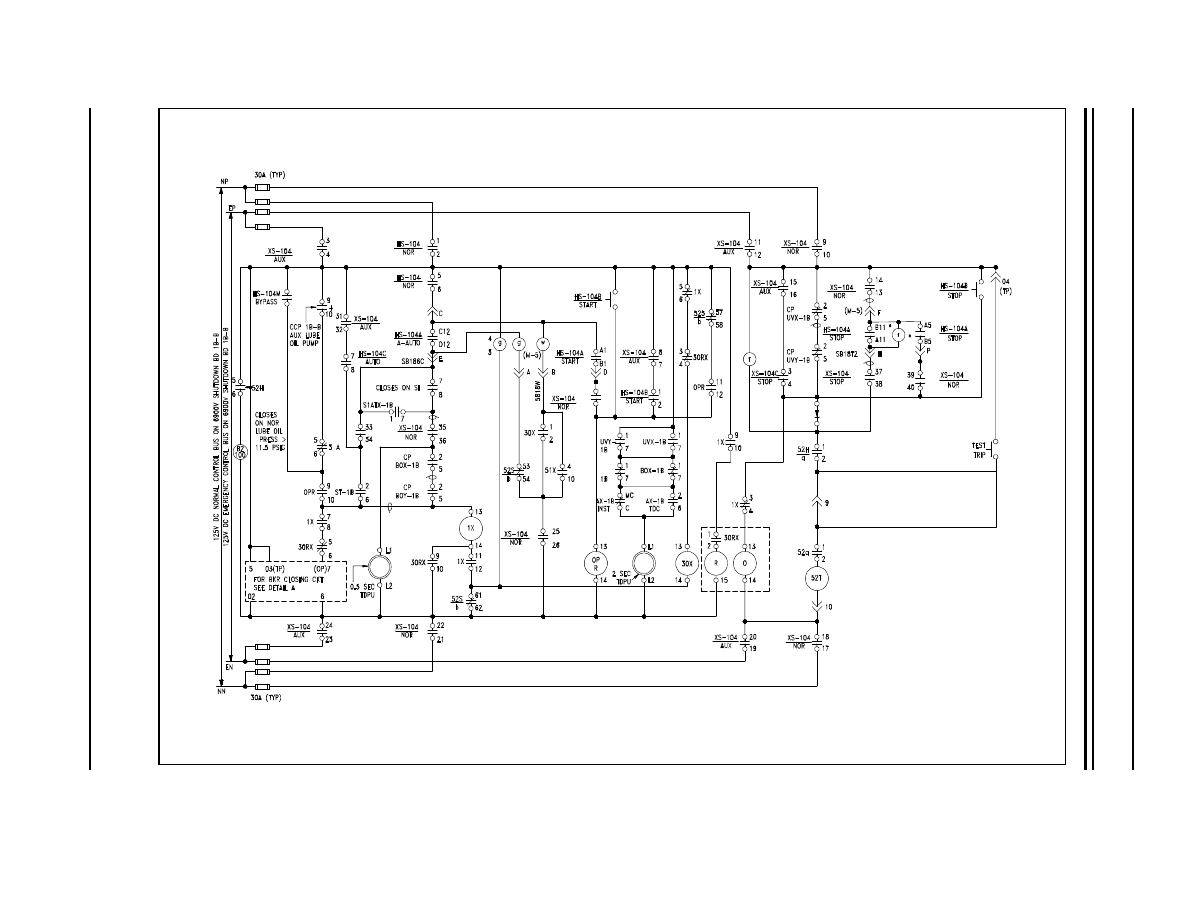
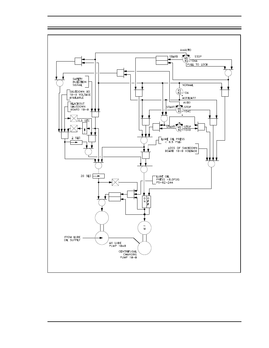
as an example, clearly demonstrate the reasons for learning to read logic diagrams. Figure 1
presents a schematic for a large pump, and Figure 2 shows the same pump circuit using only
logic gates. It is obvious that when the basic logic symbols are understood, figuring out how
the pump operates and how it will respond to various combinations of inputs using the logic
diagram is fast and easy, as compared to laboriously tracing through the relays and contacts of
the schematic diagram for the same information.
ENGINEERING LOGIC DIAGRAMS
DOE-HDBK-1016/2-93
Logic Diagrams
PR-05
Page 2
Rev. 0
Logic Diagrams
DOE-HDBK-1016/2-93
ENGINEERING LOGIC DIAGRAMS
Rev. 0
Page 3
PR-05
Figure 2 Example of Figure 1 Pump Start Circuit as a Logic Diagram

ENGINEERING LOGIC DIAGRAMS
DOE-HDBK-1016/2-93
Logic Diagrams
PR-05
Page 4
Rev. 0
There are three basic types of logic gates. They are AND, OR, and NOT gates. Each gate
is a very simple device that only has two states, on and off. The states of a gate are also
commonly referred to as high or low, 1 or 0, or True or False, where on = high = 1 = True,
and off = low = 0 = False. The state of the gate, also referred to as its output, is determined
by the status of the inputs to the gate, with each type of gate responding differently to the
various possible combinations of inputs. Specifically, these combinations are as follows.
AND gate - provides an output (on) when all its inputs are on. When any one of the
inputs is off, the gate's output is off.
OR gate - provides an output (on) when any one or more of its inputs is on. The gate
is off only when all of its inputs are off.
NOT gate - provides a reversal of the input. If the input is on, the output will be off.
If the input is off, the output will be on.
Because the NOT gate is frequently used in conjunction with AND and OR gates, special
symbols have been developed to represent these combinations. The combination of an AND
gate and a NOT gate is called a NAND gate. The combination of an OR gate with a NOT
gate is called a NOR gate.
NAND gate - is the opposite (NOT) of an AND gate's output. It provides an output
(on) except when all the inputs are on.
NOR gate - is the opposite (NOT) of an OR gate's output. It provides an output only
when all inputs are off.
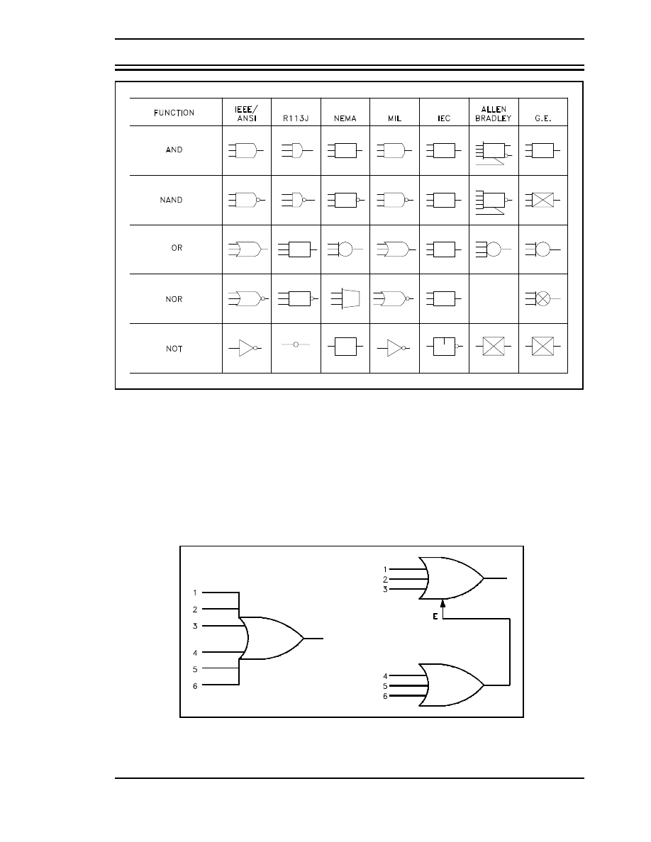
Figure 3 illustrates the symbols covering the three basic logic gates plus NAND and NOR
gates. The IEEE/ANSI symbols are used most often; however, other symbol conventions are
provided on Figure 3 for information.
Logic Diagrams
DOE-HDBK-1016/2-93
ENGINEERING LOGIC DIAGRAMS
Rev. 0
Page 5
PR-05
Figure 4 Conventions for Depicting Multiple Inputs
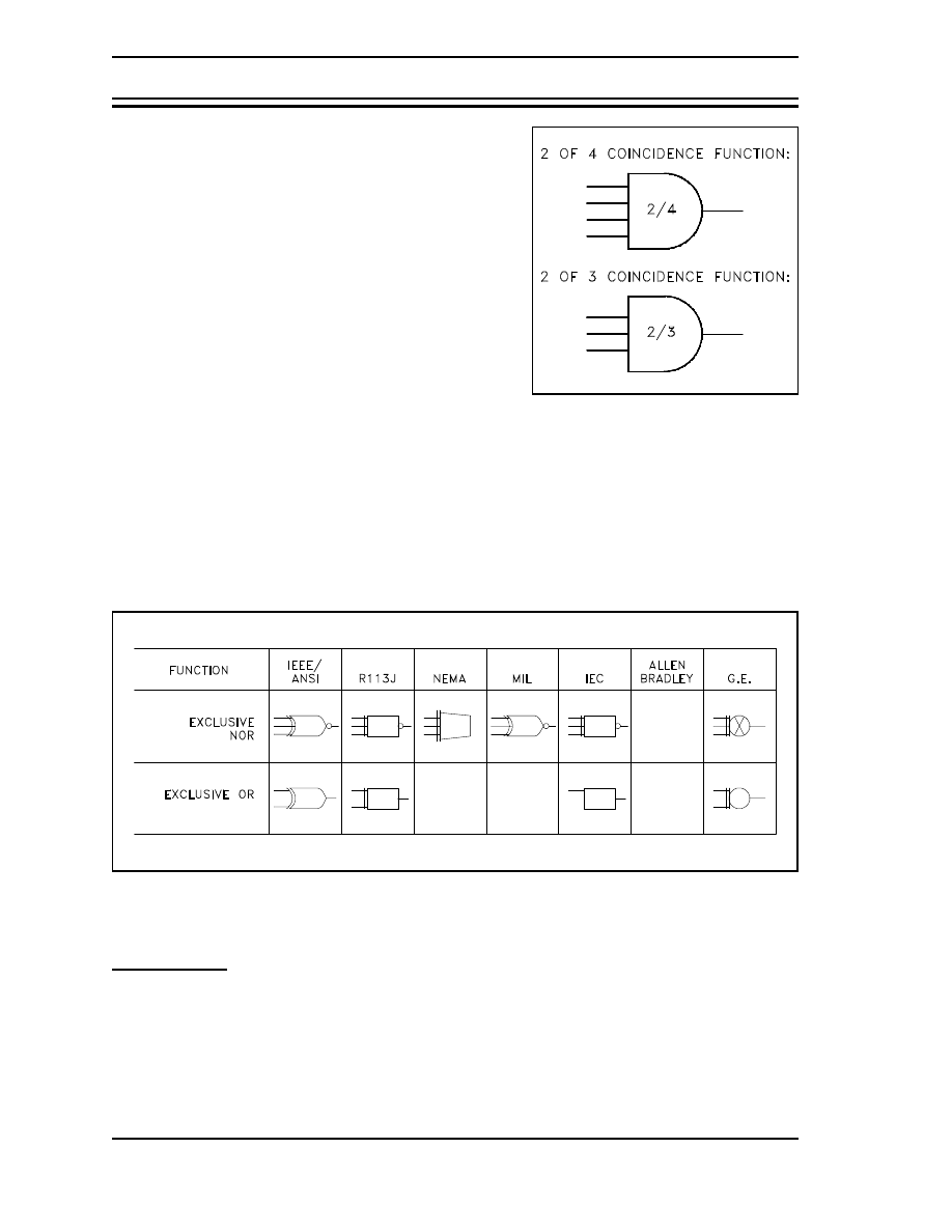
The AND gate has a common variation called a COINCIDENCE gate. Logic gates are not
limited to two inputs. Theoretically, there is no limit to the number of inputs a gate can have.
But, as the number of inputs increases, the symbol must be altered to accommodate the
increased inputs. There are two basic ways to show multiple inputs. Figure 4 demonstrates
both methods, using an OR gate as an example. The symbols used in Figure 4 are used
extensively in computer logic diagrams. Process control logic diagrams usually use the
symbology shown in Figure 2.
ENGINEERING LOGIC DIAGRAMS
DOE-HDBK-1016/2-93
Logic Diagrams
PR-05
Page 6
Rev. 0
Figure 6 EXCLUSIVE OR and EXCLUSIVE NOR Gates
The COINCIDENCE gate behaves like an AND gate
except that only a specific number of the total number
of inputs needs to be on for the gate's output to be on.
The symbol for a COINCIDENCE gate is shown in
Figure 5. The fraction in the logic symbol indicates that
the AND gate is a COINCIDENCE gate. The
numerator of the fraction indicates the number of inputs
that must be on for the gate to be on. The denominator
states the total number of inputs to the gate.
Two variations of the OR gate are the EXCLUSIVE
OR and its opposite, the EXCLUSIVE NOR. The
EXCLUSIVE OR and the EXCLUSIVE NOR are
symbolized by adding a line on the back of the standard
OR or NOR gate's symbol, as illustrated in Figure 6.
EXCLUSIVE OR - provides an output (on) when only one of the inputs is on. Any
other combination results in no output (off).
EXCLUSIVE NOR - is the opposite (NOT) of an EXCLUSIVE OR gate's output. It
provides an output only when all inputs are on or when all inputs are off.
When logic diagrams are used to represent start/stop/operate circuits, the diagrams must also
be able to symbolize the various timing devices found in the actual circuits. There are three
major types of timers. They are 1) the Type-One Time Delay Device, 2) the Type-Two Time
Delay Device, and 3) The Type-Three Time Delay Device.
Logic Diagrams
DOE-HDBK-1016/2-93
ENGINEERING LOGIC DIAGRAMS
Rev. 0
Page 7
PR-05
Figure 7 Type One Time Delay Device
Figure 8 Type Two Time Delay Device
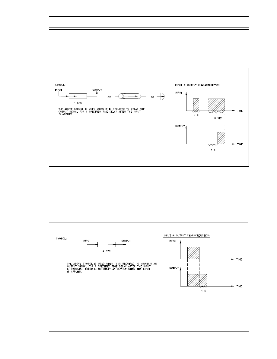
Upon receipt of the input signal, the Type-One Time Delay Device delays the output
(on) for the specified period of time, but the output will stop (off) as soon as the input
signal is removed, as illustrated by Figure 7. The symbol for this type of timer is
illustrated in Figure 7.
The Type-Two Time Delay Device provides an output signal (on) immediately upon
reciept of the input signal, but the output is maintained only for a specified period of
time once the input signal (off) has been removed. Figure 8 demonstrates the signal
response, and Figure 8 illustrates the symbol used to denote this type of timer.
ENGINEERING LOGIC DIAGRAMS
DOE-HDBK-1016/2-93
Logic Diagrams
PR-05
Page 8
Rev. 0
Figure 9 Type-Three Time Delay Device
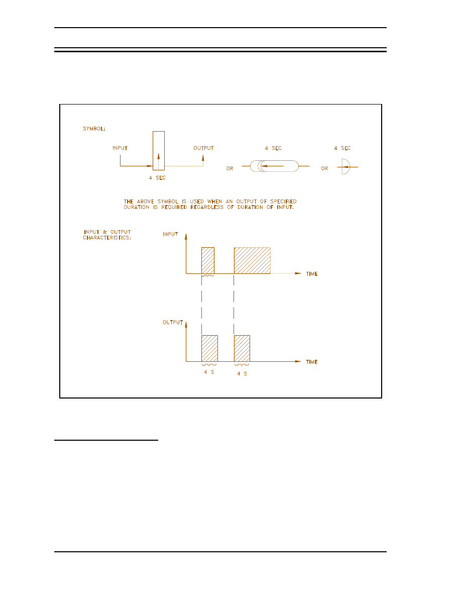
Upon reciept of an input signal, Type-Three Time Delay Devices provide an output
signal for a specified period of time, regardless of the duration of the input. Figure 9
demonstrates the signal response and illustrates the symbol used to denote the timer.
In addition to the seven basic logic gates, there are several complex logic devices that may be
encountered in the use of logic prints.
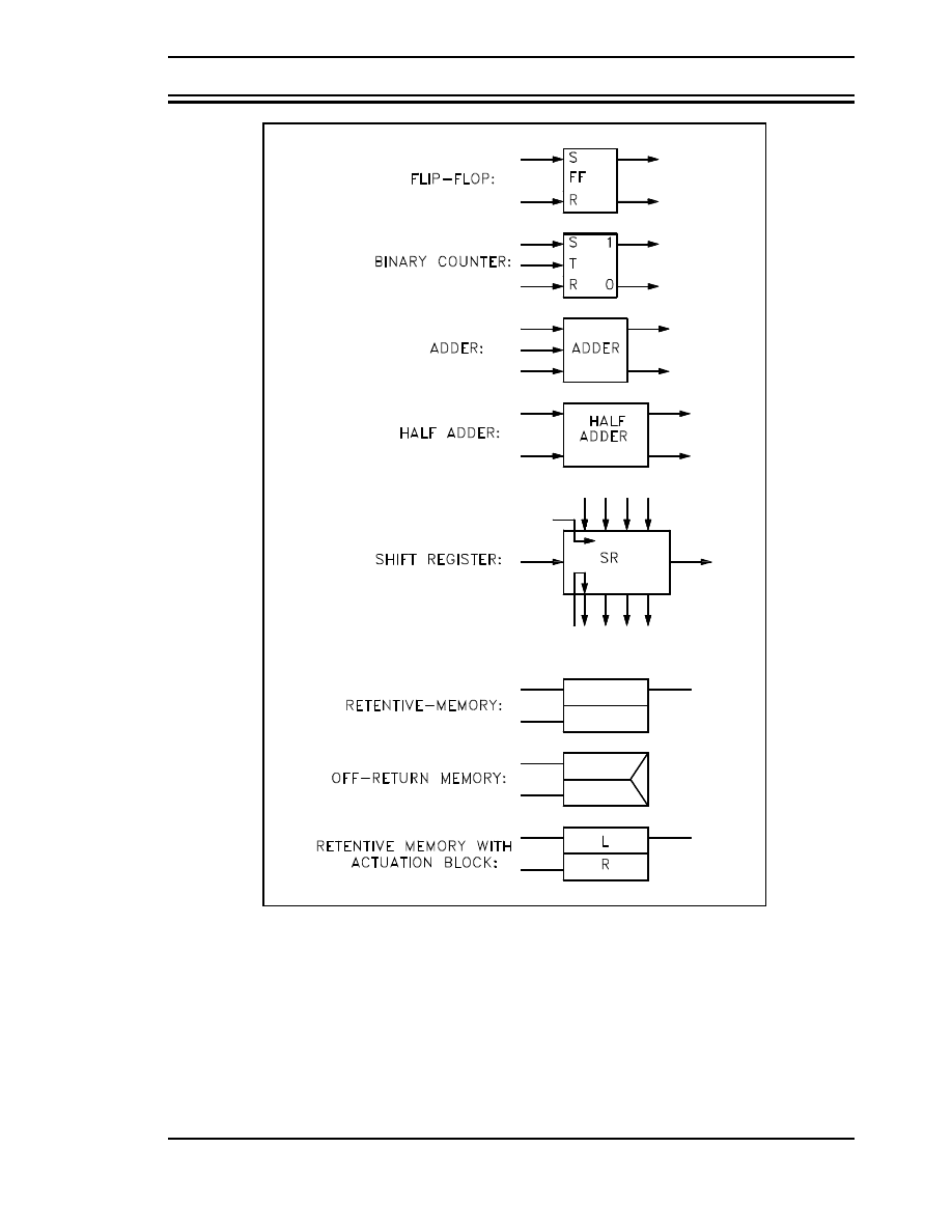
Memory devices - In many circuits, a device that can "remember" the last command or
the last position is required for a circuit to function. Like the AND and OR gates,
memory devices have been designed to work with on/off signals. The two input signals
to a memory device are called set and reset. Figure 10 shows the common symbols
used for memory devices.
Logic Diagrams
DOE-HDBK-1016/2-93
ENGINEERING LOGIC DIAGRAMS
Rev. 0
Page 9
PR-05
Figure 10 Symbols for Complex Logic Devices
Flop-flop - As the name implies, a flip-flop is a device in which as one or more of its
inputs changes, the output changes. A flip-flop is a complex circuit constructed from
OR and NOT gates, but is used so frequently in complex circuits that it has its own
symbol. Figure 10 shows the common symbol used for a flip-flop.
ENGINEERING LOGIC DIAGRAMS
DOE-HDBK-1016/2-93
Logic Diagrams
PR-05
Page 10
Rev. 0
Engineering Logic Diagrams Summary
This chapter reviewed the seven basic symbols used on logic diagrams and the
symbols used for six of the more complex logic devices.
There are three types of time delay devices:
Type One - delays the output signal for a specified period of time
Type Two - only generates an output for the specified period of time
Type Three - receipt of an input signal triggers the device to output a
signal for the specified time, regardless of the duration of the input
This device, although occasionally used on component and system type logic diagrams,
is principally used in solid state logic diagrams (computers).
Binary counter - Several types of binary counters exist, all of which are constructed of
flip-flops. The purpose of a counter is to allow a computer to count higher than 1,
which is the highest number a single flip-flop can represent. By ganging flip-flops,
higher binary numbers can be constructed. Figure 10 illustrates a common symbol used
for a binary counter.
Shift register - Is a storage device constructed of flip-flops that is used in computers to
provide temporary storage of a binary word. Figure 10 shows the common symbol used
for a shift register.
Half adder - Is a logic circuit that is used in computer circuits to allow the computer to
"carry" numbers when it is performing mathematical operations (for example to perform
the addition of 9 + 2, a single 10s unit must be "carried" from the ones column to the
tens column). Figure 10 illustrates the symbol used for a half adder.
The important information in this chapter is summarized below.

Logic Diagrams
DOE-HDBK-1016/2-93
TRUTH TABLES AND EXERCISES
Rev. 0
Page 11
PR-05
Truth tables offer a simple and easy to understand tool that can be used to
determine the output of any logic gate or circuit for all input combinations.
EO 1.3
DEVELOP the truth tables for the following logic gates:
a.
AND gate
d.
NAND gate
b.
OR gate
e.
NOR gate
c.
NOT gate
f.
EXCLUSIVE OR gate
EO 1.4
IDENTIFY the symbols used to denote a logical 1 (or high)
and a logical 0 (or low) as used in logic diagrams.
EO 1.5
Given a logic diagram and appropriate information,
DETERMINE the output of each component and the logic
circuit.
When a logic gate has only two inputs, or the logic circuit to be analyzed has only one or two
gates, it is fairly easy to remember how a specific gate responds and determine the output of
the gate or circuit. But as the number of inputs and/or the complexity of the circuit grows, it
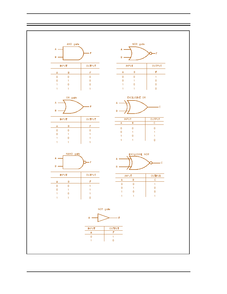
becomes more difficult to determine the output of the gate or circuit. Truth tables, as illustrated
in Figure 11, are tools designed to help solve this problem. A truth table has a column for the
input of each gate and column for the output of each gate. The number of rows needed is based
on the number of inputs, so that every combination of input signal is listed (mathematically the
number of rows is 2 , where n = number of inputs). In truth tables, the on and off status of the
n
inputs and outputs is represented using 0s and 1s. As previously stated 0 = off and 1 = on.
Figure 11 lists truth tables for the seven basic logic gates. Compare each gate's truth table with
its definition given earlier in this module, and verify for yourself that they are stating the same
thing.
TRUTH TABLES AND EXERCISES
DOE-HDBK-1016/2-93
Logic Diagrams
PR-05
Page 12
Rev. 0
Logic Diagrams
DOE-HDBK-1016/2-93
TRUTH TABLES AND EXERCISES
Rev. 0
Page 13
PR-05
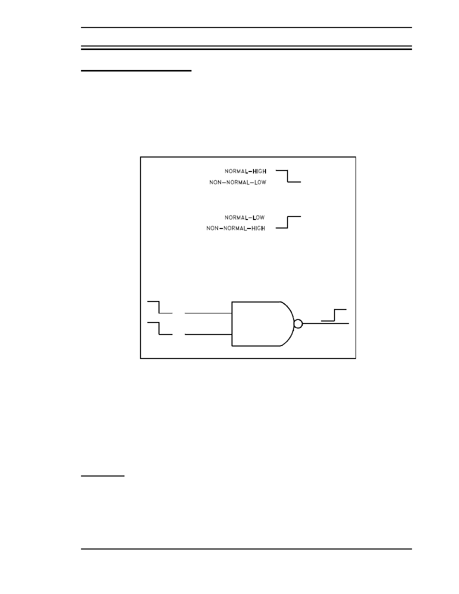
Figure 12 Logic Gate Status Notation
When reading logic prints the reader usually must decide the input values to each gate. But
occasionally the print will provide information as to the normal state of each logic gate. This
is denoted by a symbol similar to the bistable symbol, as shown in Figure 12. The symbol is
drawn so that the first part of the square wave indicates the normal state of the gate. The
second part of the square wave indicates the off-normal state of the gate. Figure 12 also
illustrates how this notation is applied.
Reading a logic diagram that does not provide information on the status of the gates is not any
more difficult. It simply requires the reader to choose the initial conditions, determine the
response of the circuits, and modify the inputs as needed. The following exercises will illustrate
how to read some simple logic diagrams.
To aid in understanding the material presented in this module, practice reading the following
logic diagrams by answering the questions. The answers are on page 18.
TRUTH TABLES AND EXERCISES
DOE-HDBK-1016/2-93
Logic Diagrams
PR-05
Page 14
Rev. 0
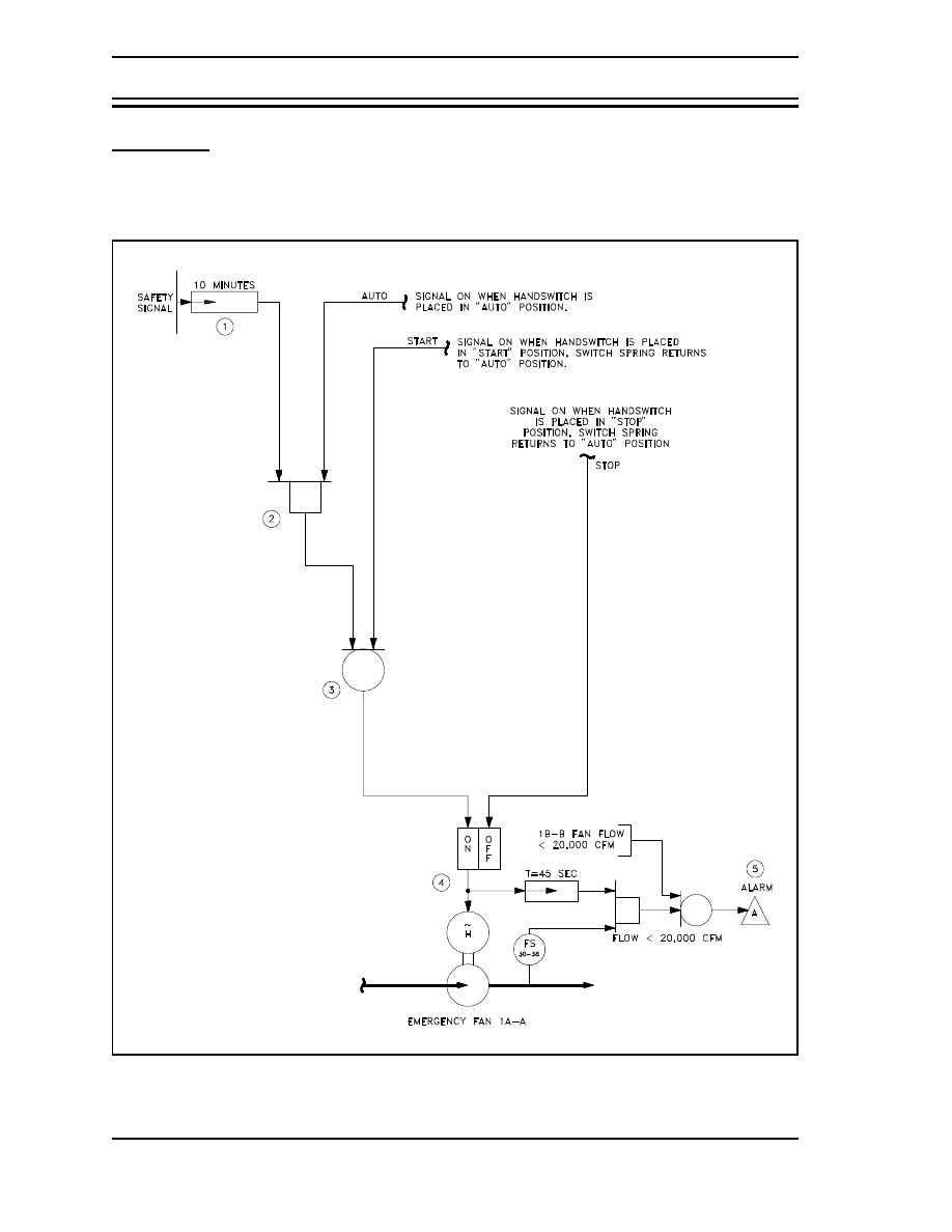
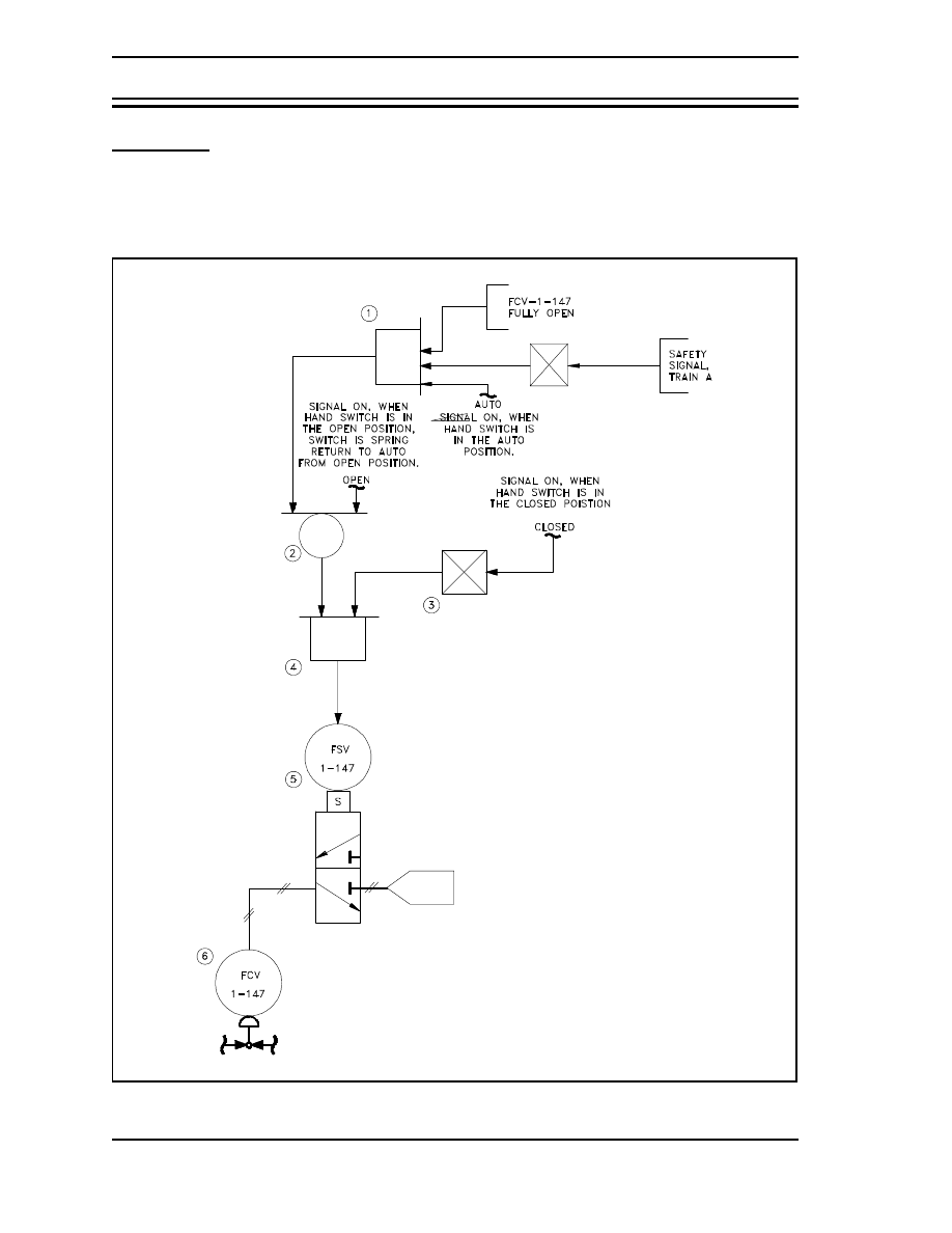
Refer to Figure 13 to answer the following questions. Figure 13 illustrates a logic diagram of
a simple fan start circuit.

Logic Diagrams
DOE-HDBK-1016/2-93
TRUTH TABLES AND EXERCISES
Rev. 0
Page 15
PR-05
1.
Identify by number the following logic symbols:
a.
AND
b.
OR
c.
Time delay
d.
Retentive-Memory
2.
How long must the safety signal be present before the time delay (1) will pass an output
(on) signal to Gate 2?
3.
Under what conditions will Gate 2 turn on?
4.
Under what conditions will the low flow alarm (5) sound?
5.
Since the control switch is always in the AUTO position (due to the spring return
feature), what logic gate keeps the continuous on signal that is generated by the control
switch being in the AUTO position from starting the fan? What signal must also be
present to allow the AUTO signal to start the fan?
6.
If 12 minutes after first receiving a safety signal, with the fan control switch in the
AUTO position, the safety signal is removed (off), what will happen to the fan? Why?
7.
How many ways can the fan be started? How many ways can the fan be stopped?
TRUTH TABLES AND EXERCISES
DOE-HDBK-1016/2-93
Logic Diagrams
PR-05
Page 16
Rev. 0
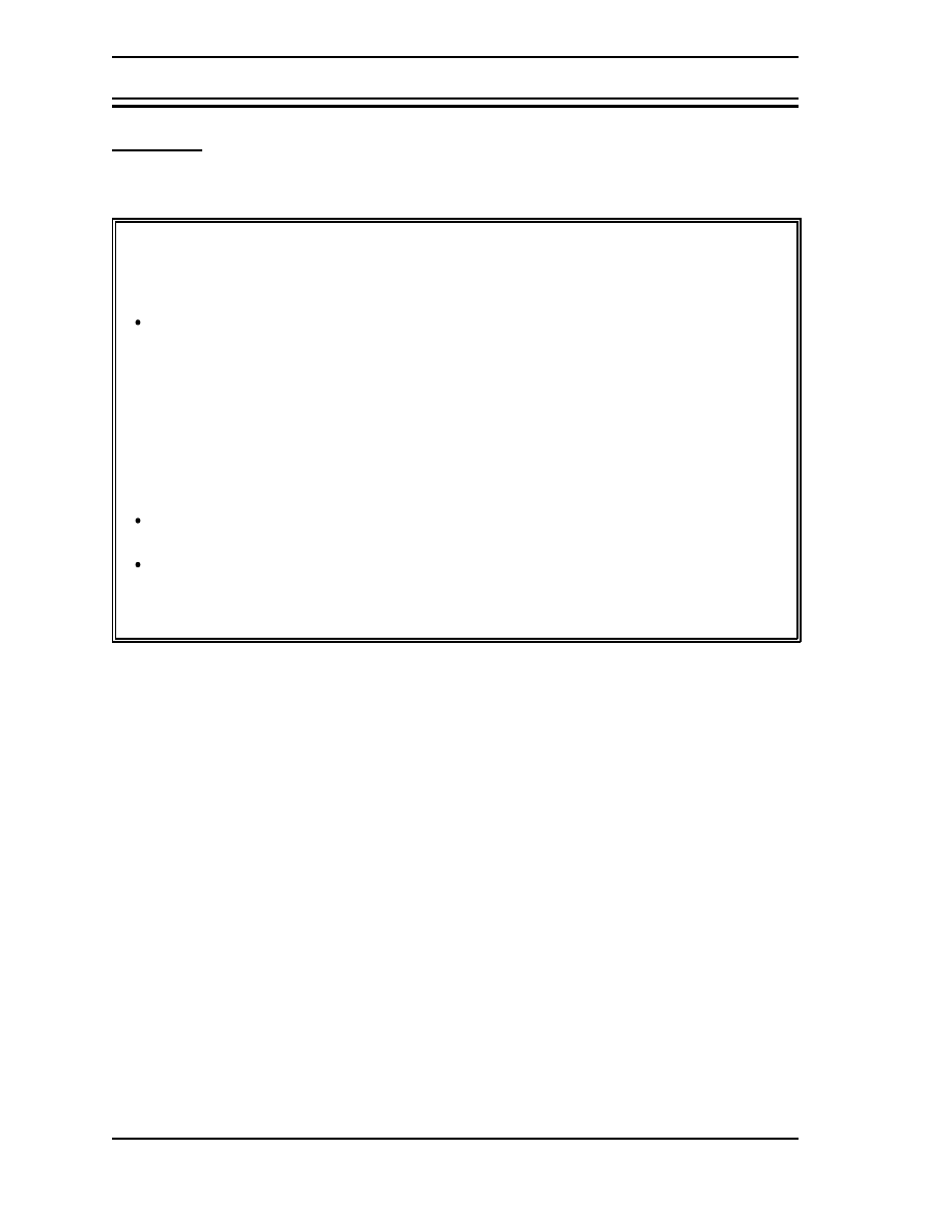
Refer to Figure 14 to answer the following questions. Figure 14 illustrates a simple valve
control circuit. Flow control valve (FCV) 1-147 is an air-operated valve, with its air controlled
by flow solenoid valve (FSV) 1-147, which is shown in its de-energized position.

Logic Diagrams
DOE-HDBK-1016/2-93
TRUTH TABLES AND EXERCISES
Rev. 0
Page 17
PR-05
1.
Identify by number the following logic symbols.
a.
AND
b.
OR
c.
NOT
2.
As drawn, with the hand switch in the AUTO position and no safety signal present,
what is the status of the two inputs to Gate 4, on or off?
3.
Since electrical components are drawn in their de-energized state, and using the answer
from Question 2, is the flow solenoid valve (FSV-1-147) in its correct position? Why?
4.
How many ways can FSV-1-147 be energized? De-energized?
5.
If a safety signal is present, can FCV-1-147 (valve FSV-1-147 energized) be opened?
Why?

TRUTH TABLES AND EXERCISES
DOE-HDBK-1016/2-93
Logic Diagrams
PR-05
Page 18
Rev. 0
Answers to example 1.
1.
a. 2
b. 3
c. 1
d. 4
2.
The safety signal must be received for greater than 10 minutes before it will pass
through the time delay. If the safety signal is removed before 10 minutes has elapsed
no signal will be passed to Gate 2.
3.
Gate 2 will turn on when the hand-switch is in the AUTO position and a safety signal
has been received for greater than 10 minutes.
4.
If flow switch (FS) 30-38 senses less than 20,000 cfm, 45 seconds after the fan has
started, or the same condition exists on the 1B-B fan, the alarm will sound.
5.
AND Gate 2 prevents the on signal from passing until a safety signal is also received
(>10 minutes).
6.
Ten minutes after receiving the safety signal, the fan started. At 12 minutes, removing
the safety signal only removes the continuous start signal to the fan. The fan will
continue to run until the hand switch is placed in the stop position. Further, with the
removal of the safety signal, the fan will remain stopped when the hand switch spring
returns to the AUTO position. Note that if the hand switch is placed in the stop
position while the safety signal is present, the fan will stop, but will restart as soon as
the switch spring returns to the AUTO position.
7.
It can be started by two signals - START and AUTO plus a safety signal.
It can be stopped by one signal - STOP (but will only remain stopped if no safety signal
is present or the switch is held in the stopped position).
Answers to example number 2.
1.
a. 1 & 4
b. 2
c. 3
2.
Right input is - on - this is because the hand control switch is in the AUTO position, and
the AUTO switch contacts are made up, resulting in an on signal. Therefore the hand-
switch CLOSE position contacts are open, resulting in an off signal. The off signal is
reversed in the NOT gate and becomes an on signal.

Logic Diagrams
DOE-HDBK-1016/2-93
TRUTH TABLES AND EXERCISES
Rev. 0
Page 19
PR-05
Left input is - off -. To determine this, the status of the gates feeding the left input must
be determined.
Looking at the OR gate (2) above it
The right input to the OR gate is - off - because the hand control switch
is in the AUTO position. The OPEN position contacts are not made up,
resulting in an off signal.
The left input to the OR gate comes from the AND gate (1) above it.
Looking at the three inputs to the AND gate. The bottom input
is - on - because the hand control switch is in the AUTO position
and the AUTO contacts are made up, resulting in an on signal.
The middle input to the AND gate is - on - because the NOT gate
reverses the off safety signal.
The top input is - off - because the valve is not fully open,
resulting in the generation of an off signal. Note this is the signal
that, once the valve has traveled to the fully open position, allows
the valve to remain open after the hand switch is allowed to
spring return to the AUTO position.
Now that all the inputs are known, we can work back through the circuit to determine
the status of the left input to the AND gate (4).
Because the one input, the top, to the AND gate (1) is off, the output of
the AND gate is off. Therefore, the left input into the OR gate (2) is off.
Therefore, because both the left and right inputs to the OR gate (2) are
off the output of the OR gate (1) is off.
3.
Yes, de-energized is correct because the left input of the AND gate (4) is off and its right
input is on. But because it is an AND gate and both its inputs are not on, it will not pass
an on signal to the solenoid to energize it.
4.
It can be energized one way - the hand switch can be momentarily placed in the OPEN
position.
It can be de-energized two ways - the hand switch can be placed in the CLOSE position,
or, if the valve is open and a safety signal is received, the valve will automatically close.
5.
Yes, the valve can be opened, but it will not remain open when the hand switch is
allowed to spring return to the AUTO position. This is because the safety signal's NOT
gate removes the on signal that allows the AND gate (1) to output an on signal and
energize the solenoid.
TRUTH TABLES AND EXERCISES
DOE-HDBK-1016/2-93
Logic Diagrams
PR-05
Page 20
Rev. 0
Truth Tables and Exercises Summary
The normal and off-normal status of each logic gate can be symbolized by the use
of a symbol similar to the bistable.
The first part of the square wave indicates the normal state of
the gate.
The second part of the square wave indicates the off-normal state
of the gate.
This chapter presented the truth tables for each of the seven basic logic gates.
This chapter reviewed several examples of how to read logic diagrams of simple
pump and valve circuits.
The important information in this chapter is summarized below.

Department of Energy
Fundamentals Handbook
ENGINEERING SYMBOLOGY, PRINTS,


DOE-HDBK-1016/2-93
Engineering Fabrication, Construction, and Architectural Drawings
TABLE OF CONTENTS
TABLE OF CONTENTS
LIST OF FIGURES . . . . . . . . . . . . . . . . . . . . . . . . . . . . . . . . . . . . . . . . . . . . . . . . . . ii
LIST OF TABLES . . . . . . . . . . . . . . . . . . . . . . . . . . . . . . . . . . . . . . . . . . . . . . . . . . . iii
REFERENCES . . . . . . . . . . . . . . . . . . . . . . . . . . . . . . . . . . . . . . . . . . . . . . . . . . . .
OBJECTIVES . . . . . . . . . . . . . . . . . . . . . . . . . . . . . . . . . . . . . . . . . . . . . . . . . . . . .
ENGINEERING FABRICATION, CONSTRUCTION,
AND ARCHITECTURAL DRAWINGS . . . . . . . . . . . . . . . . . . . . . . . . . . . . . . . . . . .
Introduction . . . . . . . . . . . . . . . . . . . . . . . . . . . . . . . . . . . . . . . . . . . . . . . . .
Dimensioning Drawings . . . . . . . . . . . . . . . . . . . . . . . . . . . . . . . . . . . . . . . . .
Dimensioning and Tolerance Symbology, Rules, and Conventions
. . . . . . . . . . .
Summary . . . . . . . . . . . . . . . . . . . . . . . . . . . . . . . . . . . . . . . . . . . . . . . . . . . 12
ENGINEERING FABRICATION, CONSTRUCTION,
AND ARCHITECTURAL DRAWING, EXAMPLES . . . . . . . . . . . . . . . . . . . . . . . . . . 13
Examples . . . . . . . . . . . . . . . . . . . . . . . . . . . . . . . . . . . . . . . . . . . . . . . . . . . 13
Example 1 . . . . . . . . . . . . . . . . . . . . . . . . . . . . . . . . . . . . . . . . . . . . . . . . . . 13
Example 2 . . . . . . . . . . . . . . . . . . . . . . . . . . . . . . . . . . . . . . . . . . . . . . . . . . 14
Example 3 . . . . . . . . . . . . . . . . . . . . . . . . . . . . . . . . . . . . . . . . . . . . . . . . . . 15
Summary . . . . . . . . . . . . . . . . . . . . . . . . . . . . . . . . . . . . . . . . . . . . . . . . . . . 17
Rev. 0
Page i
PR-06

DOE-HDBK-1016/2-93
LIST OF FIGURES
Engineering Fabrication, Construction, and Architectural Drawings
Figure 1 Example of a Fabrication Drawing . . . . . . . . . . . . . . . . . . . . . . . . . . . . . . . . . 2
Figure 2 Example of a Construction Drawing . . . . . . . . . . . . . . . . . . . . . . . . . . . . . . . . 3
Figure 3 Example of an Architectural Drawing
. . . . . . . . . . . . . . . . . . . . . . . . . . . . . . 4
Figure 4 Types of Dimensioning Lines . . . . . . . . . . . . . . . . . . . . . . . . . . . . . . . . . . . . 6
Figure 5 Example of Dimensioning Notation . . . . . . . . . . . . . . . . . . . . . . . . . . . . . . . . 7
Figure 6 Symbology Used in Tolerancing Drawings . . . . . . . . . . . . . . . . . . . . . . . . . . . 9
Figure 7 Examples of Tolerance Symbology . . . . . . . . . . . . . . . . . . . . . . . . . . . . . . . 10
Figure 8 Example of Tolerancing . . . . . . . . . . . . . . . . . . . . . . . . . . . . . . . . . . . . . . . 11
Figure 9 Example 1 . . . . . . . . . . . . . . . . . . . . . . . . . . . . . . . . . . . . . . . . . . . . . . . . 13
Figure 10 Example 2 . . . . . . . . . . . . . . . . . . . . . . . . . . . . . . . . . . . . . . . . . . . . . . . . 14
Figure 11 Example 3 . . . . . . . . . . . . . . . . . . . . . . . . . . . . . . . . . . . . . . . . . . . . . . . . 15
PR-06
Page ii
Rev. 0

DOE-HDBK-1016/2-93
Engineering Fabrication, Construction, and Architectural Drawings
LIST OF TABLES
NONE
Rev. 0
Page iii
PR-06

DOE-HDBK-1016/2-93
REFERENCES
Engineering Fabrication, Construction, and Architectural Drawings
ANSI Y14.5M - 1982, Dimensioning and Tolerancing, American National Standards
Institute.
ANSI Y32.2 - 1975, Graphic Symbols for Electrical and Electronic Diagrams, American
National Standards Institute.
Gasperini, Richard E., Digital Troubleshooting, Movonics Company; Los Altos,
California, 1976.
Jensen - Helsel, Engineering Drawing and Design, Second Ed., McGraw-Hill Book
Company, New York, 1979.
Lenk, John D., Handbook of Logic Circuits, Reston Publishing Company, Reston,
Virginia, 1972.
Wickes, William E., Logic Design with Integrated Circuits, John Wiley & Sons, Inc,
1968.
Naval Auxiliary Machinery, United States Naval Institute, Annapolis, Maryland, 1951.
TPC Training Systems, Reading Schematics and Symbols, Technical Publishing Company,
Barrington, Illinois, 1974.
Arnell, Alvin, Standard Graphical Symbols, McGraw-Hill Book Company, 1963.
George Mashe, Systems Summary of a Westinghouse Pressurized Water Reactor,
Westinghouse Electric Corporation, 1971.
Zappe, R.W., Valve Selection Handbook, Gulf Publishing Company, Houston, Texas,
1968.
PR-06
Page iv
Rev. 0

DOE-HDBK-1016/2-93
Engineering Fabrication, Construction, and Architectural Drawings
OBJECTIVES
1.0
Given an engineering fabrication, construction, or architectural drawing, READ and
INTERPRET basic dimensional and tolerance symbology, and basic fabrication,
construction, or architectural symbology.
1.1
STATE the purpose of engineering fabrication, construction, and architectural drawings.
1.2
Given an engineering fabrication, construction, or architectural drawing, DETERMINE
the specified dimensions of an object.
1.3
Given an engineering fabrication, construction, or architectural drawing, DETERMINE
the maximum and minimum dimensions or location of an object or feature from the stated
drawing tolerance.
Rev. 0
Page v
PR-06

DOE-HDBK-1016/2-93
Engineering Fabrication, Construction, and Architectural Drawings
Intentionally Left Blank.
PR-06
Page vi
Rev. 0

DOE-HDBK-1016/2-93
Engineering Fabrication,
ENGINEERING FABRICATION, CONSTRUCTION,
Construction, and Architectural Drawings
AND ARCHITECTURAL DRAWINGS
Rev. 0
Page 1
PR-06
ENGINEERING FABRICATION, CONSTRUCTION,
This chapter describes the basic symbology used in the dimensions and tolerances
of engineering fabrication, construction, and architectural drawings. Knowledge
of this information will make these types of prints easier to read and understand.
EO 1.1
STATE the purpose of engineering fabrication, construction,
and architectural drawings.
EO 1.2
Given an engineering fabrication, construction, or architectural
drawing, DETERMINE the specified dimensions of an object.
EO 1.3
Given an engineering fabrication, construction, or architectural
drawing, DETERMINE the maximum and minimum
dimensions or location of an object or feature from the stated
drawing tolerance.
This chapter will describe engineering fabrication, construction, and architectural drawings.
These three types of drawings represent the category of drawings commonly referred to as
blueprints. Fabrication, construction, and architectural drawings differ from P&IDs, electrical
prints, and logic diagrams in that they are drawn to scale and provide the component's physical
dimensions so that the part, component, or structure can be manufactured or assembled.
Although fabrication and construction drawings are presented as separate categories, both supply
information about the manufacture or assembly of a component or structure. The only real
difference between the two is the subject matter. A fabrication drawing provides information
on how a single part is machined or fabricated in a machine shop, whereas a construction
drawing provides the construction or assembly of large multi-component structures or systems.
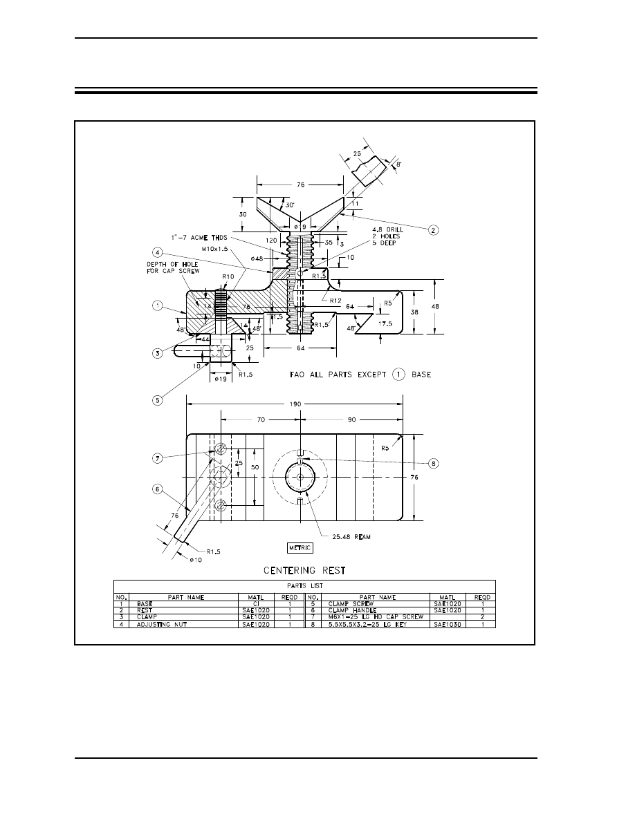
Fabrication drawings, also called machine drawings, are principally found in and around
machine and fabrication shops where the actual machine work is performed. The drawing
usually depicts the part or component as an orthographic projection (see module 1 for
definition) with each view containing the necessary dimensions. Figure 1 is an example of a
fabrication drawing. In this case, the drawing is a centering rest that is used to support material
as it is being machined.
DOE-HDBK-1016/2-93
ENGINEERING FABRICATION, CONSTRUCTION,
Engineering Fabrication,
AND ARCHITECTURAL DRAWINGS
Construction, and Architectural Drawings
PR-06
Page 2
Rev. 0
DOE-HDBK-1016/2-93
Engineering Fabrication,
ENGINEERING FABRICATION, CONSTRUCTION,
Construction, and Architectural Drawings
AND ARCHITECTURAL DRAWINGS
Rev. 0
Page 3
PR-06
Figure 2 Example of a Construction Drawing
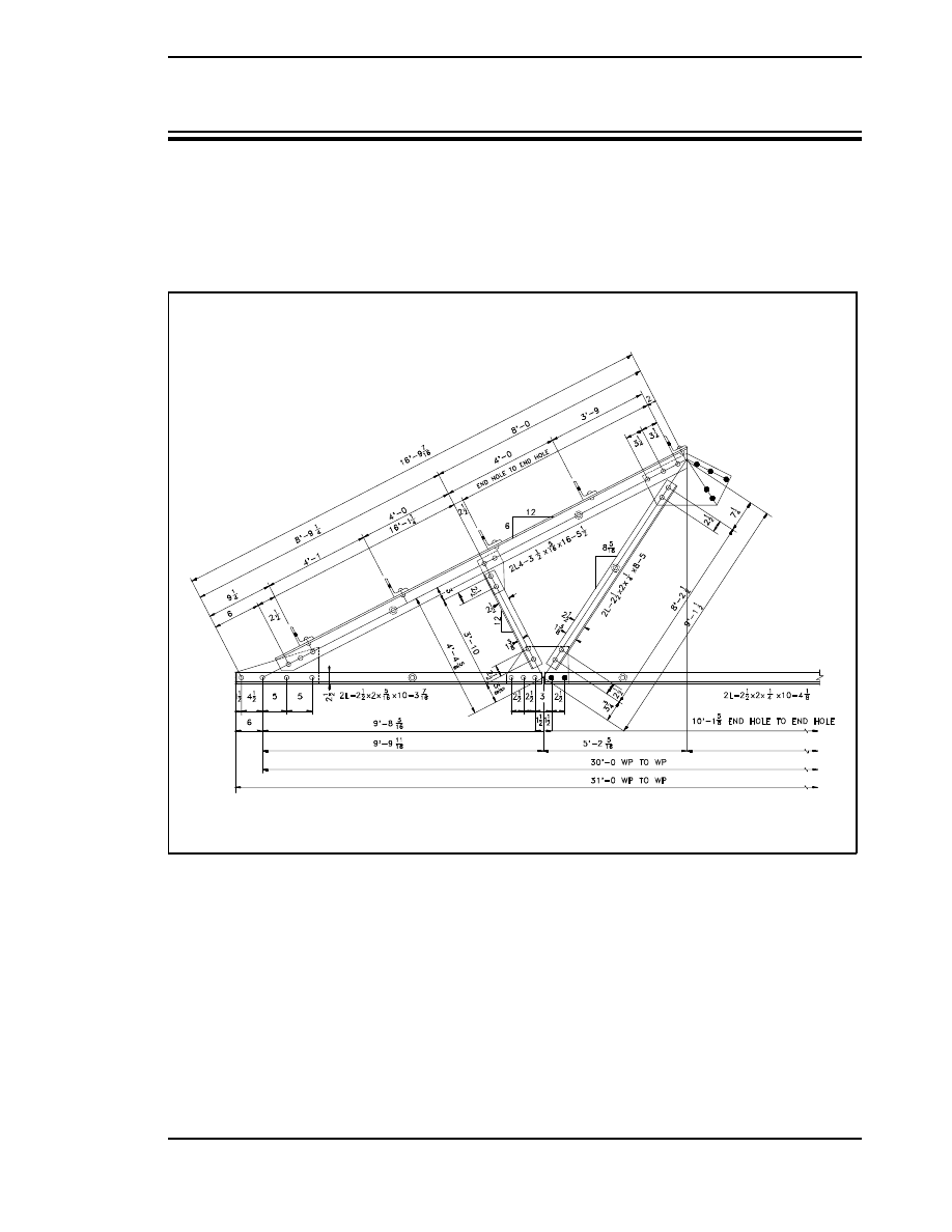
Construction drawings are found principally at sites where the construction of a structure or
system is being performed. These drawings usually depict each structure/system or portion of
a structure/system as an orthographic projection with each view containing the necessary
dimensions required for assembly. Figure 2 provides an example of a construction print for a
section of a steel roof truss.
Architectural drawings are used by architects in the conceptual design of buildings and
structures. These drawings do not provide detailed information on how the structure or
building is to be built, but rather they provide information on how the designer wants the
building to appear and how it will function. Examples of this are location-size-type of doors,
windows, rooms, flow of people, storage areas, and location of equipment. These drawings can
be presented in several formats, including orthographic, isometric, plan, elevation, or
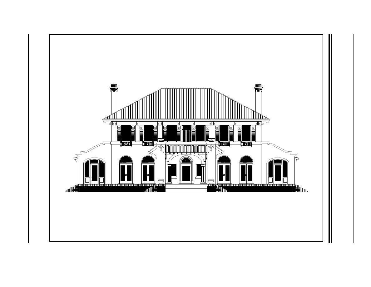
perspective. Figure 3 provides an example of an architectural drawing, of a county library.
DOE-HDBK-1016/2-93
ENGINEERING FABRICATION, CONSTRUCTION,
Engineering Fabrication,
AND ARCHITECTURAL DRAWINGS
Construction, and Architectural Drawings
PR-06
Page 4
Rev. 0

DOE-HDBK-1016/2-93
Engineering Fabrication,
ENGINEERING FABRICATION, CONSTRUCTION,
Construction, and Architectural Drawings
AND ARCHITECTURAL DRAWINGS
Rev. 0
Page 5
PR-06
For any engineering fabrication, construction, or architectural drawing to be of value, exact
information concerning the various dimensions and their tolerances must be provided by the
drawing. Drawings usually denote dimensions and tolerances per the American National
Standards Institute (ANSI) standards. These standards are explained in detail in Dimensioning
and Tolerancing, ANSI Y14.5M - 1982. This section will review the basic methods of denoting
dimensions and tolerances on drawings per the ANSI standards.
Dimensions on a drawing can be expressed in one of two ways. In the first method, the drawing
is drafted to scale and any measurement is obtained by measuring the drawing and correcting for
the scale. In the second method, the actual dimensions of the component are specified on the
drawing. The second method is the preferred method because it reduces the chances of error
and allows greater accuracy and drawing flexibility. Because even the simplest component has
several dimensions that must be stated (and each dimension must have a tolerance), a drawing
can quickly become cluttered with dimensions. To reduce this problem, the ANSI standards
provide rules and conventions for dimensioning a drawing. The basic rules and conventions
must be understood before a dimensioned drawing can be correctly read.

DOE-HDBK-1016/2-93
ENGINEERING FABRICATION, CONSTRUCTION,
Engineering Fabrication,
AND ARCHITECTURAL DRAWINGS
Construction, and Architectural Drawings
PR-06
Page 6
Rev. 0
Figure 4 Types of Dimensioning Lines
Dimensioning and Tolerance Symbology, Rules, and Conventions
When actual dimensions are specified on a print, the basic line symbols that are illustrated by
Figure 4 are used.
DOE-HDBK-1016/2-93
Engineering Fabrication,
ENGINEERING FABRICATION, CONSTRUCTION,
Construction, and Architectural Drawings
AND ARCHITECTURAL DRAWINGS
Rev. 0
Page 7
PR-06
Figure 5 Example of Dimensioning Notation
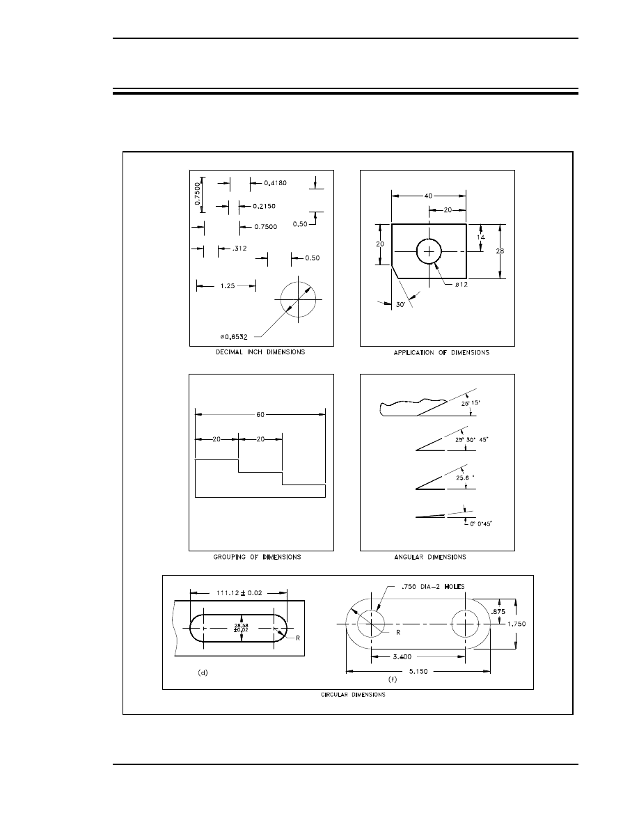
Figure 5 provides examples of the various methods used on drawings to indicate linear, circular
and angular dimensions.

DOE-HDBK-1016/2-93
ENGINEERING FABRICATION, CONSTRUCTION,
Engineering Fabrication,
AND ARCHITECTURAL DRAWINGS
Construction, and Architectural Drawings
PR-06
Page 8
Rev. 0
When a drawing is dimensioned, each dimension must have a tolerance. In many cases, the
tolerance is not stated, but is set to an implied standard. An example is the blueprint for a
house. The measurements are not usually given stated tolerances, but it is implied that the
carpenter will build the building to the normal tolerances of his trade (1/8-1/4 inch), and the
design and use of the blueprints allow for this kind of error. Another method of expressing
tolerances on a drawing is to state in the title block, or in a note, a global tolerance for all
measurements on the drawing.
The last method is to state the tolerance for a specified dimension with the measurement. This
method is usually used in conjunction with one of the other two tolerancing methods. This type
of notation is commonly used for a dimension that requires a higher level of accuracy than the
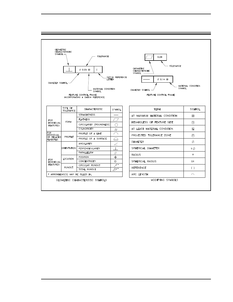
remainder of the drawing. Figure 6 provides several examples of how this type of tolerancing
notation can appear on a drawing.
Tolerances are applied to more than just linear dimensions, such as 1 + 0.1 inches. They can
apply to any dimension, including the radius, the degree of out-of-round, the allowable out-of-
square, the surface condition, or any other parameter that effects the shape and size of the
object. These types of tolerances are called geometric tolerances. Geometric tolerances state
the maximum allowable variation of a form or its position from the perfect geometry implied
on the drawing. The term geometry refers to various forms, such as a plane, a cylinder, a cone,
a square, or a hexagon. Theoretically these are perfect forms, but because it is impossible to
produce perfect forms, it may be necessary to specify the amount of variation permitted. These
tolerances specify either the diameter or the width of a tolerance zone within which a surface
or the axis of a cylinder or a hole must be if the part is to meet the required accuracy for proper
function and fit. The methods of indicating geometric tolerances by means of geometric
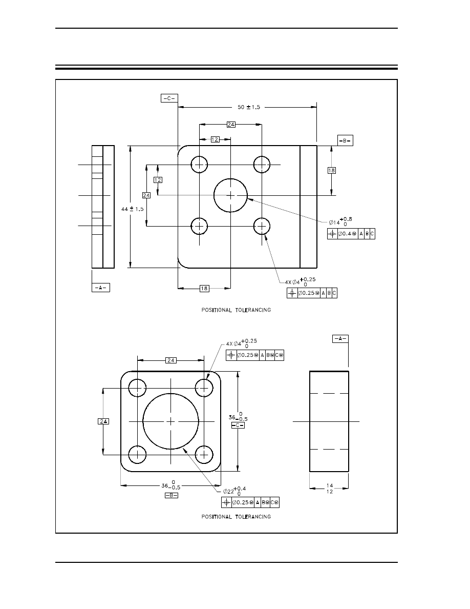
characteristic symbols are shown in Figure 6. Examples of tolerance symbology are shown in
Figure 7.
DOE-HDBK-1016/2-93
Engineering Fabrication,
ENGINEERING FABRICATION, CONSTRUCTION,
Construction, and Architectural Drawings
AND ARCHITECTURAL DRAWINGS
Rev. 0
Page 9
PR-06
DOE-HDBK-1016/2-93
ENGINEERING FABRICATION, CONSTRUCTION,
Engineering Fabrication,
AND ARCHITECTURAL DRAWINGS
Construction, and Architectural Drawings
PR-06
Page 10
Rev. 0
DOE-HDBK-1016/2-93
Engineering Fabrication,
ENGINEERING FABRICATION, CONSTRUCTION,
Construction, and Architectural Drawings
AND ARCHITECTURAL DRAWINGS
Rev. 0
Page 11
PR-06
Figure 8 Example of Tolerancing
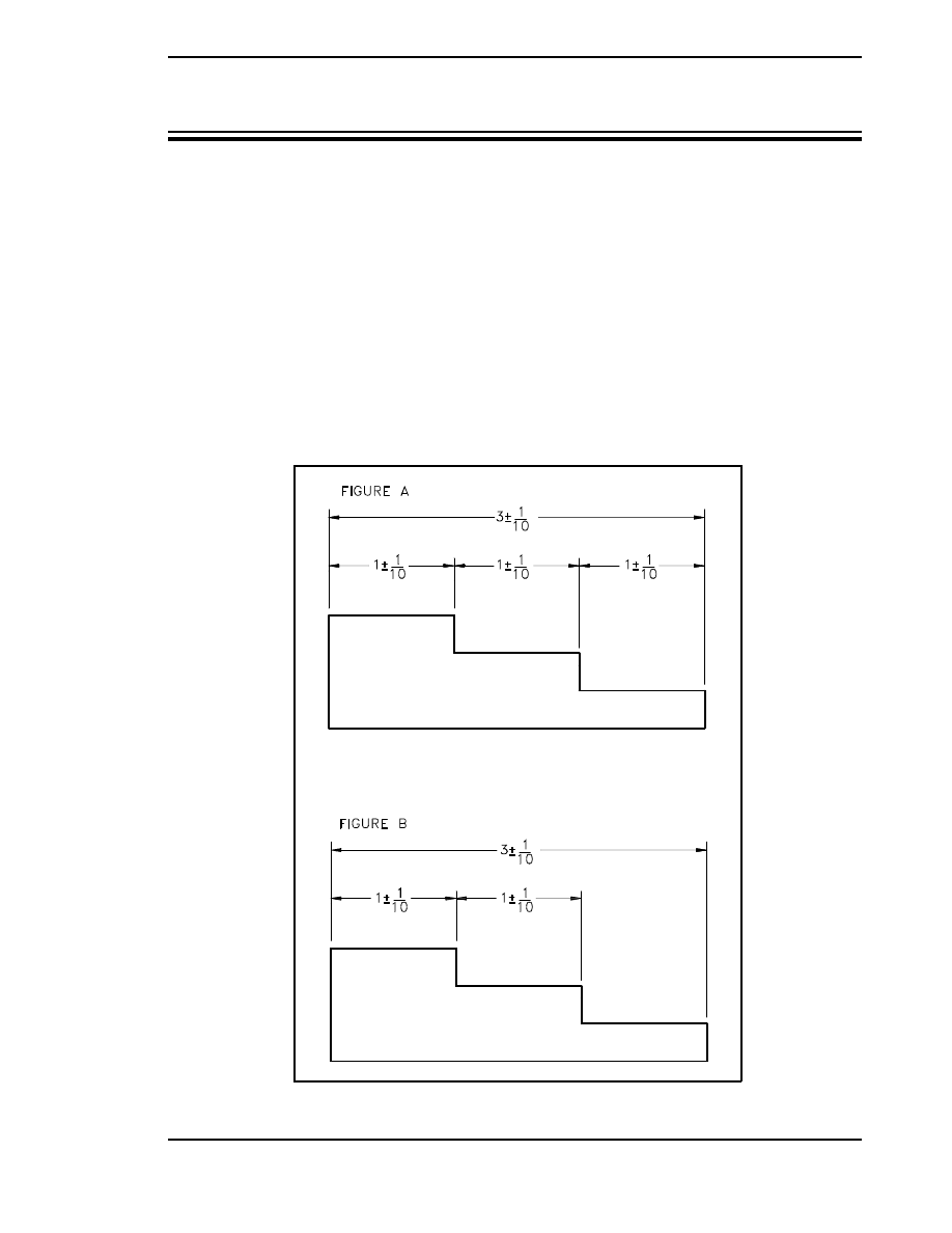
Because tolerances allow a part or the placement of a part or feature to vary or have a range,
all of an object's dimensions can not be specified. This allows the unspecified, and therefor non-
toleranced, dimension to absorb the errors in the critical dimensions. As illustrated in Figure
8 (A) for example, all of the internal dimensions plus each dimension's maximum tolerance adds
up to more than the specified overall dimension and its maximum tolerance. In this case the
length of each step plus its maximum tolerance is 1 1/10 inches, for a maximum object length
of 3 3/10 inches. However the drawing also specifies that the total length of the object cannot
exceed 3 1/10 inches. A drawing dimensioned in this manner is not correct, and one of the
following changes must be made if the part is to be correctly manufactured.
To prevent this type of conflict, the designer must either specify different tolerances for each
of the dimensions so that the length of each smaller dimension plus its maximum error adds up
to a value within the overall dimension plus its tolerance, or leave one of the dimensions off,
as illustrated in Figure 8 (B) (the preferred method).
DOE-HDBK-1016/2-93
ENGINEERING FABRICATION, CONSTRUCTION,
Engineering Fabrication,
AND ARCHITECTURAL DRAWINGS
Construction, and Architectural Drawings
PR-06
Page 12
Rev. 0
Engineering Fabrication, Construction,
and Architectural Drawings Summary
The purpose of a fabrication drawing is to provide the information necessary to
manufacture and machine components.
The purpose of construction drawings is to provide the information necessary to
build and assemble structures and systems.
The purpose of architectural drawings is to provide conceptual information about
buildings and structures.
This chapter reviewed the basic symbology used in dimensioning engineering
fabrication, construction, and architectural drawings.
The important information in this chapter is summarized below.
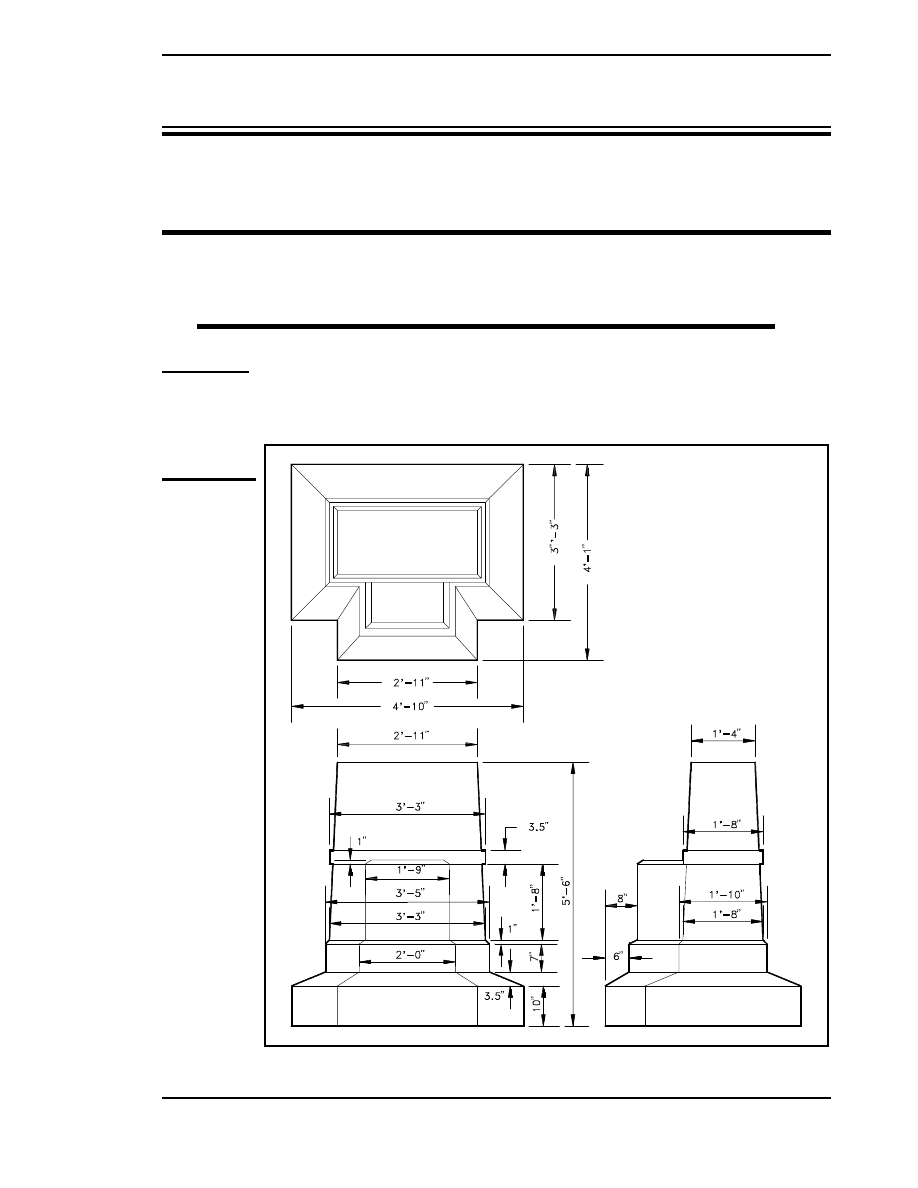
DOE-HDBK-1016/2-93
Engineering Fabrication,
ENGINEERING FABRICATION, CONSTRUCTION,
Construction, and Architectural Drawings
AND ARCHITECTURAL DRAWINGS, EXAMPLES
Rev. 0
Page 13
PR-06
ENGINEERING FABRICATION, CONSTRUCTION,
AND ARCHITECTURAL DRAWING, EXAMPLES
The information presented in the previous chapter is reviewed in this chapter
through the performance of reading drawing examples.
To aid in understanding the material presented in this module, practice reading the following
prints by answering the questions. The answers are on the page following the last example.
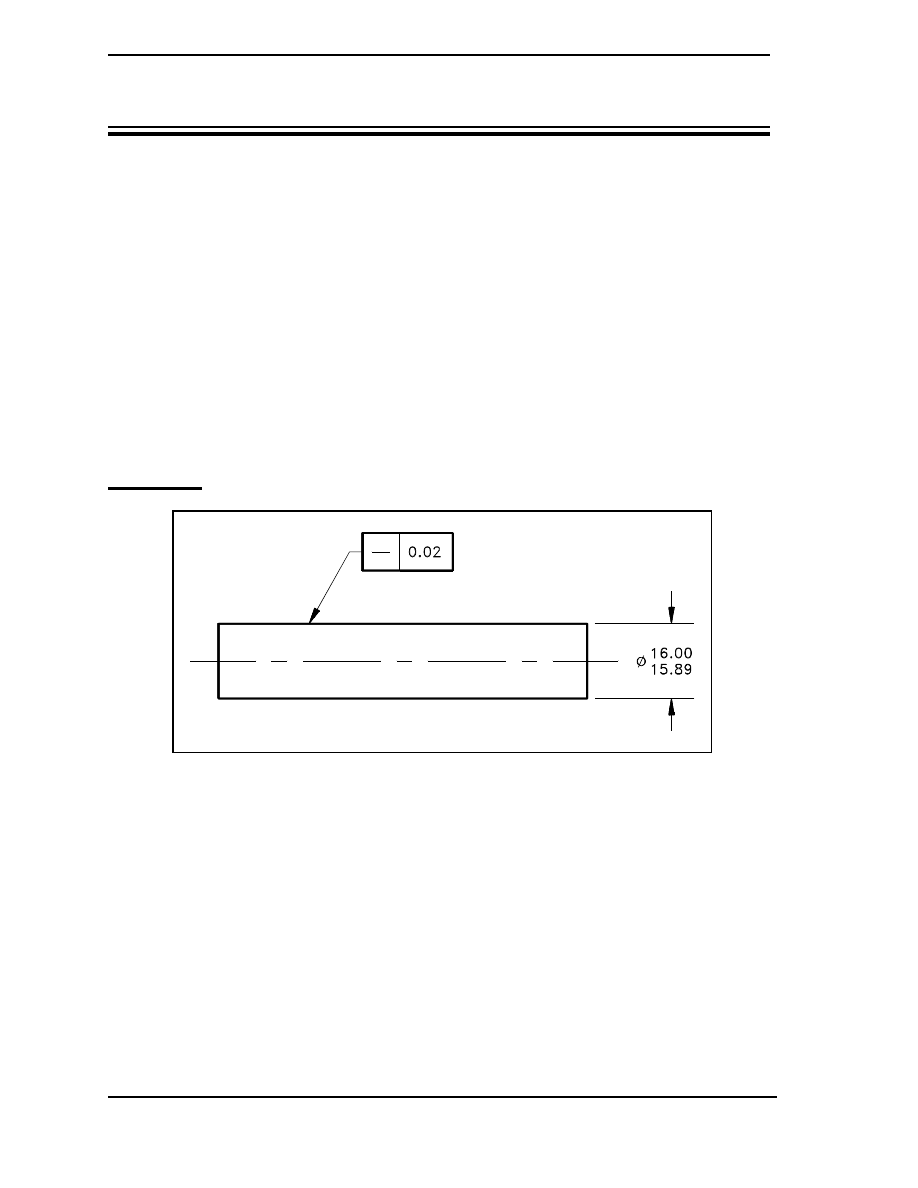
DOE-HDBK-1016/2-93
ENGINEERING FABRICATION, CONSTRUCTION,
Engineering Fabrication,
AND ARCHITECTURAL DRAWINGS, EXAMPLES
Construction, and Architectural Drawings
PR-06
Page 14
Rev. 0
1.
What is the overall height of the structure?
2.
What is the width (front-to-back) of the structure?
3.
What is the difference between the width (front-to-back) and the width (side-to-side) of
the base of the structure?
1.
What is the geometric characteristic being given a tolerance?
2.
What is the maximum diameter of the shaft?
3.
What is the minimum diameter of the shaft?
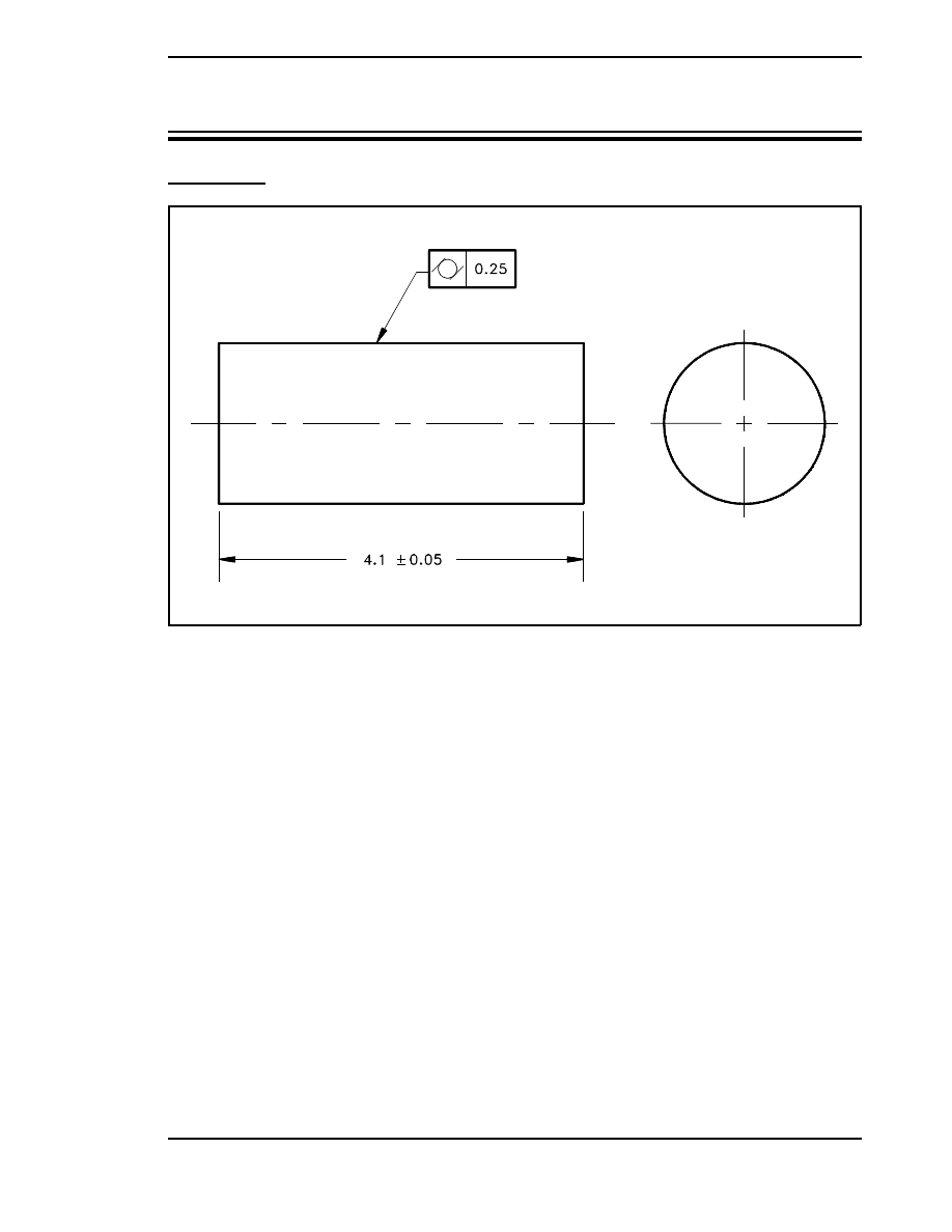
DOE-HDBK-1016/2-93
Engineering Fabrication,
ENGINEERING FABRICATION, CONSTRUCTION,
Construction, and Architectural Drawings
AND ARCHITECTURAL DRAWINGS, EXAMPLES
Rev. 0
Page 15
PR-06
1.
What is the geometric characteristic being given a tolerance?
2.
What is the maximum length of the cylinder?
3.
What is the minimum length of the cylinder?

DOE-HDBK-1016/2-93
ENGINEERING FABRICATION, CONSTRUCTION,
Engineering Fabrication,
AND ARCHITECTURAL DRAWINGS, EXAMPLES
Construction, and Architectural Drawings
PR-06
Page 16
Rev. 0
Answers to example 1.
1.
5' 6"
2.
4' 1"
3.
9" (4' 10" side-to-side distance - 4' 1" front-to-back distance)
Answers to example 2.
1.
Using Figure 6, the straight line in the geometric characteristic box indicates
"straightness." This implies that the surface must be straight to with in 0.02 inches.
2.
16.00 inches
3.
15.89 inches
Answers to example 3.
1.
Using Figure 6, the circle with two parallel bars in the geometric characteristic box
indicates "Cylindricity," or how close to being a perfect cylinder it must be (in this case
0.25 inches).
2.
4.15 inches. The nominal length of 4.1 plus the tolerance of 0.05.
3.
4.05 inches. The nominal length of 4.1 minus the tolerance of 0.05.
DOE-HDBK-1016/2-93
Engineering Fabrication,
ENGINEERING FABRICATION, CONSTRUCTION,
Construction, and Architectural Drawings
AND ARCHITECTURAL DRAWINGS, EXAMPLES
Rev. 0
Page 17
PR-06
Engineering Fabrication, Construction,
and Architectural Drawing Exercise Summary
This chapter reviewed the material on dimensioning and tolerancing
engineering fabrication, construction, and architectural drawings.
The important information in this chapter is summarized below.

DOE-HDBK-1016/2-93
ENGINEERING FABRICATION, CONSTRUCTION,
Engineering Fabrication,
AND ARCHITECTURAL DRAWINGS, EXAMPLES
Construction, and Architectural Drawings
PR-06
Page 18
Rev. 0
end of text.
CONCLUDING MATERIAL
Review activities:
Preparing activity:
DOE - ANL-W, BNL, EG&G Idaho,
DOE - NE-73
EG&G Mound, EG&G Rocky Flats,
Project Number 6910-0022
LLNL, LANL, MMES, ORAU, REECo,
WHC, WINCO, WEMCO, and WSRC.
Document Outline
- ABSTRACT
- FOREWORD
- OVERVIEW
- Module 4 Electronic Diagrams and Schematics
- Module 5 Logic Diagrams
- Module 6 Engineering Fabrication, Construction, and Architectural Drawings
- CONCLUDING MATERIAL
Wyszukiwarka
Podobne podstrony:
Engineering Symbols, Prints and Drawings 01 US DOE
kurs rysowanie basic painting and drawing principles 56R3OH6IXOXH3MLLJUG4HH6IFQRMWM3PU6JGLFI
Keyes, J Gregory Kingdoms of Thorn and Bone 02 The Charnel Prince
Harry Harrison Stars And Stripes 02 Stars And Stripes In Peril v3 0 (lit)
Create Your Own Search Engine with PHP and Google Web Services
Haunted house reading and drawing activity
Complex Numbers and Complex Arithmetic [article] J Doe WW
Nikki and Michael 02 Hearts in Darkness
A Short Guide to Occult Symbols Pentacles and Pentagrams NA4W0302
Greg Costikyan Cups and Sorcery 02 One Quest, Hold the Dragons
Texas Hold em Opening Hands And Drawing Odds (Matthew Hilger)
[Engineering] Electrical Power and Energy Systems 1999 21 Dynamics Of Diesel And Wind Turbine Gene
Diana Palmer Rawhide and Lace 02 Unlikely Lover
Fundamentals of Anatomy and Physiology 02 Chapter
Exercise symbols customs and traditions of Christmas KEY
Forgotten Realms Counselors and Kings 02 The Floodgate
Agatha Christie Tommy and Tuppence 02 Partners In Crime
Alexandra Ivy Abandoned and Unseen 02 (Branded Packs)
Palmer Diana Rawhide and Lace 02 Deszczowa piosenka (Gwiazdy Romansu)
więcej podobnych podstron
