ARM7TDMI Data Sheet
ARM DDI 0029E
4-1
11
1
Open Access
ARM Instruction Set
This chapter describes the ARM instruction set.
4.1
Instruction Set Summary
4-2
4.2
The Condition Field
4-5
4.3
Branch and Exchange (BX)
4-6
4.4
Branch and Branch with Link (B, BL)
4-8
4.5
Data Processing
4-10
4.6
PSR Transfer (MRS, MSR)
4-18
4.7
Multiply and Multiply-Accumulate (MUL, MLA)
4-23
4.8
Multiply Long and Multiply-Accumulate Long (MULL,MLAL)
4-25
4.9
Single Data Transfer (LDR, STR)
4-28
4.10
Halfword and Signed Data Transfer
4-34
4.11
Block Data Transfer (LDM, STM)
4-40
4.12
Single Data Swap (SWP)
4-47
4.13
Software Interrupt (SWI)
4-49
4.14
Coprocessor Data Operations (CDP)
4-51
4.15
Coprocessor Data Transfers (LDC, STC)
4-53
4.16
Coprocessor Register Transfers (MRC, MCR)
4-57
4.17
Undefined Instruction
4-60
4.18
Instruction Set Examples
4-61
4
ARM Instruction Set - Summary
ARM7TDMI Data Sheet
ARM DDI 0029E
4-2
Open Access
4.1
Instruction Set Summary
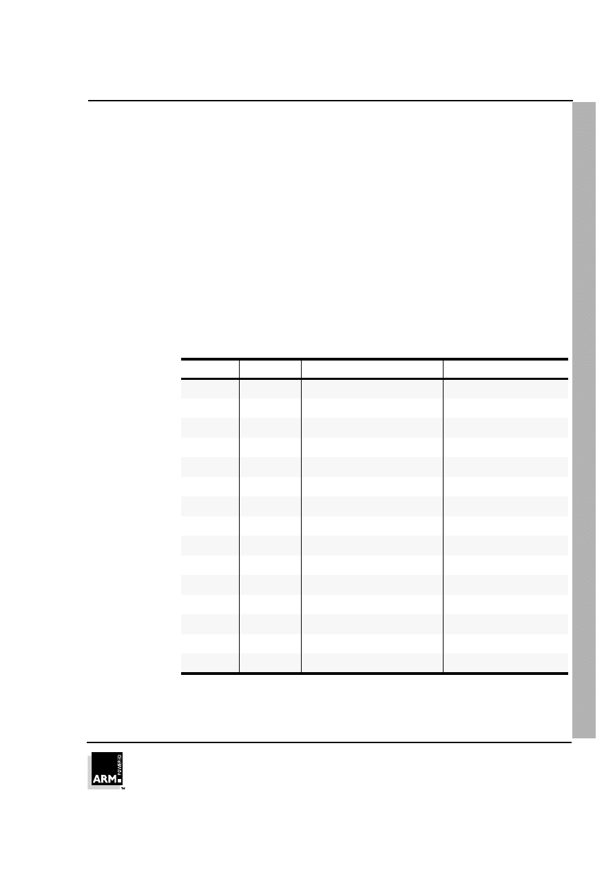
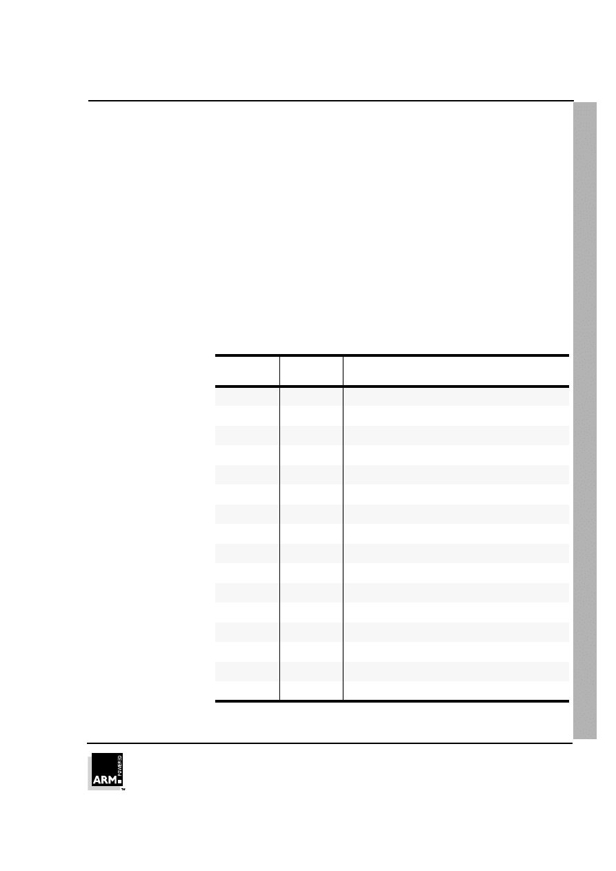
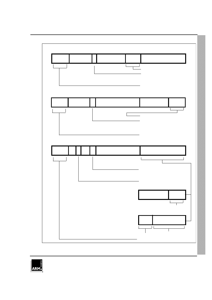
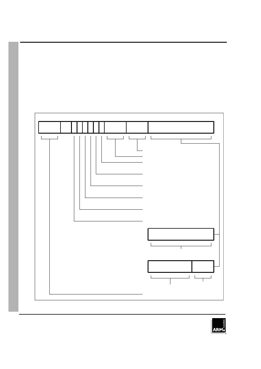
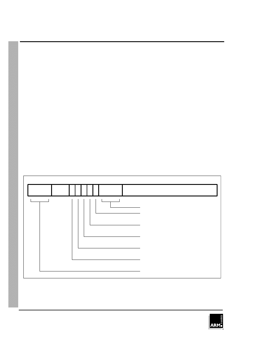
4.1.1 Format summary
The ARM instruction set formats are shown below.
Figure 4-1: ARM instruction set formats
Note
Some instruction codes are not defined but do not cause the Undefined instruction trap
to be taken, for instance a Multiply instruction with bit 6 changed to a 1. These
instructions should not be used, as their action may change in future ARM
implementations.
31 30 29 28 27 26 25 24 23 22 21 20 19 18 17 16 15 14 13 12 11 10 9
8
7
6
5
4
3
2
1
0
Cond
0 0 I
Opcode
S
Rn
Rd
Operand 2
Data Processing /
PSR Transfer
Cond
0 0 0 0 0 0 A S
Rd
Rn
Rs
1 0 0 1
Rm
Multiply
Cond
0 0 0 0 1 U A S
RdHi
RdLo
Rn
1 0 0 1
Rm
Multiply Long
Cond
0 0 0 1 0 B 0 0
Rn
Rd
0 0 0 0 1 0 0 1
Rm
Single Data Swap
Cond
0 0 0 1 0 0 1 0 1 1 1 1 1 1 1 1 1 1 1 1 0 0 0 1
Rn
Branch and Exchange
Cond
0 0 0 P U 0 W L
Rn
Rd
0 0 0 0 1 S H 1
Rm
Halfword Data Transfer:
register offset
Cond
0 0 0 P U 1 W L
Rn
Rd
Offset 1 S H 1
Offset
Halfword Data Transfer:
immediate offset
Cond
0 1 I P U B W L
Rn
Rd
Offset
Single Data Transfer
Cond
0 1 1
1
Undefined
Cond
1 0 0 P U S W L
Rn
Register List
Block Data Transfer
Cond
1 0 1 L
Offset
Branch
Cond
1 1 0 P U N W L
Rn
CRd
CP#
Offset
Coprocessor Data
Transfer
Cond
1 1 1 0
CP Opc
CRn
CRd
CP#
CP
0
CRm
Coprocessor Data
Operation
Cond
1 1 1 0 CP Opc L
CRn
Rd
CP#
CP
1
CRm
Coprocessor Register
Transfer
Cond
1 1 1 1
Ignored by processor
Software Interrupt
31 30 29 28 27 26 25 24 23 22 21 20 19 18 17 16 15 14 13 12 11 10 9
8
7
6
5
4
3
2
1
0
ARM Instruction Set - Summary
ARM7TDMI Data Sheet
ARM DDI 0029E
4-3
Open Access
4.1.2 Instruction summary
Mnemonic
Instruction
Action
See Section:
ADC
Add with carry
Rd := Rn + Op2 + Carry
4.5
ADD
Add
Rd := Rn + Op2
4.5
AND
AND
Rd := Rn AND Op2
4.5
B
Branch
R15 := address
4.4
BIC
Bit Clear
Rd := Rn AND NOT Op2
4.5
BL
Branch with Link
R14 := R15, R15 := address
4.4
BX
Branch and Exchange
R15 := Rn,
T bit := Rn[0]
4.3
CDP
Coprocesor Data Processing
(Coprocessor-specific)
4.14
CMN
Compare Negative
CPSR flags := Rn + Op2
4.5
CMP
Compare
CPSR flags := Rn - Op2
4.5
EOR
Exclusive OR
Rd := (Rn AND NOT Op2)
OR (op2 AND NOT Rn)
4.5
LDC
Load coprocessor from
memory
Coprocessor load
4.15
LDM
Load multiple registers
Stack manipulation (Pop)
4.11
LDR
Load register from memory
Rd := (address)
4.9, 4.10
MCR
Move CPU register to
coprocessor register
cRn := rRn {<op>cRm}
4.16
MLA
Multiply Accumulate
Rd := (Rm * Rs) + Rn
4.7, 4.8
MOV
Move register or constant
Rd : = Op2
4.5
MRC
Move from coprocessor
register to CPU register
Rn := cRn {<op>cRm}
4.16
MRS
Move PSR status/flags to
register
Rn := PSR
4.6
MSR
Move register to PSR
status/flags
PSR := Rm
4.6
MUL
Multiply
Rd := Rm * Rs
4.7, 4.8
MVN
Move negative register
Rd := 0xFFFFFFFF EOR Op2
4.5
ORR
OR
Rd := Rn OR Op2
4.5
Table 4-1: The ARM Instruction set
ARM Instruction Set - Summary
ARM7TDMI Data Sheet
ARM DDI 0029E
4-4
Open Access
RSB
Reverse Subtract
Rd := Op2 - Rn
4.5
RSC
Reverse Subtract with Carry
Rd := Op2 - Rn - 1 + Carry
4.5
SBC
Subtract with Carry
Rd := Rn - Op2 - 1 + Carry
4.5
STC
Store coprocessor register to
memory
address := CRn
4.15
STM
Store Multiple
Stack manipulation (Push)
4.11
STR
Store register to memory
<address> := Rd
4.9, 4.10
SUB
Subtract
Rd := Rn - Op2
4.5
SWI
Software Interrupt
OS call
4.13
SWP
Swap register with memory
Rd := [Rn], [Rn] := Rm
4.12
TEQ
Test bitwise equality
CPSR flags := Rn EOR Op2
4.5
TST
Test bits
CPSR flags := Rn AND Op2
4.5
Mnemonic
Instruction
Action
See Section:
Table 4-1: The ARM Instruction set (Continued)
ARM Instruction Set - Condition Field
ARM7TDMI Data Sheet
ARM DDI 0029E
4-5
Open Access
4.2
The Condition Field
In ARM state, all instructions are conditionally executed according to the state of the
CPSR condition codes and the instruction’s condition field. This field (bits 31:28)
determines the circumstances under which an instruction is to be executed. If the state
of the C, N, Z and V flags fulfils the conditions encoded by the field, the instruction is
executed, otherwise it is ignored.
There are sixteen possible conditions, each represented by a two-character suffix that
can be appended to the instruction’s mnemonic. For example, a Branch (
B
in assembly
language) becomes
BEQ
for "Branch if Equal", which means the Branch will only be
taken if the Z flag is set.
In practice, fifteen different conditions may be used: these are listed in
➲
Table 4-2:
Condition code summary. The sixteenth (1111) is reserved, and must not be used.
In the absence of a suffix, the condition field of most instructions is set to "Always"
(sufix AL). This means the instruction will always be executed regardless of the CPSR
condition codes.
Code
Suffix
Flags
Meaning
0000
EQ
Z set
equal
0001
NE
Z clear
not equal
0010
CS
C set
unsigned higher or same
0011
CC
C clear
unsigned lower
0100
MI
N set
negative
0101
PL
N clear
positive or zero
0110
VS
V set
overflow
0111
VC
V clear
no overflow
1000
HI
C set and Z clear
unsigned higher
1001
LS
C clear or Z set
unsigned lower or same
1010
GE
N equals V
greater or equal
1011
LT
N not equal to V
less than
1100
GT
Z clear AND (N equals V)
greater than
1101
LE
Z set OR (N not equal to V)
less than or equal
1110
AL
(ignored)
always
Table 4-2: Condition code summary
ARM Instruction Set - Condition Field
ARM7TDMI Data Sheet
ARM DDI 0029E
4-6
Open Access
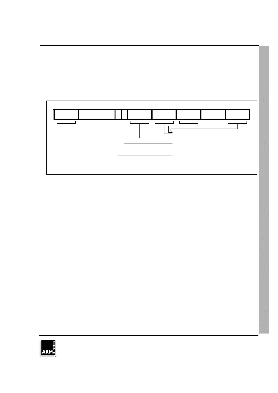
4.3
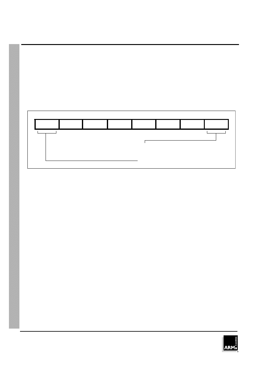
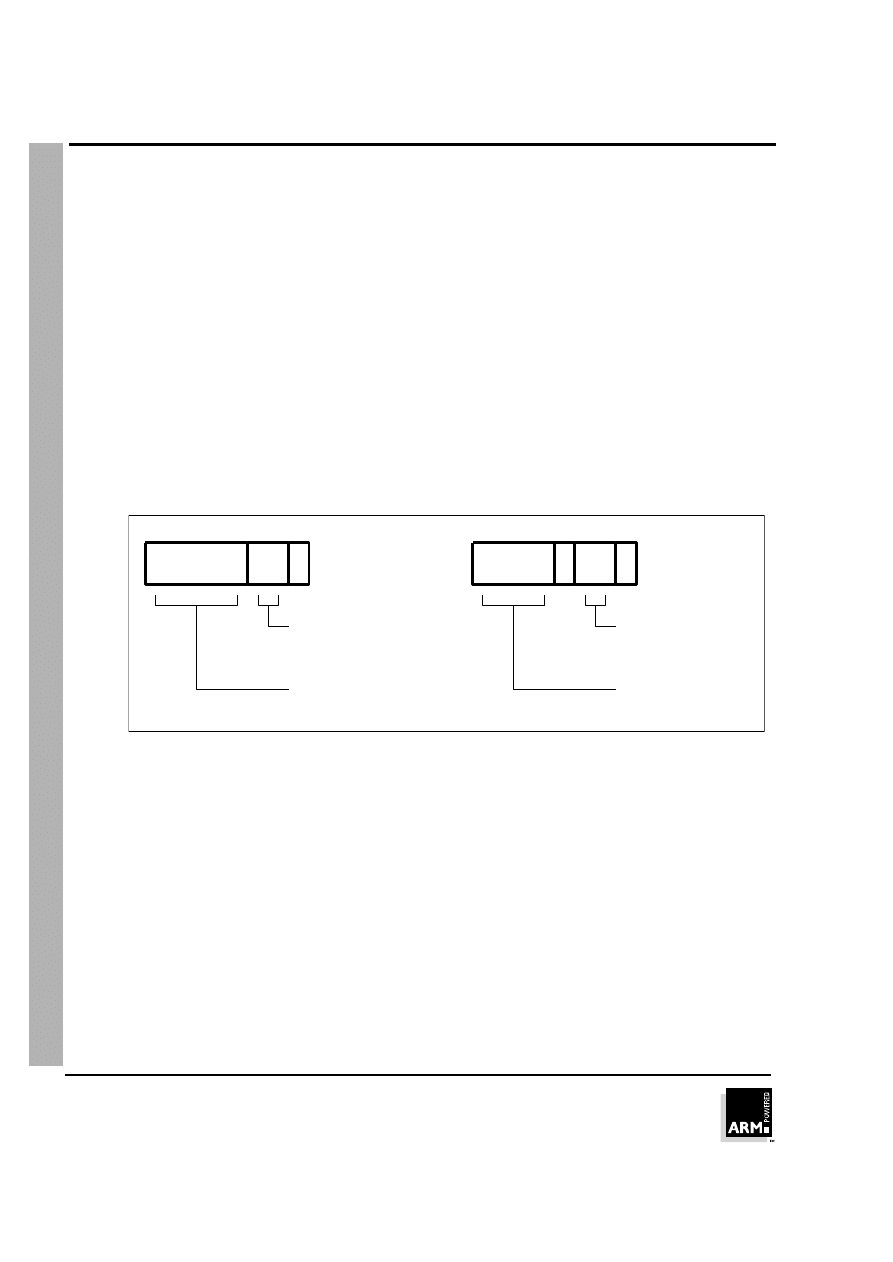
Branch and Exchange (BX)
This instruction is only executed if the condition is true. The various conditions are
defined in
➲
Table 4-2: Condition code summary on page 4-5.
This instruction performs a branch by copying the contents of a general register, Rn,
into the program counter, PC. The branch causes a pipeline flush and refill from the
address specified by Rn. This instruction also permits the instruction set to be
exchanged. When the instruction is executed, the value of Rn[0] determines whether
the instruction stream will be decoded as ARM or THUMB instructions.
Figure 4-2: Branch and Exchange instructions
4.3.1 Instruction cycle times
The BX instruction takes 2S + 1N cycles to execute, where S and N are as defined in
➲
6.2 Cycle Types on page 6-2.
4.3.2 Assembler syntax
BX - branch and exchange.
BX{cond} Rn
{cond}
Two character condition mnemonic. See
➲
Table 4-2: Condition code
summary on page 4-5.
Rn
is an expression evaluating to a valid register number.
4.3.3 Using R15 as an operand
If R15 is used as an operand, the behaviour is undefined.
Cond
0 0 0 1 0 0 1 0
0
0 0
1
Rn
0
3
4
7
8
11
12
15
16
19
20
23
24
27
28
31
Operand register
If bit 0 of Rn = 1, subsequent instructions decoded as THUMB instructions
If bit 0 of Rn = 0, subsequent instructions decoded as ARM instructions
Condition Field
1 1 1 1
1 1 1 1
1 1 1 1

ARM Instruction Set - Condition Field
ARM7TDMI Data Sheet
ARM DDI 0029E
4-7
Open Access
4.3.4 Examples
ADR R0, Into_THUMB + 1
; Generate branch target address
; and set bit 0 high - hence
; arrive in THUMB state.
BX R0
; Branch and change to THUMB
; state.
CODE16
; Assemble subsequent code as
Into_THUMB
; THUMB instructions
.
.
ADR R5, Back_to_ARM
: Generate branch target to word
: aligned ; address - hence bit 0
; is low and so change back to ARM
; state.
BX R5
; Branch and change back to ARM
; state.
.
.
ALIGN
; Word align
CODE32
; Assemble subsequent code as ARM
Back_to_ARM
; instructions
.
.
ARM Instruction Set - B, BL
ARM7TDMI Data Sheet
ARM DDI 0029E
4-8
Open Access
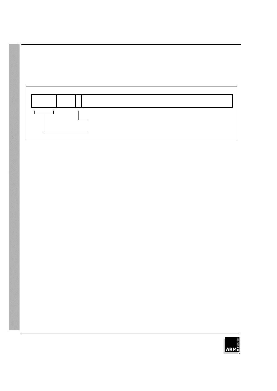
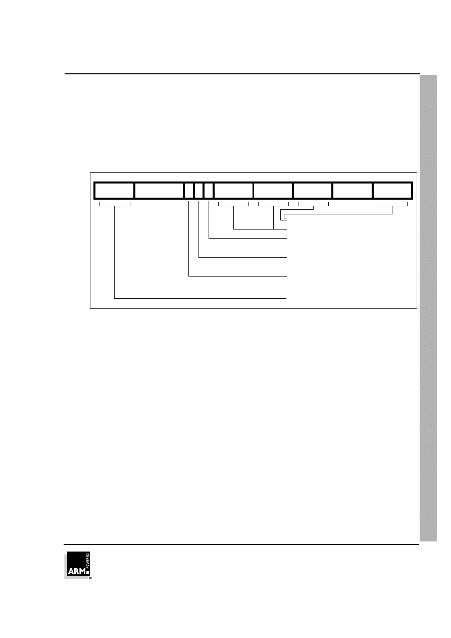
4.4
Branch and Branch with Link (B, BL)
The instruction is only executed if the condition is true. The various conditions are
defined
➲
Table 4-2: Condition code summary on page 4-5. The instruction encoding
is shown in
➲
Figure 4-3: Branch instructions, below.
Figure 4-3: Branch instructions
Branch instructions contain a signed 2's complement 24 bit offset. This is shifted left
two bits, sign extended to 32 bits, and added to the PC. The instruction can therefore
specify a branch of +/- 32Mbytes. The branch offset must take account of the prefetch
operation, which causes the PC to be 2 words (8 bytes) ahead of the current
instruction.
Branches beyond +/- 32Mbytes must use an offset or absolute destination which has
been previously loaded into a register. In this case the PC should be manually saved
in R14 if a Branch with Link type operation is required.
4.4.1 The link bit
Branch with Link (BL) writes the old PC into the link register (R14) of the current bank.
The PC value written into R14 is adjusted to allow for the prefetch, and contains the
address of the instruction following the branch and link instruction. Note that the CPSR
is not saved with the PC and R14[1:0] are always cleared.
To return from a routine called by Branch with Link use MOV PC,R14 if the link register
is still valid or LDM Rn!,{..PC} if the link register has been saved onto a stack pointed
to by Rn.
4.4.2 Instruction cycle times
Branch and Branch with Link instructions take 2S + 1N incremental cycles, where S
and N are as defined in
➲
6.2 Cycle Types on page 6-2.
Cond
101
L
offset
31
28 27
25 24 23
0
Link bit
0 = Branch
1 = Branch with Link
Condition field

ARM Instruction Set - B, BL
ARM7TDMI Data Sheet
ARM DDI 0029E
4-9
Open Access
4.4.3 Assembler syntax
Items in {} are optional. Items in <> must be present.
B{L}{cond} <expression>
{L}
is used to request the Branch with Link form of the instruction.
If absent, R14 will not be affected by the instruction.
{cond}
is a two-character mnemonic as shown in
➲
Table 4-2:
Condition code summary on page 4-5. If absent then AL
(ALways) will be used.
<expression>
is the destination. The assembler calculates the offset.
4.4.4 Examples
here
BAL
here
; assembles to 0xEAFFFFFE (note effect of
; PC offset).
B
there
; Always condition used as default.
CMP
R1,#0
; Compare R1 with zero and branch to fred
; if R1 was zero, otherwise continue
BEQ
fred
; continue to next instruction.
BL
sub+ROM
; Call subroutine at computed address.
ADDS
R1,#1
; Add 1 to register 1, setting CPSR flags
; on the result then call subroutine if
BLCC
sub
; the C flag is clear, which will be the
; case unless R1 held 0xFFFFFFFF.
ARM Instruction Set - Data processing
ARM7TDMI Data Sheet
ARM DDI 0029E
4-10
Open Access
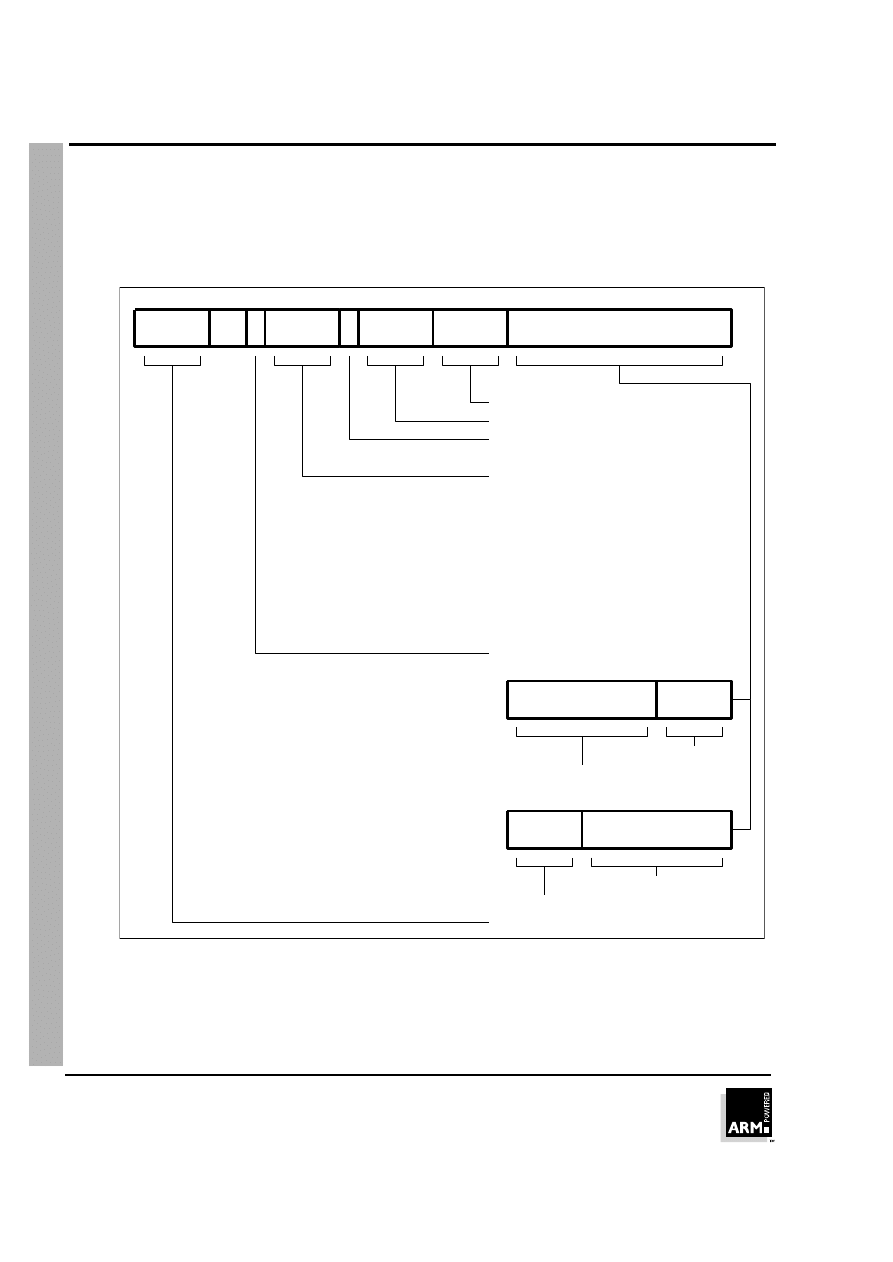
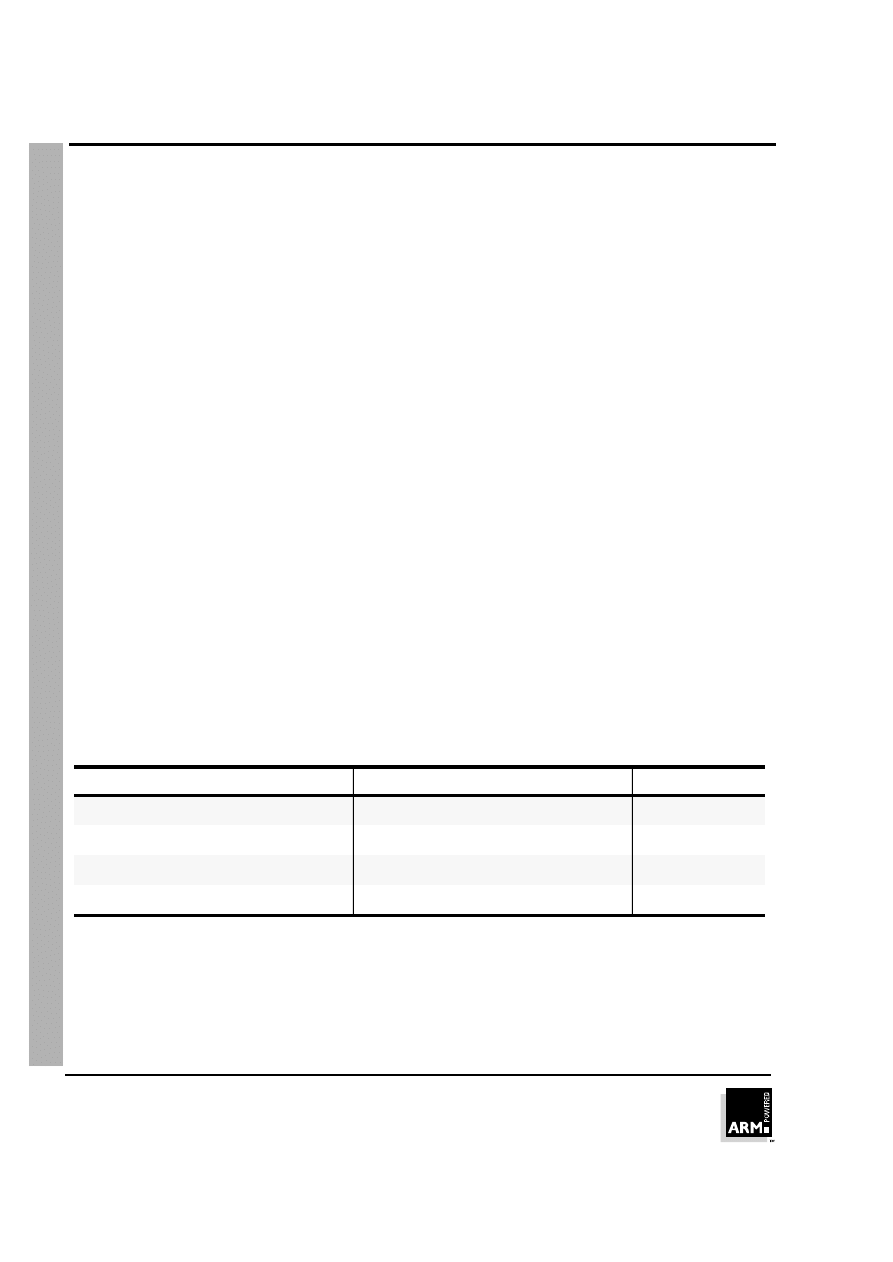
4.5
Data Processing
The data processing instruction is only executed if the condition is true. The conditions
are defined in
➲
Table 4-2: Condition code summary on page 4-5.
The instruction encoding is shown in
➲
Figure 4-4: Data processing instructions below.
Figure 4-4: Data processing instructions
The instruction produces a result by performing a specified arithmetic or logical
operation on one or two operands. The first operand is always a register (Rn).
Cond
00
I
OpCode
Rn
Rd
Operand 2
0
11
12
15
16
19
20
21
24
25
26
27
28
31
Destination register
1st operand register
Set condition codes
Operation Code
0 = do not alter condition codes
1 = set condition codes
0000 = AND - Rd:= Op1 AND Op2
0010 = SUB - Rd:= Op1 - Op2
0011 = RSB - Rd:= Op2 - Op1
0100 = ADD - Rd:= Op1 + Op2
0101 = ADC - Rd:= Op1 + Op2 + C
0110 = SBC - Rd:= Op1 - Op2 + C
0111 = RSC - Rd:= Op2 - Op1 + C
1000 = TST - set condition codes on Op1 AND Op2
1001 = TEQ - set condition codes on Op1 EOR Op2
1010 = CMP - set condition codes on Op1 - Op2
1011 = CMN - set condition codes on Op1 + Op2
1100 = ORR - Rd:= Op1 OR Op2
1101 = MOV - Rd:= Op2
1110 = BIC - Rd:= Op1 AND NOT Op2
1111 = MVN - Rd:= NOT Op2
Immediate Operand
0 = operand 2 is a register
1 = operand 2 is an immediate value
Shift
Rm
Rotate
S
Unsigned 8 bit immediate value
2nd operand register
shift applied to Rm
shift applied to Imm
Imm
Condition field
11
8
7
0
0
3
4
11
0001 = EOR - Rd:= Op1 EOR Op2
- 1
- 1
ARM Instruction Set - Data processing
ARM7TDMI Data Sheet
ARM DDI 0029E
4-11
Open Access
The second operand may be a shifted register (Rm) or a rotated 8 bit immediate value
(Imm) according to the value of the I bit in the instruction. The condition codes in the
CPSR may be preserved or updated as a result of this instruction, according to the
value of the S bit in the instruction.
Certain operations (TST, TEQ, CMP, CMN) do not write the result to Rd. They are used
only to perform tests and to set the condition codes on the result and always have the
S bit set. The instructions and their effects are listed in
➲
Table 4-3: ARM Data
processing instructions on page 4-11.
4.5.1 CPSR flags
The data processing operations may be classified as logical or arithmetic. The logical
operations (AND, EOR, TST, TEQ, ORR, MOV, BIC, MVN) perform the logical action
on all corresponding bits of the operand or operands to produce the result. If the S bit
is set (and Rd is not R15, see below) the V flag in the CPSR will be unaffected, the C
flag will be set to the carry out from the barrel shifter (or preserved when the shift
operation is LSL #0), the Z flag will be set if and only if the result is all zeros, and the
N flag will be set to the logical value of bit 31 of the result
.
Assembler
Mnemonic
OpCode
Action
AND
0000
operand1 AND operand2
EOR
0001
operand1 EOR operand2
SUB
0010
operand1 - operand2
RSB
0011
operand2 - operand1
ADD
0100
operand1 + operand2
ADC
0101
operand1 + operand2 + carry
SBC
0110
operand1 - operand2 + carry - 1
RSC
0111
operand2 - operand1 + carry - 1
TST
1000
as AND, but result is not written
TEQ
1001
as EOR, but result is not written
CMP
1010
as SUB, but result is not written
CMN
1011
as ADD, but result is not written
ORR
1100
operand1 OR operand2
MOV
1101
operand2
(operand1 is ignored)
BIC
1110
operand1 AND NOT operand2
(Bit clear)
MVN
1111
NOT operand2
(operand1 is ignored)
Table 4-3: ARM Data processing instructions
ARM Instruction Set - Shifts
ARM7TDMI Data Sheet
ARM DDI 0029E
4-12
Open Access
The arithmetic operations (SUB, RSB, ADD, ADC, SBC, RSC, CMP, CMN) treat each
operand as a 32 bit integer (either unsigned or 2's complement signed, the two are
equivalent). If the S bit is set (and Rd is not R15) the V flag in the CPSR will be set if
an overflow occurs into bit 31 of the result; this may be ignored if the operands were
considered unsigned, but warns of a possible error if the operands were 2's
complement signed. The C flag will be set to the carry out of bit 31 of the ALU, the Z
flag will be set if and only if the result was zero, and the N flag will be set to the value
of bit 31 of the result (indicating a negative result if the operands are considered to be
2's complement signed).
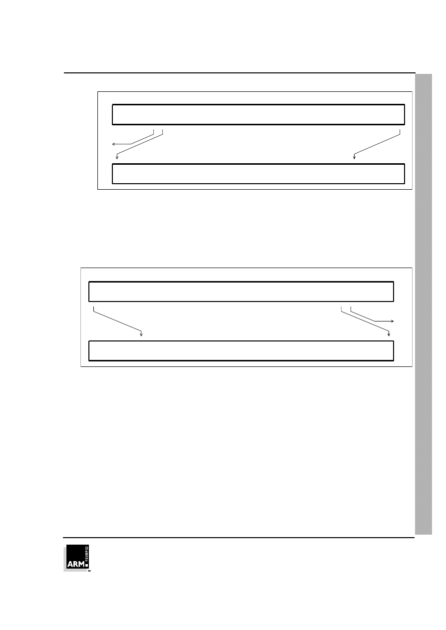
4.5.2 Shifts
When the second operand is specified to be a shifted register, the operation of the
barrel shifter is controlled by the Shift field in the instruction. This field indicates the
type of shift to be performed (logical left or right, arithmetic right or rotate right). The
amount by which the register should be shifted may be contained in an immediate field
in the instruction, or in the bottom byte of another register (other than R15). The
encoding for the different shift types is shown in
➲
Figure 4-5: ARM shift operations.
Figure 4-5: ARM shift operations
Instruction specified shift amount
When the shift amount is specified in the instruction, it is contained in a 5 bit field which
may take any value from 0 to 31. A logical shift left (LSL) takes the contents of Rm and
moves each bit by the specified amount to a more significant position. The least
significant bits of the result are filled with zeros, and the high bits of Rm which do not
map into the result are discarded, except that the least significant discarded bit
becomes the shifter carry output which may be latched into the C bit of the CPSR when
the ALU operation is in the logical class (see above). For example, the effect of LSL #5
is shown in
➲
Figure 4-6: Logical shift left.
0
0
1
Rs
11
8
7
6
5
4
11
7 6
5
4
Shift type
Shift amount
5 bit unsigned integer
00 = logical left
01 = logical right
10 = arithmetic right
11 = rotate right
Shift type
Shift register
00 = logical left
01 = logical right
10 = arithmetic right
11 = rotate right
Shift amount specified in
bottom byte of Rs
ARM Instruction Set - Shifts
ARM7TDMI Data Sheet
ARM DDI 0029E
4-13
Open Access
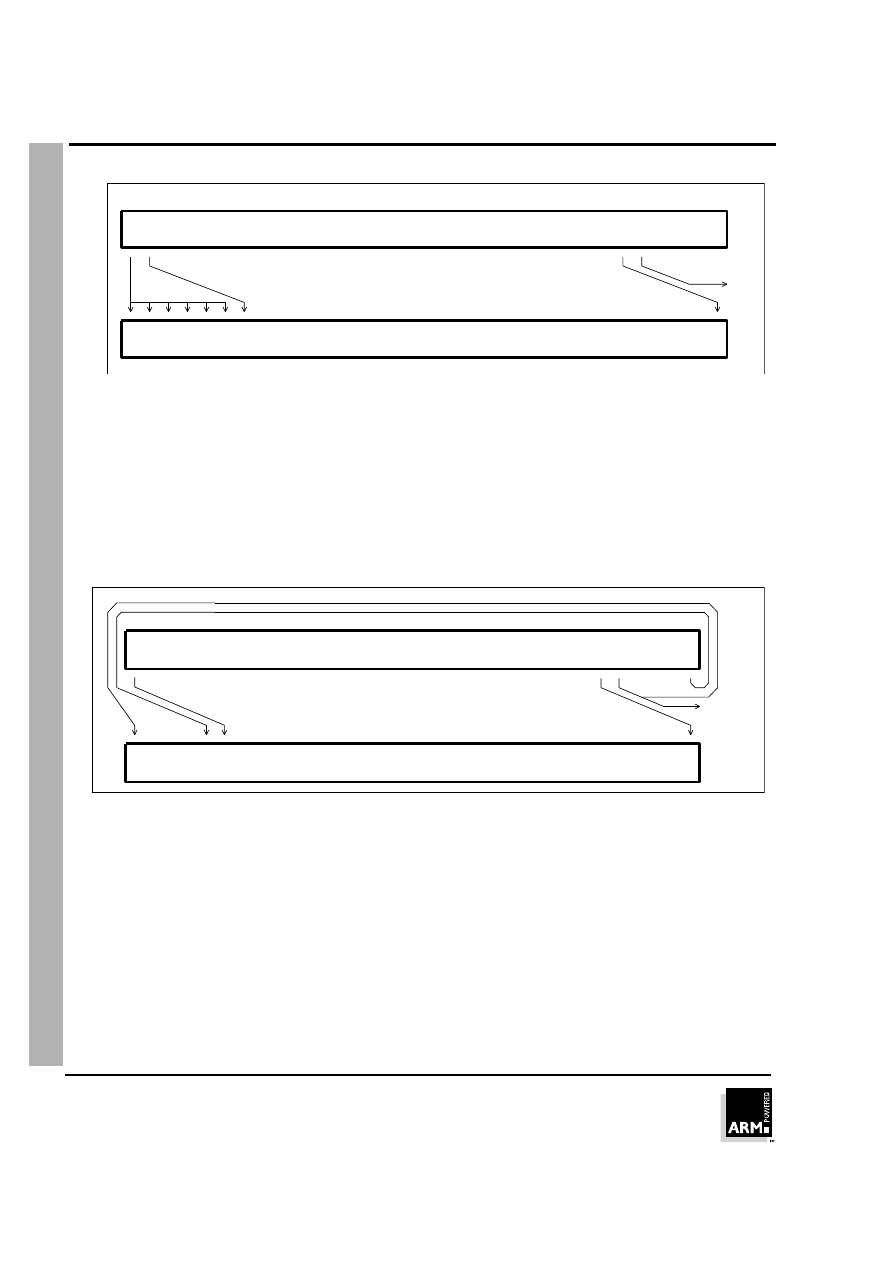
Figure 4-6: Logical shift left
Note
LSL #0 is a special case, where the shifter carry out is the old value of the CPSR C
flag. The contents of Rm are used directly as the second operand.
A logical shift right (LSR) is similar, but the contents of Rm are moved to less
significant positions in the result. LSR #5 has the effect shown in
➲
Figure 4-7: Logical
shift right.
Figure 4-7: Logical shift right
The form of the shift field which might be expected to correspond to LSR #0 is used to
encode LSR #32, which has a zero result with bit 31 of Rm as the carry output. Logical
shift right zero is redundant as it is the same as logical shift left zero, so the assembler
will convert LSR #0 (and ASR #0 and ROR #0) into LSL #0, and allow LSR #32 to be
specified.
An arithmetic shift right (ASR) is similar to logical shift right, except that the high bits
are filled with bit 31 of Rm instead of zeros. This preserves the sign in 2's complement
notation. For example, ASR #5 is shown in
➲
Figure 4-8: Arithmetic shift right.
0 0 0 0 0
contents of Rm
value of operand 2
31
27 26
0
carry out
contents of Rm
value of operand 2
31
0
carry out
0 0 0 0 0
5
4
ARM Instruction Set - Shifts
ARM7TDMI Data Sheet
ARM DDI 0029E
4-14
Open Access
Figure 4-8: Arithmetic shift right
The form of the shift field which might be expected to give ASR #0 is used to encode
ASR #32. Bit 31 of Rm is again used as the carry output, and each bit of operand 2 is
also equal to bit 31 of Rm. The result is therefore all ones or all zeros, according to the
value of bit 31 of Rm.
Rotate right (ROR) operations reuse the bits which “overshoot” in a logical shift right
operation by reintroducing them at the high end of the result, in place of the zeros used
to fill the high end in logical right operations. For example, ROR #5 is shown in
➲
Figure
4-9: Rotate right on page 4-14.
Figure 4-9: Rotate right
The form of the shift field which might be expected to give ROR #0 is used to encode
a special function of the barrel shifter, rotate right extended (RRX). This is a rotate right
by one bit position of the 33 bit quantity formed by appending the CPSR C flag to the
most significant end of the contents of Rm as shown in
➲
Figure 4-10: Rotate right
extended.
contents of Rm
value of operand 2
31
0
carry out
5
4
30
contents of Rm
value of operand 2
31
0
carry out
5 4

ARM Instruction Set - Shifts
ARM7TDMI Data Sheet
ARM DDI 0029E
4-15
Open Access
Figure 4-10: Rotate right extended
Register specified shift amount
Only the least significant byte of the contents of Rs is used to determine the shift
amount. Rs can be any general register other than R15.
If this byte is zero, the unchanged contents of Rm will be used as the second operand,
and the old value of the CPSR C flag will be passed on as the shifter carry output.
If the byte has a value between 1 and 31, the shifted result will exactly match that of
an instruction specified shift with the same value and shift operation.
If the value in the byte is 32 or more, the result will be a logical extension of the shift
described above:
1
LSL by 32 has result zero, carry out equal to bit 0 of Rm.
2
LSL by more than 32 has result zero, carry out zero.
3
LSR by 32 has result zero, carry out equal to bit 31 of Rm.
4
LSR by more than 32 has result zero, carry out zero.
5
ASR by 32 or more has result filled with and carry out equal to bit 31 of Rm.
6
ROR by 32 has result equal to Rm, carry out equal to bit 31 of Rm.
7
ROR by n where n is greater than 32 will give the same result and carry out
as ROR by n-32; therefore repeatedly subtract 32 from n until the amount is
in the range 1 to 32 and see above.
Note
The zero in bit 7 of an instruction with a register controlled shift is compulsory; a one
in this bit will cause the instruction to be a multiply or undefined instruction.
4.5.3 Immediate operand rotates
The immediate operand rotate field is a 4 bit unsigned integer which specifies a shift
operation on the 8 bit immediate value. This value is zero extended to 32 bits, and then
subject to a rotate right by twice the value in the rotate field. This enables many
common constants to be generated, for example all powers of 2.
contents of Rm
value of operand 2
31
0
carry
out
1
C
in

ARM Instruction Set - TEQ, TST, CMP & CMN
ARM7TDMI Data Sheet
ARM DDI 0029E
4-16
Open Access
4.5.4 Writing to R15
When Rd is a register other than R15, the condition code flags in the CPSR may be
updated from the ALU flags as described above.
When Rd is R15 and the S flag in the instruction is not set the result of the operation
is placed in R15 and the CPSR is unaffected.
When Rd is R15 and the S flag is set the result of the operation is placed in R15 and
the SPSR corresponding to the current mode is moved to the CPSR. This allows state
changes which atomically restore both PC and CPSR. This form of instruction should
not be used in User mode.
4.5.5 Using R15 as an operand
If R15 (the PC) is used as an operand in a data processing instruction the register is
used directly.
The PC value will be the address of the instruction, plus 8 or 12 bytes due to instruction
prefetching. If the shift amount is specified in the instruction, the PC will be 8 bytes
ahead. If a register is used to specify the shift amount the PC will be 12 bytes ahead.
4.5.6 TEQ, TST, CMP and CMN opcodes
Note
TEQ, TST, CMP and CMN do not write the result of their operation but do set flags in
the CPSR. An assembler should always set the S flag for these instructions even if this
is not specified in the mnemonic.
The TEQP form of the TEQ instruction used in earlier ARM processors must not be
used: the PSR transfer operations should be used instead.
The action of TEQP in the ARM7TDMI is to move SPSR_<mode> to the CPSR if the
processor is in a privileged mode and to do nothing if in User mode.
4.5.7 Instruction cycle times
Data Processing instructions vary in the number of incremental cycles taken as
follows:
S, N and I are as defined in
➲
6.2 Cycle Types on page 6-2.
Processing Type
Cycles
Normal Data Processing
1S
Data Processing with register specified shift
1S + 1I
Data Processing with PC written
2S + 1N
Data Processing with register specified shift and PC written
2S + 1N + 1I
Table 4-4: Incremental cycle times

ARM Instruction Set - TEQ, TST, CMP & CMN
ARM7TDMI Data Sheet
ARM DDI 0029E
4-17
Open Access
4.5.8 Assembler syntax
1
MOV,MVN (single operand instructions.)
<opcode>{cond}{S} Rd,<Op2>
2
CMP,CMN,TEQ,TST (instructions which do not produce a result.)
<opcode>{cond} Rn,<Op2>
3
AND,EOR,SUB,RSB,ADD,ADC,SBC,RSC,ORR,BIC
<opcode>{cond}{S} Rd,Rn,<Op2>
where:
<Op2>
is Rm{,<shift>} or,<#expression>
{cond}
is a two-character condition mnemonic. See
➲
Table 4-2:
Condition code summary on page 4-5.
{S}
set condition codes if S present (implied for CMP, CMN, TEQ,
TST).
Rd, Rn and Rm
are expressions evaluating to a register number.
<#expression>
if this is used, the assembler will attempt to generate a shifted
immediate 8-bit field to match the expression. If this is
impossible, it will give an error.
<shift>
is <shiftname> <register> or <shiftname> #expression, or
RRX (rotate right one bit with extend).
<shiftname>s
are: ASL, LSL, LSR, ASR, ROR. (ASL is a synonym for LSL,
they assemble to the same code.)
4.5.9 Examples
ADDEQ R2,R4,R5
; If the Z flag is set make R2:=R4+R5
TEQS
R4,#3
; test R4 for equality with 3.
; (The S is in fact redundant as the
; assembler inserts it automatically.)
SUB
R4,R5,R7,LSR R2; Logical right shift R7 by the number in
; the bottom byte of R2, subtract result
; from R5, and put the answer into R4.
MOV
PC,R14
; Return from subroutine.
MOVS
PC,R14
; Return from exception and restore CPSR
; from SPSR_mode.

ARM Instruction Set - MRS, MSR
ARM7TDMI Data Sheet
ARM DDI 0029E
4-18
Open Access
4.6
PSR Transfer (MRS, MSR)
The instruction is only executed if the condition is true. The various conditions are
defined in
➲
Table 4-2: Condition code summary on page 4-5.
The MRS and MSR instructions are formed from a subset of the Data Processing
operations and are implemented using the TEQ, TST, CMN and CMP instructions
without the S flag set. The encoding is shown in
➲
Figure 4-11: PSR transfer on page
4-19.
These instructions allow access to the CPSR and SPSR registers. The MRS
instruction allows the contents of the CPSR or SPSR_<mode> to be moved to a
general register. The MSR instruction allows the contents of a general register to be
moved to the CPSR or SPSR_<mode> register.
The MSR instruction also allows an immediate value or register contents to be
transferred to the condition code flags (N,Z,C and V) of CPSR or SPSR_<mode>
without affecting the control bits. In this case, the top four bits of the specified register
contents or 32 bit immediate value are written to the top four bits of the relevant PSR.
4.6.1 Operand restrictions
•
In User mode, the control bits of the CPSR are protected from change, so only
the condition code flags of the CPSR can be changed. In other (privileged)
modes the entire CPSR can be changed.
Note that the software must never change the state of the T bit in the CPSR.
If this happens, the processor will enter an unpredictable state.
•
The SPSR register which is accessed depends on the mode at the time of
execution. For example, only SPSR_fiq is accessible when the processor is in
FIQ mode.
•
You must not specify R15 as the source or destination register.
•
Also, do not attempt to access an SPSR in User mode, since no such register
exists.
ARM Instruction Set - MRS, MSR
ARM7TDMI Data Sheet
ARM DDI 0029E
4-19
Open Access
Figure 4-11: PSR transfer
Cond
0
000000000000
Rd
P
00010
s
001111
16 15
12
11
22
28
21
31
23
27
MRS (transfer PSR contents to a register)
Destination register
Source PSR
Condition field
0=CPSR
1=SPSR_<current mode>
Cond
0
00000000
Rm
P
00010
d
1010011111
4
3
12
11
22
28
21
31
23
27
MSR (transfer register contents to PSR)
Source register
Destination PSR
Condition field
0=CPSR
1=SPSR_<current mode>
Cond
0
Source operand
P
00
d
1010001111
12
11
22
28
21
31
23
27
MSR (transfer register contents or immdiate value to PSR flag bits only)
Destination PSR
Immediate Operand
0=CPSR
1=SPSR_<current mode>
I
10
11
4
3
0
0=source operand is a register
1=source operand is an immediate value
11
8
7
0
Condition field
00000000
Rotate
Imm
Rm
Source register
Unsigned 8 bit immediate value
shift applied to Imm

ARM Instruction Set - MRS, MSR
ARM7TDMI Data Sheet
ARM DDI 0029E
4-20
Open Access
4.6.2 Reserved bits
Only twelve bits of the PSR are defined in ARM7TDMI (N,Z,C,V,I,F, T & M[4:0]); the
remaining bits are reserved for use in future versions of the processor. Refer to
➲
Figure 3-6: Program status register format on page 3-8 for a full description of the
PSR bits.
To ensure the maximum compatibility between ARM7TDMI programs and future
processors, the following rules should be observed:
•
The reserved bits should be preserved when changing the value in a PSR.
•
Programs should not rely on specific values from the reserved bits when
checking the PSR status, since they may read as one or zero in future
processors.
A read-modify-write strategy should therefore be used when altering the control bits of
any PSR register; this involves transferring the appropriate PSR register to a general
register using the MRS instruction, changing only the relevant bits and then
transferring the modified value back to the PSR register using the MSR instruction.
Example
The following sequence performs a mode change:
MRS
R0,CPSR
; Take a copy of the CPSR.
BIC
R0,R0,#0x1F
; Clear the mode bits.
ORR
R0,R0,#new_mode
; Select new mode
MSR
CPSR,R0
; Write back the modified
; CPSR.
When the aim is simply to change the condition code flags in a PSR, a value can be
written directly to the flag bits without disturbing the control bits. The following
instruction sets the N,Z,C and V flags:
MSR
CPSR_flg,#0xF0000000
; Set all the flags
; regardless of their
; previous state (does not
; affect any control bits).
No attempt should be made to write an 8 bit immediate value into the whole PSR since
such an operation cannot preserve the reserved bits.
4.6.3 Instruction cycle times
PSR Transfers take 1S incremental cycles, where S is as defined in
➲
6.2 Cycle Types
on page 6-2.

ARM Instruction Set - MRS, MSR
ARM7TDMI Data Sheet
ARM DDI 0029E
4-21
Open Access
4.6.4 Assembler syntax
1
MRS - transfer PSR contents to a register
MRS{cond} Rd,<psr>
2
MSR - transfer register contents to PSR
MSR{cond} <psr>,Rm
3
MSR - transfer register contents to PSR flag bits only
MSR{cond} <psrf>,Rm
The most significant four bits of the register contents are written to the N,Z,C
& V flags respectively.
4
MSR - transfer immediate value to PSR flag bits only
MSR{cond} <psrf>,<#expression>
The expression should symbolise a 32 bit value of which the most significant
four bits are written to the N,Z,C and V flags respectively.
Key:
{cond}
two-character condition mnemonic. See
➲
Table 4-2:
Condition code summary on page 4-5.
Rd and Rm
are expressions evaluating to a register number other than
R15
<psr>
is CPSR, CPSR_all, SPSR or SPSR_all. (CPSR and
CPSR_all are synonyms as are SPSR and SPSR_all)
<psrf>
is CPSR_flg or SPSR_flg
<#expression>
where this is used, the assembler will attempt to generate a
shifted immediate 8-bit field to match the expression. If this is
impossible, it will give an error.

ARM Instruction Set - MRS, MSR
ARM7TDMI Data Sheet
ARM DDI 0029E
4-22
Open Access
4.6.5 Examples
In User mode the instructions behave as follows:
MSR
CPSR_all,Rm
; CPSR[31:28] <- Rm[31:28]
MSR
CPSR_flg,Rm
; CPSR[31:28] <- Rm[31:28]
MSR
CPSR_flg,#0xA0000000
; CPSR[31:28] <- 0xA
;(set N,C; clear Z,V)
MRS
Rd,CPSR
; Rd[31:0] <- CPSR[31:0]
In privileged modes the instructions behave as follows:
MSR
CPSR_all,Rm
; CPSR[31:0] <- Rm[31:0]
MSR
CPSR_flg,Rm
; CPSR[31:28] <- Rm[31:28]
MSR
CPSR_flg,#0x50000000
; CPSR[31:28] <- 0x5
;(set Z,V; clear N,C)
MRS
Rd,CPSR
; Rd[31:0] <- CPSR[31:0]
MSR
SPSR_all,Rm
;SPSR_<mode>[31:0]<- Rm[31:0]
MSR
SPSR_flg,Rm
; SPSR_<mode>[31:28] <- Rm[31:28]
MSR
SPSR_flg,#0xC0000000
; SPSR_<mode>[31:28] <- 0xC
;(set N,Z; clear C,V)
MRS
Rd,SPSR
; Rd[31:0] <- SPSR_<mode>[31:0]
ARM Instruction Set - MUL, MLA
ARM7TDMI Data Sheet
ARM DDI 0029E
4-23
Open Access
4.7
Multiply and Multiply-Accumulate (MUL, MLA)
The instruction is only executed if the condition is true. The various conditions are
defined in
➲
Table 4-2: Condition code summary on page 4-5. The instruction encoding
is shown in
➲
Figure 4-12: Multiply instructions.
The multiply and multiply-accumulate instructions use an 8 bit Booth's algorithm to
perform integer multiplication.
Figure 4-12: Multiply instructions
The multiply form of the instruction gives Rd:=Rm*Rs. Rn is ignored, and should be
set to zero for compatibility with possible future upgrades to the instruction set.
The multiply-accumulate form gives Rd:=Rm*Rs+Rn, which can save an explicit ADD
instruction in some circumstances.
Both forms of the instruction work on operands which may be considered as signed
(2’s complement) or unsigned integers.
The results of a signed multiply and of an unsigned multiply of 32 bit operands differ
only in the upper 32 bits - the low 32 bits of the signed and unsigned results are
identical. As these instructions only produce the low 32 bits of a multiply, they can be
used for both signed and unsigned multiplies.
For example consider the multiplication of the operands:
Operand A
Operand B
Result
0xFFFFFFF6
0x0000001
0xFFFFFF38
If the operands are interpreted as signed
Operand A has the value -10, operand B has the value 20, and the result is -200 which
is correctly represented as 0xFFFFFF38
If the operands are interpreted as unsigned
Operand A has the value 4294967286, operand B has the value 20 and the result is
85899345720, which is represented as 0x13FFFFFF38, so the least significant 32 bits
are 0xFFFFFF38.
Cond
0 0 0 0 0 0 A S
Rd
Rn
Rs
1
0 0
1
Rm
0
3
4
7
8
11
12
15
16
19
20
21
22
27
28
31
Operand registers
Destination register
Set condition code
Accumulate
0 = do not alter condition codes
1 = set condition codes
0 = multiply only
1 = multiply and accumulate
Condition Field

ARM Instruction Set - MUL, MLA
ARM7TDMI Data Sheet
ARM DDI 0029E
4-24
Open Access
4.7.1 Operand restrictions
The destination register Rd must not be the same as the operand register Rm. R15
must not be used as an operand or as the destination register.
All other register combinations will give correct results, and Rd, Rn and Rs may use
the same register when required.
4.7.2 CPSR flags
Setting the CPSR flags is optional, and is controlled by the S bit in the instruction. The
N (Negative) and Z (Zero) flags are set correctly on the result (N is made equal to bit
31 of the result, and Z is set if and only if the result is zero). The C (Carry) flag is set
to a meaningless value and the V (oVerflow) flag is unaffected.
4.7.3 Instruction cycle times
MUL takes 1S + mI and MLA 1S + (m+1)I cycles to execute, where S and I are as
defined in
➲
6.2 Cycle Types on page 6-2.
m
is the number of 8 bit multiplier array cycles required to complete the
multiply, which is controlled by the value of the multiplier operand
specified by Rs. Its possible values are as follows
1
if bits [32:8] of the multiplier operand are all zero or all one.
2
if bits [32:16] of the multiplier operand are all zero or all one.
3
if bits [32:24] of the multiplier operand are all zero or all one.
4
in all other cases.
4.7.4 Assembler syntax
MUL{cond}{S} Rd,Rm,Rs
MLA{cond}{S} Rd,Rm,Rs,Rn
{cond}
two-character condition mnemonic. See
➲
Table 4-2:
Condition code summary on page 4-5.
{S}
set condition codes if S present
Rd, Rm, Rs and Rn
are expressions evaluating to a register number other
than R15.
4.7.5 Examples
MUL
R1,R2,R3
; R1:=R2*R3
MLAEQS
R1,R2,R3,R4 ; Conditionally R1:=R2*R3+R4,
; setting condition codes.
ARM Instruction Set - MULL,MLAL
ARM7TDMI Data Sheet
ARM DDI 0029E
4-25
Open Access
4.8
Multiply Long and Multiply-Accumulate Long (MULL,MLAL)
The instruction is only executed if the condition is true. The various conditions are
defined in
➲
Table 4-2: Condition code summary on page 4-5. The instruction encoding
is shown in
➲
Figure 4-13: Multiply long instructions.
The multiply long instructions perform integer multiplication on two 32 bit operands
and produce 64 bit results. Signed and unsigned multiplication each with optional
accumulate give rise to four variations.
Figure 4-13: Multiply long instructions
The multiply forms (UMULL and SMULL) take two 32 bit numbers and multiply them
to produce a 64 bit result of the form RdHi,RdLo := Rm * Rs. The lower 32 bits of the
64 bit result are written to RdLo, the upper 32 bits of the result are written to RdHi.
The multiply-accumulate forms (UMLAL and SMLAL) take two 32 bit numbers, multiply
them and add a 64 bit number to produce a 64 bit result of the form RdHi,RdLo := Rm
* Rs + RdHi,RdLo. The lower 32 bits of the 64 bit number to add is read from RdLo.
The upper 32 bits of the 64 bit number to add is read from RdHi. The lower 32 bits of
the 64 bit result are written to RdLo. The upper 32 bits of the 64 bit result are written
to RdHi.
The UMULL and UMLAL instructions treat all of their operands as unsigned binary
numbers and write an unsigned 64 bit result. The SMULL and SMLAL instructions
treat all of their operands as two's-complement signed numbers and write a two's-
complement signed 64 bit result.
4.8.1 Operand restrictions
•
R15 must not be used as an operand or as a destination register.
•
RdHi, RdLo, and Rm must all specify different registers.
Cond
0 0 0 0 1 U A S
RdHi
RdLo
Rs
1
0 0
1
Rm
0
3
4
7
8
11
12
15
16
19
20
21
22
23
27
28
31
Operand registers
Source destination registers
Set condition code
Accumulate
Unsigned
0 = do not alter condition codes
1 = set condition codes
0 = multiply only
1 = multiply and accumulate
0 = unsigned
1 = signed
Condition Field
ARM Instruction Set - MULL,MLAL
ARM7TDMI Data Sheet
ARM DDI 0029E
4-26
Open Access
4.8.2 CPSR flags
Setting the CPSR flags is optional, and is controlled by the S bit in the instruction. The
N and Z flags are set correctly on the result (N is equal to bit 63 of the result, Z is set
if and only if all 64 bits of the result are zero). Both the C and V flags are set to
meaningless values.
4.8.3 Instruction cycle times
MULL takes 1S + (m+1)I and MLAL 1S + (m+2)I cycles to execute, where
m is the
number of 8 bit multiplier array cycles required to complete the multiply, which is
controlled by the value of the multiplier operand specified by Rs.
Its possible values are as follows:
For signed instructions SMULL, SMLAL:
1
if bits [31:8] of the multiplier operand are all zero or all one.
2
if bits [31:16] of the multiplier operand are all zero or all one.
3
if bits [31:24] of the multiplier operand are all zero or all one.
4
in all other cases.
For unsigned instructions UMULL, UMLAL:
1
if bits [31:8] of the multiplier operand are all zero.
2
if bits [31:16] of the multiplier operand are all zero.
3
if bits [31:24] of the multiplier operand are all zero.
4
in all other cases.
S and I are as defined in
➲
6.2 Cycle Types on page 6-2.
4.8.4 Assembler syntax
Mnemonic
Description
Purpose
UMULL{cond}{S} RdLo,RdHi,Rm,Rs
Unsigned Multiply Long
32 x 32 = 64
UMLAL{cond}{S} RdLo,RdHi,Rm,Rs
Unsigned Multiply & Accumulate Long
32 x 32 + 64 = 64
SMULL{cond}{S} RdLo,RdHi,Rm,Rs
Signed Multiply Long
32 x 32 = 64
SMLAL{cond}{S} RdLo,RdHi,Rm,Rs
Signed Multiply & Accumulate Long
32 x 32 + 64 = 64
Table 4-5: Assembler syntax descriptions

ARM Instruction Set - MULL,MLAL
ARM7TDMI Data Sheet
ARM DDI 0029E
4-27
Open Access
where:
{cond}
two-character condition mnemonic. See
➲
Table 4-2:
Condition code summary on page 4-5.
{S}
set condition codes if S present
RdLo, RdHi, Rm, Rs
are expressions evaluating to a register number other
than R15.
4.8.5 Examples
UMULL
R1,R4,R2,R3 ; R4,R1:=R2*R3
UMLALS
R1,R5,R2,R3 ; R5,R1:=R2*R3+R5,R1 also setting
; condition codes
ARM Instruction Set - LDR, STR
ARM7TDMI Data Sheet
ARM DDI 0029E
4-28
Open Access
4.9
Single Data Transfer (LDR, STR)
The instruction is only executed if the condition is true. The various conditions are
defined in
➲
Table 4-2: Condition code summary on page 4-5. The instruction encoding
is shown in
➲
Figure 4-14: Single data transfer instructions on page 4-28.
The single data transfer instructions are used to load or store single bytes or words of
data. The memory address used in the transfer is calculated by adding an offset to or
subtracting an offset from a base register.
The result of this calculation may be written back into the base register if auto-indexing
is required.
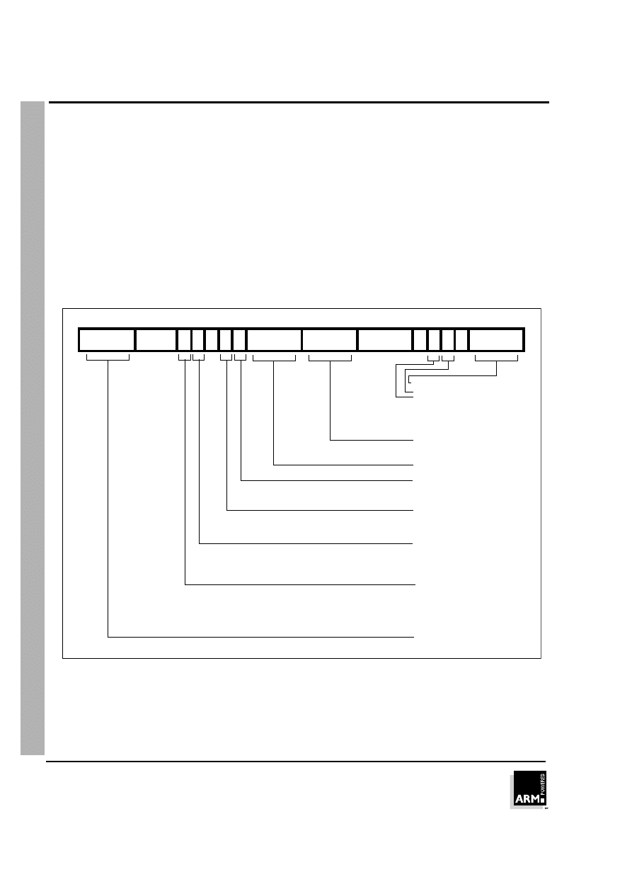
Figure 4-14: Single data transfer instructions
Cond
I
Rn
Rd
0
11
12
15
16
19
20
21
24
25
26
27
28
31
01
P U B W L
Offset
22
23
0
11
Source/Destination register
Base register
Load/Store bit
0 = Store to memory
1 = Load from memory
Write-back bit
Byte/Word bit
0 = no write-back
1 = write address into base
0 = transfer word quantity
1 = transfer byte quantity
Up/Down bit
Pre/Post indexing bit
0 = offset is an immediate value
Immediate offset
Immediate offset
Unsigned 12 bit immediate offset
1 = offset is a register
11
0
shift applied to Rm
3
4
Condition field
0 = down; subtract offset from base
1 = up; add offset to base
0 = post; add offset after transfer
1 = pre; add offset before transfer
Offset register
Shift
Rm

ARM Instruction Set - LDR, STR
ARM7TDMI Data Sheet
ARM DDI 0029E
4-29
Open Access
4.9.1 Offsets and auto-indexing
The offset from the base may be either a 12 bit unsigned binary immediate value in
the instruction, or a second register (possibly shifted in some way). The offset may be
added to (U=1) or subtracted from (U=0) the base register Rn. The offset modification
may be performed either before (pre-indexed, P=1) or after (post-indexed, P=0) the
base is used as the transfer address.
The W bit gives optional auto increment and decrement addressing modes. The
modified base value may be written back into the base (W=1), or the old base value
may be kept (W=0). In the case of post-indexed addressing, the write back bit is
redundant and is always set to zero, since the old base value can be retained by
setting the offset to zero. Therefore post-indexed data transfers always write back the
modified base. The only use of the W bit in a post-indexed data transfer is in privileged
mode code, where setting the W bit forces non-privileged mode for the transfer,
allowing the operating system to generate a user address in a system where the
memory management hardware makes suitable use of this hardware.
4.9.2 Shifted register offset
The 8 shift control bits are described in the data processing instructions section.
However, the register specified shift amounts are not available in this instruction class.
See
➲
4.5.2 Shifts on page 4-12.
4.9.3 Bytes and words
This instruction class may be used to transfer a byte (B=1) or a word (B=0) between
an ARM7TDMI register and memory.
The action of LDR(B) and STR(B) instructions is influenced by the BIGEND control
signal. The two possible configurations are described below.
Little endian configuration
A byte load (LDRB) expects the data on data bus inputs 7 through 0 if the supplied
address is on a word boundary, on data bus inputs 15 through 8 if it is a word address
plus one byte, and so on. The selected byte is placed in the bottom 8 bits of the
destination register, and the remaining bits of the register are filled with zeros. Please
see
➲
Figure 3-2: Little endian addresses of bytes within words on page 3-3.
A byte store (STRB) repeats the bottom 8 bits of the source register four times across
data bus outputs 31 through 0. The external memory system should activate the
appropriate byte subsystem to store the data.
A word load (LDR) will normally use a word aligned address. However, an address
offset from a word boundary will cause the data to be rotated into the register so that
the addressed byte occupies bits 0 to 7. This means that half-words accessed at
offsets 0 and 2 from the word boundary will be correctly loaded into bits 0 through 15
of the register. Two shift operations are then required to clear or to sign extend the
upper 16 bits. This is illustrated in
➲
Figure 4-15: Little endian offset addressing on
page 4-30.
ARM Instruction Set - LDR, STR
ARM7TDMI Data Sheet
ARM DDI 0029E
4-30
Open Access
Figure 4-15: Little endian offset addressing
A word store (STR) should generate a word aligned address. The word presented to
the data bus is not affected if the address is not word aligned. That is, bit 31 of the
register being stored always appears on data bus output 31.
Big endian configuration
A byte load (LDRB) expects the data on data bus inputs 31 through 24 if the supplied
address is on a word boundary, on data bus inputs 23 through 16 if it is a word address
plus one byte, and so on. The selected byte is placed in the bottom 8 bits of the
destination register and the remaining bits of the register are filled with zeros. Please
see
➲
Figure 3-1: Big endian addresses of bytes within words on page 3-3.
A byte store (STRB) repeats the bottom 8 bits of the source register four times across
data bus outputs 31 through 0. The external memory system should activate the
appropriate byte subsystem to store the data.
A word load (LDR) should generate a word aligned address. An address offset of 0 or
2 from a word boundary will cause the data to be rotated into the register so that the
addressed byte occupies bits 31 through 24. This means that half-words accessed at
these offsets will be correctly loaded into bits 16 through 31 of the register. A shift
operation is then required to move (and optionally sign extend) the data into the
bottom 16 bits. An address offset of 1 or 3 from a word boundary will cause the data
to be rotated into the register so that the addressed byte occupies bits 15 through 8.
A
B
C
D
memory
A+3
A+2
A+1
A
24
16
8
0
A
B
C
D
register
24
16
8
0
LDR from word aligned address
A
B
C
D
A+3
A+2
A+1
A
24
16
8
0
A
B
C
D
24
16
8
0
LDR from address offset by 2

ARM Instruction Set - LDR, STR
ARM7TDMI Data Sheet
ARM DDI 0029E
4-31
Open Access
A word store (STR) should generate a word aligned address. The word presented to
the data bus is not affected if the address is not word aligned. That is, bit 31 of the
register being stored always appears on data bus output 31.
4.9.4 Use of R15
Write-back must not be specified if R15 is specified as the base register (Rn). When
using R15 as the base register you must remember it contains an address 8 bytes on
from the address of the current instruction.
R15 must not be specified as the register offset (Rm).
When R15 is the source register (Rd) of a register store (STR) instruction, the stored
value will be address of the instruction plus 12.
4.9.5 Restriction on the use of base register
When configured for late aborts, the following example code is difficult to unwind as
the base register, Rn, gets updated before the abort handler starts. Sometimes it may
be impossible to calculate the initial value.
After an abort, the following example code is difficult to unwind as the base register,
Rn, gets updated before the abort handler starts. Sometimes it may be impossible to
calculate the initial value.
Example:
LDR
R0,[R1],R1
Therefore a post-indexed LDR or STR where Rm is the same register as Rn should
not be used.
4.9.6 Data aborts
A transfer to or from a legal address may cause problems for a memory management
system. For instance, in a system which uses virtual memory the required data may
be absent from main memory. The memory manager can signal a problem by taking
the processor ABORT input HIGH whereupon the Data Abort trap will be taken. It is
up to the system software to resolve the cause of the problem, then the instruction can
be restarted and the original program continued.
4.9.7 Instruction cycle times
Normal LDR instructions take 1S + 1N + 1I and LDR PC take 2S + 2N +1I incremental
cycles, where S,N and I are as defined in
➲
6.2 Cycle Types on page 6-2.
STR instructions take 2N incremental cycles to execute.

ARM Instruction Set - LDR, STR
ARM7TDMI Data Sheet
ARM DDI 0029E
4-32
Open Access
4.9.8 Assembler syntax
<LDR|STR>{cond}{B}{T} Rd,<Address>
where:
LDR
load from memory into a register
STR
store from a register into memory
{cond}
two-character condition mnemonic. See
➲
Table 4-2: Condition code
summary on page 4-5.
{B}
if B is present then byte transfer, otherwise word transfer
{T}
if T is present the W bit will be set in a post-indexed instruction, forcing
non-privileged mode for the transfer cycle. T is not allowed when a
pre-indexed addressing mode is specified or implied.
Rd
is an expression evaluating to a valid register number.
Rn and Rm are expressions evaluating to a register number. If Rn is R15 then the
assembler will subtract 8 from the offset value to allow for ARM7TDMI
pipelining. In this case base write-back should not be specified.
<Address> can be:
1
An expression which generates an address:
<expression>
The assembler will attempt to generate an instruction using
the PC as a base and a corrected immediate offset to address
the location given by evaluating the expression. This will be a
PC relative, pre-indexed address. If the address is out of
range, an error will be generated.
2
A pre-indexed addressing specification:
[Rn]
offset of zero
[Rn,<#expression>]{!}
offset of <expression>
bytes
[Rn,{+/-}Rm{,<shift>}]{!}
offset of +/- contents of
index register, shifted
by <shift>
3
A post-indexed addressing specification:
[Rn],<#expression>
offset of <expression>
bytes
[Rn],{+/-}Rm{,<shift>}
offset of +/- contents of
index register, shifted
as by <shift>.

ARM Instruction Set - LDR, STR
ARM7TDMI Data Sheet
ARM DDI 0029E
4-33
Open Access
<shift> general shift operation (see data processing instructions) but
you cannot specify the shift amount by a register.
{!}
writes back the base register (set the W bit) if! is present.
4.9.9 Examples
STR
R1,[R2,R4]!
; Store R1 at R2+R4 (both of which are
; registers) and write back address to
; R2.
STR
R1,[R2],R4
; Store R1 at R2 and write back
; R2+R4 to R2.
LDR
R1,[R2,#16]
; Load R1 from contents of R2+16, but
; don't write back.
LDR
R1,[R2,R3,LSL#2]
; Load R1 from contents of R2+R3*4.
LDREQBR1,[R6,#5]
; Conditionally load byte at R6+5 into
; R1 bits 0 to 7, filling bits 8 to 31
; with zeros.
STR
R1,PLACE
; Generate PC relative offset to
; address PLACE.
•
PLACE
ARM Instruction Set - LDR, STR
ARM7TDMI Data Sheet
ARM DDI 0029E
4-34
Open Access
4.10 Halfword and Signed Data Transfer
(LDRH/STRH/LDRSB/LDRSH)
The instruction is only executed if the condition is true. The various conditions are
defined in
➲
Table 4-2: Condition code summary on page 4-5. The instruction encoding
is shown in
➲
Figure 4-16: Halfword and signed data transfer with register offset,
below, and
➲
Figure 4-17: Halfword and signed data transfer with immediate offset on
page 4-35.
These instructions are used to load or store half-words of data and also load
sign-extended bytes or half-words of data. The memory address used in the transfer
is calculated by adding an offset to or subtracting an offset from a base register. The
result of this calculation may be written back into the base register if auto-indexing is
required.
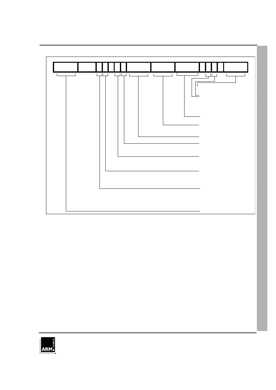
Figure 4-16: Halfword and signed data transfer with register offset
Cond
0 0 0 P U 0 W L
Rn
Rd
0
0 0
0
Rm
0
3
4
7
8
11
12
15
16
19
20
21
22
27
28
31
Offset register
Base register
S H
Source/Destination
00 = SWP instruction
01 = Unsigned halfwords
0 = store to memory
1 = load from memory
Load/Store
1 S H 1
10 = Signed byte
11 = Signed halfwords
register
0 = no write-back
1 = write address into base
Write-back
0 = down: subtract offset from
base
Up/Down
1 = up: add offset to base
0 = post: add/subtract offset
Pre/Post indexing
after transfer
1 = pre: add/subtract offset
before transfer
Condition field
23
24
25
5
6
ARM Instruction Set - LDR, STR
ARM7TDMI Data Sheet
ARM DDI 0029E
4-35
Open Access
Figure 4-17: Halfword and signed data transfer with immediate offset
4.10.1 Offsets and auto-indexing
The offset from the base may be either a 8-bit unsigned binary immediate value in the
instruction, or a second register. The 8-bit offset is formed by concatenating bits 11 to
8 and bits 3 to 0 of the instruction word, such that bit 11 becomes the MSB and bit 0
becomes the LSB. The offset may be added to (U=1) or subtracted from (U=0) the
base register Rn. The offset modification may be performed either before (pre-
indexed, P=1) or after (post-indexed, P=0) the base register is used as the transfer
address.
The W bit gives optional auto-increment and decrement addressing modes. The
modified base value may be written back into the base (W=1), or the old base may be
kept (W=0). In the case of post-indexed addressing, the write back bit is redundant and
is always set to zero, since the old base value can be retained if necessary by setting
the offset to zero. Therefore post-indexed data transfers always write back the
modified base.
The Write-back bit should not be set high (W=1) when post-indexed addressing is
selected.
Cond
0 0 0 P U 1 W L
Rn
Rd
Offset
0
3
4
7
8
11
12
15
16
19
20
21
22
27
28
31
Immediate Offset
Base register
S H
Source/Destination
00 = SWP instruction
01 = Unsigned halfwords
0 = store to memory
1 = load from memory
Load/Store
1 S H 1
10 = Signed byte
11 = Signed halfwords
register
0 = no write-back
1 = write address into base
Write-back
0 = down: subtract offset from
base
Up/Down
1 = up: add offset to base
0 = post: add/subtract offset
Pre/Post indexing
after transfer
1 = pre: add/subtract offset
before transfer
Condition field
23
24
25
5
6
Offset
Immediate Offset
(High nibble)
(Low nibble)

ARM Instruction Set - LDR, STR
ARM7TDMI Data Sheet
ARM DDI 0029E
4-36
Open Access
4.10.2 Halfword load and stores
Setting S=0 and H=1 may be used to transfer unsigned Half-words between an
ARM7TDMI register and memory.
The action of LDRH and STRH instructions is influenced by the BIGEND control
signal. The two possible configurations are described in the section below.
4.10.3 Signed byte and halfword loads
The S bit controls the loading of sign-extended data. When S=1 the H bit selects
between Bytes (H=0) and Half-words (H=1). The L bit should not be set low (Store)
when Signed (S=1) operations have been selected.
The LDRSB instruction loads the selected Byte into bits 7 to 0 of the destination
register and bits 31 to 8 of the destination register are set to the value of bit 7, the sign
bit.
The LDRSH instruction loads the selected Half-word into bits 15 to 0 of the destination
register and bits 31 to 16 of the destination register are set to the value of bit 15, the
sign bit.
The action of the LDRSB and LDRSH instructions is influenced by the BIGEND control
signal. The two possible configurations are described in the following section.
4.10.4 Endianness and byte/halfword selection
Little endian configuration
A signed byte load (LDRSB) expects data on data bus inputs 7 through to 0 if the
supplied address is on a word boundary, on data bus inputs 15 through to 8 if it is a
word address plus one byte, and so on. The selected byte is placed in the bottom 8 bit
of the destination register, and the remaining bits of the register are filled with the sign
bit, bit 7 of the byte. Please see
➲
Figure 3-2: Little endian addresses of bytes within
words on page 3-3
A halfword load (LDRSH or LDRH) expects data on data bus inputs 15 through to 0 if
the supplied address is on a word boundary and on data bus inputs 31 through to 16
if it is a halfword boundary, (A[1]=1).The supplied address should always be on a
halfword boundary. If bit 0 of the supplied address is HIGH then the ARM7TDMI will
load an unpredictable value. The selected halfword is placed in the bottom 16 bits of
the destination register. For unsigned half-words (LDRH), the top 16 bits of the register
are filled with zeros and for signed half-words (LDRSH) the top 16 bits are filled with
the sign bit, bit 15 of the halfword.
A halfword store (STRH) repeats the bottom 16 bits of the source register twice across
the data bus outputs 31 through to 0. The external memory system should activate the
appropriate halfword subsystem to store the data. Note that the address must be
halfword aligned, if bit 0 of the address is HIGH this will cause unpredictable
behaviour.

ARM Instruction Set - LDR, STR
ARM7TDMI Data Sheet
ARM DDI 0029E
4-37
Open Access
Big endian configuration
A signed byte load (LDRSB) expects data on data bus inputs 31 through to 24 if the
supplied address is on a word boundary, on data bus inputs 23 through to 16 if it is a
word address plus one byte, and so on. The selected byte is placed in the bottom 8 bit
of the destination register, and the remaining bits of the register are filled with the sign
bit, bit 7 of the byte. Please see
➲
Figure 3-1: Big endian addresses of bytes within
words on page 3-3
A halfword load (LDRSH or LDRH) expects data on data bus inputs 31 through to 16
if the supplied address is on a word boundary and on data bus inputs 15 through to 0
if it is a halfword boundary, (A[1]=1). The supplied address should always be on a
halfword boundary. If bit 0 of the supplied address is HIGH then the ARM7TDMI will
load an unpredictable value. The selected halfword is placed in the bottom 16 bits of
the destination register. For unsigned half-words (LDRH), the top 16 bits of the register
are filled with zeros and for signed half-words (LDRSH) the top 16 bits are filled with
the sign bit, bit 15 of the halfword.
A halfword store (STRH) repeats the bottom 16 bits of the source register twice across
the data bus outputs 31 through to 0. The external memory system should activate the
appropriate halfword subsystem to store the data. Note that the address must be
halfword aligned, if bit 0 of the address is HIGH this will cause unpredictable
behaviour.
4.10.5 Use of R15
Write-back should not be specified if R15 is specified as the base register (Rn). When
using R15 as the base register you must remember it contains an address 8 bytes on
from the address of the current instruction.
R15 should not be specified as the register offset (Rm).
When R15 is the source register (Rd) of a Half-word store (STRH) instruction, the
stored address will be address of the instruction plus 12.
4.10.6 Data aborts
A transfer to or from a legal address may cause problems for a memory management
system. For instance, in a system which uses virtual memory the required data may
be absent from the main memory. The memory manager can signal a problem by
taking the processor ABORT input HIGH whereupon the Data Abort trap will be taken.
It is up to the system software to resolve the cause of the problem, then the instruction
can be restarted and the original program continued.
4.10.7 Instruction cycle times
Normal LDR(H,SH,SB) instructions take 1S + 1N + 1I
LDR(H,SH,SB) PC take 2S + 2N + 1I incremental cycles.
S,N and I are defined in
➲
6.2 Cycle Types on page 6-2
.
STRH instructions take 2N incremental cycles to execute.

ARM Instruction Set - LDR, STR
ARM7TDMI Data Sheet
ARM DDI 0029E
4-38
Open Access
4.10.8 Assembler syntax
<LDR|STR>{cond}<H|SH|SB> Rd,<address>
LDR
load from memory into a register
STR
Store from a register into memory
{cond}
two-character condition mnemonic. See
➲
Table 4-2: Condition code
summary on page 4-5.
H
Transfer halfword quantity
SB
Load sign extended byte (Only valid for LDR)
SH
Load sign extended halfword (Only valid for LDR)
Rd
is an expression evaluating to a valid register number.
<address> can be:
1
An expression which generates an address:
<expression>
The assembler will attempt to generate an instruction using
the PC as a base and a corrected immediate offset to address
the location given by evaluating the expression. This will be a
PC relative, pre-indexed address. If the address is out of
range, an error will be generated.
2
A pre-indexed addressing specification:
[Rn]
offset of zero
[Rn,<#expression>]{!}
offset of <expression> bytes
[Rn,{+/-}Rm]{!}
offset of +/- contents of
index register
3
A post-indexed addressing specification:
[Rn],<#expression>
offset of <expression> bytes
[Rn],{+/-}Rm
offset of +/- contents of
index register.
Rn and Rm are expressions evaluating to a register number.
If Rn is R15 then the assembler will subtract 8 from the offset
value to allow for ARM7TDMI pipelining. In this case base
write-back should not be specified.
{!}
writes back the base register (set the W bit) if ! is present.

ARM Instruction Set - LDR, STR
ARM7TDMI Data Sheet
ARM DDI 0029E
4-39
Open Access
4.10.9 Examples
LDRH
R1,[R2,-R3]!
; Load R1 from the contents of the
; halfword address contained in
; R2-R3 (both of which are registers)
; and write back address to R2
STRH
R3,[R4,#14]
; Store the halfword in R3 at R14+14
; but don't write back.
LDRSB
R8,[R2],#-223
; Load R8 with the sign extended
; contents of the byte address
; contained in R2 and write back
; R2-223 to R2.
LDRNESH
R11,[R0]
; conditionally load R11 with the sign
; extended contents of the halfword
; address contained in R0.
HERE
; Generate PC relative offset to
; address FRED.
; Store the halfword in R5 at address
; FRED.
STRH
R5, [PC, #(FRED-HERE-8)]
.
FRED
ARM Instruction Set - LDM, STM
ARM7TDMI Data Sheet
ARM DDI 0029E
4-40
Open Access
4.11 Block Data Transfer (LDM, STM)
The instruction is only executed if the condition is true. The various conditions are
defined in
➲
Table 4-2: Condition code summary on page 4-5. The instruction encoding
is shown in
➲
Figure 4-18: Block data transfer instructions.
Block data transfer instructions are used to load (LDM) or store (STM) any subset of
the currently visible registers. They support all possible stacking modes, maintaining
full or empty stacks which can grow up or down memory, and are very efficient
instructions for saving or restoring context, or for moving large blocks of data around
main memory.
4.11.1 The register list
The instruction can cause the transfer of any registers in the current bank (and
non-user mode programs can also transfer to and from the user bank, see below). The
register list is a 16 bit field in the instruction, with each bit corresponding to a register.
A 1 in bit 0 of the register field will cause R0 to be transferred, a 0 will cause it not to
be transferred; similarly bit 1 controls the transfer of R1, and so on.
Any subset of the registers, or all the registers, may be specified. The only restriction
is that the register list should not be empty.
Whenever R15 is stored to memory the stored value is the address of the STM
instruction plus 12.
Figure 4-18: Block data transfer instructions
Cond
Rn
0
15
16
19
20
21
24
25
27
28
31
P U
W L
22
23
100
S
Register list
Base register
Load/Store bit
0 = Store to memory
1 = Load from memory
Write-back bit
0 = no write-back
1 = write address into base
Up/Down bit
Pre/Post indexing bit
0 = down; subtract offset from base
1 = up; add offset to base
0 = post; add offset after transfer
1 = pre; add offset before transfer
PSR & force user bit
0 = do not load PSR or force user mode
1 = load PSR or force user mode
Condition field
ARM Instruction Set - LDM, STM
ARM7TDMI Data Sheet
ARM DDI 0029E
4-41
Open Access
4.11.2 Addressing modes
The transfer addresses are determined by the contents of the base register (Rn), the
pre/post bit (P) and the up/down bit (U). The registers are transferred in the order
lowest to highest, so R15 (if in the list) will always be transferred last. The lowest
register also gets transferred to/from the lowest memory address. By way of
illustration, consider the transfer of R1, R5 and R7 in the case where Rn=0x1000 and
write back of the modified base is required (W=1).
➲
Figure 4-19: Post-increment
addressing,
➲
Figure 4-20: Pre-increment addressing,
➲
Figure 4-21: Post-decrement
addressing and
➲
Figure 4-22: Pre-decrement addressing show the sequence of
register transfers, the addresses used, and the value of Rn after the instruction has
completed.
In all cases, had write back of the modified base not been required (W=0), Rn would
have retained its initial value of 0x1000 unless it was also in the transfer list of a load
multiple register instruction, when it would have been overwritten with the loaded
value.
4.11.3 Address alignment
The address should normally be a word aligned quantity and non-word aligned
addresses do not affect the instruction. However, the bottom 2 bits of the address will
appear on A[1:0] and might be interpreted by the memory system.
Figure 4-19: Post-increment addressing
0x100C
0x1000
0x0FF4
Rn
1
0x100C
0x1000
0x0FF4
2
R1
0x100C
0x1000
0x0FF4
3
0x100C
0x1000
0x0FF4
4
R1
R7
R5
R1
R5
Rn
ARM Instruction Set - LDM, STM
ARM7TDMI Data Sheet
ARM DDI 0029E
4-42
Open Access
Figure 4-20: Pre-increment addressing
Figure 4-21: Post-decrement addressing
0x100C
0x1000
0x0FF4
Rn
1
0x100C
0x1000
0x0FF4
2
R1
0x100C
0x1000
0x0FF4
3
0x100C
0x1000
0x0FF4
4
R1
R7
R5
R1
R5
Rn
0x100C
0x1000
0x0FF4
Rn
1
0x100C
0x1000
0x0FF4
2
R1
0x100C
0x1000
0x0FF4
3
0x100C
0x1000
0x0FF4
4
R1
R7
R5
R1
R5
Rn
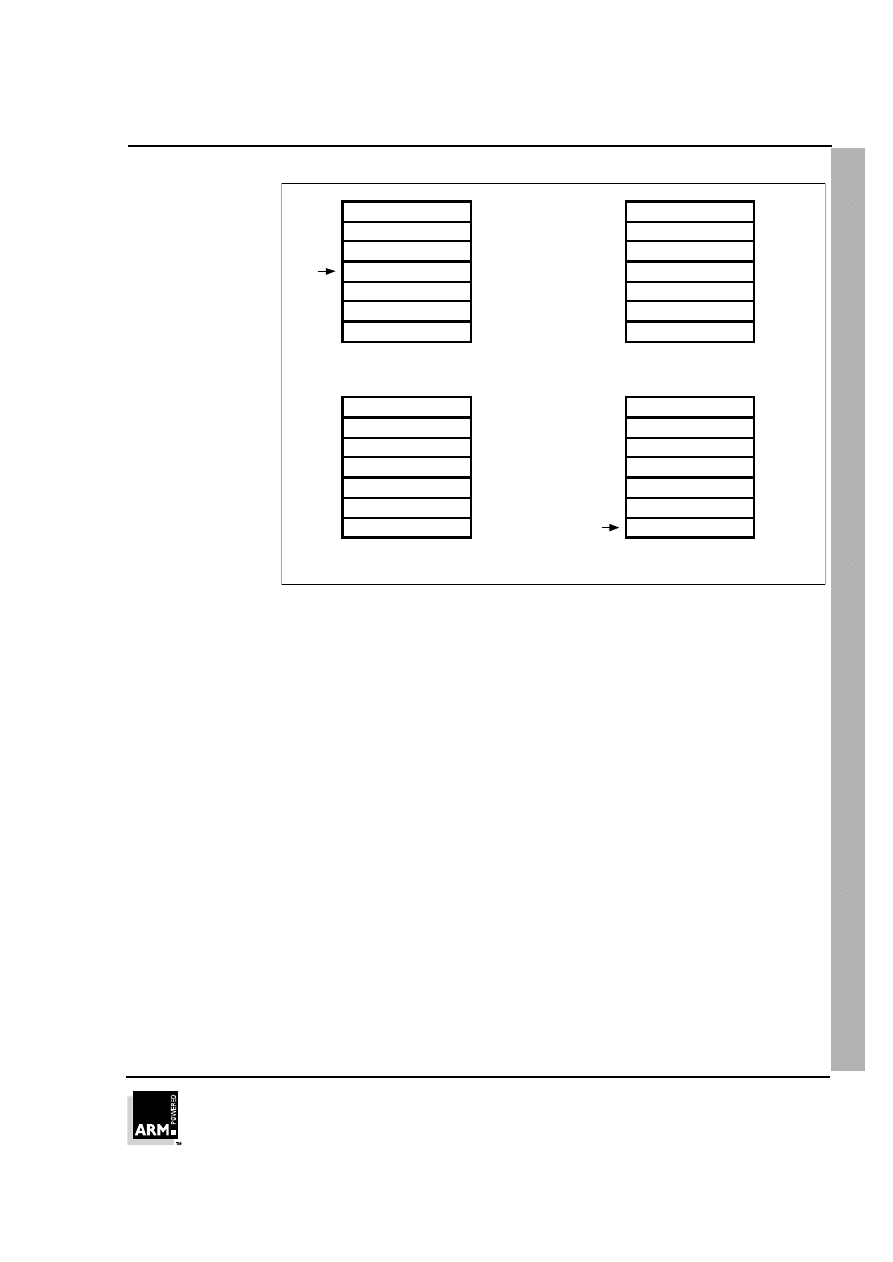
ARM Instruction Set - LDM, STM
ARM7TDMI Data Sheet
ARM DDI 0029E
4-43
Open Access
Figure 4-22: Pre-decrement addressing
4.11.4 Use of the S bit
When the S bit is set in a LDM/STM instruction its meaning depends on whether or not
R15 is in the transfer list and on the type of instruction. The S bit should only be set if
the instruction is to execute in a privileged mode.
LDM with R15 in transfer list and S bit set (Mode changes)
If the instruction is a LDM then SPSR_<mode> is transferred to CPSR at the same
time as R15 is loaded.
STM with R15 in transfer list and S bit set (User bank transfer)
The registers transferred are taken from the User bank rather than the bank
corresponding to the current mode. This is useful for saving the user state on process
switches. Base write-back should not be used when this mechanism is employed.
R15 not in list and S bit set (User bank transfer)
For both LDM and STM instructions, the User bank registers are transferred rather
than the register bank corresponding to the current mode. This is useful for saving the
user state on process switches. Base write-back should not be used when this
mechanism is employed.
When the instruction is LDM, care must be taken not to read from a banked register
during the following cycle (inserting a dummy instruction such as MOV R0, R0 after
the LDM will ensure safety).
0x100C
0x1000
0x0FF4
Rn
1
0x100C
0x1000
0x0FF4
2
R1
0x100C
0x1000
0x0FF4
3
0x100C
0x1000
0x0FF4
4
R1
R7
R5
R1
R5
Rn

ARM Instruction Set - LDM, STM
ARM7TDMI Data Sheet
ARM DDI 0029E
4-44
Open Access
4.11.5 Use of R15 as the base
R15 should not be used as the base register in any LDM or STM instruction.
4.11.6 Inclusion of the base in the register list
When write-back is specified, the base is written back at the end of the second cycle
of the instruction. During a STM, the first register is written out at the start of the
second cycle. A STM which includes storing the base, with the base as the first register
to be stored, will therefore store the unchanged value, whereas with the base second
or later in the transfer order, will store the modified value. A LDM will always overwrite
the updated base if the base is in the list.
4.11.7 Data aborts
Some legal addresses may be unacceptable to a memory management system, and
the memory manager can indicate a problem with an address by taking the ABORT
signal HIGH. This can happen on any transfer during a multiple register load or store,
and must be recoverable if ARM7TDMI is to be used in a virtual memory system.
Aborts during STM instructions
If the abort occurs during a store multiple instruction, ARM7TDMI takes little action
until the instruction completes, whereupon it enters the data abort trap. The memory
manager is responsible for preventing erroneous writes to the memory. The only
change to the internal state of the processor will be the modification of the base
register if write-back was specified, and this must be reversed by software (and the
cause of the abort resolved) before the instruction may be retried.
Aborts during LDM instructions
When ARM7TDMI detects a data abort during a load multiple instruction, it modifies
the operation of the instruction to ensure that recovery is possible.
1
Overwriting of registers stops when the abort happens. The aborting load will
not take place but earlier ones may have overwritten registers. The PC is
always the last register to be written and so will always be preserved.
2
The base register is restored, to its modified value if write-back was
requested. This ensures recoverability in the case where the base register is
also in the transfer list, and may have been overwritten before the abort
occurred.
The data abort trap is taken when the load multiple has completed, and the system
software must undo any base modification (and resolve the cause of the abort) before
restarting the instruction.
4.11.8 Instruction cycle times
Normal LDM instructions take nS + 1N + 1I and LDM PC takes (n+1)S + 2N + 1I
incremental cycles, where S,N and I are as defined in
➲
6.2 Cycle Types on page 6-2.
STM instructions take (n-1)S + 2N incremental cycles to execute, where
n is the
number of words transferred.
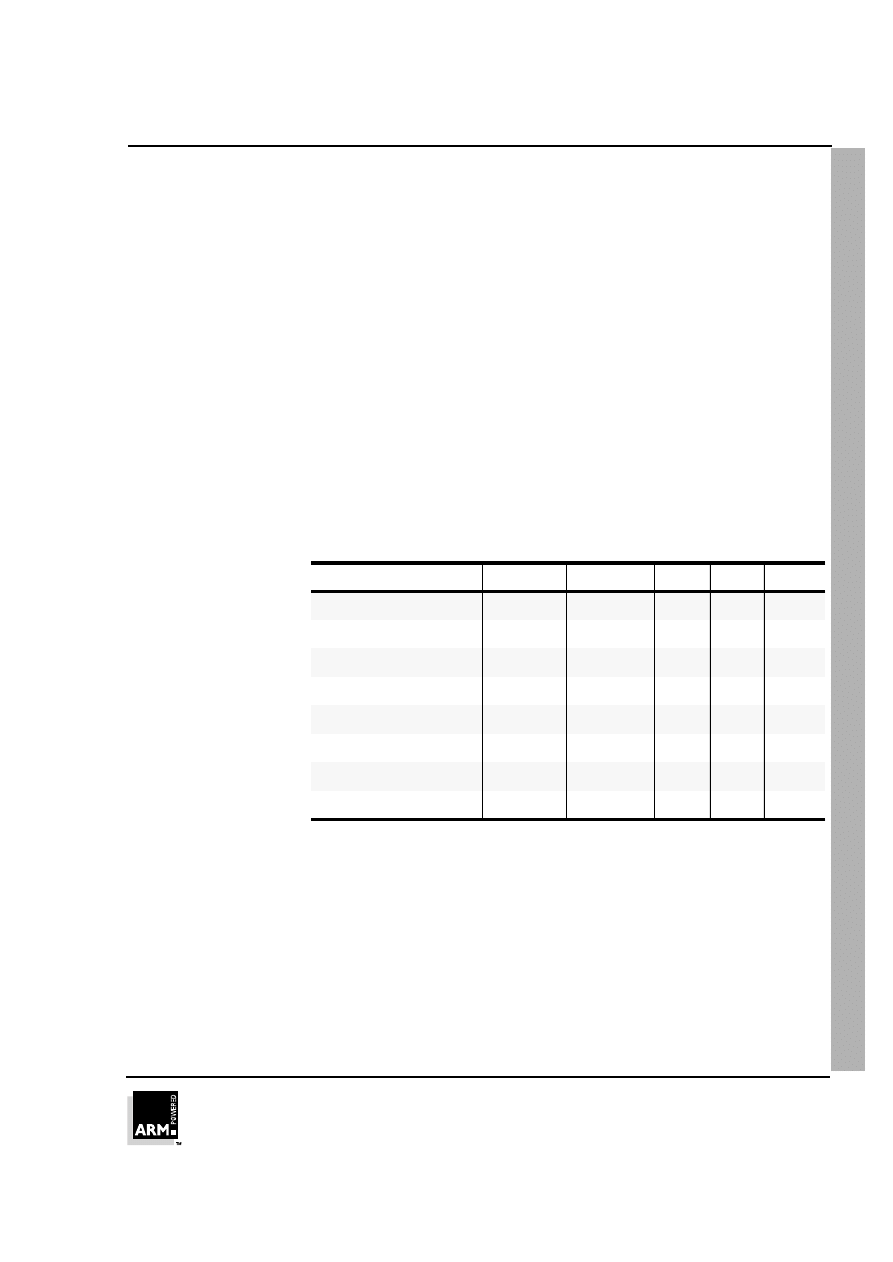
ARM Instruction Set - LDM, STM
ARM7TDMI Data Sheet
ARM DDI 0029E
4-45
Open Access
4.11.9 Assembler syntax
<LDM|STM>{cond}<FD|ED|FA|EA|IA|IB|DA|DB> Rn{!},<Rlist>{^}
where:
{cond}
two character condition mnemonic. See
➲
Table 4-2: Condition code
summary on page 4-5.
Rn
is an expression evaluating to a valid register number
<Rlist>
is a list of registers and register ranges enclosed in {} (e.g. {R0,R2-
R7,R10}).
{!}
if present requests write-back (W=1), otherwise W=0
{^}
if present set S bit to load the CPSR along with the PC, or force
transfer of user bank when in privileged mode
Addressing mode names
There are different assembler mnemonics for each of the addressing modes,
depending on whether the instruction is being used to support stacks or for other
purposes. The equivalence between the names and the values of the bits in the
instruction are shown in the following table:
FD, ED, FA, EA define pre/post indexing and the up/down bit by reference to the form
of stack required. The F and E refer to a “full” or “empty” stack, i.e. whether a pre-index
has to be done (full) before storing to the stack. The A and D refer to whether the stack
is ascending or descending. If ascending, a STM will go up and LDM down, if
descending, vice-versa.
IA, IB, DA, DB allow control when LDM/STM are not being used for stacks and simply
mean Increment After, Increment Before, Decrement After, Decrement Before.
Name
Stack
Other
L bit
P bit
U bit
pre-increment load
LDMED
LDMIB
1
1
1
post-increment load
LDMFD
LDMIA
1
0
1
pre-decrement load
LDMEA
LDMDB
1
1
0
post-decrement load
LDMFA
LDMDA
1
0
0
pre-increment store
STMFA
STMIB
0
1
1
post-increment store
STMEA
STMIA
0
0
1
pre-decrement store
STMFD
STMDB
0
1
0
post-decrement store
STMED
STMDA
0
0
0
Table 4-6: Addressing mode names

ARM Instruction Set - LDM, STM
ARM7TDMI Data Sheet
ARM DDI 0029E
4-46
Open Access
4.11.10Examples
LDMFD SP!,{R0,R1,R2}
; Unstack 3 registers.
STMIA R0,{R0-R15}
; Save all registers.
LDMFD SP!,{R15}
; R15 <- (SP),CPSR unchanged.
LDMFD SP!,{R15}^
; R15 <- (SP), CPSR <- SPSR_mode
; (allowed only in privileged modes).
STMFD R13,{R0-R14}^
; Save user mode regs on stack
; (allowed only in privileged modes).
These instructions may be used to save state on subroutine entry, and restore it
efficiently on return to the calling routine:
STMED SP!,{R0-R3,R14}
; Save R0 to R3 to use as workspace
; and R14 for returning.
BL
somewhere
; This nested call will overwrite R14
LDMED SP!,{R0-R3,R15}
; restore workspace and return.
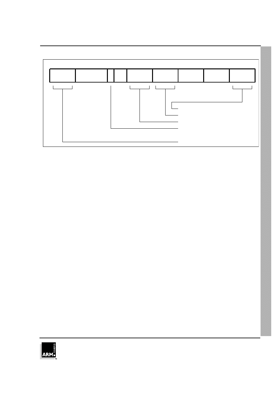
ARM Instruction Set - SWP
ARM7TDMI Data Sheet
ARM DDI 0029E
4-47
Open Access
4.12 Single Data Swap (SWP)
Figure 4-23: Swap instruction
The instruction is only executed if the condition is true. The various conditions are
defined in
➲
Table 4-2: Condition code summary on page 4-5. The instruction encoding
is shown in
➲
Figure 4-23: Swap instruction.
The data swap instruction is used to swap a byte or word quantity between a register
and external memory. This instruction is implemented as a memory read followed by
a memory write which are “locked” together (the processor cannot be interrupted until
both operations have completed, and the memory manager is warned to treat them as
inseparable). This class of instruction is particularly useful for implementing software
semaphores.
The swap address is determined by the contents of the base register (Rn). The
processor first reads the contents of the swap address. Then it writes the contents of
the source register (Rm) to the swap address, and stores the old memory contents in
the destination register (Rd). The same register may be specified as both the source
and destination.
The LOCK output goes HIGH for the duration of the read and write operations to signal
to the external memory manager that they are locked together, and should be allowed
to complete without interruption. This is important in multi-processor systems where
the swap instruction is the only indivisible instruction which may be used to implement
semaphores; control of the memory must not be removed from a processor while it is
performing a locked operation.
4.12.1 Bytes and words
This instruction class may be used to swap a byte (B=1) or a word (B=0) between an
ARM7TDMI register and memory. The SWP instruction is implemented as a LDR
followed by a STR and the action of these is as described in the section on single data
transfers. In particular, the description of Big and Little Endian configuration applies to
the SWP instruction.
0
11
12
15
16
19
20
27
28
31
23
7
8
4
3
Condition field
Cond
Rn
Rd
1001
0000
Rm
00
B
00010
22 21
Destination register
Source register
Base register
Byte/Word bit
0 = swap word quantity
1 = swap byte quantity

ARM Instruction Set - SWP
ARM7TDMI Data Sheet
ARM DDI 0029E
4-48
Open Access
4.12.2 Use of R15
Do not use R15 as an operand (Rd, Rn or Rs) in a SWP instruction.
4.12.3 Data aborts
If the address used for the swap is unacceptable to a memory management system,
the memory manager can flag the problem by driving ABORT HIGH. This can happen
on either the read or the write cycle (or both), and in either case, the Data Abort trap
will be taken. It is up to the system software to resolve the cause of the problem, then
the instruction can be restarted and the original program continued.
4.12.4 Instruction cycle times
Swap instructions take 1S + 2N +1I incremental cycles to execute, where S,N and I
are as defined in
➲
6.2 Cycle Types on page 6-2.
4.12.5 Assembler syntax
<SWP>{cond}{B} Rd,Rm,[Rn]
{cond}
two-character condition mnemonic. See
➲
Table 4-2:
Condition code summary on page 4-5.
{B}
if B is present then byte transfer, otherwise word transfer
Rd,Rm,Rn
are expressions evaluating to valid register numbers
4.12.6 Examples
SWP
R0,R1,[R2]
; Load R0 with the word addressed by R2, and
; store R1 at R2.
SWPB
R2,R3,[R4]
; Load R2 with the byte addressed by R4, and
; store bits 0 to 7 of R3 at R4.
SWPEQ R0,R0,[R1]
; Conditionally swap the contents of the
; word addressed by R1 with R0.
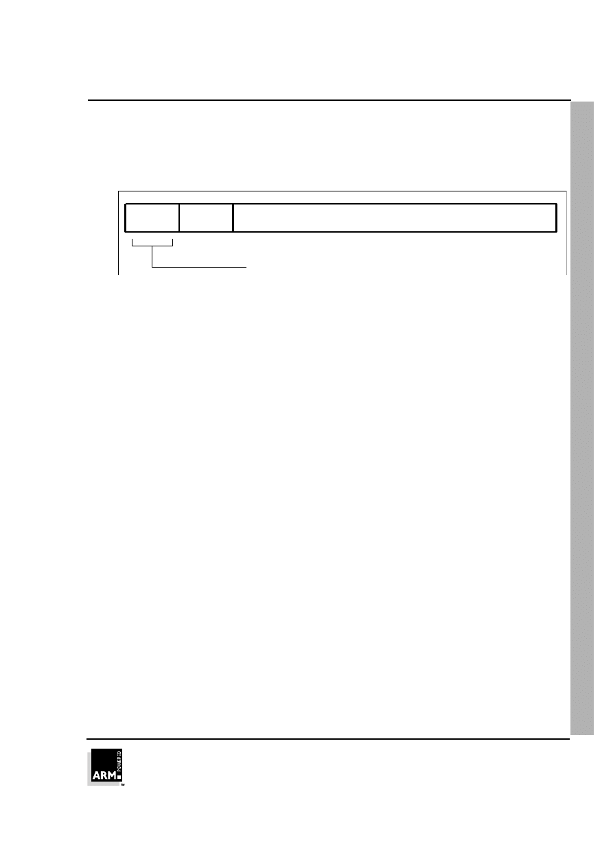
ARM Instruction Set - SWI
ARM7TDMI Data Sheet
ARM DDI 0029E
4-49
Open Access
4.13 Software Interrupt (SWI)
The instruction is only executed if the condition is true. The various conditions are
defined in
➲
Table 4-2: Condition code summary on page 4-5. The instruction encoding
is shown in
➲
Figure 4-24: Software interrupt instruction, below.
Figure 4-24: Software interrupt instruction
The software interrupt instruction is used to enter Supervisor mode in a controlled
manner. The instruction causes the software interrupt trap to be taken, which effects
the mode change. The PC is then forced to a fixed value (0x08) and the CPSR is
saved in SPSR_svc. If the SWI vector address is suitably protected (by external
memory management hardware) from modification by the user, a fully protected
operating system may be constructed.
4.13.1 Return from the supervisor
The PC is saved in R14_svc upon entering the software interrupt trap, with the PC
adjusted to point to the word after the SWI instruction. MOVS PC,R14_svc will return
to the calling program and restore the CPSR.
Note that the link mechanism is not re-entrant, so if the supervisor code wishes to use
software interrupts within itself it must first save a copy of the return address and
SPSR.
4.13.2 Comment field
The bottom 24 bits of the instruction are ignored by the processor, and may be used
to communicate information to the supervisor code. For instance, the supervisor may
look at this field and use it to index into an array of entry points for routines which
perform the various supervisor functions.
4.13.3 Instruction cycle times
Software interrupt instructions take 2S + 1N incremental cycles to execute, where S
and N are as defined in
➲
6.2 Cycle Types on page 6-2.
31
28 27
24 23
0
Condition field
1111
Cond
Comment field (ignored by Processor)

ARM Instruction Set - SWI
ARM7TDMI Data Sheet
ARM DDI 0029E
4-50
Open Access
4.13.4 Assembler syntax
SWI{cond} <expression>
{cond}
two character condition mnemonic,
➲
Table 4-2: Condition
code summary on page 4-5.
<expression>
is evaluated and placed in the comment field (which is
ignored by ARM7TDMI).
4.13.5 Examples
SWI
ReadC
; Get next character from read stream.
SWI
WriteI+”k”
; Output a “k” to the write stream.
SWINE 0
; Conditionally call supervisor
; with 0 in comment field.
Supervisor code
The previous examples assume that suitable supervisor code exists, for instance:
0x08 B Supervisor
; SWI entry point
EntryTable
; addresses of supervisor routines
DCD ZeroRtn
DCD ReadCRtn
DCD WriteIRtn
. . .
Zero
EQU 0
ReadC EQU 256
WriteI EQU 512
Supervisor
; SWI has routine required in bits 8-23 and data (if any) in
; bits 0-7.
; Assumes R13_svc points to a suitable stack
STMFD R13,{R0-R2,R14}
; Save work registers and return
; address.
LDR
R0,[R14,#-4]
; Get SWI instruction.
BIC
R0,R0,#0xFF000000 ; Clear top 8 bits.
MOV
R1,R0,LSR#8
; Get routine offset.
ADR
R2,EntryTable
; Get start address of entry table.
LDR
R15,[R2,R1,LSL#2] ; Branch to appropriate routine.
WriteIRtn
; Enter with character in R0 bits 0-7.
. . . . . .
LDMFD R13,{R0-R2,R15}^
; Restore workspace and return,
; restoring processor mode and flags.
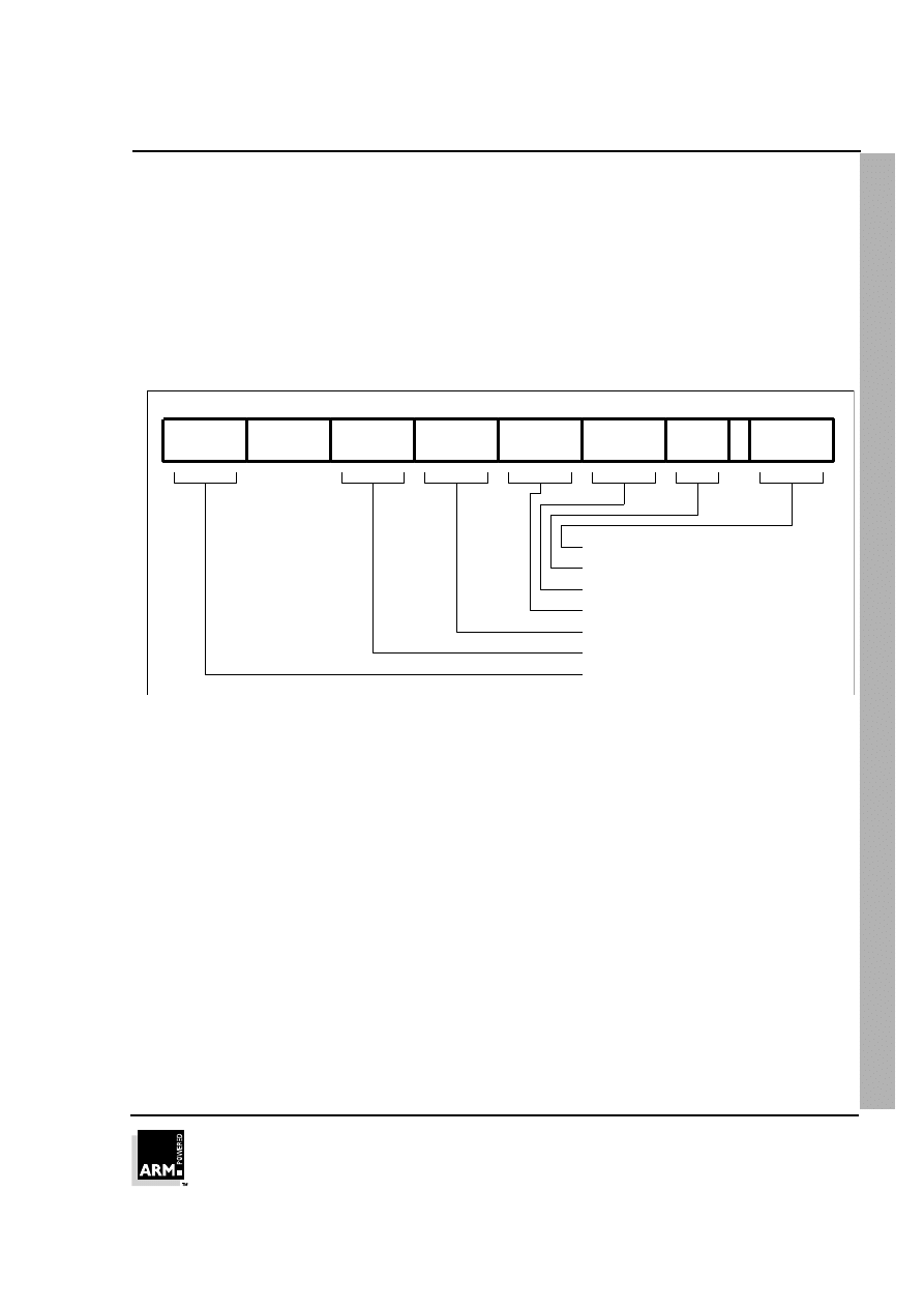
ARM Instruction Set - CDP
ARM7TDMI Data Sheet
ARM DDI 0029E
4-51
Open Access
4.14 Coprocessor Data Operations (CDP)
The instruction is only executed if the condition is true. The various conditions are
defined in
➲
Table 4-2: Condition code summary on page 4-5. The instruction encoding
is shown in
➲
Figure 4-25: Coprocessor data operation instruction.
This class of instruction is used to tell a coprocessor to perform some internal
operation. No result is communicated back to ARM7TDMI, and it will not wait for the
operation to complete. The coprocessor could contain a queue of such instructions
awaiting execution, and their execution can overlap other activity, allowing the
coprocessor and ARM7TDMI to perform independent tasks in parallel.
Figure 4-25: Coprocessor data operation instruction
4.14.1 The coprocessor fields
Only bit 4 and bits 24 to 31 are significant to ARM7TDMI. The remaining bits are used
by coprocessors. The above field names are used by convention, and particular
coprocessors may redefine the use of all fields except CP# as appropriate. The CP#
field is used to contain an identifying number (in the range 0 to 15) for each
coprocessor, and a coprocessor will ignore any instruction which does not contain its
number in the CP# field.
The conventional interpretation of the instruction is that the coprocessor should
perform an operation specified in the CP Opc field (and possibly in the CP field) on the
contents of CRn and CRm, and place the result in CRd.
4.14.2 Instruction cycle times
Coprocessor data operations take 1S + bI incremental cycles to execute, where
b is
the number of cycles spent in the coprocessor busy-wait loop.
S and I are as defined in
➲
6.2 Cycle Types on page 6-2.
Cond
0
11
12
15
16
19
20
24
27
28
31
23
CRd
CP#
7
8
1110
CP Opc
CRn
CP
0
CRm
5
4
3
Coprocessor number
Condition field
Coprocessor information
Coprocessor operand register
Coprocessor destination register
Coprocessor operand register
Coprocessor operation code

ARM Instruction Set - CDP
ARM7TDMI Data Sheet
ARM DDI 0029E
4-52
Open Access
4.14.3 Assembler syntax
CDP{cond} p#,<expression1>,cd,cn,cm{,<expression2>}
{cond}
two character condition mnemonic. See
➲
Table 4-2:
Condition code summary on page 4-5.
p#
the unique number of the required coprocessor
<expression1>
evaluated to a constant and placed in the CP Opc field
cd, cn and cm
evaluate to the valid coprocessor register numbers CRd, CRn
and CRm respectively
<expression2>
where present is evaluated to a constant and placed in the
CP field
4.14.4 Examples
CDP
p1,10,c1,c2,c3
; Request coproc 1 to do operation 10
; on CR2 and CR3, and put the result
; in CR1.
CDPEQ p2,5,c1,c2,c3,2
; If Z flag is set request coproc 2
; to do operation 5 (type 2) on CR2
; and CR3,and put the result in CR1.
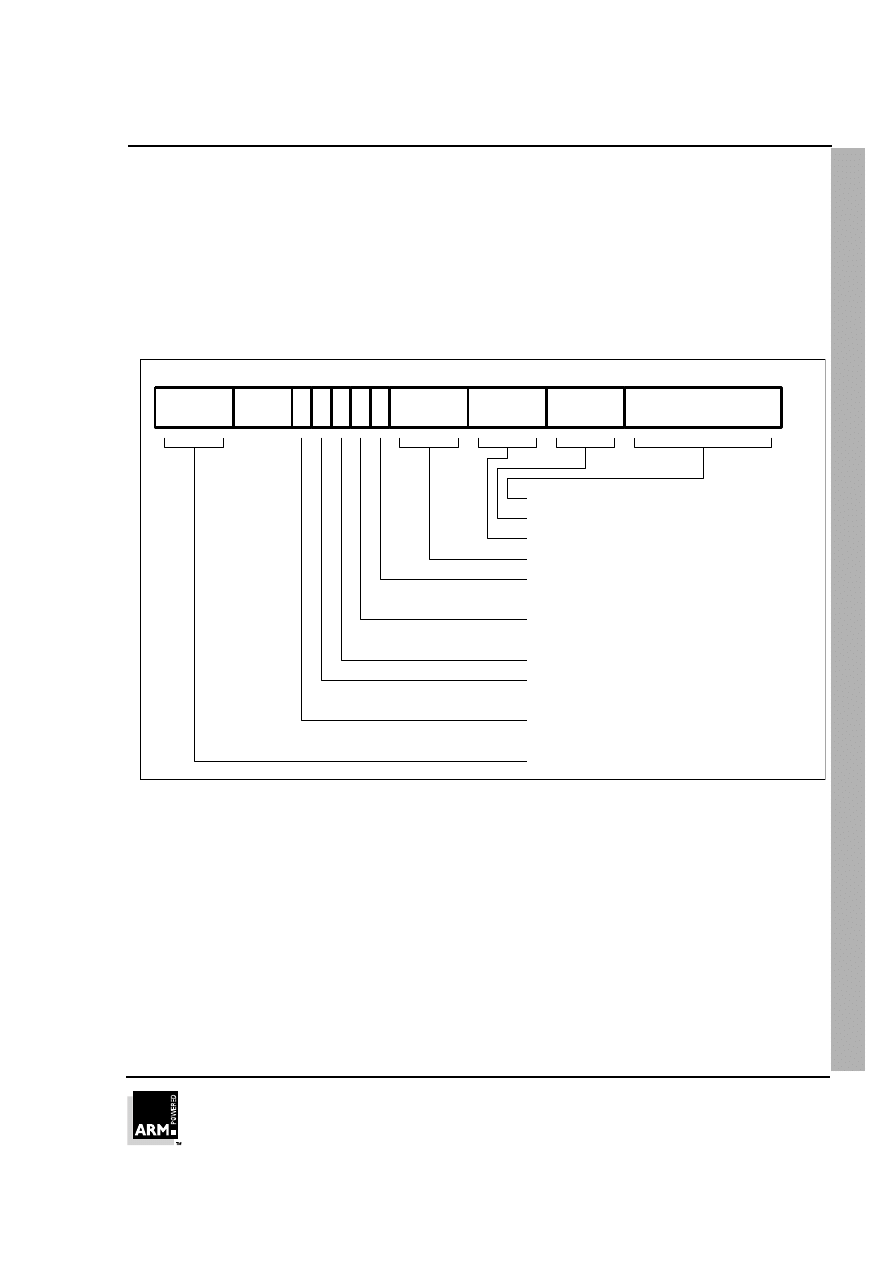
ARM Instruction Set - LDC, STC
ARM7TDMI Data Sheet
ARM DDI 0029E
4-53
Open Access
4.15 Coprocessor Data Transfers (LDC, STC)
The instruction is only executed if the condition is true. The various conditions are
defined in
➲
Table 4-2: Condition code summary on page 4-5. The instruction encoding
is shown in
➲
Figure 4-26: Coprocessor data transfer instructions.
This class of instruction is used to load (LDC) or store (STC) a subset of a
coprocessors’s registers directly to memory. ARM7TDMI is responsible for supplying
the memory address, and the coprocessor supplies or accepts the data and controls
the number of words transferred.
Figure 4-26: Coprocessor data transfer instructions
4.15.1 The coprocessor fields
The CP# field is used to identify the coprocessor which is required to supply or accept
the data, and a coprocessor will only respond if its number matches the contents of
this field.
The CRd field and the N bit contain information for the coprocessor which may be
interpreted in different ways by different coprocessors, but by convention CRd is the
register to be transferred (or the first register where more than one is to be
transferred), and the N bit is used to choose one of two transfer length options. For
instance N=0 could select the transfer of a single register, and N=1 could select the
transfer of all the registers for context switching.
Cond
Rn
0
11
12
15
16
19
20
21
24
25
27
28
31
P U
W L
22
23
110
N
CRd
CP#
Offset
7
8
Coprocessor number
Unsigned 8 bit immediate offset
Base register
Load/Store bit
0 = Store to memory
1 = Load from memory
Write-back bit
0 = no write-back
1 = write address into base
Coprocessor source/destination register
Pre/Post indexing bit
Up/Down bit
0 = down; subtract offset from base
1 = up; add offset to base
0 = post; add offset after transfer
Transfer length
Condition field
1 = pre; add offset before transfer

ARM Instruction Set - LDC, STC
ARM7TDMI Data Sheet
ARM DDI 0029E
4-54
Open Access
4.15.2 Addressing modes
ARM7TDMI is responsible for providing the address used by the memory system for
the transfer, and the addressing modes available are a subset of those used in single
data transfer instructions. Note, however, that the immediate offsets are 8 bits wide
and specify word offsets for coprocessor data transfers, whereas they are 12 bits wide
and specify byte offsets for single data transfers.
The 8 bit unsigned immediate offset is shifted left 2 bits and either added to (U=1) or
subtracted from (U=0) the base register (Rn); this calculation may be performed either
before (P=1) or after (P=0) the base is used as the transfer address. The modified
base value may be overwritten back into the base register (if W=1), or the old value of
the base may be preserved (W=0). Note that post-indexed addressing modes require
explicit setting of the W bit, unlike LDR and STR which always write-back when post-
indexed.
The value of the base register, modified by the offset in a pre-indexed instruction, is
used as the address for the transfer of the first word. The second word (if more than
one is transferred) will go to or come from an address one word (4 bytes) higher than
the first transfer, and the address will be incremented by one word for each
subsequent transfer.
4.15.3 Address alignment
The base address should normally be a word aligned quantity. The bottom 2 bits of the
address will appear on A[1:0] and might be interpreted by the memory system.
4.15.4 Use of R15
If Rn is R15, the value used will be the address of the instruction plus 8 bytes. Base
write-back to R15 must not be specified.
4.15.5 Data aborts
If the address is legal but the memory manager generates an abort, the data trap will
be taken. The write-back of the modified base will take place, but all other processor
state will be preserved. The coprocessor is partly responsible for ensuring that the
data transfer can be restarted after the cause of the abort has been resolved, and must
ensure that any subsequent actions it undertakes can be repeated when the
instruction is retried.
4.15.6 Instruction cycle times
Coprocessor data transfer instructions take (n-1)S + 2N + bI incremental cycles to
execute, where:
n
is the number of words transferred.
b
is the number of cycles spent in the coprocessor busy-wait loop.
S, N and I are as defined in
➲
6.2 Cycle Types on page 6-2.

ARM Instruction Set - LDC, STC
ARM7TDMI Data Sheet
ARM DDI 0029E
4-55
Open Access
4.15.7 Assembler syntax
<LDC|STC>{cond}{L} p#,cd,<Address>
LDC
load from memory to coprocessor
STC
store from coprocessor to memory
{L}
when present perform long transfer (N=1), otherwise perform short
transfer (N=0)
{cond}
two character condition mnemonic. See
➲
Table 4-2: Condition code
summary on page 4-5.
p#
the unique number of the required coprocessor
cd
is an expression evaluating to a valid coprocessor register number
that is placed in the CRd field
<Address> can be:
1
An expression which generates an address:
<expression>
The assembler will attempt to generate an instruction using
the PC as a base and a corrected immediate offset to address
the location given by evaluating the expression. This will be a
PC relative, pre-indexed address. If the address is out of
range, an error will be generated.
2
A pre-indexed addressing specification:
[Rn]
offset of zero
[Rn,<#expression>]{!}
offset of <expression> bytes
3
A post-indexed addressing specification:
[Rn],<#expression>
offset of <expression> bytes
{!}
write back the base register
(set the W bit) if! is present
Rn
is an expression evaluating
to a valid ARM7TDMI
register number.
Note
If Rn is R15, the assembler will subtract 8 from the offset value to allow for ARM7TDMI
pipelining.

ARM Instruction Set - LDC, STC
ARM7TDMI Data Sheet
ARM DDI 0029E
4-56
Open Access
4.15.8 Examples
LDC
p1,c2,table
; Load c2 of coproc 1 from address
; table, using a PC relative address.
STCEQL p2,c3,[R5,#24]!; Conditionally store c3 of coproc 2
; into an address 24 bytes up from R5,
; write this address back to R5, and use
; long transfer option (probably to
; store multiple words).
Note
Although the address offset is expressed in bytes, the instruction offset field is in
words. The assembler will adjust the offset appropriately.
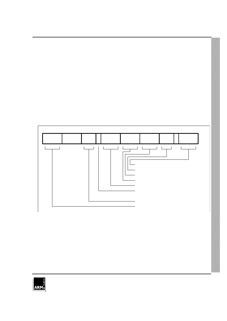
ARM Instruction Set - MRC, MCR
ARM7TDMI Data Sheet
ARM DDI 0029E
4-57
Open Access
4.16 Coprocessor Register Transfers (MRC, MCR)
The instruction is only executed if the condition is true. The various conditions are
defined in
➲
Table 4-2: Condition code summary on page 4-5. The instruction encoding
is shown in
➲
Figure 4-27: Coprocessor register transfer instructions.
This class of instruction is used to communicate information directly between
ARM7TDMI and a coprocessor. An example of a coprocessor to ARM7TDMI register
transfer (MRC) instruction would be a FIX of a floating point value held in a
coprocessor, where the floating point number is converted into a 32 bit integer within
the coprocessor, and the result is then transferred to ARM7TDMI register. A FLOAT of
a 32 bit value in ARM7TDMI register into a floating point value within the coprocessor
illustrates the use of ARM7TDMI register to coprocessor transfer (MCR).
An important use of this instruction is to communicate control information directly from
the coprocessor into the ARM7TDMI CPSR flags. As an example, the result of a
comparison of two floating point values within a coprocessor can be moved to the
CPSR to control the subsequent flow of execution.
Figure 4-27: Coprocessor register transfer instructions
4.16.1 The coprocessor fields
The CP# field is used, as for all coprocessor instructions, to specify which coprocessor
is being called upon.
The CP Opc, CRn, CP and CRm fields are used only by the coprocessor, and the
interpretation presented here is derived from convention only. Other interpretations
are allowed where the coprocessor functionality is incompatible with this one. The
conventional interpretation is that the CP Opc and CP fields specify the operation the
coprocessor is required to perform, CRn is the coprocessor register which is the
21
Cond
0
11
12
15
16
19
20
24
27
28
31
23
CP#
7
8
1110
CRn
CP
CRm
5
4
3
1
L
CP Opc
Rd
Coprocessor number
Coprocessor information
Coprocessor operand register
Coprocessor operation mode
Condition field
Load/Store bit
0 = Store to Co-Processor
1 = Load from Co-Processor
ARM source/destination register
Coprocessor source/destination register

ARM Instruction Set - MRC, MCR
ARM7TDMI Data Sheet
ARM DDI 0029E
4-58
Open Access
source or destination of the transferred information, and CRm is a second coprocessor
register which may be involved in some way which depends on the particular operation
specified.
4.16.2 Transfers to R15
When a coprocessor register transfer to ARM7TDMI has R15 as the destination, bits
31, 30, 29 and 28 of the transferred word are copied into the N, Z, C and V flags
respectively. The other bits of the transferred word are ignored, and the PC and other
CPSR bits are unaffected by the transfer.
4.16.3 Transfers from R15
A coprocessor register transfer from ARM7TDMI with R15 as the source register will
store the PC+12.
4.16.4 Instruction cycle times
MRC instructions take 1S + (b+1)I +1C incremental cycles to execute, where S, I and
C are as defined in
➲
6.2 Cycle Types on page 6-2.
MCR instructions take 1S + bI +1C incremental cycles to execute, where
b is the
number of cycles spent in the coprocessor busy-wait loop.
4.16.5 Assembler syntax
<MCR|MRC>{cond} p#,<expression1>,Rd,cn,cm{,<expression2>}
MRC
move from coprocessor to ARM7TDMI register (L=1)
MCR
move from ARM7TDMI register to coprocessor (L=0)
{cond}
two character condition mnemonic. See
➲
Table 4-2:
Condition code summary on page 4-5.
p#
the unique number of the required coprocessor
<expression1>
evaluated to a constant and placed in the CP Opc field
Rd
is an expression evaluating to a valid ARM7TDMI register
number
cn and cm
are expressions evaluating to the valid coprocessor register
numbers CRn and CRm respectively
<expression2>
where present is evaluated to a constant and placed in the
CP field

ARM Instruction Set - MRC, MCR
ARM7TDMI Data Sheet
ARM DDI 0029E
4-59
Open Access
4.16.6 Examples
MRC
p2,5,R3,c5,c6
; Request coproc 2 to perform operation 5
; on c5 and c6, and transfer the (single
; 32 bit word) result back to R3.
MCR
p6,0,R4,c5,c6
; Request coproc 6 to perform operation 0
; on R4 and place the result in c6.
MRCEQ p3,9,R3,c5,c6,2 ; Conditionally request coproc 3 to
; perform operation 9 (type 2) on c5 and
; c6, and transfer the result back to R3.

ARM Instruction Set - Undefined
ARM7TDMI Data Sheet
ARM DDI 0029E
4-60
Open Access
4.17 Undefined Instruction
The instruction is only executed if the condition is true. The various conditions are
defined in
➲
Table 4-2: Condition code summary on page 4-5. The instruction format
is shown in
➲
Figure 4-28: Undefined instruction.
Figure 4-28: Undefined instruction
If the condition is true, the undefined instruction trap will be taken.
Note that the undefined instruction mechanism involves offering this instruction to any
coprocessors which may be present, and all coprocessors must refuse to accept it by
driving CPA and CPB HIGH.
4.17.1 Instruction cycle times
This instruction takes 2S + 1I + 1N cycles, where S, N and I are as defined in
➲
6.2
Cycle Types on page 6-2.
4.17.2 Assembler syntax
The assembler has no mnemonics for generating this instruction. If it is adopted in the
future for some specified use, suitable mnemonics will be added to the assembler.
Until such time, this instruction must not be used.
Cond
0
24
27
28
31
5
4
3
1
011
xxxx
25
xxxxxxxxxxxxxxxxxxxx

ARM Instruction Set - Examples
ARM7TDMI Data Sheet
ARM DDI 0029E
4-61
Open Access
4.18 Instruction Set Examples
The following examples show ways in which the basic ARM7TDMI instructions can
combine to give efficient code. None of these methods saves a great deal of execution
time (although they may save some), mostly they just save code.
4.18.1 Using the conditional instructions
Using conditionals for logical OR
CMP
Rn,#p
; If Rn=p OR Rm=q THEN GOTO Label.
BEQ
Label
CMP
Rm,#q
BEQ
Label
This can be replaced by
CMP
Rn,#p
CMPNE Rm,#q
; If condition not satisfied try
; other test.
BEQ
Label
Absolute value
TEQ
Rn,#0
; Test sign
RSBMI Rn,Rn,#0
; and 2's complement if necessary.
Multiplication by 4, 5 or 6 (run time)
MOV
Rc,Ra,LSL#2
; Multiply by 4,
CMP
Rb,#5
; test value,
ADDCS Rc,Rc,Ra
; complete multiply by 5,
ADDHI Rc,Rc,Ra
; complete multiply by 6.
Combining discrete and range tests
TEQ
Rc,#127
; Discrete test,
CMPNE Rc,#” ”-1
; range test
MOVLS Rc,#”.”
; IF Rc<=” ” OR Rc=ASCII(127)
; THEN Rc:=”.”
Division and remainder
A number of divide routines for specific applications are provided in source form as
part of the ANSI C library provided with the ARM Cross Development Toolkit, available
from your supplier. A short general purpose divide routine follows.
; Enter with numbers in Ra and Rb.
;
MOV
Rcnt,#1
; Bit to control the division.
Div1
CMP
Rb,#0x80000000
; Move Rb until greater than Ra.
CMPCC Rb,Ra
MOVCC Rb,Rb,ASL#1
MOVCC Rcnt,Rcnt,ASL#1
BCC
Div1
MOV
Rc,#0

ARM Instruction Set - Examples
ARM7TDMI Data Sheet
ARM DDI 0029E
4-62
Open Access
Div2
CMP
Ra,Rb
; Test for possible subtraction.
SUBCS Ra,Ra,Rb
; Subtract if ok,
ADDCS Rc,Rc,Rcnt
; put relevant bit into result
MOVS
Rcnt,Rcnt,LSR#1
; shift control bit
MOVNE Rb,Rb,LSR#1
; halve unless finished.
BNE
Div2
;
; Divide result in Rc,
; remainder in Ra.
Overflow detection in the ARM7TDMI
1
Overflow in unsigned multiply with a 32 bit result
UMULL
Rd,Rt,Rm,Rn
;3 to 6 cycles
TEQ
Rt,#0
;+1 cycle and a register
BNE
overflow
2
Overflow in signed multiply with a 32 bit result
SMULL
Rd,Rt,Rm,Rn
;3 to 6 cycles
TEQ
Rt,Rd ASR#31
;+1 cycle and a register
BNE
overflow
3
Overflow in unsigned multiply accumulate with a 32 bit result
UMLAL
Rd,Rt,Rm,Rn
;4 to 7 cycles
TEQ
Rt,#0
;+1 cycle and a register
BNE
overflow
4
Overflow in signed multiply accumulate with a 32 bit result
SMLAL
Rd,Rt,Rm,Rn
;4 to 7 cycles
TEQ
Rt,Rd, ASR#31
;+1 cycle and a register
BNE
overflow
5
Overflow in unsigned multiply accumulate with a 64 bit result
UMULL
Rl,Rh,Rm,Rn
;3 to 6 cycles
ADDS
Rl,Rl,Ra1
;lower accumulate
ADC
Rh,Rh,Ra2
;upper accumulate
BCS
overflow
;1 cycle and 2 registers
6
Overflow in signed multiply accumulate with a 64 bit result
SMULL
Rl,Rh,Rm,Rn
;3 to 6 cycles
ADDS
Rl,Rl,Ra1
;lower accumulate
ADC
Rh,Rh,Ra2
;upper accumulate
BVS
overflow
;1 cycle and 2 registers
Note
Overflow checking is not applicable to unsigned and signed multiplies with a 64-bit
result, since overflow does not occur in such calculations.

ARM Instruction Set - Examples
ARM7TDMI Data Sheet
ARM DDI 0029E
4-63
Open Access
4.18.2 Pseudo-random binary sequence generator
It is often necessary to generate (pseudo-) random numbers and the most efficient
algorithms are based on shift generators with exclusive-OR feedback rather like a
cyclic redundancy check generator. Unfortunately the sequence of a 32 bit generator
needs more than one feedback tap to be maximal length (i.e. 2^32-1 cycles before
repetition), so this example uses a 33 bit register with taps at bits 33 and 20. The basic
algorithm is newbit:=bit 33 eor bit 20, shift left the 33 bit number and put in newbit at
the bottom; this operation is performed for all the newbits needed (i.e. 32 bits). The
entire operation can be done in 5 S cycles:
; Enter with seed in Ra (32 bits),
Rb (1 bit in Rb lsb), uses Rc.
;
TST
Rb,Rb,LSR#1
; Top bit into carry
MOVS
Rc,Ra,RRX
; 33 bit rotate right
ADC
Rb,Rb,Rb
; carry into lsb of Rb
EOR
Rc,Rc,Ra,LSL#12
; (involved!)
EOR
Ra,Rc,Rc,LSR#20
; (similarly involved!)
; new seed in Ra, Rb as before
4.18.3 Multiplication by constant using the barrel shifter
Multiplication by 2^n (1,2,4,8,16,32..)
MOV
Ra, Rb, LSL #n
Multiplication by 2^n+1 (3,5,9,17..)
ADDRa,Ra,Ra,LSL #n
Multiplication by 2^n-1 (3,7,15..)
RSB
Ra,Ra,Ra,LSL #n
Multiplication by 6
ADD
Ra,Ra,Ra,LSL #1; multiply by 3
MOV
Ra,Ra,LSL#1; and then by 2
Multiply by 10 and add in extra number
ADD
Ra,Ra,Ra,LSL#2; multiply by 5
ADD
Ra,Rc,Ra,LSL#1; multiply by 2 and add in next digit
General recursive method for Rb := Ra*C, C a constant:
1
If C even, say C = 2^n*D, D odd:
D=1:
MOV Rb,Ra,LSL #n
D<>1:
{Rb := Ra*D}
MOV
Rb,Rb,LSL #n
2
If C MOD 4 = 1, say C = 2^n*D+1, D odd, n>1:
D=1:
ADD Rb,Ra,Ra,LSL #n

ARM Instruction Set - Examples
ARM7TDMI Data Sheet
ARM DDI 0029E
4-64
Open Access
D<>1:
{Rb := Ra*D}
ADD
Rb,Ra,Rb,LSL #n
3
If C MOD 4 = 3, say C = 2^n*D-1, D odd, n>1:
D=1:
RSB Rb,Ra,Ra,LSL #n
D<>1:
{Rb := Ra*D}
RSB
Rb,Ra,Rb,LSL #n
This is not quite optimal, but close. An example of its non-optimality is multiply
by 45 which is done by:
RSB
Rb,Ra,Ra,LSL#2 ; multiply by 3
RSB
Rb,Ra,Rb,LSL#2 ; multiply by 4*3-1 = 11
ADD
Rb,Ra,Rb,LSL# 2; multiply by 4*11+1 = 45
rather than by:
ADD
Rb,Ra,Ra,LSL#3 ; multiply by 9
ADD
Rb,Rb,Rb,LSL#2 ; multiply by 5*9 = 45
4.18.4 Loading a word from an unknown alignment
; enter with address in Ra (32 bits)
; uses Rb, Rc; result in Rd.
; Note d must be less than c e.g. 0,1
;
BIC
Rb,Ra,#3
; get word aligned address
LDMIA Rb,{Rd,Rc}
; get 64 bits containing answer
AND
Rb,Ra,#3
; correction factor in bytes
MOVS
Rb,Rb,LSL#3
; ...now in bits and test if aligned
MOVNE Rd,Rd,LSR Rb
; produce bottom of result word
; (if not aligned)
RSBNE Rb,Rb,#32
; get other shift amount
ORRNE Rd,Rd,Rc,LSL Rb; combine two halves to get result
Wyszukiwarka
Podobne podstrony:
PANsound manual
als manual RZ5IUSXZX237ENPGWFIN Nieznany
hplj 5p 6p service manual vhnlwmi5rxab6ao6bivsrdhllvztpnnomgxi2ma vhnlwmi5rxab6ao6bivsrdhllvztpnnomg
BSAVA Manual of Rabbit Surgery Dentistry and Imaging
Okidata Okipage 14e Parts Manual
Bmw 01 94 Business Mid Radio Owners Manual
Manual Acer TravelMate 2430 US EN
manual mechanika 2 2 id 279133 Nieznany
4 Steyr Operation and Maintenance Manual 8th edition Feb 08
Oberheim Prommer Service Manual
cas test platform user manual
Kyocera FS 1010 Parts Manual
juki DDL 5550 DDL 8500 DDL 8700 manual
Forex Online Manual For Successful Trading
ManualHandlingStandingAssessment
Brother PT 2450 Parts Manual
Jabra CLIPPER Manual PL 10311 (1)
więcej podobnych podstron